Embed Size (px)
Citation preview

Quantum-Mechanical Modelingof Transport Parametersfor MOS Devices


Timm Hohr
Quantum-MechanicalModeling of Transport
Parameters for MOS Devices
Hartung-Gorre Verlag Konstanz2006

Reprint of Diss. ETH No. 16228
SERIES IN MICROELECTRONICS VOLUME 173
edited by Wolfgang FichtnerQiuting HuangHeinz JackelHans MelchiorGeorge S. MoschytzGerhard Troster
Bibliographic Information published by Die Deutsche Bibliothek
Die Deutsche Bibliothek lists this publication in the Deutsche Nationalbibliografie;detailed bibliographic data is available in the internet at http://dnb.ddb.de.
Copyright © 2006 by Timm Hohr
First edition 2006
HARTUNG-GORRE VERLAG KONSTANZ
ISSN 0936-5362
ISBN 3-86628-087-4

Acknowledgments
First of all, I would like to thank Prof. Wolfgang Fichtner for theopportunity to work and learn at the Institut fur Integrierte Systemewhere I found excellent working conditions as well as outstandingcolleagues. I am also grateful to Prof. Giorgio Baccarani for co-examining this thesis and his interest in my work.
Especially, I wish to thank Prof. Andreas Schenk for his reliablesupport and the valuable scientific advice he gave me during my timeat the Institute. I am indebted to Andreas Wettstein for providing abasis for my work regarding both theory and implementation of quan-tum modeling and for his support on both aspects. I thank MichaelPfeiffer and Bernhard Schmithusen for their help on compiling issues.Furthermore, I enjoyed the company and expertise of Frank Geelhaar,Frederik Heinz, Simon Brugger, Fabian Bufler, Christoph Muller, Ed-uardo Alonso and Beat Sahli.
In addition, I want to thank all the people who created the friendlyworking environment and kept everything working smoothly in thebackground. These are Dr. Dolf Aemmer and Dr. Norbert Felber, thesecretaries Christine Haller, Bruno Fischer, Margit Boksberger andVerena Roffler, and the technicians Hansjorg Gisler and HanspeterMathys. Last but not least, I would like to thank Christoph Wickiand Anja Bohm who provided and maintained the excellent computingenvironment.
I would like to acknowledge that parts of this work were financiallysupported by the Kommission fur Technologie und Innovation (KTI,Project 4082.2) and by Fujitsu.
v


Abstract
The ongoing evolution of integrated circuits is based on the minia-turization of the individual devices. Typical feature sizes that areroutinely implemented by today’s manufacturing technology alreadybelong to the domain of quantum effects. While this poses additionalproblems for traditional device concepts it also paves the road towardsnew functional principles. For assessing either aspects, appropriatemodels are needed for simulators, which have become an importanttool in both device and process engineering.
Topic of this thesis are the implications of quantization on trans-port parameters in drift-diffusion-based numerical descriptions of semi-conductor devices. For these investigations the device simulaton soft-ware DESSIS−ISE was used, especially its enhancements to modelquantum effects. These comprise a self-consistent Schrodinger-Poissonsolver for one-dimensional quantization effects and the quantum drift-diffusion (QDD) model.
In the first part of this work, the QDD model is applied to tun-neling through MOS gate oxides and double barrier devices. For bothstructures the “tunneling” characteristics exhibit regions of negativedifferential resistance which was identified as a modeling artifact.These results indicate that the QDD description of tunneling is ofonly very limited use.
The second part deals with the modeling of Shockley-Read-Hall(SRH) recombination – which is enabled by multiphonon processesbetween bands and deep trap levels in the gap of the semiconductor –in the presence of quantization. The corresponding density of stateswhich is used in the description of the carrier densities must alsobe applied to the SRH-lifetimes, i.e. these have to account for an
vii

viii ABSTRACT
additional energetic separation from the trap levels. This in turncauses a corresponding change in the SRH rate with respect to theusual semi-classical description.
The third part is devoted to modeling of the drift mobility inMOS channels. The main focus is put onto Coulomb scattering ationized impurities located in the substrate as well as in the polysili-con gate. The influence from the latter is commonly named “remotecharge scattering” (RCS) and suspected of contributing to the mo-bility degradation observed in thin-oxide devices. However, in thetreatment presented here, which includes screening by mobile chargein the gate, RCS was found not to have a great impact.

Zusammenfassung
Die fortdauernde Entwicklung von integrierten Schaltungen basiertauf der stetigen Miniaturisierung des einzelnen Bauelements. Die mitheutigen Herstellungsverfahren routinemassig realisierten Struktur-grossen gehoren bereits zum Einflussbereich quantenmechanischer Ef-fekte. Dies bedeutet zum einen weitere Probleme fur die Konzeptionherkommlicher Schaltungsbausteine, auf der anderen Seite eroffnet esaber auch Wege zu neuen Funktionsprinzipien. Zur Bewertung bei-der Aspekte werden Modelle fur den Einsatz in Simulatoren benotigt,welche ein wichtiges Werkzeug fur sowohl Bauelement- als auch Pro-zessentwicklung geworden sind.
Thema dieser Arbeit sind die Auswirkungen der Quantisierung aufTransportparameter in einer Drift-Diffusions-basierten, numerischenNachbildung von Halbleiterbauelementen. Zu diesem Zweck wurdeder Bauelementsimulator DESSIS−ISE verwendet, insbesondere dieErweiterungen zur Modellierung von Quanteneffekten, die ein selbst-konsistentes Verfahren zur Losung der Schrodinger- und der Poisson-Gleichung fur Quantisierung in einer Dimension und ein Quanten-Drift-Diffusions (QDD) Modell umfassen.
Im ersten Teil dieser Arbeit wird das QDD-Modell zur Beschrei-bung des Tunnelns durch MOS Gate-Oxide und Doppelbarrieren ein-gesetzt. Fur beide Strukturen weisen die Tunnelkennlinien Abschnit-te mit einem negativen differentiellen Widerstand auf, der als Arte-fakt des Modells identifiziert wurde. Diese Ergebnisse zeigen, dass dieQDD-Beschreibung des Tunnelns nur von sehr begrenztem Nutzen ist.
Der zweite Teil beschaftigt sich mit der Modellierung der Shockley-Read-Hall (SRH) Rekombination – welche durch Multiphononenpro-zesse zwischen den Bandern und tiefen Haftstellen in der Bandlucke
ix
x ZUSAMMENFASSUNG
des Halbleiters zustandekommt – in der Gegenwart von Quantisierung.Falls die entsprechende Zustandsdichte in konsistenter Weise sowohlzur Beschreibung der Ladungstragerdichten als auch der SRH-Lebens-dauern verwendet wird, so mussen letztere ebenso einen zusatzlichenenergetischen Abstand zu den Haftstellenniveaus widerspiegeln. Die-ses wiederum bedingt eine entsprechende Anderung der SRH-Rategegenuber der ublichen semiklassischen Beschreibung.
Der dritte Teil ist der Modellierung der Driftbeweglichkeit in MOS-Kanalen gewidmet. Das Hauptaugenmerk liegt auf der Coulombstreu-ung an ionisierten Storstellen, die sich sowohl im Substrat als auchim Polysilizium-Gate befinden. Der Einfluss letzterer wird allgemeinals “remote charge scattering” (RCS) bezeichnet und es wird ver-mutet, dass er zu einer Beweglichkeitsverschlechterung beitragt, diein Bauelementen mit dunnen Oxiden beobachtet wird. In der hiervorgestellten Betrachtung, die die Abschirmung durch bewegliche La-dungstrager im Gate einschliesst, wurde jedoch festgestellt, dass RCSkeinen grossen Einfluss hat.

Contents
Acknowledgments v
Abstract vii
Zusammenfassung ix
1 Introduction 1
2 Quantization Models 52.1 The one-electron Schrodinger equation in the effective
mass approximation . . . . . . . . . . . . . . . . . . . 52.2 The Density Gradient Model . . . . . . . . . . . . . . 10
2.2.1 The quantum drift-diffusion model for constanteffective mass . . . . . . . . . . . . . . . . . . . 11
2.2.2 Generalizations . . . . . . . . . . . . . . . . . . 16
3 Density-Gradient Modeling of Tunneling through In-sulators 193.1 Barrier tunneling with QDD and the Schrodinger-Bardeen
method . . . . . . . . . . . . . . . . . . . . . . . . . . 203.2 Simulated devices and results . . . . . . . . . . . . . . 22
3.2.1 N-channel MOSFET . . . . . . . . . . . . . . . 223.2.2 MOS-diode . . . . . . . . . . . . . . . . . . . . 243.2.3 Resonant tunneling diode . . . . . . . . . . . . 283.2.4 N-MOSFET off-state leakage . . . . . . . . . . 29
3.3 Conclusions . . . . . . . . . . . . . . . . . . . . . . . . 31
xi

xii CONTENTS
4 Revised Shockley-Read-Hall Lifetimes for Quantum Trans-port Modeling 354.1 Model for the SRH lifetime . . . . . . . . . . . . . . . 36
4.1.1 Rate formula . . . . . . . . . . . . . . . . . . . 364.1.2 Capture rate for multiphonon transitions . . . 404.1.3 Density of states for quantization in one dimension 414.1.4 Electron lifetime profiles . . . . . . . . . . . . . 43
4.2 Lifetime profiles for a triangular well . . . . . . . . . . 454.3 Analytical approximation for strong quantum confine-
ment . . . . . . . . . . . . . . . . . . . . . . . . . . . . 504.4 Lifetime profiles for simulated devices . . . . . . . . . 54
4.4.1 Metal-oxide-semiconductor diode . . . . . . . . 544.4.2 Quantum-well diode . . . . . . . . . . . . . . . 56
4.5 Conclusions . . . . . . . . . . . . . . . . . . . . . . . . 60
5 Quantum-Mechanical Modeling of the Low-Field DriftMobility in MOS Devices 635.1 Effective mobility extraction . . . . . . . . . . . . . . . 645.2 Relaxation time approximation . . . . . . . . . . . . . 66
5.2.1 Drift mobility . . . . . . . . . . . . . . . . . . . 685.3 Coulomb scattering . . . . . . . . . . . . . . . . . . . . 70
5.3.1 Screening . . . . . . . . . . . . . . . . . . . . . 705.3.2 Fluctuations of the impurity density . . . . . . 76
5.4 Interface roughness . . . . . . . . . . . . . . . . . . . . 805.5 Phonons . . . . . . . . . . . . . . . . . . . . . . . . . . 865.6 Results . . . . . . . . . . . . . . . . . . . . . . . . . . . 87
5.6.1 Effective field . . . . . . . . . . . . . . . . . . . 875.6.2 Depth of the gate quantum region . . . . . . . 875.6.3 Screened Coulomb potential . . . . . . . . . . . 895.6.4 Coulomb-scattering-limited mobility . . . . . . 925.6.5 Total effective mobility . . . . . . . . . . . . . 975.6.6 Test of simplifications . . . . . . . . . . . . . . 1005.6.7 Comparison to literature data . . . . . . . . . . 102
5.7 Discussion . . . . . . . . . . . . . . . . . . . . . . . . . 106A Local density of states . . . . . . . . . . . . . . . . . . 111
A.1 Bulk case with almost constant potential . . . 111A.2 Local DOS in an electric field . . . . . . . . . . 112A.3 Local DOS for bound states . . . . . . . . . . . 113

CONTENTS xiii
B Green’s function . . . . . . . . . . . . . . . . . . . . . 115C Polarization factor . . . . . . . . . . . . . . . . . . . . 119
Bibliography 123
Curriculum Vitae 133


Chapter 1
Introduction
As Moore’s law continues to prevail since the 1960’s it has attained thestatus of a self-fulfilling prophecy. The statement that the number ofcomponents on a chip doubles every 18 months1 has become the basisfor the formulation of milestones along the international technologyroadmap for semiconductors (ITRS) [2]. The breakdown of this expo-nential development has been predicted several times in the past butup to now all obstacles (so-called “red bricks”: problems for whichno manufacturable solutions are known) have been either removed orcircumvented by investing an ever growing amount of resources.
Sustaining the current rate of miniaturization requires simultane-ous efforts in several fields. At the device level design parameters,such as geometry and doping profiles, have to be engineered as wellas materials and process steps. In this context, numerical device sim-ulations enable the optimization of device designs without having toexplore all possible variations by cost- and time-consuming prototyp-ing. Furthermore, device simulations allow the exploration of futuredevice types that can not yet be produced with available technolo-gies. In order to fulfill these tasks accurate models are needed for thephysical mechanisms that govern the device behavior.
At the heart of these efforts lies the shrinkage of the smallest op-
1Actually, there are a lot of different formulations being named as “Moore’slaw”. Originally, Moore predicted an increase by a factor of two per year for thedecade between 1965 and 1975 [1].
1

2 CHAPTER 1. INTRODUCTION
erating component of a chip which in most cases is the metal-oxide-semiconductor field effect transistor (MOSFET), which has been theworkhorse of semiconductor industry for several decades. As its di-mensions continue to shrink, conventional short channel effects, whichhave been of major concern for quite some time, become even moresevere. Examples for these effects are decreasing threshold voltagesfor short devices and drain induced barrier lowering (DIBL). Theseeffects can cause considerable off-state leakage currents. A newer issueis the growing importance of statistical variations in the microscopiccomposition of the devices. For example, the variation of the numberof dopants within the shrinking active device area causes unwanted“random dopant fluctuations” of the characteristics. Another issueis quasi-ballistic transport: Electrons that cross a smaller device mayexperience fewer scattering events and higher fields. The Monte Carlomethod is an established tool for simulating these effects.
In order to maintain control over the shorter channel the scalinglaws for MOSFETs require a proportional decrease of the gate oxide.This reduction introduces tunneling currents, which is another sourceof leakage and therefore of great concern. If a polysilicon gate is used(which is common practice because it allows a self-aligned creation ofthe source and drain regions) the intended gain in capacitance may behampered by gate depletion. In addition, a degradation of the effec-tive mobility has been observed for thin-oxide MOSFETs. A possibleexplanation might be an enhanced scattering of channel carriers dueto the proximity of ionized impurities in the gate (“remote chargescattering”, RCS).
In addition, conventional transistor scaling has already reached aregime where quantum effects are of importance. Oxide thicknessesand inversion layer depths are reaching values below the thermal de-Broglie wavelength of the electron. Thus, the inclusion of quantumeffects has become crucial for the modeling of modern deep-submicrondevices. Corresponding enhancements of conventional drift-diffusiondevice simulators are widely used by applying Schrodinger solvers ordensity gradient models. These methods provide good results for thequantum-mechanical (QM) carrier density profiles. For example, theinclusion of QM densities enables the modeling of quantum depletioneffects, i.e. the decrease of the carrier density towards a potentialbarrier which is a consequence of the shape of the wave functions.

3
In MOSFETs this effect causes a shift in the threshold voltage withrespect to classical modeling. An introduction to the quantizationmodels in the device simulator DESSIS−ISE , on which this work isbased, is given in chapter 2.
Quantization does not only shape the density distribution but alsoaffects carrier transport. This work deals with some aspects of devicemodeling that contain both quantum effects and transport phenom-ena. Most pure in this regard is tunneling as it lacks a classical coun-terpart. Next to the unwanted leakage currents through the gate insu-lator and the source-to-drain barrier in conventional CMOS devices,tunneling plays a key role for novel device concepts such as singleelectron transistors, quantum dot devices or tunneling transistors.
Modeling of oxide tunneling in MOS structures has been exploredover a long time [3–5]. Common models apply transmission coeffi-cients, transfer Hamiltonians, transfer matrix methods or lifetimesof quasi-bound states. All these methods make use of the quantummechanical states of the MOS system by applying either plane-wave,analytical or numerically exact solutions, or use the Wentzel-Kramers-Brillouin (WKB) approximation. It is interesting to see whether den-sity gradient models, which do not resort to the QM wave functionsand eigenenergies, can also be applied to this problem as they havealready proven their capabilities in the modeling of quantum deple-tion effects. In chapter 3 this is tested for the quantum drift-diffusionmodel of the DESSIS−ISE device simulator.
Next to tunneling, there are other aspects of transport modelingwhich already exist in classical device simulations. These are thetransport parameters in the drift-diffusion model: The drift mobility,which is the most important one, and the generation-recombinationlifetimes. Having models for the quantum mechanical carrier densitiesat hand, the question arises how these other quantities can be modeledin a consistent way.
In contrast to Monte Carlo simulations where single scatteringevents and their influence on the carrier trajectories are modeled, thedrift-diffusion description summarizes all these processes into a singleparameter, the drift mobility. In modeling the inversion layer mo-bility it is essential to incorporate the carrier wave functions whichare needed for the calculation of the scattering matrix elements. Inthis regard QM effects have been considered for a long time, beginning

4 CHAPTER 1. INTRODUCTION
with Stern and Howard in 1967 [6], although limited to the lowest sub-band (“electric quantum limit”) and a variational analytic expressionfor the wave function square. As mentioned above, RCS may cause areduction of the mobility for thin gate oxides. In order to analyze theimportance of this effect calculations of the effective mobility in MOSstructures have been performed which included electron-phonon, in-terface roughness and Coulomb scattering (chapter 5). For the latter,screening effects by the QM eigenstates of the mobile carriers are ofcrucial importance.
The implications of quantum confinement on Shockley-Read-Hallrecombination (SRH, non-radiative recombination via deep trap lev-els) have not received much attention in the literature, yet. It isknown, however, that tunneling in combination with multiphononprocesses leads to enhanced recombination rates in high electric fieldswhich can be modeled by reduced lifetimes. Based on that, chapter 4investigates possible impacts of quantization on SRH recombination.

Chapter 2
Quantization Models
2.1 The one-electron Schrodinger equationin the effective mass approximation
A very important concept which underlies all subsequent considera-tions in this text is the effective mass approximation (EMA). In prin-ciple, the potential in a semiconductor or any other crystal stronglyvaries within and with the periodicity of the inter-atomic distance.However, any potentials that arise from externally applied fields or areintroduced by doping gradients (or, generally, impurities, i.e. pertur-bations of the perfect lattice) often vary on a much longer length scale.The periodic potential inherent to the crystal can then be viewed asa, albeit strong, modulation of these external potentials.
The purpose of the EMA is, in short, to get rid of this periodic partof the potential and to obtain an equation of the Schrodinger type forwave functions that are only subject to the long range part of the po-tential. Simultaneously, however, the impact of the periodic potentialis not removed completely but is lumped into the effective mass thatreplaces the electron mass in the kinetic part of the Hamiltonian.
The starting point for the EMA itself is a one-electron Schrodingerequation, which already involves the assumption of fixed ionic coreson the sites of a Bravais lattice and the Hartree approximation of thein principle many-body interaction between a vast number of elec-
5

6 CHAPTER 2. QUANTIZATION MODELS
trons. Exchange correlation effects are neglected as well. In the pres-ence of an external potential U the one-electron Schrodinger equationreads [7] (
H0 + U(r))Ψi(r) = EiΨi(r) , (2.1)
where H0 is the crystal Hamiltonian, which contains the kinetic part,the electron-core interaction and the Hartree potential. The wavefunction Ψ can be expanded into eigenvectors φkα(r) of H0:
Ψi(r) =∑kα
Fαi (k)φkα(r) =
∑kα
Fαi (k)
eikr
√Ω
uαk(r) , (2.2)
where φkα(r) and uαk(r) are the Bloch function and factor for the αthband, respectively, and Ω is a normalization volume.
It is then assumed that U(r) varies slowly which means that ev-erywhere within the Wigner-Seitz cell that contains the vector r thepotential U can be approximated by its value at the center R of thatcell: U(r) ≈ U(R). The expansion coefficients Fα
i (k) are then foundto be the Fourier coefficients of an envelope wave function Fα
i (r) whichsolves the Wannier equation [7–9]:
(Eα(−i∇) + U(r))Fαi (r) = EiF
αi (r) , (2.3)
where Eα(k) denotes the electronic band structure, i. e. the dispersionrelation between single-electron eigenvalues and wave vectors in theαth band. Furthermore, it is assumed that the envelope functionis sufficiently smooth so that Fα
i (k) in (2.2) has a strong peak atk = 0 and that a solution for the eigenvalue Ei exists only within oneband, labeled α in the following. Then the full wave function can beapproximated as
Ψi(r) ≈ 1√Ω
F αi (r)uα0(r) . (2.4)
Also, for a smooth envelope function the band structure can be ex-panded to quadratic order around its extremum k0 to yield an equa-tion of the Schrodinger type (parabolic approximation):(
− 2
2∇ · (m−1
k0
)∇ + U(r) + Eα(k0)︸ ︷︷ ︸=:Eα
c,v(r)
)F αi (r) = EiF
αi (r) , (2.5)

2.1. THE SCHRODINGER EQUATION 7
where mk0 is the effective mass tensor at k0. The extremum of theband structure together with the external potential gives the bandedge Eα
c,v(r); the indices c and v denote conduction and valence band,respectively.
Although the above derivation assumes a bulk crystal it is oftenalso applied in the presence of interfaces between materials with differ-ent band structures. Therefore, band edge steps ΦB(r) are introducedvia a spatial dependency in E(k0). But also the effective mass and thelocation k0 of the valleys in the Brillouin zone become functions ofposition r. In the following the spatially varying band edge potentialis denoted by Φ = U +ΦB .
For a position-dependent mass it is not initially clear that thechosen form (cf. (2.5) which is suggested in Ref. [10]) of the kineticpart is correct [11]. The discussion in Ref. [12] for a one-dimensionalproblem, however, supports it.
Decoupling into 1D and 2D parts
In semiconductor devices one often encounters a situation where thepotential Φ varies relatively strongly along one dimension, say alongthe z-coordinate, but rather weakly along the two others. It maythen suffice to solve the one-dimensional Schrodinger equation alongthe z-direction, i. e. to make a separation ansatz for the envelopeFi(r) = ψn(z)χκ(x, y) and approximate the functions χκ as a contin-uum of plane waves.1 Along the z-direction, however, the carriers areconfined into discrete levels and may not move freely. This approachdescribes a two-dimensional electron gas (2DEG).2 The channel of aMOSFET is the typical example of a semiconductor region where sucha description applies.
The decoupling not only depends on the form of the potential partbut also on the kinetic part, i.e. the band structure. The separation isnot possible in a coordinate system in which the inverse effective masstensor has non-zero off-diagonal elements that couple the derivativeswith respect to the z- and x, y-coordinates. Including non-parabolicityposes a similar problem [11]. Therefore, it is assumed in the following
1This is only possible if the potential Φ is a sum of the form Φ(x, y, z) =v(z) + w(x, y) + u(x, y, z) and if the coupling term u is small [11].
2For other dimensionalities of the electron gas see for example Ref. [13].

8 CHAPTER 2. QUANTIZATION MODELS
that the coordinate system coincides with the principal axes of m−1k0
:(−
2
2∂
∂z
1mz(z)
∂
∂z+Φ(z)
)ψn(z) = Enψn(z) (2.6)
The chosen form of the kinetic part implies the continuity of ψn
and m−1(z)dψn/dz across the interface [10].
Density
For multi-valley semiconductors like silicon, several Schrodinger equa-tions must be solved, one for each valley with its center position k0
requiring in general an individual mass tensor m−1(k0). In the fol-lowing we will refer to silicon, where the the six valleys divide intotwo equivalent sets for the chosen coordinate system.
Once the eigenenergies and eigenfunctions have been found thedensity profile n(z) can be computed as the sum over the probabilitydensity of all states weighted with the distribution function f . Thesummation occurs over the valley index ν, the quantum number n ofthe eigenvalues, the quantum numbers of the in-plane motion (givenby the components of the in-plane wave vector κ), and the spin σ:
n(z) =∑
nν,κ,σ
|ψnν(z)|2∣∣∣∣∣ eiκx‖√
LxLy
∣∣∣∣∣2
f(Enν + Eνκ) (2.7)
=∑nν
|ψnν(z)|2∫
dEZν2D(E)f(Enν + E) . (2.8)
The summation over the spin index is absorbed as a factor of two inthe two-dimensional density of states:
Zν2D(E) =
mνxy
π2(1 + 2αE) , where mν
xy =√
mνxm
νy . (2.9)
The factor α = 0.5 (eV)−1 accounts for non-parabolicity in the in-plane part of the band structure of silicon [14]. The following consid-erations, however, are restricted to parabolic bands, i.e. α = 0.
If there is no current flow along the z-direction the function f isthe Fermi distribution:
f0(E) =1
1 + exp(E−EFkT
) . (2.10)
2.1. THE SCHRODINGER EQUATION 9
Then the density profile is (using α = 0):
n(z) =kT
π2
∑ν
mνxy
∑n
|ψnν(z)|2 F0
(EF − Enν
kT
), (2.11)
with the Fermi integral of zeroth order:
F0(x) = ln(1 + exp(x)
). (2.12)
In practice, eigensolutions for the Schrodinger equation are only com-puted up to a certain maximum energy. If this limit is too low (e. g.in order to speed up the computation) to resemble the full density toa reasonable degree then a classical correction should be added [11].
1D Schrodinger solver
The numerical results in this work were calculated using the 1D Schro-dinger-Poisson solver that was integrated into the device simulationsoftware DESSIS−ISE by Wettstein [11, 15]. The following short de-scription is based on the above references where further details can befound.
The Schrodinger equation (2.6) is solved on extracted one-dimen-sional finite domains of the simulated device. The boundary condi-tions are suited for bound solutions and reflect the exponential decayinto a barrier that is assumed to continue towards infinity at a con-stant height Φ(zB):
∂ψnν(zB)∂z
/ψnν(zB) = ±
√2mν
z (Enν − Φ(zB))2
. (2.13)
The sign must be chosen for each end zB of the domain to appropri-ately describe a decay into the outside region.
The solver is based on a shooting method: A value for Env isguessed which transforms the eigenvalue problem into an initial valueproblem that is solved by propagating the wave function from bothends of the domain towards the inside. If both parts match at amiddle point then Enν is an eigenvalue. Otherwise it is adjustediteratively [11].

10 CHAPTER 2. QUANTIZATION MODELS
Self-consistency is achieved by placing the solver inside the itera-tion for the Poisson equation. In contrast to the classical situation, theproblem arises that the density depends non-locally on the potential.Thus the Jacobian, i. e. the derivatives of the density with respect tothe potential, can not be obtained using a simple local relation amongthem, neither is it sparse anymore.
2.2 The Density Gradient Model
The density gradient (DG) model provides a description of transportin terms of macroscopic quantities, e.g. densities of the particles andtheir currents. In this respect, it is similar to the classical hydrody-namic transport and drift-diffusion model but in addition it includescontributions that account for certain aspects of the quantum natureof the particles. This is done without explicit knowledge of micro-scopic information like eigenenergies and wave functions.
All above-mentioned models have in common that they can bederived by applying the method of moments [16–18] to an underly-ing microscopic transport equation. In the classical case this is theBoltzmann transport equation.
Soon after the presentation of quantization as an eigenvalue prob-lem [19] in 1926, Madelung showed that Schrodinger’s new equationcould be cast into a hydrodynamic form [20]. The form of the quan-tum correction seen later in this chapter already appeared at this earlystage of wave mechanics.
First developments of the DG model by Ancona et al. took theopposite direction, starting from a macroscopic description [21]. Theyuse thermodynamic considerations introducing a lowest order depen-dency on the density gradient into the internal energy per particle andreach an equation of the Schrodinger type for a static one-dimensionalsystem. Thereby the prefactor of the gradient term can be identifiedand linked to Planck’s constant.
Following derivations were based on or linked to quantum statisti-cal mechanics, i.e. the microscopic transport is described by either theWigner-Boltzmann equation [22] or its Fourier transformed counter-part, the Quantum-Liouville or von-Neumann equation which governsthe evolution of the density matrix [23]. Applying the method of mo-

2.2. THE DENSITY GRADIENT MODEL 11
ments yields the classical transport models with additional quantumcorrections which are then called quantum hydrodynamic (QHD) [24]and quantum drift-diffusion (QDD) model. To close the moment hi-erarchy an approximation for the density matrix is needed which canbe obtained as a perturbation with respect to the free-particle so-lution [25]. Wettstein uses a similar approach but also includes aspatially varying effective mass [11].
In the next section we will trace the derivation of the quantumdrift-diffusion model which is implemented in the simulation toolDESSIS−ISE that was used for this thesis [26, 27].
2.2.1 The quantum drift-diffusion model for con-stant effective mass
This section closely follows the derivation given in Ref. [11]. However,it is assumed here that the effective mass does not depend on position.Starting point is the collision-free quantum Liouville equation(
i∂t − 2(m−1)ij ∂Ri
∂rj+ Φ(R+ r/2)− Φ(R− r/2)
)ρ(R, r) = 0
(2.14)for the density matrix of the statistical operator ρ in the center ofmass representation
ρ(R, r) = 〈R− r/2| ρ |R+ r/2〉 . (2.15)
In (2.14) and in the following the Einstein convention is used, i.e.summation over repeated indices is implied.
The kth moment of this equation is obtained by differentiating ktimes with respect to the distance coordinate r and taking the limit ofvanishing r. Corresponding moments of the density matrix are definedand identified with variables in the resulting moment equation whichonly depend on R (and time t). The first two moments (k = 0, 1) arethe particle density n and the current density j:
n(R) = limr→0
ρ(R, r) (2.16)
js(R) = i (m−1)su limr→0
∂ruρ(R, r) , for s = 1, 2, 3 . (2.17)

12 CHAPTER 2. QUANTIZATION MODELS
The zeroth moment of (2.14) is immediately obtained as the continuityequation for the density:
∂tn + ∇ · j = 0 . (2.18)
The first moment is the continuity equation for the current density:
mlk∂tjk − 2(m−1)su ∂Rs
limr→0
∂ru∂rl
ρ + n∂RlΦ = 0 . (2.19)
Collisions are introduced by adding a net generation-recombinationrate G and a momentum relaxation time τm on the right hand side ofEqs. (2.18) and (2.19) which then read
∂tn + ∇ · j = G (2.20)
andmlk∂tjk −
2(m−1)su ∂Rslimr→0
∂ru∂rl
ρ + n∂RlΦ
= mlkjk
(G
n− 1
τm
).
(2.21)
By closing the hierarchy of equations at this stage a density gradientcorrection to the drift-diffusion equations (also called quantum drift-diffusion, QDD) is obtained. This closure requires an expression forthe term containing limr→0 ∂ru∂rlρ, which is a second order moment.
Assuming that the situation is not too far from equilibrium one canuse the equilibrium density matrix ρeq for this purpose. In the caseof a vanishing potential Φ ≡ 0 the corresponding density matrix ρ0
eq isknown because the solutions of the free-particle Hamiltonian H0 areavailable as plane waves. For non-vanishing potential Φ, however, theeigensolutions for the corresponding operator ρeq = exp(−β(H0 +Φ))are not known because the aim of the whole method is to avoid solvingthe Schrodinger equation.
Therefore, the potential Φ is treated as a perturbation of the free-particle Hamiltonian H0. This perturbation is included to first orderusing the approximation [11]
ρeq ≈ ρ0eq −
∫ β
0
dβ′e−(β−β′)H0Φe−β′H0 . (2.22)

2.2. THE DENSITY GRADIENT MODEL 13
The corresponding approximate equilibrium density matrix is
ρeq(R, r) = 〈R− r/2| ρeq |R+ r/2〉
≈ ρ0eq(r)−
∫ β
0
dβ′∫
d3x ρ0
(β−β′,R− r
2−x
)Φ(x) ρ0
(β′,x−R− r
2
),
(2.23)
with the free-particle density matrix
ρ0eq(R, r) =
√detm
(2π2β)3exp
(−rTmr
2β2
)=: ρ0(β, r) , (2.24)
which also provides the definition of the auxiliary expression ρ0(β, r).The matrix m denotes the effective mass tensor and β = 1/kT theinverse temperature.
By substituting x = R+R′ and β′ = β(1 + λ)/2 the second termin (2.23) becomes
−β
2
∫ 1
−1
dλ
∫d3R′
√detm
(π2β(1−λ))3exp
(−(R′ + r
2 )Tm (R′ + r
2 )β(1− λ)2
)
×Φ(R+R′)
√detm
(π2β(1+λ))3exp
(−(R′ − r
2 )Tm (R′ − r
2 )β(1 + λ)2
).
(2.25)
By rearranging the exponents and substituting λ → −λ it can be castinto the form
ρ0eq β V (R, r) , (2.26)
where a factor ρ0eq was extracted leaving a potential V defined as
V (R, r) =12
∫ 1
−1
dλ
∫d3R′
√23 detm
(π2β(1−λ2))3
× exp(−(2R′ − λr)Tm (2R′ − λr)
2β(1− λ2)2
)Φ(R+R′) .
(2.27)
It is further assumed that |β V | 1, so that the total density matrixρeq = ρ0
eq(1− βV ) can be approximated by ρeq ≈ ρ0eq exp(−βV ).3
3The term −βV equals Wettstein’s log ρqm [11].

14 CHAPTER 2. QUANTIZATION MODELS
With this factorization ansatz for ρ, the second order moment inthe current equation (2.21) can be further decomposed yielding thediffusion term, a term quadratic in j and the quantum correctioncontaining V :
− 2(m−1)su ∂Rs
limr→0
∂ru∂rl
ρ = ∂Rl
(n
β
)+ mlu∂Ri
(jijun
)+
2(m−1)ij ∂Ri
(n lim
r→0∂rj∂rlβV
). (2.28)
With the use of the continuity equation (2.20) and some rearrange-ments the current equation (2.21) becomes
∂Rl
(n
β
)+
2(m−1)ij ∂Ri
(n lim
r→0∂rj
∂rlβV
)+ n∂RlΦ+ (n∂t + ji∂Ri)
(mlkjk
n
)= −mlkjk
τm. (2.29)
What is left is to calculate limr→0
∂rj∂rl
βV . Using (2.27) one obtains
limr→0
∂rj∂rl
βV =β
2
∫ 1
−1
dλλ2
4∂Rj
∂Rlv(λ,R) , (2.30)
where v is the potential Φ convoluted with a Gaussian smoothingfunction:
v(λ,R) =
√23 detm
(π2β(1−λ2))3
∫d3R′ exp
(− 2R′TmR′
β(1−λ2)2
)Φ(R+R′)
(2.31)
=∫
d3ξ
π3/2e−|ξ|2Φ(R+ lqm ξ) , (2.32)
with lqm =√
β(1−λ2)2/2m. In the second line an isotropic effectivemass m is assumed.4 For λ = 0 the maximum width of the Gaussian,lqm, is the thermal de-Broglie wavelength divided by 2
√π.
4This is only applied to obtain a simpler form of the second order term in thesubsequent Taylor expansion.

2.2. THE DENSITY GRADIENT MODEL 15
Now it is assumed that the potential Φ varies only slowly on thelength scale of smoothing, so that a Taylor expansion around R canbe used. Terms of odd orders in ξ vanish leaving
v(λ,R) ≈ Φ(R) +β(1−λ2)2
8m∆Φ(R) +O(4) . (2.33)
Thus, the quantum correction is given by
limr→0
∂rj∂rl
βV = ∂Rj∂Rl
(β
12Φ +
β2
2
240m∆Φ + . . .
). (2.34)
Retaining only the lowest order and dropping terms quadratic in j,equation (2.29) becomes
∂Rl
(n
β
)+
2
12(m−1)ij ∂Ri
(n∂Rj
∂RlβΦ
)+ n∂Rl
Φ
+ n∂t
(mlkjk
n
)= −mlkjk
τm. (2.35)
The quantum correction is now expressed by derivatives of knownquantities instead of more complicated integrals. The following sectionis devoted to its final form.
Although being only the zeroth order moment of ρ the density ncan be expanded in the same manner as the second order moment:
n =(limr→0
ρ0eq
)exp
(−β
2
∫ 1
−1
dλ v(λ,R))
(2.36)
≈(
m
2π2β
)3/2
exp(−β
(Φ +
β2
12m∆Φ +O(4)
)). (2.37)
If only the lowest order in Φ is retained, an approximate relation isfound between the density and the potential:
logn ≈ −βΦ + const. (2.38)
This can be used to express the quantum term by a “quantum poten-tial” Λ (for isotropic mass m and constant temperature):
2
12m∂i(n∂l∂iβΦ) =
2β
12mn ((∂i logn)∂l∂iΦ + ∂l∆Φ) ≈ n∂lΛ (2.39)

16 CHAPTER 2. QUANTIZATION MODELS
with two equivalent definitions for Λ that use either the potential orthe density:5
Λ =γ
2β
12m
(∆Φ− β
2(∇Φ)2
)(2.40)
= − γ2
12m
(∆ logn +
(∇ logn)2
2
)= −γ
2
6m∆√
n√n
, (2.41)
where a fit factor γ is added to compensate for the assumption of anisotropic effective mass m which is chosen to be the density of statesmass [11].
Alternatively, one could argue that in thermodynamic equilibriumEq. (2.35) yields
∂l logn ≈ −β∂l
(Φ+
2β
12m
(∆Φ− β
2(∇Φ)2
))+O(4) , (2.42)
which leads to (2.38–2.41) as well.Although inconsistent because the inclusion ofO(2)-terms in logn
has been neglected in the first place, one can plug (2.40) into (2.42)and this, in turn, into (2.41) to motivate the following equation for Λ:
Λ =γ
2β
12m
(∆(Φ + Λ)− β
2(∇Φ + ∇Λ)2
). (2.43)
Wettstein obtained this formula by arguing that the deliberate addi-tion of Λ on the right hand side of (2.40) introduces only an error ofthe order of
4. An equivalent equation was also presented in [28].In the stationary case Eq. (2.35) finally reads
kTµ∇n + µn∇(Φ + Λ) = −ej , (2.44)
where the mobility µ = eτm/m was introduced.
2.2.2 Generalizations
So far, only the spatial variations in the band edge potential Φ = V +ΦB have been taken into account. Wettstein’s more general derivation
5The second formulation gives the reason for the name “density gradientmodel”.

2.2. THE DENSITY GRADIENT MODEL 17
has also included a spatially varying effective mass [11]. This leadsto an additional term Φm = −3
2kT log(m/m0) that is introduced viareplacing Φ by Φ + Φm in Eqs. (2.43) and (2.44). The factor m0 isan arbitrary normalization constant.
In thermodynamic equilibrium the Fermi level EF can be addedin the expression for the density:6
n = Nc exp(β(EF − Φ)
), (2.45)
where Nc is the effective density of states of the conduction band andΦ = Φ+Φm+Λ is an “effective band edge” modified by the quantumpotential and the mass contribution. For vanishing Λ and Φm theusual classical expression is obtained.
In order to describe non-equilibrium, however, the model has beenextended by introducing additional parameters ξ and η into the dif-ferential equation for the quantum correction [27]:
Λ =γ
2β
12m
(∆Φξ,η − β
2
(∇Φξ,η
)2)
, (2.46)
with Φξ,η := Φ + (η − 1)Φ− ξEF = ηΦ + ΦB + Λ+ Φm − ξEF.Setting ξ = η = 1 corresponds to inserting (2.45) into (2.41), i.e.
the Fermi level enters through the choice of a specific model for thedensity. But as the derivation of the density gradient model is validonly close to thermal equilibrium it is not clear how to include a spa-tially dependent quasi-Fermi level EF in general. Consequently, theproper value of ξ is not known. The possibility to choose a prefactorξ = 1 was introduced in order to be able to switch off the use of theFermi level in insulators, where its value is not defined as the densityis not computed [27].
In this generalized form and without transient terms the currentequation becomes
−ej = kTµ∇n + nµ∇Φ . (2.47)
The complete set of device equations consists of Eqs. (2.45–2.47),the continuity equation (2.20), a corresponding set of equations de-scribing the holes and the Poisson equation.
6In this case the Fermi level EF is constant and its inclusion does not affectthe equations that have been derived so far.

18 CHAPTER 2. QUANTIZATION MODELS
Note, that these equations are valid for Boltzmann statistics. En-hancements for incorporating Fermi-Dirac statistics and exchange-correlation effects have been given on a macroscopic level by addingcorrections to the relation between the internal chemical potential andthe density [29].
The standard QDD model in DESSIS−ISE utilizes the followingparameters: In insulators ξ = η = 0 and γ = 1 is used. In semi-conductors ξ = η = 1 is used. The choice of these values is detailedin Ref. [27]. For silicon the parameter γ is set to 3.6. This valuecontains the ratio of 1.2 between the DOS mass m of silicon and thelongitudinal mass component ml because the latter dominates thedensity for a quantization along the [100]-direction [27]. The remain-ing factor of 3 arises from the fact that different derivations of thequantum correction yield different prefactors, depending on the pic-ture applied: a factor of 1/12 for a high-temperature many-electronpicture as obtained here and a factor of 1/4 for a low-temperature,one-electron picture [27, 30, 31]. Inside of oxide barriers an effectivemass mox = 0.42me is used [32].

Chapter 3
Density-GradientModeling of Tunnelingthrough Insulators
Tunneling describes the penetration of energy barriers by quantummechanical particles at energies which would not allow them to en-ter these regions in a classical description. This effect is crucial forthe function of many device types such as resonant tunneling diodes(RTDs), super lattices, quantum cascade lasers or quantum dot de-vices.
In conventional MOSFET technology tunneling gives rise to cur-rents through the thin gate dielectric. This may be a wanted effect inprogramming and erasing non-volatile memory cells but – as down-scaling continues – poses an increasingly serious problem for logicapplications due to a high off-state power consumption.
Several models exist for computing direct tunneling currents. Es-tablished methods for single barriers are the calculation of a transmis-sion coefficient [5] and the use of Bardeen’s transfer Hamiltonian [3,4]with either quasi-classical Wentzel-Kramers-Brillouin (WKB) wavefunctions or self-consistently obtained numerical solutions of the 1D-Schrodinger equation [11]. The latter will be used here as a referencefor the QDD model.
19

20 CHAPTER 3. DENSITY-GRADIENT TUNNELING
The Density Gradient model is an interesting, computationally effi-cient alternative for including quantum effects into conventional devicesimulators. It has been found to describe quantum depletion effectsvery well [11]. It also has been applied to one-dimensional insulatortunneling [29] (using two carrier populations according to tunnelingdirection) and source-to-drain tunneling in ultra-short channel MOS-FETs [33]. In this chapter the question is addressed to which degreethe QDD transport model is capable of reproducing direct tunnelingcurrents through insulating barriers [34].
3.1 Barrier tunneling with QDD and theSchrodinger-Bardeen method
In the QDD framework the potential Λ can be seen as a quantumcorrection to the band edge Φ. This is illustrated in Fig. 3.1 for anNMOS diode structure in equilibrium. In essence, Λ smoothes outsteps in the band edge: The effective potential Φ is increased next tothe barrier and largely reduced inside the barrier itself. This effectivepotential Φ then replaces the potential in the classical density formula(see (2.45)). The increase of the effective potential towards the clas-sically forbidden region pushes the density maximum away from theinterface, thereby reproducing the quantum depletion effect. Simulta-neously, the decrease of the effective barrier enables the penetrationof a density tail into the barrier.
This barrier reduction motivates an attempt to model tunnelingcurrents with QDD. To this end the insulating material was treated asa semiconductor but with a wide band gap and insulator parameters.Conceptually, one deals with a heterostructure with huge differencesin band gaps and electron affinities. The barrier material was assigneda finite mobility µox which has to be regarded as a fitting parameter.In such a simulation framework, the ”tunneling” current cannot bedistinguished from a conventional drift-diffusion current.
In addition, the direct tunneling current was calculated using Bar-deen’s method. The basic principle of this method (in 1D) consistsin splitting the system into two quantum domains separated by thebarrier [3,11,35]. It is assumed that these domains can be described by

3.1. BARRIER TUNNELING METHODS 21
-0.002 0 0.002
-3
-2
-1
0
1
2
3
-0.005 0 0.005z [um]
-0.25
0
0.25
0.5
0.75
ener
gy [e
V]
ΦΛΦ
Figure 3.1 Effective potential Φ = Λ + Φ for an NMOS diode with ap-doped substrate ( 1018 cm−3, to the right of the barrier) and an n-dopedgate ( 1020cm−3). The inset shows the amount of barrier reduction.
two transfer Hamiltonians – one for each side – where the respectiveother side is ignored by extending the barrier to infinite thickness.These two separate eigensystems are then coupled by first order time-dependent perturbation theory which provides transition rates Γi→f
from an initial state i in one domain to a final state f at the sameenergy in the other domain:
Γi→f =2π
∣∣∣∣∣[
2
2m(z)
(ψf
∂ψi
∂z− ψi
∂ψf
∂z
)]z=z0
∣∣∣∣∣2
δ(Ef − Ei) . (3.1)
The expression resembles Fermi’s golden rule. The matrix elementcontains the wave functions and their first derivatives at a point z0
to be chosen somewhere inside the barrier. Although it is used onlyfor one-dimensional problems in this work, Bardeen’s method has alsobeen extended to deal with three-dimensional barrier geometries [13].
The simulations were done with the device simulator DESSIS−ISE
[36]. Its implementation of Bardeen’s method used numerically com-puted wave functions on the channel side of the device, which were pro-
22 CHAPTER 3. DENSITY-GRADIENT TUNNELING
vided by the one-dimensional Schrodinger-Poisson solver. On the gateside plane waves were assumed [11]. This alternative and quantum-mechanically more accurate method served as a reference for the QDDsimulations. It is called “Schrodinger-Bardeen” (SB) method in thefollowing.
Apart from the way of modeling the insulator current, both simu-lation approaches differed in other respects, too:
For the SB method quantization could not be taken into accountin the gate region. However, in QDD simulations the quantiza-tion model is by default activated in all parts of the device, buthere it was turned off in selected regions [36].
Whereas in QDD simulations the solution of the electron andhole continuity equation is self-consistently coupled to the re-maining device equations, the tunneling current in the SB me-thod was calculated a posteriori using the potential and wavefunctions as obtained from solving only the Schrodinger and thePoisson equation.
The quasi-Fermi level EnF varies significantly across the barrier,
therefore, the value of its prefactor ξ matters (which was introducedin the QDD model, see section 2.2.2). As the proper value of ξ isnot known from the theory, the two cases ξox = 1 and ξox = 0 wereexamined for the oxide region. In semiconductor regions, En
F varieslittle and ξ = 1 was used throughout. The parameter η was set to 1everywhere.
Only the direct tunneling of electrons was studied in this work.Hole, valence electron or interband tunneling were not considered.
3.2 Simulated devices and results
3.2.1 N-channel MOSFET
The first examples studied were two symmetric n-channel MOSFETswith gate oxide thicknesses of 2 and 3 nm (Fig. 3.2 ). They had aconstant substrate p-doping of 5 ·1017cm−3 and a highly n-doped gate

3.2. SIMULATED DEVICES AND RESULTS 23
X
Y
-0.2 -0.1 0 0.1 0.2
0
0.05
0.1
0.15
Figure 3.2 The 3nm-NMOSFET structure used in the simulation. Thecoordinates are given in µm.
(1020cm−3).1 For either polarity of the gate voltage the QDD modelwas applied only for the electrons and not for the holes, in order toprevent a hole current through the insulator, as mentioned before. Inaddition, the use of the quantum potential Λ was switched off in thegate region in order to have a situation comparable to the SB referencesimulations.
Gate tunneling characteristics (gate current IGate versus gate volt-age VGS) were produced while source, drain and back contact werekept at zero potential (Fig. 3.3): For small positive bias (VGS 0.5 V)using ξox = 1 and an oxide mobility µox = 0.05 cm2/Vs, QDD curveswere obtained that are close to the SB results (that is, within one orderof magnitude). However, for VGS < 0 there is a strong discrepancy,the most peculiar feature being a current peak very close to 0 V anda minimum located between −1 and −1.5 V. These extrema enclosea region of negative differential resistance (NDR), i.e. the absolutevalue of the current decreases with increasing bias.
Using ξox = 0 yielded monotonously rising currents, which are,however, too high for positive and too low for negative bias. Hence,fitting µox does not improve the situation. Only in the very vicinityof VGS = 0 (equilibrium) the QDD “tunneling” currents match the
1For all simulated devices in this chapter the term MOS actually implies not ametal contact but a highly n-doped polysilicon region.

24 CHAPTER 3. DENSITY-GRADIENT TUNNELING
-2 -1 0 1 2VGS [V]
10-16
10-14
10-12
10-10
10-8
10-6
10-4
10-2
I Gat
e [µ
A]
3nm
2nm
Schrodinger-BardeenQDD, ξox = 1QDD, ξox = 0
Figure 3.3 Gate “tunneling” currents in n-channel MOSFETs. Densitygradient results (symbols) are compared to Schrodinger-Bardeen (lines).
reference curves given by the SB method.For the 2-nm device additional SB simulations were carried out
including a self-consistent current calculation. If the current was largeenough to add a significant contribution to the substrate space charge,this would influence the band diagram and the tunneling current itself.But apart from a worse convergence behavior no difference was foundfor the IGate-VGS characteristics. This justifies the use of the post-process calculation at least down to this oxide thickness.
3.2.2 MOS-diode
A MOS-diode with an oxide thickness of 2 nm was studied in or-der to check whether this behavior also occurs in the correspondingone-dimensional structure. The gate doping was 1020 cm−3 but thesubstrate doping was varied. The label VGS now applies to the voltage

3.2. SIMULATED DEVICES AND RESULTS 25
-2 -1 0 1 2VGS [V]
10-18
10-16
10-14
10-12
10-10
10-8
10-6
10-4
10-2
I G [
a. u
.]
ξox=1, n 1020
cm-3
ξox=1, n 1018
cm-3
ξox=1, p 1018
cm-3
ξox=0, n 1020
cm-3
ξox=0, n 1018
cm-3
ξox=0, p 1018
cm-3
n, 1018
cm-3
n, 1020
cm-3
p, 1018
cm-3
Figure 3.4 QDD “tunneling” currents for MOS diodes with different sub-strate dopings obtained for ξox = 0 and 1. The quantum potential was notapplied in the gate region.
at the n+-polysilicon gate contact with respect to the substrate.As there are no source and drain contacts in a diode the carrier
supply is limited by thermal generation. For a better comparabilityto the MOSFET case, the lifetimes of SRH generation/recombinationin the substrate were set to extremely small values. The quantumpotential was not used in the gate region.
For the case ξox = 1, p-doping and negative gate voltage (i.e. whenthe electrons move from the gate into the substrate), a similar NDRbehavior appeares (Fig. 3.4). In contrast to that, the usage of ξox = 0for the same device yields a monotonously rising current up to a biasof -1 V. For positive bias all currents increase with VGS regardless ofthe value of ξox and the substrate doping. For the p-doped exampleone obtains a picture that qualitatively corresponds to the one foundfor the MOSFET.

26 CHAPTER 3. DENSITY-GRADIENT TUNNELING
−1.5 −1 −0.5 0 0.5 1 1.5VGS [V]
10−18
10−17
10−16
10−15
10−14
10−13
10−12
10−11
10−10
10−9
I G [
a. u
.]
n 1020 cm−3
n 1018 cm−3
n 1016 cm−3
p 5·1017 cm−3 ξox = 1ξox = 0
Figure 3.5 QDD “tunneling” currents for MOS diodes with differentsubstrate dopings. Here, QDD is applied to the whole structure. All curvesare shown for ξox = 1 unless indicated otherwise.
For an n-doping of 1018 cm−3 of the substrate the behavior is sim-ilar to that of the p-doped device. For symmetrical doping, however,the NDR vanishes. The remaining slight asymmetry in the charac-teristics results from the deactivation of the QDD model on the gateside. This dependence on voltage polarity for equal doping ceased toexist if QDD is used in the whole device (Fig. 3.5). The NDR featuresfor asymmetric doping are qualitatively the same as in Fig. 3.4.
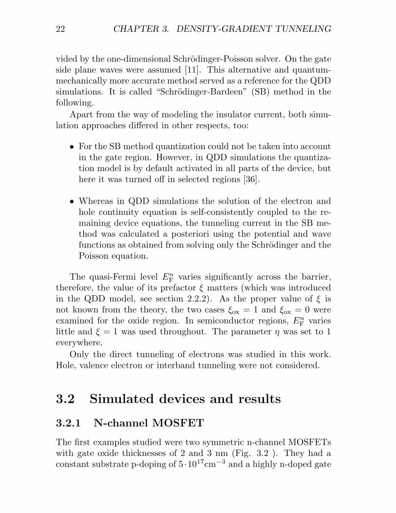
The electron density n and the residual barrier Φ are shown forξox = 0 and ξox = 1 in Fig. 3.6 for three gate voltages that cover theNDR regime. These profiles correspond to the negative branch of thep-doped device in Fig. 3.4. In equilibrium the two cases for ξox areequivalent, but with ceasing inversion they exhibit different profiles inthe oxide as well as in the substrate region next to it. Most striking isthe discontinuity of the density at the oxide-silicon (z = 0) interface
3.2. SIMULATED DEVICES AND RESULTS 27
-0.003 -0.002 -0.001 0 0.001 0.002 0.003z [µm]
-1
-0.5
0
0.5
110
010
210
410
610
810
1010
1210
1410
1610
1810
20d
ensi
ty [
/cm
^3]
VGS = 0 V
VGS = -0.5 V
VGS = -1 V
ξox = 1
ξox = 1
Φ,E
n F[e
V]
-0.003 -0.002 -0.001 0 0.001 0.002 0.003z [µm]
-1
-0.5
0
0.5
110
010
210
410
610
810
1010
1210
1410
1610
1810
20
den
sity
[/c
m^3
]
ξox = 0
ξox = 0
Φ,E
n F[e
V]
Figure 3.6 Simulated electron density n (upper graphs) and effective
band edge Φ (lower graphs) along a MOS diode at different gate voltagesusing ξox = 1 (left part) and ξox = 0 (right part). The structure (from leftto right) is: n+-polysilicon gate, oxide, p-silicon (1018 cm−3). The appliedgate voltages are 0 (equilibrium, thick lines), −0.5 (intermediate) and −1 V(thinnest lines). Note, that the curves in the lower graphs have been shiftedvertically so that they coincide in the gate region. The quasi-Fermi level isincluded as well (dashed lines). The oxide-silicon interfaces are located atz = 0 and −2 nm. The small steps in Φ at the interfaces are due to theDOS discontinuities Φm that are not included in this graph.
for ξox = 0 (upper right graph).2 The reaction of the residual barrieron the applied voltage depends on ξox as well: For ξox = 1 it increases,for ξox = 0 it decreases. This is consistent with the opposite behaviorof the characteristics.
2The discontinuity of the density at the interface on the gate side results fromthe deactivation of QDD inside the gate.

28 CHAPTER 3. DENSITY-GRADIENT TUNNELING
3.2.3 Resonant tunneling diode
NDR is an effect known to occur in resonant tunneling devices (RTDs).The results with the single barrier MOS-structures motivated the in-vestigation of the QDD model applied to silicon RTDs with two SiO2
barriers enclosing a quantum well of varying thickness. The struc-ture is shown in Fig. 3.7. The well is intrinsic and the outer regionsare highly n-doped (1020cm−3). The barriers are 1 nm wide. For allfollowing results ξox =1 was used.
Current characteristics obtained from QDD simulations are shownin Fig. 3.8 (dashed lines). In addition, a curve for a single oxide bar-rier between intrinsic and n-doped silicon is included (circles in Fig.3.8). If the well width of the double-barrier structure is increasedthe behavior approaches that of the single-barrier device which stillexhibits NDR. The occurrence of the QDD current peak and a corre-sponding NDR is related to the dimension of the intrinsic well region.It is present if the well extends over 5 nm or more. For a narrow well,measuring only 1 nm, this effect does not appear (thin dashed line inFig. 3.8).
Furthermore, for the 5-nm structure the NDR-like feature vanishesif the outer regions and also the well are equally n-doped (solid line inFig. 3.8). If the peak would arise from a correct modeling of resonanttunneling this alteration should not completely remove it.
The characteristics for the 1-nm wide, intrinsic well is shown againin Fig. 3.9 (dashed line) compared to the same structure where thedoping was changed to p-type in one of the outer regions (solid line).In the latter a peak in the characteristics and a NDR region reappear,features that are not present in the corresponding symmetrically n+-
1nm 1nm
doped Sidoped Si intr.
Si
SiO
2
SiO
2
Figure 3.7 Structure of a RTD as used in the simulations. The wellconsists of an intrinsic silicon region sandwiched between two SiO2 barriersof 1 nm width.

3.2. SIMULATED DEVICES AND RESULTS 29
−5 −4 −3 −2 −1 0bias [V]
10−10
10−8
10−6
10−4
curr
ent
[a. u
.]
1 nm +n+n i
5 nm +
n+
ni
10 nm +
n+n
i
single barrier +n i
5 nm + n+n+n
Figure 3.8 Currents for RTDs with different well widths calculated withthe QDD model (ξox = 1). The small pictures next to the curves illustratethe device structure. There are three kinds of RTDs: The first ones have anintrinsic well with different widths (dashed lines, white middle regions). Asecond one has an n-doping of 1020 cm−3 also in the well (solid line, shadedmiddle region). The third structure is a single barrier MOS-diode with anintrinsic substrate (•).
doped device. This again indicates that these features are not relatedto resonance effects but rather to an increase of the density differenceacross the barrier.
3.2.4 N-MOSFET off-state leakage
The question to which extent the QDD model may describe the tun-neling contribution to off-state leakage is of great interest for industrialapplication. Therefore, simulations were performed at a fixed source-drain voltage (VDS = 1.2 V) using either the QDD model with ξox = 1,or the Schrodinger-Bardeen approach (Fig. 3.10). For gate voltages

30 CHAPTER 3. DENSITY-GRADIENT TUNNELING
−5 −4 −3 −2 −1 0bias [V]
10−20
10−15
10−10
10−5
100
curr
ent
[a. u
.]
1nm well
+n i p
+ n+n i
Figure 3.9 QDD current characteristics for an RTD with asymmetrical(p-i-n+) doping (solid line) compared to a symmetrically doped device (n+-i-n+, dashed lines). Well and barriers are both 1 nm wide. The negativepotential is applied at the left contact.
larger than 0.5 V the QDD characteristics qualitatively follows theSB reference at a current level lower by almost one decade. Here abetter fit for the ON-state should be obtained by adjusting the oxidemobility. In contrast, the currents differ dramatically in the low andnegative bias region, and in the OFF-state at VGS = 0. This behavioris fully consistent with the earlier observation that the characteristicsare best reproduced if the electron density is high on both sides of thebarrier and that channel depletion is accompanied by the occurrenceof spurious NDR (see results for the MOS-diode and for the MOSFETwith VDS = 0).
It is also striking that the reference model shows a clear positiveshift of the point of zero gate current compared to the QDD result. Atthis point the gate-to-drain tunneling, which is already present in theoff-state, is counterbalanced by an opposite component from sourceto gate that rises with increasing gate potential. The QDD model is

3.3. CONCLUSIONS 31
−0.5 0 0.5 1 1.5VGS [V]
10−11
10−10
10−9
10−8
10−7
10−6
10−5
10−4
10−3
I G [µ
Α]
VDS=1.2V
Schrodinger-Bardeen
QDD ξox = 1
Figure 3.10 N-MOSFET gate leakage current as a function of gatevoltage VGS for a drain voltage of VDS = 1.2 V. The oxide thickness is2 nm. Density gradient results using ξox = 1 (symbols) are compared toSchrodinger-Bardeen (line).
able to reproduce neither the correct position of this point nor thetunneling current in the OFF-state which is a crucial technologicalquantity.
3.3 Conclusions
The QDD model has been used to simulate electron tunneling acrossoxide barriers in silicon MOSFETs, MOS-diodes and RTDs. Themodified model (ξox = 0) produces discontinuous carrier densities, iftunneling occurs from high to low density regions. Non-monotonouscurrent-voltage curves are observed for standard (ξox = 1) QDD simu-lations of single-barrier as well as double-barrier structures. For singlebarriers, however, such a behavior should not be expected; and it isnot seen in the SB reference curves for the MOSFET gate current.This behavior also prevents a qualitative reproduction of the off-state
32 CHAPTER 3. DENSITY-GRADIENT TUNNELING
tunneling current in a MOSFET.The negative differential resistance vanishes if both sides of a bar-
rier are symmetrically n-doped or bias conditions are such that highelectron densities exist on both sides (inversion). Only in this case rea-sonable IV -curves are obtained for the single-barrier devices. Thus,the presence of spurious NDR is related to large density differencesacross the heterostructure.
Particularly for RTDs a NDR-like feature in the QDD simulationdisappears, if all semiconductor regions are equally doped. If therewas a resonance peak, however, symmetric doping would only slightlychange the peak position due to a shift of the bottom of the well.Therefore, the latter is not related to resonant tunneling. The sim-ilarities between single and double barriers also indicate that thesefeatures are not caused by quantum interference. It is also not clearwhether and to what extend the inclusion of the lowest order non-classical correction of the Wigner (or quantum Liouville) equationretains information about the resonance levels.
The reasons for this NDR-artifact and its relation to density dif-ferences are still unclear. Two conjectures shall be mentioned aboutthe failure to describe oxide tunneling:
The gross assumptions that had to be made in the derivation ofthe model – that the potential is a perturbation Φ kT andthat it varies slowly on the length scale of the thermal de-Brogliewavelength – are certainly violated by the band edge step at theSi–SiO2 interface which amounts to 3.2 eV. Nevertheless, thisdoes not prevent the success of QDD in describing quantum me-chanical density profiles at this interface in situations of constantquasi-Fermi level.
In addition, the use of the equilibrium density matrix in itselfis an approximation once it comes to modeling non-equilibrium.Even in describing transport across lower and smoother barrierssuch as the ones present in source-to-drain tunneling (that wassimulated using the same simulation software [33]) similar, albeitweaker NDR features can be observed [37].
One could argue that in the application done here, both approxima-tions, small potential variations and the assumption of being near

3.3. CONCLUSIONS 33
equilibrium, have been violated.Ancona et al. have also applied a modified QDD model to sin-
gle barrier MOS-structures. They distinguish between a dissipativeand a ballistic way of applying the QDD model to tunneling [30, 38].The latter requires that the sum of the kinetic energy gained andthe quasi-Fermi level, the so-called kinetic electro-chemical potential,remains constant across the barrier. As the value of this quantityis tied to the point of origin the tunneling species are split into twopopulations with respect to tunneling direction. Another difference isthe use of Eq. (2.41) instead of introducing the quantum potential asan additional variable. The authors find good agreement to experi-mental tunneling characteristics. The method, however, seems to beinherently restricted to one-dimensional structures.
According to their categories the QDD approach applied in thiswork belongs to the dissipative one: The electron gas is treated as onepopulation for both tunneling directions and a finite mobility is as-signed to the barrier region. Possibly, a nonlocal tunneling treatmentthat retains information about the quasi-Fermi level at the point oforigin could improve the behavior.
Pinnau and Unterreiter apply the QDD model to a GaAs-AlGaAsRTD [39]. They report a “good qualitative agreement with experi-mental measurements” but also that the produced characteristics arevery sensitive to the simulation parameters.
Other authors claim to reproduce resonant tunneling currents byquantum hydrodynamic models [24,40] which include energy balanceequations that are also altered by quantum correction terms. Whetherthese approaches really contain more information about the quantummechanical states that enables the reproduction of resonances remainsto be clarified.
Anyway, this is not the case for the QDD model as it was usedhere. What is also left to examine is the influence of the barrier heightand effective mass. These parameters were not altered in this work.


Chapter 4
RevisedShockley-Read-HallLifetimes for QuantumTransport Modeling
In many modern device simulators the inclusion of quantum effects isstate of the art. However, the main focus is put on the change of thespatial distribution of the carriers by quantum depletion and tunnel-ing effects. Models for quantum mechanical densities mainly comprisesolvers for the Schrodinger equation or density gradient methods. Asthe thus obtained densities are used as input to models for other quan-tities the question arises whether it is sufficient to simply replace theclassical density distributions in these models by quantum mechanicalones, or whether they have to – and how they can be – modeled in amore consistent way.
This chapter deals with this question for the Shockley–Read–Hall(SRH) rate which describes recombination and generation of electronsand holes via deep trap levels in the band gap [41]. This mechanismbelongs to the two most important nonradiative recombination types.The second one is Auger recombination which transfers the energy
35

36 CHAPTER 4. SHOCKLEY-READ-HALL LIFETIMES
of the recombining electron-hole pair to a third carrier.1 New mech-anisms of Auger recombination in quantum wells were theoreticallyidentified by Zegrya et al. [42].
With regard to device simulation, this work presents an examplefor including the QM eigenstates in a model for the Shockley–Read–Hall (SRH) recombination [41]. For one-dimensional confinement, theenergetic separation between the electronic states in conduction andvalence bands and the deep trap levels increases due to subband for-mation. Therefore, in addition to an altered density, it is reasonableto also expect a change of the SRH lifetime in the presence of quan-tization [43].
The model adopted here describes capture and emission of elec-trons between the trap and band states as multiphonon processes,which transfer energy between the electronic and the vibrational sys-tem of the crystal. The corresponding lifetimes receive a spatial de-pendence through the local density of states (DOS) that is composedof the electronic eigenstates in the confining potential. Such an ansatzhas also been used to describe enhanced recombination due to tun-neling as a function of the local electric field [44, 45]. This was doneby accounting for tunnel-assisted transitions, but using densities as inclassical device simulation (without quantum correction).
This chapter is organized as follows: in Section 4.1 the model isintroduced, Section 4.2 presents numerically obtained lifetime profilesfor a simple triangular potential and in Section 4.3 an analytical ap-proximation is derived for the limit of strong quantization. In Section4.4 the model and the approximation are applied to quantum statesresulting from simulated one-dimensional devices.
4.1 Model for the SRH lifetime
4.1.1 Rate formula
SRH recombination occurs via deep trap levels in the energy gap.At first, some quantities that characterize the SRH-recombination areintroduced. This section closely follows the corresponding part in [44].At this stage, the actual mechanism that facilitates the transitions is
1Its counterpart, avalanche generation describes the reverse process.
4.1. MODEL FOR THE SRH LIFETIME 37
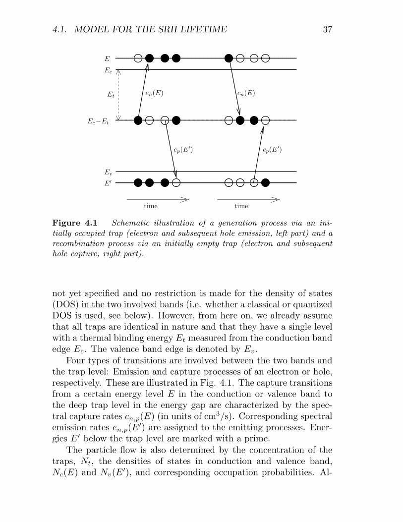
E
E′Ev
Ec
Ec−Et
Etcn(E)
cp(E′)
en(E)
ep(E′)
timetime
Figure 4.1 Schematic illustration of a generation process via an ini-tially occupied trap (electron and subsequent hole emission, left part) and arecombination process via an initially empty trap (electron and subsequenthole capture, right part).
not yet specified and no restriction is made for the density of states(DOS) in the two involved bands (i.e. whether a classical or quantizedDOS is used, see below). However, from here on, we already assumethat all traps are identical in nature and that they have a single levelwith a thermal binding energy Et measured from the conduction bandedge Ec. The valence band edge is denoted by Ev.
Four types of transitions are involved between the two bands andthe trap level: Emission and capture processes of an electron or hole,respectively. These are illustrated in Fig. 4.1. The capture transitionsfrom a certain energy level E in the conduction or valence band tothe deep trap level in the energy gap are characterized by the spec-tral capture rates cn,p(E) (in units of cm3/s). Corresponding spectralemission rates en,p(E′) are assigned to the emitting processes. Ener-gies E′ below the trap level are marked with a prime.
The particle flow is also determined by the concentration of thetraps, Nt, the densities of states in conduction and valence band,Nc(E) and Nv(E′), and corresponding occupation probabilities. Al-

38 CHAPTER 4. SHOCKLEY-READ-HALL LIFETIMES
together they determine the following differential generation and re-combination rates:
drn = Nt cn(E) (1− ft)Nc(E) fc(E) dE (4.1)drp = Nt cp(E′) ft Nv(E′) (1− fv(E′)) dE′ (4.2)dgn = Nt en(E) ft Nc(E) (1− fc(E)) dE (4.3)dgp = Nt ep(E′) (1− ft)Nv(E′) fv(E′) dE′ , (4.4)
where ft is the probability that a trap level is occupied by an electron.Both carrier types are described by their respective quasi-Fermi levels,En
F and EpF, and distribution functions
fc,v(E) =[exp
(E −En,p
F
kT
)+ 1
]−1
. (4.5)
Note that in the rates drp and dgp a simplified description isadopted because no distinction is made between heavy and light holes.The following replacements should be done:
cpNv = clhp N lhv + chhp Nhh
v and epNv = elhp N lhv + ehhp Nhh
v , (4.6)
but we keep the more compact expressions as a shorthand notation[44].
The densities of electrons and holes are given by
n =∫
dE Nc(E) fc(E) and p =∫
dE′Nv(E′) (1−fv(E′)) . (4.7)
In thermodynamic equilibrium detailed balance can be assumed,2
i.e. drn,p = dgn,p, which allows to express the spectral emission ratesthrough the corresponding capture rates:
en(E) = cn(E)(1− f0
t ) f0(E)f0t (1− f0(E))
(4.8)
ep(E′)Nv(E′) = cp(E′)Nv(E′)f0t (1− f0(E′))
(1− f0t ) f0(E′)
. (4.9)
2Otherwise the occupation of a state would change in time.

4.1. MODEL FOR THE SRH LIFETIME 39
Integration over energy yields average capture and emission rates:
cn =∫
dE Nc(E) cn(E) fc(E) (4.10)
cp =∫
dE Nv(E) cp(E) (1−fv(E)) (4.11)
en =∫
dE′ Nc(E′) en(E′) (1−fc(E′)) = cn1− fn
t
fnt
=: cn n1 (4.12)
ep =∫
dE′ Nv(E′) ep(E′) fv(E′) = cpfpt
1− fpt
=: cp p1 , (4.13)
where in the last two lines the relations (4.8) and (4.9) have beenused. The trap occupation probabilities fn,p
t are
fn,pt =
(g exp
(Ec −Et − En,p
F
kT
)+ 1
)−1
, (4.14)
where g is the ratio of the degeneracy factors of the empty and theoccupied trap level. Furthermore, the auxiliary quantities cn = cn/nand cp = cp/p and the densities n1 = n (1−fn
t )/fnt and p1 = p fp
t /(1−fpt ) have been introduced.
Under stationary conditions, the net recombination rate R for elec-trons and holes is equal, R =
∫(drn − dgn) =
∫(drp − dgp) :
cn(1− ft)− enft = cpft − ep(1− ft) , (4.15)
from which ft and, from that, R can be determined:
R = Ntcncp − enep
cn + en + cp + ep= Nt
cncp(pn− n1p1)cn(n + n1) + cp(p + p1)
, (4.16)
where the auxiliary quantities have been used. Reducing with cncpyields two of the usual forms of the SRH-Rate:
R =np− n1p1
τp(n + n1) + τn(p + p1)=
np(1− exp
(Ep
F−EnF
kT
))τp(n + n1) + τn(p + p1)
, (4.17)
with the lifetimes defined as τn = n/(Nt cn) and τp = p/(Nt cp). Allthese quantities may in general depend on the spatial coordinates.

40 CHAPTER 4. SHOCKLEY-READ-HALL LIFETIMES
4.1.2 Capture rate for multiphonon transitions
The capture and emission processes are modeled according to thetheory of multiphonon emission and absorption [46]. The developmentof this theory is beyond the scope of this thesis, it is described in moredetail in [44, 45] and the references therein.
For the purpose of this work the spectral capture and emissionrates are adopted from [44,45]. They are
cn,p(E) = c0n,p
∑l≥0
(l∓S)S
2
L(l) δ(lω0±Ec∓Et∓E) , (4.18)
where the lower signs apply to cp. The trap states are assumed to bestrongly localized and, therefore, to relate only to the carrier densitiesat the same point in space. Furthermore, only a single phonon modeof frequency ω0 is assumed to interact with the electron. The function
L(l) = e−S(2fB
+1)
(fB +1fB
)l/2
Il
(2S√
fB(f
B+1)
)(4.19)
contains the modified Bessel function Il of order l and the Huang–Rhys factor S defining the lattice relaxation energy εR = Sω0. Fur-ther ingredients are the Bose–Einstein occupation probability for thephonon mode with energy ω0, fB = (exp (ω0/kT )− 1)−1 and theenergetic separation Et of the trap levels in the bandgap from thelocal conduction band edge Ec(z). The factor (l∓S)2/S is replacedby unity to avoid the artificial disappearance of the probability ofthermally induced transitions for l = S. As discussed in detail inRef. [45], this artifact is related to the violation of first-order pertur-bation theory when, in a configuration-coordinate diagram, the lowerpotential parabola (bound state) crosses the upper parabola (bandstate) at its minimum, leading to a completely anharmonic lattice po-tential around this crossing point [47]. It should be noted that thefactor does not appear in a two-phonon model with accepting andpromoting modes [48].
We assume that the parameters of the recombination center (Et,S, and εR) are not changed by the confining potential and hence willnot become position dependent. Due to the assumption of a δ-liketrap potential, the influence of the quantum confinement on binding

4.1. MODEL FOR THE SRH LIFETIME 41
energy and wave function of the center is small as long as its distanceto the interface remains larger than its localization radius. However,stronger deviations with respect to the bulk values must be expectedin the case of charged centers with a long-range part of the potential.In addition, alterations of the phonon system (ω0) due to confinementare ignored as well.
From the spectral capture rate one obtains the lifetimes for theelectrons:
τn(z)−1 =Nt c0
n
n(z)
∑l≥0
L(l) Nc(El, z) fc(El) (4.20)
and for the holes:
τp(z)−1 =Nt c0
p
p(z)
∑l≥0
L(l) Nv(El, z) (1− fv(El)) , (4.21)
with
El =
Ec −Et + lω0 for electronsEc −Et − lω0 for holes
(4.22)
where l passes through the number of phonons involved in the transi-tion between trap level and band.
From now on, all considerations are restricted to electrons. Holescan be treated analogously. The spatial dependencies of interest havealready been inserted, namely the z-dependency via the density profileand – which will be the subject of the next sections – via the DOS inthe capture rate cn.
4.1.3 Density of states for quantization in one di-mension
The DOS entering cn is the same as in the densities n and n1. If n isthe quantum mechanical (QM) density, then n1, cn and the lifetimeτn must be treated accordingly. For n1 (and p1) this can be seenimmediately from (4.17): If quantization was not applied consistentlyto n, p and these quantities, then the net rate R would not vanish inthermodynamic equilibrium.

42 CHAPTER 4. SHOCKLEY-READ-HALL LIFETIMES
In the following, quantization of the charge density is consideredonly for the motion along the z axis. The band structure is assumed tobe parabolic with an effective DOS mass m∗ = (mxmymz)1/3 wherethe mi for i = x, y, z are the effective mass tensor components alongthe principal axes. These are chosen to coincide with the Cartesiancoordinate axes for the sake of simplicity.
As mentioned above, quantization affects the lifetimes via the spa-tially varying DOS. The concept of such a “local DOS” and the threecases that are used in the remainder of this chapter are detailed inAppendix A. Here, only the resulting DOS expressions are given:
Without confinement and for vanishing field, the envelope wavefunction consists of plane waves in all three dimensions, and theusual bulk DOS applies:
Nc(E, z) =Mc
2π2
(2m∗
2
)3/2√E−Ec(z) Θ(E−Ec(z)) , (4.23)
where Mc denotes the number of valleys in the conduction band(Mc = 6 in the case of silicon).
For a spatially varying band edge two cases are considered:
In the presence of a homogeneous electric field F in the z-direction (only one classical turning point), Eq. (4.23) is re-placed by
Nc(E, z) =(2m∗
2
)3/2 ∑ν
√θνz2π
F(
Ec(z)−E
θνz
), (4.24)
with the band edge Ec(z) = Ec(0) + eFz, the parameter θνz =(e2F 2/(2mν
z))1/3 and the electro-optical function F as definedin (A.10). This expression contains a non-vanishing DOS con-tribution decaying into the energy gap, as described for the firsttime by Franz and Keldysh for optical absorption in semicon-ductors in a field [49, 50].
For confinement from both sides (two classical turning points)the local DOS contains the wave functions ψνi(z) and eigenen-

4.1. MODEL FOR THE SRH LIFETIME 43
ergies Eνi :
Nc(E, z) =∑ν
mνxy
π2
∑i
|ψνi(z)|2 Θ(E − Eνi) . (4.25)
This DOS corresponds to the density that was already given inEq. (2.11).
In the following, the three different DOS expressions, Eq. (4.23) forplane waves, Eq. (4.24) for a continuous eigenspectrum in a constantfield and Eq. (4.25) for a discrete spectrum, will be referred to as thebulk, the Franz–Keldysh and the quantum-confined DOS (bulk DOS,FKDOS and QCDOS), respectively.
4.1.4 Electron lifetime profiles
Inserting (4.25) into (4.20) yields the electron lifetime
1τn(z)
=
Nt c0n
∑ν
mνxy
∑i
|ψνi(z)|2∑
l≥lνi0 (z)
L(l) fc(El(z))
kT∑ν
mνxy
∑i
|ψνi(z)|2 F0
(En
F −Eνi
kT
) , (4.26)
where lνi0 (z) = max(Eνi−(Ec(z)−Et)
ω0, 0)
is the minimal non-negativenumber of phonons necessary to reach the subband at Eνi from thelocal trap energy given by Ec(z)−Et.
This expression will be further explored in two ways. In section4.2, lifetime profiles are numerically calculated for a triangular poten-tial in order to illustrate the effects of confinement as well as of anelectric field. Secondly, the case of strong confinement (i.e. increasedseparation between the electronic states in the band and the traplevel) is treated analytically in section 4.3. The results will mostly bepresented with respect to the classical lifetime [obtained from (4.20)and (4.23)]:
1τn,cl(z)
=
2 c0nNt
∑l≥Et/ω0
L(l)√
lω0−Et fc(El(z))
√π (kT )3/2 F1/2
(En
F −Ec(z)kT
) , (4.27)
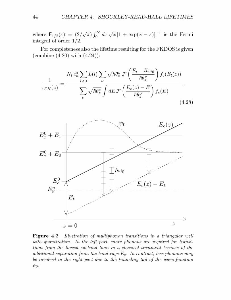
44 CHAPTER 4. SHOCKLEY-READ-HALL LIFETIMES
where F1/2(ε) = (2/√
π)∫∞
0 dx√
x [1 + exp(x − ε)]−1 is the Fermiintegral of order 1/2.
For completeness also the lifetime resulting for the FKDOS is given(combine (4.20) with (4.24)):
1τFK(z)
=
Nt c0n
∑l≥0
L(l)∑ν
√θνz F
(Et − lω0
θνz
)fc(El(z))
∑ν
√θνz
∫dE F
(Ec(z)−E
θνz
)fc(E)
.
(4.28)
E0c + E0
E0c + E1
E0c
EnF
Et
Ec(z)
Ec(z)−Et
z = 0 z
ψ0
ω0
Figure 4.2 Illustration of multiphonon transitions in a triangular wellwith quantization. In the left part, more phonons are required for transi-tions from the lowest subband than in a classical treatment because of theadditional separation from the band edge Ec. In contrast, less phonons maybe involved in the right part due to the tunneling tail of the wave functionψ0.

4.2. LIFETIME PROFILES FOR A TRIANGULAR WELL 45
4.2 Lifetime profiles for a triangular well
In this section a triangular band diagram is considered (Fig. 4.2).The barrier at z = 0 is set to infinite height and for z > 0 a constantelectric field is assumed. The corresponding eigenstates are given inAppendix A (Eqs. A.12 and A.13).
The quasi-Fermi level EnF is assumed to be constant throughout
the system. At z = 0 it lies 0.5 eV below Ec, so that non-degeneratestatistics can be implied safely. In this simple model, the conduc-tion band rises continuously which leads to large separations fromthe quasi-Fermi level at farther distances and is of course unphysical.However, this construction illustrates the transition to field enhance-ment for increasing z.
The lifetimes given by Eqs. (4.26–4.28) were evaluated numer-ically. For the moment, we consider a single valley semiconductor
101
102
103
0 2 4 6 8 10z [nm]
bulk DOS, ω0 = 68 meV
bulk DOS, ω0 = 2 meV
FKDOS, ω0 = 68 meV
FKDOS, ω0 = 2 meV
QCDOS, ω0 = 68 meV
QCDOS, ω0 = 2 meV
τ n(z)c0 nN
t/E
t
Figure 4.3 Comparison of the lifetimes for a triangular well with a fieldstrength F = 5·105 V/cm for different DOS models and two different phononenergies ω0. Thick horizontal lines show the classical lifetime without fieldenhancement or quantum effects. Thin horizontal lines show the results ofusing the FKDOS. The arrows highlight the lifetime reduction due to thefield. The remaining lines indicate the results for the QCDOS including allrelevant eigenstates.

46 CHAPTER 4. SHOCKLEY-READ-HALL LIFETIMES
with isotropic effective mass equal to the longitudinal effective masscomponent ml of silicon. The parameters describing the trap statewere taken from the gold acceptor level in silicon as used in Ref. [45],Et = 0.55 eV, ε
R= 0.238 eV and ω0 = 68 meV. The former were
kept fixed as the phonon energy ω0 was varied. The temperaturewas always T = 300 K. The resulting lifetime profiles are shown inFig. 4.3.
For each subband, the minimum phonon number necessary toreach the trap level changes by one at certain distances from the wall(see Fig. 4.2), which causes a sudden decrease of the lifetime. Theamplitude of these spikes is reduced by choosing a smaller phononenergy. At about 5 nm distance, the lifetime reaches the FK result,which itself is reduced with respect to the bulk value (arrows in Fig.4.3). This reduction is caused by field-enhanced tunneling into thebandgap. In contrast, the steep rise near the wall is caused by theadditional separation of the lowest subband from the trap level dueto quantization.
In the following, the small phonon energy is retained, but the six-fold valley band structure of silicon is used. The coordinate axesare chosen to coincide with the [100]-directions. The following val-ues were used for the effective mass components: longitudinal massml = 0.9163m0 and transverse mass mt = 0.1982m0, where m0 isthe electron rest mass.
Slope and magnitude of the lifetime profile in the part near thewall clearly depend on the field (Fig. 4.4). The curves are more com-plicated because two sets of non-equivalent valleys exist, which havedifferent quantization masses, ml and mt (the latter are labeled withan additional prime on the corresponding subband index). The indi-vidual subband contributions segregate spatially for very high fieldsas the energetic separation of the subband levels increases (Fig. 4.5,for F = 106 V/cm). Near the wall (z < 3 nm), the inverse lifetime isgoverned by the lowest subband of the unprimed set.
The absolute maximum is determined by the lowest primed sub-band because of a larger penetration depth of its wave function intothe bandgap. This maximum, which corresponds to the subband en-ergy E0′ (see Fig. 4.5), is found more than 3 nm beyond the classicalturning point z0′ . Due to the high field the separation between E0′
and the trap level is less than Et/2 at this position, i.e. less than half

4.2. LIFETIME PROFILES FOR A TRIANGULAR WELL 47
0.01
0.1
1
10
100
0 2 4 6 8 10 12
z [nm]
0.01
0.1
1
10
100
0 2 4 6 8 10 12
z [nm]
0.01
0.1
1
10
100
0 2 4 6 8 10 12
z [nm]
τ n/τ n
,cl
τ n/τ n
,cl
τ n/τ n
,cl
F = 105 V/cm
F = 3 · 105 V/cm
F = 6 · 105 V/cm
F = 106 V/cm
Figure 4.4 Lifetime profiles for different field strengths and ω0 = 2 meV(symbols). The Franz-Keldysh lifetime for non-degenerate statistics is givenby dashed lines. The arrow indicates the direction of increasing fieldstrength. Solid lines show an analytical approximation for the contributionof the lowest subband, 1/gQM(z), as defined by formula 4.46 (see below).
of the minimum separation in a classical treatment.Farther from the wall, the primed subbands continue to dominate.
They determine the constant lifetime in the distant part of the profile,which coincides with the corresponding FK result for the given field(dashed lines in Fig. 4.4). This field enhancement reaches a maximumaround 7×10⁵ V/cm for the chosen phonon energy and is reduced forhigher fields (arrow in Fig. 4.4). This non-monotonous behavior canbe understood as follows: With increasing field strength the FKDOSextends into the bandgap and consequently the density increases. Thesum in the numerator of Eq. (4.26), however, is cut off at l = 0 (whichcorresponds to trap-assisted tunneling without phonon assistance).This means that tunneling cannot contribute for energies below thelocal trap level. Thus, in exceeding a certain field strength the increaseof the density prevails and reverses the trend of a decreasing lifetime.
This behavior of the FK lifetime as a function of the field is shown

48 CHAPTER 4. SHOCKLEY-READ-HALL LIFETIMES
10-3
10-2
10-1
100
0 2 4 6 8 10 12 14
z [nm]
0
1
2
0’
1’2’
z0
z0’
total rateml subbandsmt subbands
Et/(τ
nc0 nN
t)
Figure 4.5 Contributions of individual subbands to the inverse lifetimeprofile (circles) as they appear as summands in the numerator of (4.26).Only the respective first three of each set are shown. Primed subband indicescorrespond to the smaller transverse mass mt (dashed lines), unprimed onesto the larger longitudinal mass ml (solid lines). Parameters are F = 106
V/cm and ω0 = 2 meV. The arrows labeled z0 and z0′ indicate the classicalturning points of the lowest subband in each set.
in Fig. 4.6 for different separations between band edge and Fermi levelthat demonstrate degenerate and non-degenerate conditions. Notethat the non-degenerate limit of τn,cl is used for normalization. Be-cause of that the ratio τFK/τn,cl is not unity for En
F Ec and van-ishing field.
The effect of degenerate statistics is illustrated in Fig. 4.7 wherethe Fermi level lies 0.2 eV above the bottom of the triangular well.Near the barrier the FK-lifetime is not constant anymore. Again, itmay reach values greater than unity because the non-degenerate limitof τn,cl is used for normalization.
Note that for a field strength of F = 106 V/cm the differencebetween band edge and Fermi level increases by 0.1 eV with everynanometer. So already for z > 5 nm the separation reaches morethan 1 eV which is due to the construction of this example but would

4.2. LIFETIME PROFILES FOR A TRIANGULAR WELL 49
0 0.5 1F [MV/cm]
10-2
10-1
100
0.2 eV
0
-0.2 eV
-0.4 eV
-0.6 eV
non-
dege
nera
te li
mit
τ FK/τ n
,cl
Figure 4.6 Franz-Keldysh lifetime as a function of the electric field Ffor different values of En
F − Ec which label the curves. If fc(E) is replacedby the Boltzmann distribution in (4.28) the dashed curve is obtained.
0.01
0.1
1
10
100
0 5 10 15
z [nm]
0.01
0.1
1
10
100
0 5 10 15
z [nm]
τ n/τ n
,cl
τ n/τ n
,cl
F = 105 V/cmF = 3 · 105 V/cmF = 6 · 105 V/cmF = 106 V/cm
Figure 4.7 Lifetime profiles as in Fig. 4.4 but for a high Fermi level(En
F = Ec(0) + 0.2 eV), i.e. near the wall the density is degenerate. Thecorresponding Franz-Keldysh lifetime τFK is given by the dashed lines (itsvalue at z = 0 is given by the curve for 0.2 V in Fig. 4.6).

50 CHAPTER 4. SHOCKLEY-READ-HALL LIFETIMES
never occur in real devices. Hence, the non-monotonous behavior ofthe FK lifetime seen in Figs. 4.4 and 4.7 is tied to the extremely non-degenerate case where Boltzmann-statistics is a good approximationeven with DOS contributions deep inside the gap.
4.3 Analytical approximation for strong
quantum confinement
The contribution of a certain subband i at a specified position z isthe stronger the closer it is to the trap energy level and the larger|ψi(z)|2 is. All subbands except the lowest one can be neglected if theconfinement is sufficiently strong to provide a high subband separation( kT ) and if one stays inside or close to the classically allowed region(in Figs. 4.4 and 4.5 this corresponds to z 2 nm). In this case,the probability densities in Eq. (4.26) cancel. Assuming Boltzmannstatistics and defining ζ = 2S
√f
B(f
B+ 1), one obtains
τ−1n =
c0n Nt e−S(2f
B+1)
kT exp(En
F−E0
kT
)×
∑l≥E0−Ec(z)+Et
ω0
Il(ζ) exp(
EnF−Ec(z)+Et−lω0
kT+
lω0
2kT
).
(4.29)
Following Ref. [45], the summation over l is approximated by an in-tegral assuming Et ω0:
τ−1n =
A e∆(z)/kT
ω0
∫∆(z)
dE e−E
2kT IE/ω0(ζ) , (4.30)
where A = c0nNte−S(2f
B+1)/kT and ∆(z) = E0 − Ec(z) + Et denotes
the energetic distance between the local trap level and the lowestsubband energy. In this approximation l = E/ω0 can be regarded aslarge; hence, the modified Bessel function is replaced by its asymptotic
4.3. ANALYTICAL APPROXIMATION 51
form for large order l:
Il(z) →exp
(√l2 + z2 − l ln
(l/z +
√1 + l2/z2
))√
2π√
l2 + z2, (4.31)
yielding
τ−1n =
A e∆(z)/kT
ω0
√2π
∫∆(z)
dE W (E) , (4.32)
with the thermal weight function [45]
W (E) =(
E2
(ω0)2+ ζ2
)− 14
exp
√E2
(ω0)2+ ζ2
− E
ω0ln
(E
ω0 ζ+
√1 +
E2
(ω0 ζ)2
)− E
2kT
.
(4.33)
Assuming high temperature kT ω0, one may use ζ E/ω0
to obtain
W (E) ≈ ω0√2akT
expζ +
a
4kT− (E + a)2
4akT
, (4.34)
where a = (ω0)2ζ/(2kT ) = (εRω0/kT )√
fB (fB + 1). The integralover the Gaussian expression in W (E) produces the complementaryerror function in the result
τ−1n (z) =
c0nNt
2kTC exp
(∆(z)kT
)erfc
(∆(z) + a√
4 a kT
), (4.35)
where C = exp(−ε
R(2f
B+ 1)
ω0+ ζ +
a
4kT
). (4.36)
Now, a is replaced by its high-temperature value a ≈ εR , except in thefactor C, because compensating terms can produce large errors. Ap-plying the asymptotic behavior of the complementary error functionfor large argument [erfc(x) → exp(−x2)/(
√πx)] leads to
τ−1n (z) =
c0nNt C
√εR√
πkT (∆ + εR)
exp
(−EQM
act (Γ(z))kT
). (4.37)
52 CHAPTER 4. SHOCKLEY-READ-HALL LIFETIMES
Hence τn is thermally activated with the activation energy
EQMact (Γ) =
(Et + Γ− εR)2
4 εR
, (4.38)
where Γ(z) = ∆(z)−Et = E0 −Ec(z) is the additional offset betweenthe conduction band edge and the lowest eigenenergy. The barrier forelectron capture is enlarged by the subband offset Γ(z) with respectto the corresponding classical expression, which is E0
act = EQMact (0).
The same form of the thermal activation energy EQMact was used by
Michler et al. in order to deduce the trap energy Et from time-resolvedphotoluminescence experiments on oxygen-doped GaAs-based quan-tum wells of varying widths [51]. They found good agreement with in-dependent bulk measurements of a presumably damage-induced deeplevel.
The classical lifetime (4.27) can be treated in a similar manner.For Boltzmann statistics and small phonon energy one obtains
τ−1n,cl(z) =
BeEt/kT
ω0
∫Et
dE e−E/2kT IE/ω0(ζ)
√E −Et
kT
≈ BeEt/kT
ω0
√2π
∫Et
dE W (E)
√E −Et
kT, (4.39)
with B = 2 c0n Nte−S(2f
B+1)/(
√πkT ). Applying the high temperature
approximation as before leads to
τ−1n,cl(z) ≈
c0n Nt C
π√
a (kT )3/2
∫Et
dE exp[w(E)] , (4.40)
with the same C as defined in (4.36) and
w(E) = −(E + a)2
4akT+
12ln(
E − Et
kT
).
As in Ref. [45] the integral is approximated by expanding w around its

4.3. ANALYTICAL APPROXIMATION 53
maximum at the dominant transition energy E∗, yielding the formula∫ ∞
Et
dE exp[w(E)]
≈ exp(w(E∗))√
π
2|w′′(E∗)| erfc(√
|w′′(E∗)|2
(Et − E∗)
).
(4.41)
From w′(E∗) = 0, one finds
E∗ ≈ Et +akT
Et + a, (4.42)
w(E∗) ≈ −(Et − a)2
4akT− Et
kT+
12ln(
a
Et + a
), (4.43)
w′′(E∗) ≈ −(Et + a)2
2(akT )2, (4.44)
which gives the following result for the lifetime (replacing a by εR):
τ−1n,cl(z) ≈
erfc(−1
2
)c0nNt C ε
R√πkT (Et+εR)3/2
exp(−E0
act
kT
). (4.45)
With the results (4.35) and (4.45), a “quantum correction” factor withrespect to the zero-field classical SRH lifetime can be defined:
gQM(z) :=τn,cl
τn≈√
εR+Et
εR
exp
(E0
act−EQMact (z)
kT
)erfc
(−12
) , (4.46)
where the z-dependence outside the exponents has been neglected(∆ ≈ Et). The remaining exponential contains the difference of theactivation energies (compare Ref. [45]).
As long as the contribution of the lowest subband dominates thelifetime, this approximation works very well, in case of the triangularpotential for sufficiently high fields and z 2 nm (Fig. 4.4). The case∆ = 0 marks the classical turning point where gQM is of the order ofunity, with the parameters used here.
The calculation of gQM still requires the knowledge of the eigenen-ergy E0 of the lowest subband, in order to calculate the local value

54 CHAPTER 4. SHOCKLEY-READ-HALL LIFETIMES
of ∆. However, E0 may not be explicitly available, for example if thedensity gradient model is used to account for quantization. In thesecases E0 can at least be obtained in the lowest subband approximationfrom formula (2.11) by expressing the dominating probability densityas |ψ0(z)|2 = n(z)/
∫n(z) dz:
E0 = EnF − kT F−1
0
(π
2
2 kTmxy
∫n(z) dz
). (4.47)
For a device simulator, the problem would consist in choosing anappropriate interval for integrating the density. In addition, the deviceregions must be determined where expression (4.46) is a sufficientapproximation.3
4.4 Lifetime profiles for simulated devices
Up to this point, a very simple potential shape has been assumed. Inorder to study more realistic situations, the input for calculating thelifetime profile (band edges, quasi-Fermi energies, eigenenergies, andwave functions) was taken from DESSIS−ISE device simulations [36]that solved the coupled system of the Poisson equation and the conti-nuity equations. In all examples the relaxation energy εR = 0.238 eVwas retained regardless of the material and Et was chosen such thatthe trap level is located in the middle of the band gap.
4.4.1 Metal-oxide-semiconductor diode
A MOS diode with a p-doped silicon substrate (1018 cm−3), stronglyn-doped silicon gate (1020 cm−3) and an oxide width of 2 nm was sim-ulated using the self-consistent Schrodinger-Poisson solver [11]. Quan-tization was considered for electrons only. Direct tunneling throughthe oxide and SRH recombination were enabled [5]. For this sim-ulation, constant SRH lifetimes were used (τ0
n ≈ 9.9 × 10⁻⁸ s andτ0p ≈ 2.97× 10⁻⁸ s). The simulated charge profiles are shown in Fig.4.8. From the results of this simulation a new electron lifetime profile
3In a MOS inversion layer, this region may be much smaller than reasonableintegration intervals.

4.4. LIFETIME PROFILES FOR SIMULATED DEVICES 55
was calculated using a phonon energy of ω0 = 2 meV (Fig. 4.8, rightaxis). The lifetime decreases by almost four orders of magnitude fromthe wall to the minimum located 8 nm away. This corresponds tothe behavior already analyzed for the triangular potential. It is wellreproduced by the lowest subband approximation within the first 3nm. Beyond the minimum, the lifetime increases and reaches a con-stant value at z ≈ 50 nm. This can be explained by the ceasing fieldenhancement effect as the field strength decreases towards the end ofthe space-charge region.
In the MOS diode, the SRH recombination rate is only influencedby the field enhancement in the space charge region. The strongincrease near the oxide has no effect because the hole density is verysmall there.
0.01
0.1
1
10
100
0 10 20 30 40 50
100
105
1010
1015
dens
ity [c
m-3
]
z [nm]
electron density
hole density
1/gQM
τ n/τ n
,cl
Figure 4.8 Profiles of the electron and hole density (dashed lines, rightaxis), the electron lifetime τn (symbols) and lowest subband approximationfor τn using E0 from expression (4.47) (solid line). The horizontal dottedline indicates the zero field lifetime.

56 CHAPTER 4. SHOCKLEY-READ-HALL LIFETIMES
4.4.2 Quantum-well diode
The simulated structure corresponds to an intrinsic GaAs quantumwell between two layers of Al0.4Ga0.6As that form a pin diode. The p-and n-doping of the AlGaAs regions is 1017 cm−3. Spherical parabolicbands are used for electrons and holes, with an electron effective massof m∗
e = 0.0672m0 and two hole effective masses: mlh = 0.0485m0
and mhh = 0.407m0. Furthermore, a single constant c0p for heavy and
light holes is assumed (cf. (4.21)).Two well widths were considered: 30 and 5 nm. The Schrodinger
equation was solved for both carrier types in a region containing theGaAs well and a few nanometers of the adjacent material. In the
10101011101210131014101510161017
-1.5
-1
-0.5
0
0.5
dens
ity [c
m-3
]
Ec
[eV
]
a)
electrons (Ec)
holes (Ev)
0.1
1
10
100
-15 -10 -5 0 5 10 15z [nm]
b) electrons (30nm)
holes (30nm)
electrons (5nm)
holes (5nm)
τ/τ c
l
Figure 4.9 See next page for caption

4.4. LIFETIME PROFILES FOR SIMULATED DEVICES 57
1019
1020
1021
1022
-15 -10 -5 0 5 10 15
SR
H r
ate
[1/s
/cm
3 ]
z [nm]
c) with τcl
with τ(z)
Figure 4.9 Carrier density (a), lifetime (b) and SRH rate profiles (c)at 1V forward bias inside two quantum wells of different widths (30 nm and5 nm, to be discerned by the different plot ranges along z). Subfigure a:Simulation results for the conduction and valence band edges (right axis)and the carrier densities as calculated from the eigenstates (left axis). Sub-figure b: Ratio of the quantum-confined (QC) and bulk lifetime, τ and τcl,for both electrons (filled symbols) and holes (open symbols). Lines indicatethe lowest subband approximation 1/gQM(z) with E0 obtained from formula(4.47). Subfigure c: SRH rate obtained with constant lifetimes (τ0
n = 10−8 sand τ0
p = 10−9 s, dash-dotted lines) and with the QC lifetime profile fromsubfigure b after multiplying by τ0
n,p (solid lines).
simulations, constant SRH lifetimes were used: τ0n = 10−8 s and τ0
p =10−9 s, for electrons and holes, respectively. Results are presentedfor 1 V forward bias. Band edges and carrier densities are shown inFig. 4.9a, the resulting lifetime profiles in Fig. 4.9b for ω0 = 2 meV.One can observe differences with respect to the confinement lengthand carrier type. For the 30-nm well, the electron lifetime shows adistinct field reduction in the left part of the well, corresponding tohigher subbands, and an increasing slope towards the right wall. Bothfeatures are far less pronounced in the hole lifetime profile. This canbe explained by the dominance of the heavy-hole band. The light-holeband does not contribute much because its in-plane DOS is smaller.

58 CHAPTER 4. SHOCKLEY-READ-HALL LIFETIMES
In the narrow well (5 nm), the electron lifetime is considerablyhigher than in the wide well. For the hole lifetime this is not thecase. The crucial parameter is the shift of the lowest subband withshrinking well width. The heavy hole subband is not lifted much withrespect to the minimum potential (regarding hole energies), but theelectron subband is.
The numerical lifetime profiles are compared with the lowest sub-band approximation (4.46). They agree very well for the electronsin the narrow structure and least for the holes in the wide structure(Fig. 4.9b). The deviations illustrate the limitation of this formulato large subband separations, i.e. small quantization mass and strongconfinement.
The change of the SRH rate upon replacing the constant SRH life-times with the calculated profiles is shown in Fig. 4.9c. For all ratesthe QM densities are used. The ratio of the trap level degeneracyfactors in (4.5) is set to g = 1. The 30-nm structure shows an over-all increased rate. The enhancement reaches a factor of 2 and moretowards the left end of the well. The maximum increases by approx-imately 70 %. The rate in the 5-nm structure is reduced, mainly inthe left half of the well. The maximum decreases by about 70 %.
Of course, the impact of the spatially varying lifetimes on therate is controlled by the densities and by τ0
n,p: The electron lifetimeτn is multiplied by the hole density p in (4.17). As p is small com-pared to the electron concentration the replacement by the quantum-mechanically consistent lifetime is only of minor importance althoughit is increased by more than an order of magnitude.
By changing the doping of the pin-structure, however, it is possibleto reverse the situation. Fig. 4.10 shows the densities, lifetimes andrates for a p-doping of 1018 cm−3 and an n-doping of 1015 cm−3.The quantum well is located in the middle of a 100-nm wide intrinsicregion. As now the electrons govern the rate because of their smallconcentration the effect of lifetime enhancement is carried forward.Inside the narrow well the rate is reduced by a factor of 30 comparedto the use of classical lifetimes. In the wider well the rate is slightlyreduced, too.
Reduced nonradiative capture rates due to confinement were alsofound by Delerue et al. in a theoretical study of recombination in smallsilicon crystallites [52]. Jursenas et al. examined the recombination of

4.4. LIFETIME PROFILES FOR SIMULATED DEVICES 59
1010
1012
1014
1016
-15 -10 -5 0 5 10 15de
nsity
[cm
-3]
a)
electronsholes
1
10
100b) electrons (30nm)
holes (30nm)
electrons (5nm)
holes (5nm)
τ/τ c
l
1017
1018
1019
1020
-15 -10 -5 0 5 10 15
SR
H r
ate
[1/s
/cm
3 ]
z [nm]
c)
with τcl
with τ(z)
Figure 4.10 Same structure as in Fig. 4.9 but the doping of the p andn-regions is changed in a way that leads to a higher hole density and fewerelectrons in the wells (a). Also the field in the well region is lower so thatno lifetime reduction due to field enhancement occurs (b). Using the QClifetimes instead of the constant ones reduces the SRH-recombination rateaccording to the increase of the electron lifetime (c).

60 CHAPTER 4. SHOCKLEY-READ-HALL LIFETIMES
photo-excited hot carriers in CdS nanocrystals [53]. The multiphononcontribution was divided into an interface and a volume channel withdifferent activation energies. The authors state, however, that theparticle size was too large to see confinement effects; the observed sizedependence was attributed to the changing surface-to-volume ratio.
4.5 Conclusions
The SRH lifetime has been modified to consistently account for quan-tization effects. The model combines a local DOS composed of theeigenstates of the system with multiphonon recombination processes.Strongly localized traps and a single phonon energy are assumed. Themodel has been investigated for small phonon energies (Et ω0).The results exhibit two effects:
On one hand, the electric field may enable tunneling of the wavefunction, which enhances the capture and emission processes andthus reduces the lifetime.
On the other hand, the additional separation of the lowest sub-band from the band edge can cause a considerable increase ofthe lifetime. For this effect, an analytical approximation hasbeen derived. The form of the activation energy is supported byan earlier experiment [51].
Note that the recombination in the barriers of a quantum wellwas not considered nor any other nonradiative channels for carrierloss such as thermionic escape. The latter causes an increasing non-radiative contribution with decreasing well width [54], in contrast torecombination within the confined structure, as was considered here.
Modified lifetimes have been computed for quantized carriers inone-dimensional devices:
In a MOS diode, the quantization leads to enhanced recombi-nation in the depletion layer due to the electric field, but thesubband offset near the oxide barrier is of no importance.
The lifetimes in a GaAlAs-GaAs-based quantum well diode havebeen studied as well. In a wide well the model may feature both

4.5. CONCLUSIONS 61
an increase and a reduction of the lifetime if the field is strongenough to enable both quantum confinement in the lower partof the well and field enhanced recombination in the other parts.
In a narrow well of 5 nm width the subband separation is strongenough to increase the electron lifetime by more than an orderof magnitude. For holes this effect is much less important dueto their higher effective mass. These conditions can cause areduction of the SRH rate if the density proportions favor thedominance of the electron lifetime.
Including these effects may be of importance for the modeling ofsmall confining structures, e.g. quantum-well devices or thin siliconfilms. To this end, a model for both quantum-confinement and field-enhancement effects would be desirable. A drawback in this respectmay be the nonlocal form of the analytical “quantum correction” fac-tor gQM that requires the knowledge of the lowest eigenenergy E0.


Chapter 5
Quantum-MechanicalModeling of theLow-Field DriftMobility in MOSDevices
The drift mobility is a very important transport coefficient in semicon-ductor devices. Several scattering mechanisms such as scattering byphonons, interface asperities and charged impurities impede the flowof charge carriers in an electric field and thus determine a finite valueof the mobility. In a MOS transistor the drift mobility is a criticalparameter because it determines the on-current.
Quantization is of importance not only for the shape of the den-sity profile but one also has to account for the fact that the initialand final states of the scattering processes differ from the bulk situa-tion. Moreover, the quantization of the mobile charge in the channel(and elsewhere) also affects the way they screen external perturbationswhich is important for the treatment of impurity scattering.
In this chapter, a model for the mobility is described which takes
63
64 CHAPTER 5. QUANTUM-MECHANICAL MOBILITY
into account the one-dimensional quantization of the charge carriersin the direction perpendicular to the confining interface or transportplane. As before, this is chosen to be the z-axis. The model is based onthe quantum mobility model in the device simulator DESSIS−ISE thatincludes electron-phonon and interface roughness (IR) scattering andwas fitted to reproduce the universal mobility curve.
Main object of the work presented here is to add the contributionof Coulomb scattering by ionized impurities which are important forlow inversion sheet densities or effective fields (see next section fordefinitions). In doing so, the inclusion of screening by the mobilecharge in the channel is the crucial ingredient. In a second step themodel is extended in order to assess the effect of impurities in thepolysilicon gate of a MOS structure. These remote charges have beenconsidered important in the case of very thin gate oxides. But on theother hand, the gate region is also the source of additional screeningdue to its high concentration of mobile carriers.
This chapter is organized as follows: Section 5.1 presents some in-troductory remarks about the definition of the measurable “effective”quantities. The calculation of the effective mobility in the frameworkof the relaxation time approximation is outlined in section 5.2. Themodeling of the individual scattering mechanisms is subject of thefollowing three parts. The Coulomb part is divided into screeningeffects and the treatment of impurity fluctuations, which constitutethe actual sources of scattering. In section 5.6 the mobility model isapplied to simulated MOS structures with thin gate oxides.
5.1 Effective mobility extraction
Experimentally the inversion layer mobility of a MOSFET is obtainedfrom measuring the channel current Ich (at either source or drain con-tact) and the inversion charge Qinv per unit area [55]. The latterstems from integrating the gate-to-channel capacitance which is ob-tained from a “split CV” measurement [56,57]. The effective mobilityis defined from the linear current-voltage relationship for the outputcharacteristics:
µeff =Ich
WL VDS |Qinv|
. (5.1)

5.1. EFFECTIVE MOBILITY EXTRACTION 65
For this formula to be valid, the measurements have to be carried outat a low driving field, i. e. the electric field parallel to the insulator-semiconductor interface, F‖, must be sufficiently small, requiring asufficiently long channel, typically several microns, and the source-to-drain voltage VDS must be small. Eq. (5.1) can be converted into aweighted average of the mobility profile:
µeff =∫
dz n(z)µ(z)∫dz n(z)
, (5.2)
where the weight function is the density profile n(z). This expressionis more convenient for a calculation of µeff from device simulationdata.
Mobility measurements are commonly presented as the relationµeff(Eeff), where Eeff , the normal effective field, was originally definedas [58]
Eeff =∫
dz n(z)F⊥(z)∫dz n(z)
, (5.3)
where F⊥(z) is the normal electric field with respect to the confin-ing interface or transport plane. But instead of (5.3) the followingdefinition is used:
Eeff =Qdepl + η Qinv
εSi, (5.4)
where εSi is the permittivity of silicon. The depletion charge per unitarea, Qdepl, is calculated assuming a constant substrate doping Nsub
and using the depletion approximation: QDAdepl =
√4 e εSi Nsub φf with
φf = kT/e ln(Nsub/ni). This expression for Eeff is motivated by theexperimental findings that, for an appropriate choice of the parameterη, the effective mobility curves µeff(Eeff) for different doping concen-trations fall on top of each other to yield a “universal mobility” [59].Eq. (5.4) is actually obtained from (5.3) with η = 1/2 under the(in general good) assumption that the inversion layer is much thin-ner than the depletion layer [58]. However, this value only holds forelectrons and for a (100)-orientation of the Si-SiO2 interface. For(110) and (111)-orientations as well as for p-type conduction a valueof η = 1/3 had to be used in (5.4) in order to produce a universalbehavior [59, 60].

66 CHAPTER 5. QUANTUM-MECHANICAL MOBILITY
For thin gate oxides a gate leakage current IG arising from directtunneling complicates the measurement of the mobility. The draincurrent ID is not identical to the source current IS any more and thechannel current Ich in (5.1) is not simply equal to either one of them.In general, its value should vary along the channel. The problem ofgate leakage becomes more critical for long-channel devices. On theother hand, however, low-field mobility measurements require thatthe channel is not too short. Some authors suggest to use the averageIch = (IS + ID)/2 [61,62], others present an estimate for the error ofthis approach [63].
5.2 Relaxation time approximation
This section follows the usual solution of the linearized Boltzmannequation [64]. But in case of quantization in the z-direction, in con-trast to bulk material, a Boltzmann equation can be formulated foreach subband with respect to the remaining two dimensions [65]. As-suming that in each subband n the distribution function fn only de-pends on the two-dimensional wave vector κ (spatial homogeneity),one obtains the following equation:
− e
F · ∇κfn(κ) =
∑n′
∑κ′
[S(nκ|n′κ′)(1− fn(κ))fn′(κ′)
−S(n′κ′|nκ)(1− fn′(κ′))fn(κ)].
(5.5)
The equations for different subbands are coupled via the scatteringterms. The transition probability from state (nκ) to (n′κ′) is denotedby S(n′κ′|nκ). For low electric field F the equation is linearized withthe usual ansatz:
fn(κ) = f0(En(κ)) +d
dEf0(En(κ)) eF‖ ·Λn(κ) , (5.6)
where f0 is the equilibrium distribution, En(κ) = En + Eκ and Eκ
is the kinetic energy of the motion in the plane perpendicular to theinterface. From comparing the coefficients of the first order in the

5.2. RELAXATION TIME APPROXIMATION 67
electric field one obtains an equation for the group velocity:
vn(κ) =∑n′κ′
S(n′κ′|nκ)1− f0(En′(κ′))1− f0(En(κ))
(Λn(κ)−Λn′(κ′)) . (5.7)
A scalar relaxation time τn is introduced by the ansatz Λn(κ) =vn(κ) τn(Eκ). This is possible in the following two cases:
1. The scattering is elastic and S only depends on the absolutevalue of the wave vector difference q = |κ − κ′|.
2. S only depends on the energies and subband indices of the in-volved states.
The first case will be applied to Coulomb and IR scattering and thelatter will be used to treat the electron-phonon scattering. The scat-tering probabilities are obtained from Fermi’s golden rule.
In the case of elastic scattering no energy is lost or gained, thus Shas the form
S(n′ν′κ′|nνκ) =2π|Mn
n′νν′(κ,κ′)|2 δ(En′(κ′)−En(κ)) . (5.8)
From here on, the subband index will be accompanied by an additionalindex ν, indicating the valley. The matrix element of the perturbationis denoted by Mn
n′νν′(κ,κ′) for transitions from state (nνκ) to (n′ν′κ′).
The band structure is assumed to be parabolic and isotropic so thatvnν = κ/mν
xy with mνxy =
√mν
xmνy . Then, from (5.7) the following
set of coupled equations is obtained for the relaxation times [66, 67]:
1τnν(E = Eν
κ)=∑n′ν′
(Ann′
νν′(E)−Bn
n′νν′(E) τn′ν′(Enν −En′ν′ + E)
τnν(E))
,
(5.9)where
Ann′
νν′(E) =
LxLymν′xy
π3
∫ π
0
dϑ |Mnn′
νν′(q)|2 (5.10)
and
Bnn′
νν′(E) =
LxLymνxy
π3
√mν′
xy(E+Enν−En′ν′)mν
xy E∫ π
0
dϑ |Mnn′
νν′(q)|2 cosϑ .
(5.11)

68 CHAPTER 5. QUANTUM-MECHANICAL MOBILITY
These expressions still contain the normalization lengths Lx,y, whichwill cancel once an explicit formula for the matrix element is used.The matrix element only depends on q = |κ − κ′| = 2κ sin(ϑ/2),where ϑ is the angle between the vectors κ and κ′.
If inter-subband transitions are neglected, i.e. (n′ν′) = (nν) thissystem simplifies to
1τnν(Eν
κ)=
LxLymνxy
π3
∫ π
0
dϑ |Mnnνν(q)|2(1− cosϑ) . (5.12)
In the second case, Eq. (5.7) is solved by the relaxation time
1τnν(Eν
κ)=
∑n′ν′κ′
S(Enν(κ)|En′ν′(κ′))f0(En′ν′(κ′))f0(Enν(κ))
. (5.13)
5.2.1 Drift mobility
The current density profile in the nth subband and νth valley is givenby
jnν(z) = q nnν(z) vDnν = 2 q |ψnν(z)|2
∫d2κ
(2π)2fnν(κ)vnν(κ) , (5.14)
wherennν(z) =
2LxLy
|ψnν(z)|2∑κ
fnν(κ) (5.15)
and
vDnν =
∑κ fnν(κ) vnν(κ)∑
κ fnν(κ)(5.16)
are the corresponding density profile (including spin) and mean driftvelocity.
The distribution function is replaced by the low-field approxima-tion (see (5.6)):
fnν(κ) = f0(Enν(κ))
− qβ f0(Enν(κ))(1−f0(Enν(κ))
)τnν(Eν
κ)vnν(κ) · F‖(5.17)
where f0 is the Fermi function and β = 1/kT . The relaxation timeaccounts for all scattering mechanisms considered here:
τnν =((τPhon.
nν )−1 + (τCoul.nν )−1 + (τSurf.
nν )−1)−1
. (5.18)

5.2. RELAXATION TIME APPROXIMATION 69
The resulting two-dimensional ohmic conductivity tensor is
σ(z) = 2 q2β∑nν
|ψnν(z)|2∫
d2κ
(2π)2f0(Enν(κ))
× (1−f0(Enν(κ))
)τnν(Eν
κ)vnν(κ)⊗vnν(κ) .
(5.19)
For cubic symmetry of the crystal (e.g. for unstrained silicon) andcoordinate axes along the [100]-directions the conductivity tensor isdiagonal and the two diagonal components are equal, so it can bedescribed by a scalar. Here, the xx-component is selected to representits value. The integral is rewritten as∫
dE f0(E)(1−f0(E)) τnν(E)∫
d2κ
(2π)2δ(E − Eν
κ) (vxnν(κ))2 . (5.20)
From calculating the average of the velocity square on a line of con-stant energy one obtains
σ(z) =∑nν
|ψnν(z)|2 q2β
π
√mν
y
mνx
∫dE τnν(E)f0(E)(1−f0(E)) (1 + αE) E
1 + 2αE︸ ︷︷ ︸=:gnν
(5.21)where gnν is the conductance per subband and valley. This formulastill contains the non-parabolicity factor α [14] which will be set tozero in the following.
With (5.2), the effective mobility becomes the sum of all subbandconductances per sheet density:
µeff =1
qNs
∑nν
gnν
∫channel
dz |ψnν(z)|2 . (5.22)
In general, the integral should be one because the wave functions arenormalized. But usually they penetrate the insulating barrier, andthat part is considered not to contribute to the current, which resultsin values slightly smaller than one.

70 CHAPTER 5. QUANTUM-MECHANICAL MOBILITY
5.3 Coulomb scattering
The electrons in a MOS channel scatter at immobile charges like ion-ized impurities, as well as oxide fixed charges or charged interfacestates which all will be called impurities in the following. Thesecharges are considered as an external perturbation of the alreadysolved system. Their actual contribution to the perturbed Hamil-tonian is their Coulomb potential which is screened by the responseof the mobile carriers.
The next section describes methods to calculate the screened Cou-lomb potential. After that, the treatment of the impurity density andthe way to obtain the norm square of the matrix element are discussed.
5.3.1 Screening
Basic theory
The potential V of a given charge density ρ is the solution of thePoisson equation. After 2D-Fourier transformation in the in-planecoordinates x‖ = (x, y) it reads
(∂zε(z)∂z − q2ε(z))V (q, z) = −ρ(q, z) , (5.23)
where
V (q, z) =∫
d2x‖ exp(−iq · x‖) V (x‖, z) . (5.24)
The solution for V (q, z) is expressed with the help of a Green’s func-tion (see Appendix B):
V (q, z) =∫
G(q, z, z′)ρ(q, z′)dz′ . (5.25)
The coordinates z′ and z are the positions of the source and the probeof the potential, respectively.
For bulk material, i.e. constant ε, G is given by (B.7). Its func-tional form becomes more complicated, if there is more than one re-gion with different ε. The expressions for up to three layers of differentdielectrics are given in Appendix B.
5.3. COULOMB SCATTERING 71
In the case of Coulomb scattering the charge density ρ is composedof two components:
ρ(r) = ρext(r) + ρind(r) , (5.26)
the “external” impurity charge and the resulting induced charge due tothe reaction of the mobile carriers which gives rise to screening. Thisinduced charge is approximated by first order perturbation theory(r = (x‖, z)):
ρind(r) = −e∑n νn′ν′
∑q
Lnn′
νν′(q)V n
n′νν′(q)ψ∗
n′ν′(z)ψnν(z) exp(iq · x‖) ,
(5.27)
where Lnn′
νν′(q) is the polarization factor (see Appendix C) and V n
n′νν′(q)
is the scattering matrix element of the potential for the scattering vec-tor q = κ′ − κ:
V nn′
νν′(q) =
−e
LxLy
∫dz ψ∗
n′ν′(z)V (q, z)ψnν(z) . (5.28)
Plugging the Fourier transform of the induced charge
ρind(q, z) = −eLxLy
∑n νn′ν′
Lnn′
νν′(q)V n
n′νν′(q)ψ∗
n′ν′(z)ψnν(z) (5.29)
into (5.25) and using (5.28) results into an integral equation for thepotential V :
V (q, z) =∫
dz′ G(q, z, z′)ρext(q, z′)
+ e2∑n νn′ν′
Lnn′
νν′(q)
∫dz V (q, z)ψ∗
n′ν′(z)ψnν(z)
×∫
dzG(q, z, z)ψ∗n′ν′(z)ψnν(z) .
(5.30)

72 CHAPTER 5. QUANTUM-MECHANICAL MOBILITY
Solving the integral equation
Now a potential φ(q, z, z′) is introduced which is defined as a Green’sfunction with respect to the external perturbation ρext(q, z) only:
V (q, z) =∫
dz′ φ(q, z, z′)ρext(q, z′) . (5.31)
Inserting this relation into (5.30) yields
V (q, z) =∫
dz′ G(q, z, z′)ρext(q, z′)
+∫
dz′ ρext(q, z′)∫
dz φ(q, z, z′)
× e2∑n νn′ν′
Lnn′
νν′(q)ψ∗
n′ν′(z)ψnν(z)∫
dzG(q, z, z)ψ∗n′ν′(z)ψnν(z)
︸ ︷︷ ︸=:K(q,z,z)
,
(5.32)
which is solved if φ satisfies an own integral equation:
φ(q, z, z′) =∫
dz K(q, z, z)φ(q, z, z′) + G(q, z, z′) . (5.33)
This equation can be solved using the Nystrom method [66,68]. Whenthis is done, V can be constructed using (5.31) and the scatteringmatrix elements (5.28) can be computed.
The method for obtaining the scattering potential is similar tothe one presented in [66]. What is different here, however, is theGreen’s function which already reflects the dielectric layering of thestructure [69,70] and the use of a q-dependent polarization factor [65]instead of a screening constant in the long-wavelength limit [6] (seebelow). Other authors solve equations corresponding to (5.30) byapplying iterative schemes [69, 71].

5.3. COULOMB SCATTERING 73
Matrix elements from inverting the dielectric tensor
An alternative path to the matrix elements is to construct them simplyaccording to (5.28) from (5.30) (cf. Ref. [65]):
V mm′
µµ′(q) = (Vext)mm′
µµ′(q) +
∑n νn′ν′
V nn′
νν′(q)
× Lnn′
νν′(q) e2
∫dz ψ∗
m′µ′(z)ψmµ(z)∫
dzG(q, z, z)ψ∗n′ν′(z)ψnν(z)︸ ︷︷ ︸
=:F nn′ν
ν′ mm′
µ
µ′ (q)︸ ︷︷ ︸=:χ n
n′νν′ m
m′µ
µ′ (q)
.
(5.34)
The first term is the matrix element of the “external” potential Vext
which stems from the term containing ρext in (5.30):
(Vext)mm′µµ′(q) =
−e
LxLy
∫dz ψ∗
m′µ′(z)ψmµ(z)
×∫
dz′ (−e)G(q, z, z′)ρext(q, z′) .
(5.35)
The second term can be cast into a product of the susceptibility ten-sor χ with the matrix element of V . This, in turn, consists of thepolarization factor and the form factor F , which is an overlap integralover both spatial arguments of the Green’s function with the wavefunctions.
Rearranging the terms, the dielectric function ε can be identified,which relates the screened matrix elements (containing V ) to the un-screened ones (containing Vext):
(Vext)mm′µµ′(q) =
∑n νn′ν′
(δmnδm′n′δµνδµ′ν′ − χ n
n′νν′
mm′
µµ′(q)
)︸ ︷︷ ︸
=: ε nn′ν
ν′ mm′
µ
µ′ (q)
V nn′
νν′(q)
(5.36)
By inverting the tensor ε, the screened matrix elements can be ob-tained. Note that this formalism, naturally, only relates matrix ele-ments built with one set of quantum states. Therefore, only screeningby the inversion charge itself can be taken into account.
74 CHAPTER 5. QUANTUM-MECHANICAL MOBILITY
Remote Coulomb effects
So far the considerations were restricted to quantum states in thechannel only. However, in MOS structures with thin gate insulatorsone can imagine that charges on either side of the insulator influ-ence each other by Coulomb forces. For example, impurity charge inthe gate could cause additional scattering of the mobile carriers inthe channel. This is commonly called “remote Coulomb scattering”(RCS).1 In addition to that, the mobile charge in the gate can causeadditional screening, due to an induced charge reacting to the “exter-nal” charges on either side. An appropriate name for this effect wouldbe “remote screening”.
In order to formulate the induced charge on the other side of theoxide (typically in a polysilicon gate) it is assumed that 1D wavefunctions are known also for that part of the device. In the following,a simple structure consisting of materials A, B, and C is considered.
The insulating barrier material is denoted by B, the channel regionby C, and A is the gate region added to the consideration above. Theinterfaces are located at zAB and zBC (see Fig.5.1). Both regions Aand C contain a quantum region for which a separate set of 1D wavefunctions and eigenenergies is available. Under bias these regions havedifferent Fermi potentials, too.
In analogy to (5.29) the induced charge due to a perturbing po-tential V is
ρCind(q, z) ∝∑n νn′ν′
(LC)nn′νν′(q)V n
n′νν′(q)ψC∗
n′ν′(z)ψCnν(z) , for z > zBC
1Often it is also named “remote charge scattering”.
z
A B C
zAB zBC
Figure 5.1 Two separate quantum regions, indicated by the dashed pat-tern.

5.3. COULOMB SCATTERING 75
and
ρAind(q, z) ∝∑n νn′ν′
(LA)nn′νν′(q)V n
n′νν′(q)ψA∗
n′ν′(z)ψAnν(z) , for z < zAB .
For the moment we assume that in the insulating region there is noinduced charge (ρBind = 0). The equation for φ then has two contribu-tions:
φ(q, z, z′) =∫z<zAB
dz KA(q, z, z)φ(q, z, z′)
+∫z>zBC
dz KC(q, z, z)φ(q, z, z′) + G(q, z, z′) .
(5.37)
The kernel functions KA,C can be extended with zeros to cover thesame domain and then be added to yield a single function. This way,an equation of the type (5.33) is obtained where z and z cover the samerange. This is important for the Nystrom method where a quadraticmatrix is needed [68].
In case of wave functions penetrating the barrier, the integrationlimits zAB and zBC in (5.37) have to be replaced by values lying insidethe barrier. This corresponds to a non-vanishing contribution of ρBind.
2
Approximations
In practice the sum over the subbands and valleys is further simplified.In the calculations of this work inter-valley contributions to screen-
ing are neglected in the induced charge (5.27). This is justified by theBloch factors in different valleys. For two valleys that are centeredaround k0 and k′
0, respectively, these give rise to a rapidly oscillatingfactor exp(±i(k0 − k′
0)r) which lets the inter-valley matrix elementsvanish [65, 72]. This approximation corresponds to replacing the po-larization factor by Ln
n′νν′(q) ≈ Ln
n′νν(q) δν,ν′ .
Several authors [66,69,71] only include diagonal contributions (nointer-subband screening) and use the long–wavelength limit (C.17):
2In principle, one could also consider the case that the quantum regions overlapinside the barrier. But this would require some interpolation in order to add upthe kernel function if the grid in both boxes was different.
76 CHAPTER 5. QUANTUM-MECHANICAL MOBILITY
Lnn′
νν′(q) ≈ Ln
nνν(0) δν,ν′δn,n′ which reduces the induced charge density
(5.29) to
ρind(q, z) = 2∑n,ν
Snν |ψnν(z)|2∫
dz′ V (q, z′) |ψnν(z′)|2 , (5.38)
with the screening parameter [6]
Snν =e2
2π2mν
xy f(Enν) . (5.39)
5.3.2 Fluctuations of the impurity density
Being provided with the relation between the the screened potentialV (q, z) and the external charge density ρext(q, z), now an expressionfor the latter is needed.
The number density of the impurity charges is given by
N3D(r) =Ntot∑i=1
δ(r− ri) , (5.40)
where Ntot is the total number of impurities. This number density isapproximated by areal densities N2D
t (x‖) in layers which are perpen-dicular to the z-direction [65]. Each impurity is assigned to one of Tlayers by the function L and the z-coordinates of all impurities in thetth layer are approximated by zt:
N3D(r) =Ntot∑i=1
δ(x‖−xi) δ(z−zi) ≈Ntot∑i=1
δ(x‖−xi) δ(z−zL(i)) , (5.41)
where r = (x‖, z), ri = (xi, zi) and L(i) = t, for zt − wt/2 ≤ zi <zt +wt/2 (wt is the width of layer t). This can be rewritten as a sumover all layers and the impurities in each layer (thus the index i isrestricted to the impurities in layer t):
N3D(r) =T∑t=1
Ntot∑i=1,
L(i)=t
δ(x‖ − xi) δ(z − zt) =:∑t
N2Dt (x‖) δ(z − zt) ,
(5.42)

5.3. COULOMB SCATTERING 77
where N2Dt (x‖) is defined as the sum over all δ(x‖ − xi) for which zi
lies within the tth layer. The positions ri of the impurities are dis-tributed according to a probability distribution P (r1, . . . , rNtot
). Thestatistical average of the density is given by
〈N3D(r)〉 =∫
d3r1 . . .
∫d3rNtot
P (r1, . . . , rNtot) N3D(r) . (5.43)
Now, this average density is assumed to be invariant under transla-tions by a vector b in the x‖-plane:
〈N3D(x‖, z)〉 = 〈N3D(x‖ + b, z)〉 (5.44)
which means that it is a constant with respect to x‖:
〈N3D(z)〉 = 1LxLy
∫d2x‖〈N3D(x‖, z)〉 . (5.45)
Using the layer approximation (5.41) in this expression, the deltafunction in the in-plane coordinates replaces xi by x‖:
〈N3D(z)〉 ≈ 1LxLy
Ntot∑i=1
δ(z − zL(i))∫
dz1 . . .
∫dz
Ntot
×∫
d2x1 . . .
∫d2x‖ . . .
∫d2x
NtotP (x1, z1, . . . ,x‖, zi, . . . ,xNtot
, zNtot
)
(5.46)
The integral is unity due to the normalization of the probability dis-tribution. What remains is
〈N3D(z)〉 ≈∑t
Nt
LxLyδ(z − zt) =
∑t
〈N2Dt 〉δ(z − zt) , (5.47)
where Nt is the number of impurities in the tth layer.The mobile carriers are scattered by the spatial inhomogeneities
in the impurity potential. Therefore, the density that gives rise to thescattering is given by the fluctuations δN3D of the impurity densityaround its statistical average:
δN3D(r) = N3D(r)− 〈N3D(z)〉 ≈∑t
δN2Dt (x‖) δ(z − zt) , (5.48)
where the layer approximation is used and δN2Dt (x‖) = N2D
t (x‖) −〈N2D
t 〉.

78 CHAPTER 5. QUANTUM-MECHANICAL MOBILITY
Final expression for the norm square of the matrix element
With (5.48) the total scattering potential V as given by (5.31) becomes
V (q, z) = qimp
∑t
φ(q, z, zt) δN2Dt (q) , (5.49)
δN2Dt (q) =
∫d2x‖ δN2D
t (x‖) exp(−iq · x‖) , (5.50)
where qimp is the charge of one impurity. Then the matrix elementand its norm square are
V nn′
νν′(q) = qimp
∑t
δN2Dt (q)φn
n′νν′(q, zt) , (5.51)
|V nn′
νν′(q)|2 = q2
imp
∑s,t
(δN2D
s (q))∗
δN2Dt (q)
× (φnn′
νν′(q, zs))
∗φnn′
νν′(q, zt) ,
(5.52)
with [in analogy to (5.28)]
φnn′
νν′(q, zt) =
−e
LxLy
∫dz ψ∗
n′ν′(z)φ(q, z, zt)ψnν(z) . (5.53)
Still, the Fourier transform of the fluctuations δN2Dt is not known, as
neither is the exact location of the impurities. Therefore, the statis-tical average is taken. For the sake of simplicity it is assumed thatthe positions xi of the impurities in different layers are uncorrelated.Then, on average, all terms with s = t vanish:
|V nn′
νν′(q)|2 = q2
imp
∑t
⟨∣∣δN2Dt (q)
∣∣2⟩ |φnn′
νν′(q, zt)|2 . (5.54)
The statistical average of the power spectrum of the density fluctua-tions can be further decomposed [73]:⟨|δN2D
t (q)|2⟩ =⟨|N2D
t (q)|2⟩− (LxLy)2〈N2Dt 〉2δq,0 . (5.55)
Apart from a normalization,⟨|δN2D
t (q)|2⟩ is the static structure fac-tor. It is determined by the spatial correlations among the impurities

5.3. COULOMB SCATTERING 79
within a layer. Here, it is assumed that the distribution of the impu-rities is totally random, i.e. P (xi) is constant with respect to thexi. This leads to [73]⟨|N2D
t (q)|2⟩ = Nt + δq,0Nt(Nt − 1) (5.56)
and ⟨|δN2Dt (q)|2⟩ = LxLy〈N2D
t 〉(1− δq,0) . (5.57)
With this assumption (5.54) becomes
|V nn′
νν′(q)|2 = q2
impLxLy(1− δq,0)∑t
⟨N2D
t
⟩ |φnn′
νν′(q, zt)|2 (5.58)
≈ q2impLxLy(1− δq,0)
∫dz
⟨N3D(z)
⟩ |φnn′
νν′(q, z)|2 (5.59)
where the sum over the layers has been replaced by an integrationover the direction perpendicular to the interface. Note, that the Kro-necker symbol may be dropped because q = 0 is reached only forintra-subband scattering, where the (1− cosϑ)-term in (5.12) alreadyensures that the inverse relaxation time vanishes.
Correlations among the impurity charges have been neglected inthis work. They can be included based on hard sphere exclusion bothfor different charges within the same layer [73] and also between dif-ferent layers [74]. In the latter case the sign of the charges becomessignificant. In modeling the effect of oxide charges the neglect of botheffects may amount to an underestimation of the total effective mobil-ity by 15% according to Ref. [74] as scattering is then overestimated.On the other hand the hard sphere radius in this model has to beregarded as a fitting parameter.
Inter-valley scattering
Up to this point inter-valley transitions (ν = ν′) have still been in-cluded in the formulas. However, in the actual numerical calculationsthe corresponding matrix elements are neglected and only intra-valleymatrix elements are taken into account for Coulomb scattering. Cor-respondingly, Eqs. (5.9–5.11) are used for the case ν = ν′ only. Thisapproximation can be justified for valleys that differ in the in-plane

80 CHAPTER 5. QUANTUM-MECHANICAL MOBILITY
wave vectors κ and κ′ because then |q| is large [66,69]. At these highspatial frequencies the Fourier components of the potential and theenvelope wave function are small.3
5.4 Interface roughness
The normal component F⊥ of the electric field attracts the carrierstowards the insulator-semiconductor interface. A carrier that passesalong this interface experiences a changing influence which gives riseto scattering. The underlying spatially varying properties of the in-terface are commonly figured as the roughness of the interface. Thus,the actual interface is modeled as a defined border between the twomaterials that varies around a mean position. In this picture the de-viations from this mean position, the roughness fluctuations, give riseto the scattering. The difficulty consists in determining the actualperturbation Hamiltonian associated with these fluctuations.
Consider a system consisting of an insulator with an effective massmins and a semiconductor with ms separated by an interface at z = 0.The unperturbed Hamiltonian is
H = −2
2∂
∂z
1m(z)
∂
∂z+ΦBΘ(−z) + U(z) , (5.60)
where m(z) = minsΘ(−z) + msΘ(z) and the confining potential issplit into the electrostatic potential energy U = qϕ and the bandedge jump ΦB at the insulator barrier. In the perturbed case, theinterface at position x‖ is shifted to z = ∆(x‖), i.e. it is described bythe coordinates (x‖,∆(x‖)). In principle all parts in (5.60) cause acontribution to the perturbing Hamiltonian. The kinetic part
δT = −2
2∇(
1mins
− 1ms
)(Θ(z)−Θ(∆(x‖)− z)
)· ∇ (5.61)
which is due the step in the effective mass is seldom mentioned in theliterature [11]. It can be neglected as the typical kinetic energies are
3Note that this argument fails for silicon with a [100]-oriented interface fortransitions between the two valleys with longitudinal quantization mass. However,there still exists the argument with the Bloch factors (see above, page 75).

5.4. INTERFACE ROUGHNESS 81
much smaller than ΦB which gives rise to
δΦB = ΦB
(Θ(∆(x‖)− z)−Θ(−z)
). (5.62)
In addition, there exists a contribution qδϕ because on one hand thedielectric constant changes between z = 0 and ∆(x‖) and on the otherhand the whole perturbation induces a response δρ of the charge den-sity which self-consistently determines the shift δϕ in the electrostaticpotential. Wettstein developed an iteration scheme for obtaining aself-consistent solution for δϕ but in the actual implementation theuse of the induced density δρ has been turned off in order to obtainresults that can be fitted to the experimental data of Takagi et al. [11].
For the sake of readability the index pair nν is substituted by i inthe following. Then, the band edge jump contribution to the matrixelement is
δΦBii′(q) =
1LxLy
∫d2x‖ exp(−iq · x‖) Iii′(x‖) , (5.63)
with
Iii′(x‖) = ΦB
∞∫−∞
dz ψ∗i′(z)ψi(z)
(Θ(∆(x‖)−z)−Θ(−z)
). (5.64)
Substituting z by z + ∆ in the first step-function and expanding thewave functions around z yields
Iii′(x‖) = ∆(x‖)ΦB
∞∫−∞
(∂ψ∗
i′
∂zψi +
∂ψi
∂zψ∗i′
)Θ(−z) dz +O(∆2) .
(5.65)The step-function sets the upper integration limit to zero. Then, theSchrodinger equation
ΦBΘ(−z)ψi(z) =(Ei − U(z) +
2
2∂
∂z
1m(z)
∂
∂z
)ψi(z) (5.66)
can be used for z < 0, so Θ(−z) is unity and m(z) = mins. Integration

82 CHAPTER 5. QUANTUM-MECHANICAL MOBILITY
by parts leads to
Iii′(x‖) = ∆(x‖)
([ψi ψ
∗i′(Ei′ − U)
]0
−∞+[
2
2mins
∂ψi
∂z
∂ψ∗i′
∂z
]0
−∞
+
0∫−∞
dz ψi∂U
∂zψ∗i′ + (Ei − Ei′)
0∫−∞
dz∂ψ∗
i′
∂zψi
)+O(∆2) .
(5.67)
If the band edge step is sufficiently large, so that the wave functioncan be neglected for z ≤ 0, the following term survives:
Iii′(x‖) ≈ ∆(x‖)
2
2mins
∂ψi
∂z
∂ψ∗i′
∂z
∣∣∣∣z=0
. (5.68)
Often the mass step is disregarded [75–77]. Then, all masses arereplaced by a constant effective mass m in (5.66) and (5.68) that iscommon to the barrier and the semiconductor region. This is theresult of Prange and Nee [75].
Wettstein uses another approximation of (5.64):
Iii′(x‖) ≈ ΦB
∆(x‖)2∆0
∆0∫0
dz ψ∗i′(z)ψi(z) , (5.69)
where ∆0 is the amplitude of the roughness [11]. This expressionshould be more accurate than the one resulting from a simple “ex-pansion” of the step function Θ(∆− z) ≈ Θ(−z) + δ(−z)∆:
Iii′(x‖) ≈ ΦB ∆(x‖)ψ∗i′(0)ψi(0) . (5.70)
According to Matsumoto and Uemura [78] the effect of the irregular in-terface can approximately be described by the potential ∆(x‖) ∂U/∂zwhich implies
Iii′(x‖) ≈ ∆(x‖)∫
dz ψi∂U
∂zψ∗i′ . (5.71)
A similar expression can actually be obtained from (5.65) by using

5.4. INTERFACE ROUGHNESS 83
the Schrodinger equation (5.66) before applying the step function:
Iii′(x‖) = ∆(x‖)
(
2
2
∞∫−∞
dz
(∂
∂z
1m(z)
)∂ψi
∂z
∂ψ∗i′
∂z
+
∞∫−∞
dz ψi∂U
∂zψ∗i′ + (Ei − Ei′)
∞∫−∞
dz∂ψ∗
i′
∂zψi
)+O(∆2) .
(5.72)
This equation states that (5.71) is valid only for constant mass andi = i′.4 In the electric quantum limit (i.e. only the lowest subband isoccupied) this directly provides a simple dependence on the effectivenormal field: I0
0(x‖) = q Eeff∆(x‖).All approximations have in common that the perturbation depends
linearly on the interface displacement: Iii′ = ∆ · Mnn′
νν′ . Therefore,
the square of the matrix element of IR scattering has the form
|Mnn′
νν′(q)|2 = C(q) |Mn
n′νν′ |2 , (5.73)
where C(q) = |∆(q)|2/(LxLy)2 is the spectrum of the interface corre-lation function
C(x‖) =1
LxLy
∫d2x ∆(x)∆(x+ x‖) . (5.74)
An exponential decay of the roughness fluctuations given by C(x‖) =∆2
0 exp(−√2 |x‖|/Λ) with the roughness amplitude ∆0 and the corre-
lation length Λ corresponds to the spectrum [79]
C(q) =π∆2
0Λ2
LxLy(1 + q2Λ2/2)3/2. (5.75)
Screening
Up to this point only the band edge step has been considered. Thecontribution of the change δϕ in the electrostatic potential is stillmissing. Following Ref. [11], but neglecting the change in the dielectric
4It corresponds to the fact that the average force∫ |ψi|2 ∂Ec
∂zdz vanishes for a
bound state.

84 CHAPTER 5. QUANTUM-MECHANICAL MOBILITY
constant, the corresponding induced charge density is, in analogy to(5.29),
ρind(q, z) = −eLxLy
∑i,i′
Lii′(q)
(ΦB
ii′(q) + Vind
ii′(q)
)ψ∗i′(z)ψi(z) ,
(5.76)where the matrix element of the induced potential itself is
Vindii′(q) =
−e
LxLy
∫dz ψ∗
i′(z)δϕind(q, z)ψi(z) . (5.77)
The band edge step is either given by (5.63) or by
δΦBii′(q) =
−e
LxLy
∫dz ψ∗
i′(z)δϕB(q, z)ψi(z) , (5.78)
where it is assumed that formally an “artificial” potential δϕB cor-responding to the band edge step can be formulated. An exampleis
δϕB(x‖, z) =∆(x‖)−e
∂V
∂z, (5.79)
which corresponds to (5.71).Everything is done in a similar manner as in section 5.3.1. A
difference, however, is the fact that δϕB is not an external electrostaticpotential in the sense that any external charge density is associatedwith it (which would turn up on the right hand side of the Poissonequation). Therefore, here, the auxiliary quantity φ connects the totalpotential δϕtot = δϕind + δϕB to the artificial potential δϕB ratherthan to an external charge:
δϕtot(q, z) =∫
dz′ φ(q, z, z′) δϕB(q, z′) . (5.80)
By expressing the induced electrostatic potential with the help ofGreen’s function, i.e.
δϕind(q, z) =∫
G(q, z, z′)ρind(q, z′)dz′ , (5.81)
and using (5.76) and (5.80) one obtains, in analogy to (5.33),
φ(q, z, z′) =∫
dz K(q, z, z)φ(q, z, z′) + δ(z − z′) , (5.82)

5.4. INTERFACE ROUGHNESS 85
where the screening kernel K is the same as defined in (5.32) (replacenν by i).
However, there are cases for which no such artificial potential func-tion δϕB(z) can be found, e. g. for (5.68) and (5.69). Then, as in sec-tion 5.3.1, the screened matrix element is obtained using the inverseof the dielectric function ε:
δΦBii′(q) :=
∫dz δϕtot(q, z)ψi(z)ψ∗
i′(z) =∑j,j′
(ε−1)ii′jj′(q) δΦB
jj′(q) .
(5.83)
Thus, the screening of the IR perturbation works the same way asfor the Coulomb potential.
Inter-valley transitions are neglected as in the case of Coulombscattering.
Note that first order perturbation theory enters the treatment ofIR and Coulomb scattering in two places: The first is the formulationof the perturbation Hamiltonian. There is a reaction of the chargedensity which is part of the perturbation itself but also depends on it.Thus, self-consistency is required. The induced density consists of thefirst order corrections of the wave functions (see (5.27) and (5.29)).The second one is the use of Fermi’s golden rule, i.e. first order timedependent perturbation theory.
A different model for IR scattering was developed by Ando [76,77].It uses a perturbation Hamiltonian which does not include a first or-der density correction but, instead, uses the difference δn between theunperturbed density profile n(z) and a displaced one, n(z − ∆(x‖)):δn(z) ≈ −∆∂n(z)/∂z. This density correction causes a potentialδφn =
∫G(q, z, z′) δn(z′) dz′. Matrix elements are then calculated
from a perturbation consisting of δφn, the band edge jump displace-ment (5.62) and other contributions that treat dipole moments arisingfrom the deformed interface. These matrix elements are then subjectto screening by dividing them by a scalar dielectric function. Thismodel is quite commonly used in the literature [80–83]. Neverthe-less, it remains unclear how the particular choice of the perturbation(which is inconsistent with a first order treatment) can be justified.

86 CHAPTER 5. QUANTUM-MECHANICAL MOBILITY
5.5 Phonons
The model for the electron-phonon scattering has been adopted from[11]. The interaction of the electrons with the acoustic phonons isdescribed as an intra-valley scattering process in the elastic approxi-mation as the change in energy is small.
In addition, the dispersion relation is assumed to be linear (Debyemodel): ω(q) = c q, where c is the velocity of sound. A single defor-mation potential constant Dac is used to describe the interaction withthe electrons. For the acoustic phonons the Bose-Einstein occupationnumber is approximated as fBE(ω(q)) ≈ kT
ω(q) − 12 .
The optical phonons give rise to inter-valley scattering. For theirdispersion relation the Einstein model is used, i.e. a single mode offrequency ω. Two different deformation potential constants, Df andDg, are applied for inter-valley f - and g-scattering, respectively.
For a parabolic band structure the relaxation times are then givenas [11]
1τacnν(E)
=D2
acmνxy
2ρ c2
∑n′
αn′ν,nνΘ(Enν + E −En′ν) (5.84)
and
1τ intnν (E) =
∑λ=±1
∑ν′ =ν
λfBE(λω)f(Enν + E − ω)
f(Enν + E)
× (Dintνν′)2mν′
xy
22ρω
∑n′
αn′ν′,nνΘ(Enν + E − En′ν′ − ω) ,
(5.85)
where ρ denotes the mass density of the silicon crystal and
αn′ν′,nν =∫
dz|ψn′ν′(z)|2|ψnν(z)|2 (5.86)
are overlap integrals of the wave function squares. The parameterDint
νν′ in (5.85) represents either Df or Dg, depending on the valleysinvolved.

5.6. RESULTS 87
5.6 Results
The wave functions and eigenenergies were obtained from device simu-lations with DESSIS−ISE using its 1D-Schrodinger solver which is self-consistently coupled to the Poisson equation [15,27]. The Schrodingerequation was solved in an interval reaching from a few Angstroms in-side the oxide to some 10 nanometers into the channel region. Thisregion is called quantum region in the following. In order to includethe screening effect of the gate electrons a second quantum region wasnecessary that covered the nearest 5 to 20 nm of the polysilicon gate.
The actual mobility calculation as described in this chapter tookplace outside DESSIS−ISE . It was implemented in MATLAB [84].
5.6.1 Effective field
In Fig. 5.2 the effective field Eeff is shown as a function of Ninv =Qinv/e for two substrate dopings. Three different definitions of theeffective field are compared:
1. Eq. (5.4) for η = 1/2 with the fixed value for QDAdepl from the
depletion approximation (dashed lines)
2. Eq. (5.4) for η = 1/2 with Qdepl as obtained from the simulation(solid lines)
3. Eq. (5.3) (dashed-dotted lines)
If calculated from the simulation data the depletion layer chargeQdepl varies as a function of the applied gate voltage and can fall belowthe analytical value of QDA
depl (see section 5.1) if Qinv is small. In thiscase a sub-threshold branch can be seen in the simulated mobilitycurves which is not present in experimental diagrams (Fig. 5.2, lowergraph). Definition 2 is used in the following. Above threshold thedifferences are relatively small.
5.6.2 Depth of the gate quantum region
Bound eigenstates can be computed for the quantum region in thechannel. In the quantum region on the gate side, however, there isno confining potential well as on the substrate side. So, in principle,there should be a continuum of states.

88 CHAPTER 5. QUANTUM-MECHANICAL MOBILITY
105
106
108 109 1010 1011 1012 1013
Eef
f [V
/cm
]
Ninv [1/cm2]
3e17
2.4e18
(QDAdepl + η Qsim
inv )/εSi
(Qsimdepl + η Qsim
inv )/εSi
Eq. (5.3)
102
103
105 106
mu e
ff [c
m2 /V
s]
Eeff [V/cm]
exp. data
(QDAdepl + η Qsim
inv )/εSi
(Qsimdepl + η Qsim
inv )/εSi
Eq. (5.3)
Figure 5.2 Upper graph: Effective field as a function of the inversionlayer sheet density Ninv for different definitions (see text). Lower graph:Effective mobility plotted versus the different effective fields compared toexperimental data of Ref. [59] (oxide thickness of 25 nm).

5.6. RESULTS 89
But as the Schrodinger solver imposes a boundary condition onthe “free” end of the quantum region, it returns a set of discretelevels. The energetic distance of these “quasi-bound” levels is mainlydetermined by the depth DG
z of the quantum region in the gate.5 Thelarger DG
z the more and closer lying eigenstates are obtained. On onehand it is important to work with a sufficient number of these stateswhich requires a quantum region that is sufficiently large. On theother hand this increases the computational effort as more subbandshave to be taken into account in the gate.
As the boundary conditions have been designed for the case ofbound states, unphysical density profiles arise at the “free” end of thequantum region in the gate. In addition, intricate convergence issuesof the simulator were found to restrict the width of the quantum regionto somewhere below 10 to 20 nm especially for high substrate dopings( 1017cm−3) and larger oxide thicknesses ( 5 nm).
A first criterion to decide whether a certain depth of the gatequantum region is sufficiently large is to compare the electron densityprofiles in the gate region. As expected, the electron density decreasesstrongly directly at the oxide interface due to the quantum depletioneffect (Fig. 5.3). As the gate voltage increases, the electrons retreatfurther from the oxide interface. Around the “free” end of the quan-tum region the boundary condition causes an unphysical drop of thedensity profile where it should be constant instead. A depth of 4 nmis obviously too short to settle the profile at the constant bulk density.
5.6.3 Screened Coulomb potential
The screened potential of the remote charges in the gate is illustratedin Figs. 5.4–5.6 for selected distances from the gate oxide interface.They show the potential φ(q, z, z′) for two selected wave numbersq and some positions z′ of the source charge. These positions areidentified by the peak value of the potentials and are located 10, 5, 3,2 and 1.5 nm away from the oxide-substrate interface. The depth ofthe quantum region in the gate is DG
z = 20 nm. Two effects can beobserved with rising gate voltage:
5This depth is not the total width Lz of the quantum region which is larger bythe additional depth it penetrates into the gate oxide.

90 CHAPTER 5. QUANTUM-MECHANICAL MOBILITY
0
0.2
0.4
0.6
0.8
1
1.2
-14 -12 -10 -8 -6 -4 -2
n(z)
[1e2
0/cm
3 ]
z [nm]
-0.5 V
2 V20nm8nm4nm
Figure 5.3 Electron density profile for different depths DGz of the quan-
tum region in the gate (DGz = 4, 8 and 20 nm) shown for two different gate
voltages VG = −0.5 and 2 V. The oxide thickness is tox = 1 nm, substrateand gate doping are 1018 and 1020 cm−3, respectively. Vertical dashed linesindicate the borders of the two shorter quantum regions.
0
2
4
6
8
10
12
14
-12 -10 -8 -6 -4 -2 0 2 40
0.2
0.4
0.6
0.8
1
1.2
1.4
1.6
1.8
V(q
,z)
[Vm
2 /As]
n(z)
[1e2
0/cm
3 ]
z [nm]
q=1.54e5/cmq=2.37e7/cm
density
0
2
4
6
8
10
12
14
-12 -10 -8 -6 -4 -2 0 2 40
0.2
0.4
0.6
0.8
1
1.2
1.4
1.6
1.8
V(q
,z)
[Vm
2 /As]
n(z)
[1e2
0/cm
3 ]
z [nm]
0
2
4
6
8
10
12
14
-12 -10 -8 -6 -4 -2 0 2 40
0.2
0.4
0.6
0.8
1
1.2
1.4
1.6
1.8
V(q
,z)
[Vm
2 /As]
n(z)
[1e2
0/cm
3 ]
z [nm]
Figure 5.4 Density profile and screened potentials for two values of q at
VG ≈ −0.19 V, below the onset of inversion. DGz = 20 nm.

5.6. RESULTS 91
0
2
4
6
8
10
12
14
-12 -10 -8 -6 -4 -2 0 2 40
0.2
0.4
0.6
0.8
1
1.2
1.4
1.6
1.8
V(q
,z)
[Vm
2 /As]
n(z)
[1e2
0/cm
3 ]
z [nm]
q=1.54e5/cmq=2.37e7/cm
density
0
2
4
6
8
10
12
14
-12 -10 -8 -6 -4 -2 0 2 40
0.2
0.4
0.6
0.8
1
1.2
1.4
1.6
1.8
V(q
,z)
[Vm
2 /As]
n(z)
[1e2
0/cm
3 ]
z [nm]
Figure 5.5 As above in Fig. 5.4. VG ≈ 0.13 V, weak inversion.
0
2
4
6
8
10
12
14
-12 -10 -8 -6 -4 -2 0 2 40
0.2
0.4
0.6
0.8
1
1.2
1.4
1.6
1.8
V(q
,z)
[Vm
2 /As]
n(z)
[1e2
0/cm
3 ]
z [nm]
q=1.54e5/cmq=2.37e7/cm
density
Figure 5.6 As above in Fig. 5.4. VG = 2 V, strong inversion.

92 CHAPTER 5. QUANTUM-MECHANICAL MOBILITY
The component of the potential with the longer wavelength in-creases once the source of it comes to lie within the widening deple-tion region. Being surrounded by less electronic charge the screeningof these components becomes less effective.
However, the tail of the potential that actually reaches into thechannel region is reduced. This is can be explained by the screeningof the inversion charge that builds up in the channel. The componentwith the shorter wavelength remains almost unaffected by screening.
Qualitatively, the increase of remote charge in the depleted gateregion seems to be compensated by the screening by the inversioncharge.
5.6.4 Coulomb-scattering-limited mobility
The effective mobility is presented as a function of the effective fieldfor different oxide thicknesses tox =0.5, 1, 2, 5, and 25 nm. The depthof the gate quantum region has been reduced to 8 nm in order to keepit the same for all thicknesses. Only Coulomb scattering (CS) is takeninto account, for the moment.
Before including any effects from the gate region (remote chargescattering and remote screening) only the impurities in the substrateare considered as sources of scattering and only the screening fromthe inversion charge is taken into account. A constant p-doping con-centration of 1018 cm−3 is used in expression (5.59). All curves forthe different oxide thicknesses lie on top of each other, with exceptionof the sub-threshold part (Fig. 5.7). The mobility starts to rise ateffective fields between 5 · 105 and 5.5 · 105 V/cm.
Now only the remote impurities in the gate are taken into account.However, the mobile electrons on both sides of the oxide contribute toscreening. The thus obtained RCS-limited mobility strongly dependson the oxide thickness (Fig. 5.8). For oxide thicknesses of 5 nm andmore it surmounts 105 cm2/Vs and one would not expect any influenceonto the overall mobility.
Fig. 5.9 shows the effect of remote screening for the case that themobility is again limited only by substrate impurity scattering. Thesub-threshold mobility of all curves is increased with respect to Fig.5.7, even for the largest oxide thickness.

5.6. RESULTS 93
103
104
106
µ eff
[cm
2 /Vs]
Eeff [V/cm]
0.5nm1nm2nm5nm
25nm
Figure 5.7 Coulomb-scattering-limited effective mobility due to scatter-ing from the substrate impurity potential screened by the channel inversioncharge. Various oxide thicknesses, substrate p-doping: 1018 cm−3.
102
103
104
105
106
107
108
109
1010
106
µ eff
[cm
2 /Vs]
Eeff [V/cm]
0.5nm1nm2nm5nm
25nm
Figure 5.8 CS-limited effective mobility due to remote charge scatteringfrom the gate impurities. Screening by gate and channel electrons. The gateis n-doped with a concentration of 1020 cm−3.

94 CHAPTER 5. QUANTUM-MECHANICAL MOBILITY
103
104
106
µ eff
[cm
2 /Vs]
Eeff [V/cm]
0.5nm1nm2nm5nm
25nm
Figure 5.9 Same as in Fig. 5.7, but with additional screening by theelectrons in the gate.
If now the screening and scattering charges from both sides of theoxide are taken into account a more complex behavior arises (Fig.5.10). At high effective fields there is a reduction of the mobility withdecreasing oxide thickness. This reduction is not seen for thicknessesof 5 nm and more.
In the sub-threshold regime the mobility has a maximum for acertain oxide thickness, in the region of 1 to 2 nm. Two effects workagainst each other: As the oxide thickness decreases, the sources ofremote screening and scattering move closer to the channel region.The former tends to increase the mobility while the latter reduces it.
Altogether, a thinner oxide reduces the slope of the CS-limitedmobility curve reaches above the inversion point. Therefore, the so-called “Coulomb roll-off” of the overall mobility curve is expected tobe less pronounced.
A short note about the sub-threshold part of the CS-limited mo-bility. In this region the mobility does not depend strongly on theeffective field (in contrast to the regime above threshold) because thescreening effect of the inversion layer is virtually absent. If, however,

5.6. RESULTS 95
103
104
106
µ eff
[cm
2 /Vs]
Eeff [V/cm]
0.5nm1nm2nm5nm
25nm
Figure 5.10 Resulting Coulomb-scattering-limited effective mobility asscattering impurity charge and screening mobile charge from the wholestructure are taken into account.
only RCS is taken into account the mobility slightly decreases withincreasing effective field up to the onset of inversion (Fig. 5.8). Thiscan be explained by the increasing depth of the space charge regionin the polysilicon gate which uncovers more scattering centers.
Metal gate
The results obtained so far are compared with the case of a metal gateinstead of a polysilicon gate. To this end, the DESSIS−ISE simulationswere repeated with a structure where the polysilicon gate region wasreplaced by a contact directly on top of the gate oxide. Thus, noremote screening or scattering is available, the situation correspondsto that in Fig. 5.7. But in the subsequent mobility calculation thedielectric constant in the gate was set to infinity. The properties arelisted as case 1 in Tab. 5.1.
Compared to this are three more cases that are based on the simu-lations that included a polysilicon gate. These, however, differ in thesubsequent mobility calculation. In case 2, the polysilicon was simply

96 CHAPTER 5. QUANTUM-MECHANICAL MOBILITY
103
104
105 106
µ eff
[cm
2 /Vs]
Eeff [V/cm]
tox=0.5nm
tox=25nm
case 1case 2case 3case 4
Figure 5.11 CS-limited effective mobility for two oxide thicknesses andthe parameters listed in Tab. 5.1.
case gate type used inDESSIS−ISE simu-lation
mobility calculation
εG RCS rem. screen.1 metal contact ∞ no no –2 polysilicon region ∞ no no –3 polysilicon region εSi no yes Fig. 5.94 polysilicon region εSi yes yes Fig. 5.10
Table 5.1 List of the parameters for obtaining the mobility curves shownin Fig. 5.11.
disregarded by setting the dielectric constant to εG = ∞ in the gateregion. Accounting for remote screening or scattering makes no sensein this case. The other cases used εG = εSi but treated the remoteinfluences differently, see Tab. 5.1.
The results are presented for the thinnest and thickest oxide, 0.5and 25 nm (Fig. 5.11). The 25-nm curves fall on top of each other for

5.6. RESULTS 97
all four cases. For the thin oxide there is no difference between thecases 1 and 2. Replacing the metal gate by polysilicon and includingthe screening effect of its mobile carriers reduces the mobility a littlebit (case 3). Turning on RCS leads to a further and stronger reduction,also in the high field part (case 4).
Thus for a sufficiently thick oxide, RCS can be neglected and thepolysilicon, at least for the doping level considered here, can be mod-eled as a metal. For thin oxides, however, this simplification woulddisregard the mobility reduction due to RCS.
5.6.5 Total effective mobility
The effective mobility was calculated for an oxide thickness of 25 nmand several substrate dopings as reported in Ref. [59]. Phonon and IRscattering were included and their parameters adjusted to reproducethe experimental data. For the IR part the unscreened Matsumotoexpression (Eq. 5.71) and exponentially decaying roughness correla-tions were used (Eq. 5.75). The remaining parameters are listed inTab. 5.2.
For this large oxide thickness all curves should coincide for thecases 1–4 listed in Tab. 5.1. Therefore, only case 4 is shown comparedto a fifth case, where all remote influences have been switched off (Fig.5.12). This only affects the sub-threshold mobility. The absence ofremote screening (by either a poly-Si or metal gate) reduces it by some30-50 cm2/Vs.
The reproduction of the universal behavior of the experimentaldata becomes worse towards lower effective fields and substrate dop-ings ( 1017 cm−3). Probably the phonon model has to be improvedin order to make a better agreement possible.
There are still discrepancies regarding the exact position of theCoulomb roll-off. In the simulated curves it appears at effective fieldsthat are slightly smaller than that for the corresponding experimentaldata. For the lowest substrate doping the simulated curve shows noreduction at all towards lower effective fields.
A reason for the deviations might be that possible interface oroxide charges have been neglected here and that the real doping profilewas not ideally constant as assumed in the simulation.

98 CHAPTER 5. QUANTUM-MECHANICAL MOBILITY
102
103
105 106
µ eff
[cm
2 /Vs]
Eeff [V/cm]
Eeff-0.27
Eeff-0.98
case 4no RCS, no rem. screen.exp. data
Figure 5.12 Total effective mobility compared to the measurements ofTakagi et al. [59]. Substrate dopings are (from left to right): 3.9 · 1015,7.2 ·1016, 3 ·1017, 7.7 ·1017 and 2.4 ·1018 cm−3. Thin dashed lines representfitted power-laws for the low and high field region of the experimental data.
parameter value unit
ω 60 meVDac/c 1.7 · 10−5 eVs/cmDf 2 · 108 eV/cmDg 109 eV/cm∆0 0.35 nmΛ 1.6 nm
Table 5.2 Parameters used for fitting the effective mobility in Fig. 5.12to the experimental results in Ref. [59].
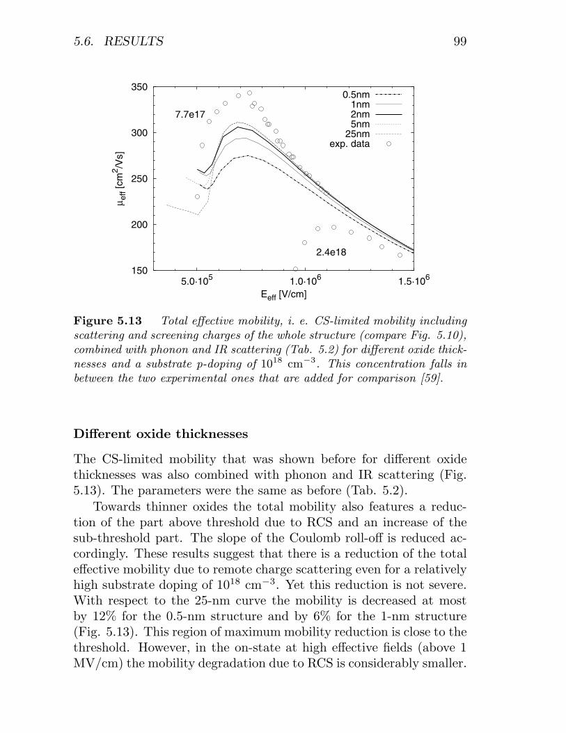
5.6. RESULTS 99
150
200
250
300
350
5.0·105 1.0·106 1.5·106
µ eff
[cm
2 /Vs]
Eeff [V/cm]
2.4e18
7.7e17
0.5nm1nm2nm5nm
25nmexp. data
Figure 5.13 Total effective mobility, i. e. CS-limited mobility includingscattering and screening charges of the whole structure (compare Fig. 5.10),combined with phonon and IR scattering (Tab. 5.2) for different oxide thick-nesses and a substrate p-doping of 1018 cm−3. This concentration falls inbetween the two experimental ones that are added for comparison [59].
Different oxide thicknesses
The CS-limited mobility that was shown before for different oxidethicknesses was also combined with phonon and IR scattering (Fig.5.13). The parameters were the same as before (Tab. 5.2).
Towards thinner oxides the total mobility also features a reduc-tion of the part above threshold due to RCS and an increase of thesub-threshold part. The slope of the Coulomb roll-off is reduced ac-cordingly. These results suggest that there is a reduction of the totaleffective mobility due to remote charge scattering even for a relativelyhigh substrate doping of 1018 cm−3. Yet this reduction is not severe.With respect to the 25-nm curve the mobility is decreased at mostby 12% for the 0.5-nm structure and by 6% for the 1-nm structure(Fig. 5.13). This region of maximum mobility reduction is close to thethreshold. However, in the on-state at high effective fields (above 1MV/cm) the mobility degradation due to RCS is considerably smaller.

100 CHAPTER 5. QUANTUM-MECHANICAL MOBILITY
5.6.6 Test of simplifications
In addition to the remote screening by quantum mechanical eigen-states in the gate, a much simpler way for including the RCS effectwas studied as well. In this “naive” approach the ionized impuritieswere screened by the unperturbed majority carriers, i.e. the distri-bution of scattering centers was determined by the depletion chargein the gate. No further screening due to a first order perturbation ofthe mobile charge in the gate was included (yet, the screening by thechannel inversion layer was treated as usual).
The resulting mobility is generally lower if compared to the fullquantum-mechanical modeling of screening (Fig. 5.14). The curvesexhibit a stronger Coulomb roll-off towards a considerably lower sub-threshold level. Obviously this “naive” treatment underestimates thescreening effect by the mobile electrons in the gate.
As mentioned in section 5.3.1 some approximations can be applied
102
103
104
105
106
107
106
µ eff
[cm
2 /Vs]
Eeff [V/cm]
1nm2nm5nm
Figure 5.14 Results (filled symbols) for the “naive” modeling of theRCS-limited effective mobility compared to the full quantum-mechanicaltreatment (empty symbols) which are taken from Fig. 5.8.
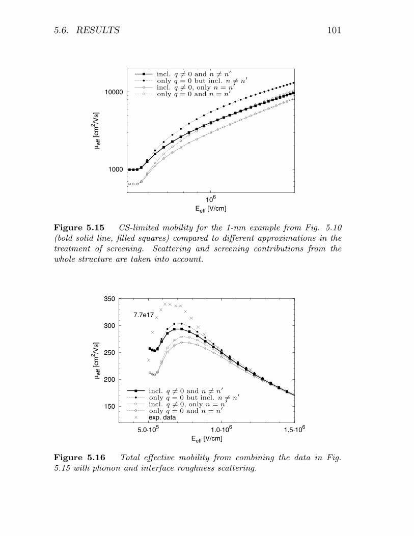
5.6. RESULTS 101
1000
10000
106
µ eff
[cm
2 /Vs]
Eeff [V/cm]
incl. q = 0 and n = n′only q = 0 but incl. n = n′incl. q = 0, only n = n′only q = 0 and n = n′
Figure 5.15 CS-limited mobility for the 1-nm example from Fig. 5.10(bold solid line, filled squares) compared to different approximations in thetreatment of screening. Scattering and screening contributions from thewhole structure are taken into account.
150
200
250
300
350
5.0·105 1.0·106 1.5·106
µ eff
[cm
2 /Vs]
Eeff [V/cm]
7.7e17
exp. data
incl. q = 0 and n = n′only q = 0 but incl. n = n′incl. q = 0, only n = n′only q = 0 and n = n′
Figure 5.16 Total effective mobility from combining the data in Fig.5.15 with phonon and interface roughness scattering.

102 CHAPTER 5. QUANTUM-MECHANICAL MOBILITY
to the induced screening charge. Their effects on the CS-limited mo-bility are compared in Fig. 5.15 for the 1-nm structure. Scattering andscreening from either side of the oxide have been taken into account.In the long-wavelength limit, i.e. using L(q = 0) for the polarizationfactor, the screening is stronger because the decay of L(q) for q → ∞is neglected. Consequently, the mobility is higher. Below inversion,however, the same sub-threshold mobility is obtained. If the inter-subband contributions (n = n′) are ignored screening is weaker overthe whole range of effective fields. Using both simplifications leads toan overestimation of the Coulomb roll-off. The close agreement withthe full treatment at high fields is probably a coincidence.
These approximations also have some influence on the total mo-bility which is again shown for the 1-nm structure (Fig. 5.16).
5.6.7 Comparison to literature data
Publications of experimental mobility data for ultra-thin oxides arenot abundant but there are a few [61,85–87]. They report a loweringof the measured effective mobility associated with thin gate oxides inpolysilicon-gated MOSFETs. It has to be noted that each researchgroup has developed their own method to deal with the problem ofmobility extraction in the presence of gate leakage.
Takagi and Takayanagi examine oxide thicknesses down to 1.5 nmfor a substrate doping of 3 · 1016 cm−3 [61]. Using Mathiessen’s rulethey extract the additional mobility contribution that produces thelowering but which is almost independent of the inversion layer sheetdensity. They conclude that this behavior can not be explained byRCS or other mechanisms like remote plasmon or remote interfaceroughness scattering. In subsequent publications, Koga et al. usevery lowly doped substrates in order to exclude substrate impurityscattering [62, 85]. They find that RCS and an enhanced IR mayexplain their results. The latter is ascribed to a possibly poorer qualityof the Si/SiO2 interface for the thin-oxide samples.
Lucci et al. compare experimental and simulated effective mobil-ity for oxide thicknesses down to 1.15 nm and a substrate doping of3 · 1015 cm−3 [87]. They conclude that the effect of RCS can quantita-tively explain the mobility reduction but should be hardly detectablefor higher substrate dopings.

5.6. RESULTS 103
5×10⁵
1×10⁶
2×10⁶
Eeff [V/cm]
100
150
200
250
300
350
µ eff [
cm2 /V
s]
5nm2nm1nmLime et al. ’03
1.2 nm
2.5 nm
Figure 5.17 Total effective mobility curves from 5.13 for tox = 1, 2 and5 nm (lines) compared to measurements of Ref. [86] (tox =1.2 to 2.5 nm,filled symbols)
Lime et al. present mobility measurements for a higher substratedoping (8−9 ·1017 cm−3) which is close to the one examined here [86].They introduce a correction to the calculation of the inversion layercharge Qinv as a function of the gate voltage VGS in order to eliminatea difference between the threshold voltage of Qinv(VGS) and the oneof the transfer characteristics. As it is not expected that similar ma-nipulations have been used elsewhere, we chose to compare with theiruncorrected data: The mobility curves (for tox =1.2, 1.5, 1.8 and 2.5nm) exhibit a much stronger separation with oxide thickness than oursimulation results (Fig. 5.17). Furthermore, the experimental mobili-ties are considerably smaller although the gate impurity concentrationis lower (5 · 1019 cm−3). This may indicate that RCS alone is not suf-ficient to explain the lowering but that other, additional scatteringmechanisms appear to contribute with decreasing oxide thickness. Itshould also be mentioned that they use a different value for η in thecalculation of the effective field (η = 0.6− 0.7).
RCS is also included in Monte Carlo simulations by Gamiz et al.
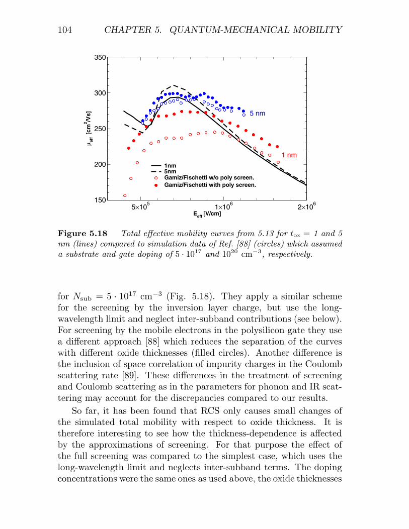
104 CHAPTER 5. QUANTUM-MECHANICAL MOBILITY
5×10⁵
1×10⁶
2×10⁶
Eeff [V/cm]
150
200
250
300
350
µ eff [
cm2 /V
s]
1nm5nmGamiz/Fischetti w/o poly screen.Gamiz/Fischetti with poly screen.
1 nm
5 nm
Figure 5.18 Total effective mobility curves from 5.13 for tox = 1 and 5nm (lines) compared to simulation data of Ref. [88] (circles) which assumeda substrate and gate doping of 5 · 1017 and 1020 cm−3, respectively.
for Nsub = 5 · 1017 cm−3 (Fig. 5.18). They apply a similar schemefor the screening by the inversion layer charge, but use the long-wavelength limit and neglect inter-subband contributions (see below).For screening by the mobile electrons in the polysilicon gate they usea different approach [88] which reduces the separation of the curveswith different oxide thicknesses (filled circles). Another difference isthe inclusion of space correlation of impurity charges in the Coulombscattering rate [89]. These differences in the treatment of screeningand Coulomb scattering as in the parameters for phonon and IR scat-tering may account for the discrepancies compared to our results.
So far, it has been found that RCS only causes small changes ofthe simulated total mobility with respect to oxide thickness. It istherefore interesting to see how the thickness-dependence is affectedby the approximations of screening. For that purpose the effect ofthe full screening was compared to the simplest case, which uses thelong-wavelength limit and neglects inter-subband terms. The dopingconcentrations were the same ones as used above, the oxide thicknesses

5.6. RESULTS 105
5×10⁵
1×10⁶
2×10⁶
Eeff [ V/cm ]
150
200
250
300
350
µ eff [
cm
2 Vs
]
5 nm
1 nm
2.5 nm1.2 nm
Figure 5.19 Total effective mobility for two oxide thicknesses tox = 1and 5 nm using the full screening (solid symbols, solid lines) compared to thelong-wavelength limit without inter-subband terms (empty symbols, dashedlines) and the experimental data of Lime et al. [86] (dotted lines).
were tox = 1 and 5 nm. It was found that the simpler treatment resultsin a stronger dependence on oxide thickness of the total mobility (Fig.5.19). In addition, the separation increases by a factor of two and themobility falls to lower values at low effective fields, i.e. the Coulombroll-off appears to be more pronounced.
In addition, simulations for a substrate doping of 3 · 1016 cm−3
and a gate doping of 5 · 1019 cm−3 using the full and the simplifiedscreening were compared to the aforementioned data of Takagi andTakayanagi (Fig. 5.20). Again the full inclusion of screening pro-duces only a weak dependence on oxide thickness (solid lines). Usingthe long-wavelength limit and omitting inter-subband contributionsroughly doubles the separation between the curves (dashed lines) andthe overall reduction of the mobility is more pronounced. It is strikingthat the experimental roll-off at low fields is much stronger than thesimulated one. As seen before, the simulated curves fail to reproducethe actual Eeff-dependence of the universal behavior in the range oflower effective fields.
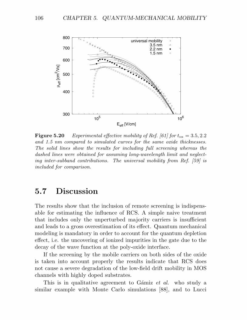
106 CHAPTER 5. QUANTUM-MECHANICAL MOBILITY
300
400
500
600
700
800
105 106
µ eff
[cm
2 /Vs]
Eeff [V/cm]
universal mobility3.5 nm2.2 nm1.5 nm
Figure 5.20 Experimental effective mobility of Ref. [61] for tox = 3.5, 2.2and 1.5 nm compared to simulated curves for the same oxide thicknesses.The solid lines show the results for including full screening whereas thedashed lines were obtained for assuming long-wavelength limit and neglect-ing inter-subband contributions. The universal mobility from Ref. [59] isincluded for comparison.
5.7 Discussion
The results show that the inclusion of remote screening is indispens-able for estimating the influence of RCS. A simple naive treatmentthat includes only the unperturbed majority carriers is insufficientand leads to a gross overestimation of its effect. Quantum mechanicalmodeling is mandatory in order to account for the quantum depletioneffect, i.e. the uncovering of ionized impurities in the gate due to thedecay of the wave function at the poly-oxide interface.
If the screening by the mobile carriers on both sides of the oxideis taken into account properly the results indicate that RCS doesnot cause a severe degradation of the low-field drift mobility in MOSchannels with highly doped substrates.
This is in qualitative agreement to Gamiz et al. who study asimilar example with Monte Carlo simulations [88], and to Lucci
5.7. DISCUSSION 107
et al. who find only modest mobility lowering also for lower doping(3 · 1015 cm−3) in both measurements and simulation [87]. Both worksalso include polysilicon screening in their models. However, they usethe long-wavelength limit and neglect the inter-subband contributionsto screening. One of them, [88], also applies a different approach forthe gate region.
In comparison to experimental results of Lime et. al. the simu-lated mobility is clearly to high. The same seems to apply for thedata of Takagi/Takayanagi although it may be masked by possibleshortcomings of the phonon model in the respective range of effectivefields. The reasons for these differences are unclear. One might thinkof other scattering mechanisms that are associated with thin oxides inthe literature: Fischetti theoretically examines remote plasmon scat-tering, i.e. long-range Coulomb-interactions of the electrons in thechannel with the ones in the gate [90]. This is also called “gate drag”,as momentum is transferred to the mobile charge in the gate whichcauses a mobility degradation in the channel. However, it remains atopic to be further examined as neither from theory (at least at lowinversion densities [90]) nor from experiment [91] the importance ofthis effect has been established, yet.
Another candidate would be remote interface roughness [92, 93],i.e. the influence of the irregularities in the oxide-polysilicon interface,which is generally less ideal compared to the one on the channel side.
Apart from additional scattering it is also possible that the screen-ing effect is overestimated. One should note that the reported goodagreements between experimental and modeled effective mobilities forthin gate oxides [87,88] were obtained with a simpler model for screen-ing than the one used here. This simplification, however, appears toreduce screening which – regarding the mobility degradation in theexperiments – provides a shift into the desired direction. Regardingtheory, however, this might be a hint that using only first order cor-rections is not sufficient. For example, correlation effects among themobile carriers are neglected but they might reduce their ability toscreen the Coulomb interaction with ionized impurities.
In addition, it has been found that – below threshold – remotescreening from the mobile carriers in the gate even affects the im-purity scattering in the channel (while RCS is switched off). Thesub-threshold mobility is lifted, the more for thinner oxides, although

108 CHAPTER 5. QUANTUM-MECHANICAL MOBILITY
the interacting particles (electrons and ionized acceptors) are locatedon the other side.
By the Fourier transformation of the Poisson equation it was im-plicitly assumed that the structure extends to infinity in the in-planecoordinates. Of course this is not valid in a real device neither forthe substrate impurities (as sources of scattering) nor for the mobilecharge in the gate (as a screening medium). To study the impact offinite in-plane dimensions is, however, beyond the scope of this work.
Several aspects are left to examine with regard to Coulomb scat-tering and RCS: These are the dependence on temperature, the useof other gate (high-k) dielectrics and the mobility modeling for thinsilicon films in SOI and double gate structures. For the latter a secondsource of remote effects comes into play. To include it, the Green’sfunction needs to be extended by additional regions of different di-electric constant.
For the calculation of a total effective mobility the phonon modelof Ref. [11] was adopted. For IR scattering a pragmatic approachwas chosen by using an unscreened model that allowed the closestreproduction of the universal behavior. Nevertheless, there are stilldiscrepancies at low effective fields. To reduce these, the models forphonon and IR scattering need to be improved.
From a theoretical point of view the screening of IR as done byWettstein appears to be correct as it self-consistently includes firstorder corrections [11]. The IR screening presented here is a refor-mulation which, however, neglects the perturbations of the dielectricconstant (it should also be noted that Wettstein only includes thelowest subbands in each valley). That screening has to be neglectedfor fitting to experimental results shows that the modeling of IR isstill poorly understood. As for Coulomb scattering one might suspectthat the screening effects are too strong in the hitherto used modelingattempts.
One should also be aware of the approximations done in IR scat-tering. It is possible that first order perturbation theory may not beaccurate enough for this mechanism. In addition, the matrix elementshave been linearized in the interface shift ∆(x‖) to enable a simplemultiplication with the roughness spectrum. This is convenient buthigher order terms are neglected.
Another topic to examine further regarding IR is the form of the

5.7. DISCUSSION 109
power spectrum. There have been investigations in order to modelelectron and hole mobilities using an identical expression for bothcarrier species [83, 94].
Already for a perfectly flat interface the amorphous structure ofthe oxide should give rise to scattering because a tail of the elec-tronic wave function penetrates the oxide and experiences a spatialinhomogeneity along its traveling direction. This is not IR scatteringanymore, but it is related as it is due to the presence of an interfacewith a disordered material behind it. To model this effect Polishchukand Hu include a simple E2
eff -dependent mobility with a single fitparameter via Matthiessen’s rule [95]. An interesting aspect of thisscattering mechanism is that it should be unaffected by screening.


Appendices
Appendix A:Local density of states
In this section, the concept of a local density of states is illustratedby a few examples. First of all the local DOS is in general defined as
N(E, r) = 2∑j
|Ψj(r)|2δ(E −Ej) , (A.1)
with the envelope wave function Ψj corresponding to the eigenenergyEj and j being a set of quantum numbers characterizing the eigen-states. A factor of 2 is included for the spin.
A.1 Bulk case with almost constant potential
For the bulk semiconductor the usual assumption is made that thewave functions can be represented by plane waves Ψk(r) = exp(ik ·r)/
√V (where V = LxLyLz is the normalization volume). The quan-
tum numbers j are then given by the wave vector k. The summationtransforms into V/(2π)3
∫d3k and the usual DOS expression is ob-
tained:N(E) =
2(2π)3
∫d3k δ(E − Ek) , (A.2)
which yields the well-known square-root DOS for parabolic bands(Ek = Ec + (k2
x/mx + k2y/my + k2
z/mz)2/2):
N(E) =1
2π2
(2m∗
2
)3/2√E−Ec Θ(E−Ec) , (A.3)
111

112 CHAPTER 5. QUANTUM-MECHANICAL MOBILITY
This is strictly valid only for constant potential. However, a spatialdependency is often re-introduced via the band edge Ec(r).
A.2 Local DOS in an electric field
In contrast to the plane wave approximation, now the influence ofthe potential on the form of the wave functions shall be taken intoaccount. The potential is assumed to be non-constant only alongthe z-direction with one classical turning point. The motion in thez-direction is then described by the eigenenergy E⊥ and the wavefunction ψ(E⊥, z) which leads to the following ansatz for the totalwave function:
Ψκ,E⊥(r) = (LxLy)−1/2 exp(iκ · x‖) ψ(E⊥, z) , (A.4)
and the total energy
E(κ, E⊥) = E⊥ +
2κ2
2mxy, (A.5)
where again parabolic bands have been assumed. The wave andposition vectors perpendicular to the z-direction are κ and x‖, re-spectively. After integrating over E⊥, the local DOS retains a z-dependence:
N(E, z) =1
2π2
∫d2κ
∣∣∣∣ψ(E − 2κ2
2mxy, z
)∣∣∣∣2 . (A.6)
In the special case of a homogeneous field F the one-dimensionalSchrodinger equation has the solution [96]
ψ(E, z) =√
2mz
2qzAi (qz(z − zE )) , (A.7)
qz = (2mze F/2)1/3 , (A.8)
where Ai(x) := 1/π∫∞
0cos
(t3/3 + tx
)dt is the Airy function [97] and
zE = E/(eF ) denotes the classical turning point. With this expres-sion, the integration in (A.6) produces
Nc(E, z) =(2m∗
2
)3/2 √θz2π
F(
eFz −E
θz
), (A.9)

5.7. DISCUSSION 113
with θz = (e2F 2/(2mz))1/3 and the electro-optical function [45,98]
F(x) :=∫ ∞
x
dξAi2(ξ) = (Ai′(x))2 − xAi(x)2 . (A.10)
For vanishing field F expression (A.9) approaches the bulk DOS (A.3)which can be seen from the limit:
√aF(x/a) −−−→
a→0
√−xΘ(−x).
A.3 Local DOS for bound states
In the case of bound states, the integral over E⊥ is replaced by a sum∑i over discrete eigenstates ψi and eigenenergies Ei:
Nc(E, z) =∑i
2(2π)2
∫d2κ|ψi(z)|2δ
(E − Ei −
2κ2
mxy
)=
mxy
π2
∑i
|ψi(z)|2Θ(E −Ei) . (A.11)
A reasonable approximation for an NMOS inversion layer is thetriangular potential: For z ≤ 0 the potential is infinite, i.e. the elec-tron is only allowed to reside in the region z > 0 where the potentialis Fz. Solutions are those Airy functions that vanish at z = 0. Withproper normalization, these are
ψi(z) =√
qzF(−qzzi)
Ai(qz(z − zi)) , (A.12)
where qz is the same as above and zi = Ei/(eF ) is the right classi-cal turning point for the ith eigenstate. The eigenenergies are Ei =−eFai/qz, where the ai are the zeros of the Airy function. An ap-proximation for the eigenenergies is obtained from the asymptoticexpansion of the zeros [77, 97, 99]:
Ei ≈ eF
qz
(3π2
(i +
34
))2/3
, for i = 0, 1, 2, . . . (A.13)
This formula improves with increasing i. For i = 0 the error is alreadybelow 1%, for i = 2 below 0.1%. More accurate values are listed intable A.1. With these solutions the local DOS (A.11) approachesexpression (A.9) for large distances z from the barrier (see Fig. A.1).

114 CHAPTER 5. QUANTUM-MECHANICAL MOBILITY
i −ai0 2.33810741 4.08794942 5.52055973 6.78670814 7.94413365 9.0226509
Table A.1 Numerical values for the first zeros ai of the Airy function[97].
0
1
2
3
4
5
6
7
8
9
10
-0.2 -0.1 0 0.1 0.2 0.3 0.4 0.5
DO
S [
1020
/cm
3 /eV
]
QCDOS at z=50nm
QCDOS at z=5nm
FKDOS
bulk DOS
E − Ec(z) [eV]
Figure A.1 Local DOS of bound states (QCDOS) in a triangular well atdifferent distances from the wall for a field of F=106 V/cm. For comparison,the bulk DOS and FKDOS are also shown. Only one silicon valley withmz = ml and mxy = mt was considered.

5.7. DISCUSSION 115
Appendix B:Green’s function
Eq. (5.23) is the Fourier transform of
∇ · (ε∇V (r)) = −ρ(r) , (B.1)
where r = (x‖, z) and it is assumed that the dielectric constant ε doesnot depend on x‖ and is piecewise constant in z.
For the moment, a bulk material is assumed, i.e. that ε is a con-stant also in z. Then, for a point like charge placed at r0 = (x0, z0)the solution for any ρ is given by
V (r) =∫
d3r0 GC(r, r0)ρ(r0) , (B.2)
with a Green’s function which is the Coulomb potential
GC(r, r0) = GC(x‖, z,x0, z0) =1
4πε√|x‖ − x0|2 + (z − z0)2
. (B.3)
The Fourier transforms of GC and V with respect to x‖ are
GC(q, z,x0, z0) = G(q, z, z0) exp(−iq · x0) (B.4)
and
V (q, z) =∫
dz0 G(q, z, z0)ρ(q, z0) , (B.5)
respectively, where G is the solution of
(∂zε ∂z − q2ε)G(q, z, z0) = −δ(z − z0) . (B.6)
For constant ε this is
G(q, z, z0) = Gbulk(q, z, z0) :=1
2 ε qexp(−q|z − z0|) . (B.7)
The equations (B.4–B.6) still hold if one goes back to layers of ma-terials with different dielectric constants ε. Inside each layer, Gbulk,
116 CHAPTER 5. QUANTUM-MECHANICAL MOBILITY
with ε = ε(z), and V are still particular solutions of (B.6) and (B.1),respectively. But in the end V and ε∂V∂z must fulfill continuity condi-tions at the interfaces. This requires the addition of an appropriatehomogeneous solution (AX exp(−qz) +BX exp(qz) in each region X)to either V or Gbulk. Here, the latter is chosen.
First a single interface located at z = 0 between two materials withdielectric constants εA,B is considered (see Fig. B.1). The Green’sfunction in material X for a point charge in material Y is denoted byGXY (q, z, z0, εL , εR), where εL and εR are the dielectric constants ap-plied for z < 0 and z > 0, respectively. All four possible combinationsare listed here [yet, two of the functions (e. g. GAA and GAB) wouldsuffice]:
GAA(q, z, z0, εA , εB) =
12 q εA
(e−q|z−z0| +
εA−εBεA+εB
eq(z+z0)
)(B.8)
GAB(q, z, z0, εA , εB) =12 q
2εA+ε
B
eq(z−z0) (B.9)
GBA(q, z, z0, εA , εB) =12 q
2εA+εB
eq(z0−z)
= GAB(q,−z,−z0, εB , εA)(B.10)
GBB(q, z, z0, εA , εB) =1
2 q εB
(e−q|z−z0| +
εB−εAεA+ε
B
e−q(z+z0)
)= GAA(q,−z,−z0, εB , εA) .
(B.11)
For two interfaces located at z = −d and z = 0 separating threematerials (see Fig. B.2), the notation is analog. There are nine com-
0
A B
z
Figure B.1 Two materials.

5.7. DISCUSSION 117
binations for the source and probe location, i. e. z0 and z:
GAB(q, z, z0, εA , εB, ε
C) =
12q
2C
εB+εA
(e−q(z−z0) + kc eq(z+z0)
)(B.12)
GAC(q, z, z0, εA , εB , εC ) =12q
4C εBe−q(z−z0)
(εB+ε
A)(ε
B+ε
C)
(B.13)
GBB(q, z, z0, εA , εB, ε
C) =
12q
1εB
(e−q|z−z0|+
+ C[kae−q(z+z0+2d) + kceq(z+z0)+
+ kakc
(eq(z−z0−2d) + e−q(z−z0+2d)
) ]) (B.14)
GBC(q, z, z0, εA , εB , εC ) =2C
(kae−q(z+z0+2d) + e−q(z−z0)
)2q(ε
B+ε
C)
(B.15)
GCC(q, z, z0, εA , εB , εC ) =12q
1εC
(e−q|z−z0|+
+ C(kae−q(z+z0+2d) − kce−q(z+z0)
)) (B.16)
GAA(q, z, z0, εA , εB, ε
C) = GCC(q,−z−d,−z0−d, ε
C, ε
B, ε
A) (B.17)
GBA(q, z, z0, εA , εB , εC ) = GBC(q,−z−d,−z0−d, εC , εB , εA) (B.18)GCA(q, z, z0, εA , εB , εC ) = GAC(q,−z−d,−z0−d, εC , εB , εA) (B.19)GCB(q, z, z0, εA , εB , εC ) = GAB(q,−z−d,−z0−d, εC , εB , εA) , (B.20)
0
A B C
z−d
Figure B.2 Three materials.

118 CHAPTER 5. QUANTUM-MECHANICAL MOBILITY
where
ka =εB− ε
A
εB + εA, (B.21)
kc =εB − εCεB + εC
, (B.22)
C =1
1− kakc exp(−2dq). (B.23)

5.7. DISCUSSION 119
Appendix C:Polarization factor
With the assumption of a linear reaction of the density, first orderperturbation theory yields the following general expression for thepolarization factor (including dynamic effects, the factor of 2 accountsfor the spin degeneracy):
Lnn′
νν′(q, ω, T, µ) =
2LxLy
∑κ
fnν(κ)− fn′ν′(κ + q)Enν(κ)− En′ν′(κ + q) + ω + iα
(C.1)
=1
2π2
∫d2κ
fnν(κ)− fn′ν′(κ + q)Enν(κ)−En′ν′(κ + q) + ω + iα
, (C.2)
where ω is the angular frequency of an oscillatory perturbation pro-portional to exp(−iωt) and α is an infinitesimal positive number thatensures that the perturbation vanishes at times t → −∞.
From now on it is assumed that both states n and n′ belong tothe same valley, therefore the valley index is dropped for the sake ofsimplicity.
If fn(κ) can be replaced by the Fermi distribution the polar-ization factor can be obtained from its zero-temperature expressionL(q, ω, T = 0, µ) by the following integral [100]:
Lnn′(q, ω, T, µ) =
∫ ∞
−∞dµ′ Ln
n′(q, ω, T=0, µ′)
cosh2(µ−µ′2kT
) , (C.3)
where µ is the Fermi energy.For T = 0 the Fermi distribution is a step function in energy:
Lnn′(q, ω, T=0, µ) =
12π2
∫d2κ
Θ(µ−En(κ))−Θ(µ−En′(κ + q))En(κ)− En′(κ + q) + ω + iα
.
(C.4)In the following a parabolic band structure is assumed. The integralis split into a sum of two and in the second one κ + q is substitutedby κ. Then, in both integrals κ is substituted according to:
κ =(κxκy
)=(√
mx/m0 00
√my/m0
)κ , (C.5)

120 CHAPTER 5. QUANTUM-MECHANICAL MOBILITY
where m0 is some reference mass. Similarly q is replaced by q. With-out the restriction to stay within one valley these transformationscould not have been done. One obtains:
Lnn′ = −
√mxmy
2π2 2 q
∫ ∞
0
dκ
∫ 2π
0
dϕΘ(µ−En −
2κ2
2m0
)cosϕ− q
2κ (γnn′(q, ω)− 1)− iα+
∫ 2π
0
dϕΘ(µ−En′ −
2κ2
2m0
)cosϕ− q
2κ (γnn′(q, ω) + 1)− iα
(C.6)
with
γnn′(q, ω) =ω + En − En′
Eq and Eq =
2q2
2√mxmy. (C.7)
The two integrals over the azimuth angle ϕ have the same form andgive the following result in the limit of vanishing positive y [65]:∫ 2π
0
dϕ1
cosϕ− x− iy=
−2π√x2 − 1
(Θ(x + 1)−Θ(−x− 1)) . (C.8)
After some algebra one finds:
Lnn′(q, ω, T = 0, µ) = −
√mxmy
2π2×[
Θ(µ−En)1−γnn′ + sign(βn+γnn′−1)
√(γnn′−1)2−β2
n
+
Θ(µ−En′)1+γnn′−sign(βn′+γnn′+1)
√(γnn′+1)2−β2
n′
](C.9)
whereβn(q) = 2
√(µ−En)/Eq . (C.10)
It should be noted that in the static case (ω = 0) the two roots actuallyhave identical arguments:
(γnn′ − 1)2 − β2n =
4(µ− µ)Eq = (γnn′ + 1)2 − β2
n′ (C.11)

5.7. DISCUSSION 121
with:
µ :=(En −En′)2 + 2Eq(En + En′) + E2
q
4Eq . (C.12)
A non-zero imaginary part therefore only exists if µ > µ and if thetwo sign functions differ. Their arguments are not equal but as afunction of µ they change sign simultaneously at µ = µ, both fromnegative to positive sign. Hence, the imaginary part is always zero sothat in the static case the polarization factor is always a real quantity,in contradiction to the statement in [65].
A different way to calculate the static polarization factor is de-scribed by Wettstein [11]. It is based on time-independent perturba-tion theory and does not need the T = 0 limit. It is also restrictedto the intra-valley case and parabolic band structure. Starting from(C.2) with ω = α = 0 he obtained:
Lnn′(q, ω = 0, T, µ) = −
√mxmy
π2×∫ 1
0
dλ f0
(λEn′ + (1− λ)En − λ(λ− 1)
2
2
(q2x
mx+
q2y
my
)) (C.13)
where f0(E) = (1 + exp((E − µ)/kT ))−1 is the Fermi distribution.1
The long wavelength limit: q → 0
In the long wavelength limit, i. e. for small scattering wave vector q,Eq. (C.4) becomes:
Lnn′(q=0,ω, T=0, µ) =
√mxmy
π2×
× (µ−En)Θ(µ−En)− (µ−En′)Θ(µ−En′)En −En′ + ω + iα
.
(C.14)
For finite temperatures Eq. (C.3) yields:
Lnn′(q=0, ω, T, µ) =
√mxmy
π2
kT ln(f0(En′ )f0(En)
)−En + En′
En −En′ + ω + iα. (C.15)
1For this formula to be valid the function f0 is not necessarily restricted tobeing the Fermi distribution, but it has to be differentiable in E.
122 CHAPTER 5. QUANTUM-MECHANICAL MOBILITY
In the static case that is used here the expression reduces to
Lnn′(q=0, ω=0, T, µ) =
√mxmy
π2
kT ln(f0(En′ )f0(En)
)En −En′
− 1
(C.16)
and simplifies further for the intra-subband polarization factor (n′ =n) [101]:
Lnn(q=0, ω=0, T, µ) = −
√mxmy
π2f0(En) . (C.17)

Bibliography
[1] G. E. Moore. Cramming more components onto integrated cir-cuits. Electronics, 38(8), 1965.
[2] International Technology Roadmap for Semiconductors, 2004Update. Published online at http://public.itrs.net.
[3] J. Bardeen. Tunnelling from a many-partice point of view. Phys.Rev., 6:57–59, 1961.
[4] W. A. Harrison. Tunnelling from an independent-particle pointof view. Phys. Rev., 6:85–89, 1961.
[5] A. Schenk and G. Heiser. Modeling and simulation of tunnelingthrough ultra-thin gate dielectrics. J. Appl. Phys., 81:7900–7908, 1997.
[6] F. Stern and W. E. Howard. Properties of semiconductor sur-face inversion layer in the electric quantum limit. Phys. Rev.,163(3):816–835, 1967.
[7] W. Brauer and H. W. Streitwolf. Theoretische Grundlagen derHalbleiterphysik. Akademie Verlag, Berlin, 1977.
[8] R. Enderlein and N. J. M. Horing. Fundamentals of Semicon-ductor Physics and Devices. World-Scientific, Singapore, NewJersey, London, Hong Kong, 1996.
[9] R. Enderlein and A. Schenk. Grundlagen der Halbleiterphysik.Akademie Verlag, Berlin, 1992.
123

124 BIBLIOGRAPHY
[10] D. J. BenDaniel and C. B. Duke. Space-Charge Effects on Elec-tron Tunneling. Phys. Rev., 152(2):683–692, 1966.
[11] A. Wettstein. Quantum Effects in MOS Devices. Hartung–GorreVerlag, Konstanz, 2000.
[12] L. Dekar, L. Chetouani, and T. F. Hammann. Wave function forsmooth potential and mass step. Phys. Rev. A, 59(1):107–112,1999.
[13] F. O. Heinz. Simulation Approaches for Nanoscale Semiconduc-tor Devices. Hartung–Gorre Verlag, Konstanz, 2004.
[14] C. Jacoboni, R. Minder, and G. Majni. Effects of band non-parabolicity on electron drift velocity in silicon above room tem-perature. J. Phys. Chem. Solids, 36:1129–1133, 1975.
[15] ISE AG. ISE TCAD Manuals, Release 10.0, DESSIS. Zurich,2004.
[16] A. Schenk. Advanced Physical Models for Silicon Device Simu-lation. Springer-Verlag, Wien, New York, 1998.
[17] A. Schenk. Halbleiterbauelemente – Physikalische Grundlagenund Simulation, 2001. Lecture notes:http://www.iis.ee.ethz.ch/~schenk/lecture.html.
[18] K. Bløtekjær. Transport Equations for Electrons in Two-ValleySemiconductors. IEEE Trans. Electron Devices, 17(1):38–47,1970.
[19] E. Schrodinger. Quantisierung als Eigenwertproblem. Ann.Phys., 79:361–376, 1926.
[20] E. Madelung. Quantentheorie in hydrodynamischer Form.Z. Phys., 40:322–327, 1926.
[21] M. G. Ancona and H. F. Tiersten. Macroscopic physics of thesilicon inversion layer. Phys. Rev. B, 35:7959–7965, 1987.
[22] E. Wigner. On the quantum correction for thermodynamic equi-librium. Phys. Rev., 40:749–759, 1932.

BIBLIOGRAPHY 125
[23] M. G. Ancona and G. J. Iafrate. Quantum correction to theequation of state of an electron gas in a semiconductor. Phys.Rev. B, 39:9536–9540, 1989.
[24] C. L. Gardner. The Quantum Hydrodynamic Model for Semi-conductor Devices. SIAM J. Appl. Math., 54(2):409–427, 1994.
[25] C. L. Gardner and C. A. Ringhofer. The Smooth QuantumPotential for the Hydrodynamic Model. Phys. Rev. E, 53:157–167, 1996.
[26] A. Wettstein, A. Schenk, and W. Fichtner. Quantum Device-Simulation with the Density-Gradient Model on UnstructuredGrids. IEEE Trans. Electron Devices, 48:279–284, 2001.
[27] A. Wettstein, O. Penzin, and E. Lyumkis. Integration of theDensity Gradient Model into a General Purpose Device Simu-lator. VLSI Design, 15(4):751–759, 2002.
[28] B. Wu and T.-W. Tang. Quantum Corrected Boltzmann Trans-port Model for Tunneling Effects. In Proc. of the SISPAD, pages279–282. IEEE, 2003.
[29] M. G. Ancona. Equation of State for Silicon Inversion Layers.IEEE Trans. Electron Devices, 47(10):1449–1456, 2000.
[30] M. G. Ancona. Macroscopic description of quantum-mechanicaltunneling. Phys. Rev. B, 42:1222–1233, 1990.
[31] M. G. Ancona. Density-Gradient Theory Analysis of Elec-tron Distributions in Heterostructures. Superlatt. and Microstr.,7(2):119–130, 1990.
[32] J. Maserjian and G. P. Petersson. Tunneling through thin MOSstructures: Dependence on energy (E-κ). Appl. Phys. Lett.,25(1):50–52, 1974.
[33] A. Schenk and A. Wettstein. 2D Analysis of Source-to-DrainTunneling in Decananometer MOSFETs with the Density Gra-dient Model. In M. Laudon and B. Romanowicz, editors, Proc.of the 5th Int. Conf. on Modeling and Simulation of Microsys-tems, pages 552–555, San Juan, 2002.

126 BIBLIOGRAPHY
[34] T. Hohr, A. Schenk, A. Wettstein, and W. Fichtner. On Density-Gradient Modeling of Tunneling through Insulators. IEICETrans. Electron., E86-C(3):379–384, 2003.
[35] R. Clerk, A. Spinelli, G. Ghibaudo, and G. Pananakakis. Theoryof direct tunneling current in metal-oxide-semiconductor struc-tures. J. Appl. Phys., 91:1400–1409, 2002.
[36] ISE AG. ISE TCAD Manuals, Release 8.0, DESSIS. Zurich,2002.
[37] A. Schenk. unpublished.
[38] M. G. Ancona, Z. Yu, R. W. Dutton, P. J. Vande Voorde,M. Cao, and D. Vook. Density-Gradient Analysis of MOS Tun-neling. IEEE Trans. Electron Devices, 47:2310–2319, 2000.
[39] R. Pinnau and A. Unterreiter. The Stationary Current-VoltageCharacteristics of the Quantum Drift-Diffusion Model. SIAMJ. Numer. Anal., 37(1):211–245, 1999.
[40] J. Hontschel. Simulation und Optimierung komplexer nanoelek-tronischer Strukturen. Der andere Verlag, Tonning, 2004.
[41] W. Shockley and W. T. Read. Statistics of the Recombinationof Holes and Electrons. Phys. Rev., 87(5):835–842, 1952.
[42] G. G. Zegrya and A. S. Polkovnikov. Mechanisms of Augerrecombination in quantum wells. JETP, 86(4):815–832, 1998.
[43] T. Hohr, A. Schenk, and W. Fichtner. Revised Shockley Read-Hall Lifetimes for Quantum Transport Modeling. J. Appl. Phys.,95(9):4875–4882, 2004.
[44] A. Schenk. An improved approach to the Shockley-Read-Hallrecombination in inhomogeneous fields of space-charge regions.J. Appl. Phys., 71:3339–3349, 1992.
[45] A. Schenk. A Model for the Field and Temperature Dependenceof Shockley-Read-Hall Lifetimes in Silicon. Solid State Elec.,35:1585–1596, 1992.

BIBLIOGRAPHY 127
[46] K. Huang and A. Rhys. Theory of light absorption and non-radiative transitions in F-centres. Proc. Roy. Soc. London, Ser.A, 204(1078):406–423, 1950.
[47] E. Gutsche. Non-Condon Approximations and the Static Ap-proach in the Theory of Non-Radiative Multiphonon Transi-tions. Phys. status solidi B, 109:583–597, 1982.
[48] A. Schenk, D. Suisky, and R. Enderlein. Nonradiative tran-sitions in semiconductors – A general formula for an n-modemodel: The role of promoting and acceping modes. Acta. phys.pol., A71:315–317, 1987.
[49] W. Franz. Einfluss eines Feldes auf eine optische Absorptions-kante. Z. Naturforsch., 13 a:484–489, 1958.
[50] L. V. Keldysh. The Effect of a Strong Electric Field on theOptical Properties of Insulating Crystals. Sov. Phys. JETP,7(5):788–790, 1958.
[51] P. Michler, T. Forner, V. Hofsaß, F. Prins, K. Zieger, F. Scholz,and A. Hangleiter. Nonradiative recombination via strongly lo-calized defects in quantum wells. Phys. Rev. B, 49(23):16632–16636, 1994.
[52] C. Delerue, G. Allan, and M. Lannoo. Theoretical aspects ofthe luminescence of porous silicon. Phys. Rev. B, 48(15):11024–11036, 1993.
[53] S. Jursenas, G. Tamulaitis, G. Kurilcik, and A. Zukauskas. Non-radiative capture of hot photoelectrons by multiphonon emis-sion in highly excited polar semiconductors. Physica Scripta,T79:187–192, 1999.
[54] J. P. Bergman, P O. Holtz, B. Monemar, M. Sundaram, J. L.Merz, and A. C. Gossard. Non-radiative recombination via deeplevel defects in undoped GaAs/AlGaAs quantum wells. Mat.Sci. Forum, 143–147:629–634, 1994.
[55] T. Hori. Gate Dielectrics and MOS ULSIs. Springer-Verlag,Heidelberg, 1997.
128 BIBLIOGRAPHY
[56] J. Koomen. Investigation of the MOST channel conductance inweak inversion. Solid State Elec., 16:801–810, 1973.
[57] C. G. Sodini, T. W. Ekstedt, and J. L. Moll. Charge accumula-tion and mobility in thin dielectric MOS transistors. Solid StateElec., 25(9):833–841, 1982.
[58] A. G. Sabnis and J. T. Clemens. Characterization of the electronmobility in the inverted 〈100〉 Si surface. In Proc. of the IEDM,pages 18–21, Washington D.C., 1979. IEEE, New York.
[59] S. Takagi, A. Toriumi, M. Iwase, and H. Tango. On the uni-versality of inversion layer mobility in Si MOSFET’s: Part I –Effects of substrate impurity concentration. IEEE Trans. Elec-tron Devices, 41(12):2357–2362, 1994.
[60] S. Takagi, A. Toriumi, M. Iwase, and H. Tango. On the uni-versality of inversion layer mobility in Si MOSFET’s: Part II– Effects of surface orientation. IEEE Trans. Electron Devices,41(12):2363–2368, 1994.
[61] S. Takagi and M. Takayanagi. Experimental evidence ofinversion-layer mobility lowering in ultrathin gate oxide melat-oxide-semiconductor field-effect-transistors with direct tunnel-ing current. Jpn. J. Appl. Phys., 41(4B):2348–2352, 2002.
[62] J. Koga, T. Ishihara, and S. Takagi. Quantitative Examinationof Mobility Lowering Associated with Ultrathin Gate Oxidesin Silicon Metal-Oxide-Semiconductor Inversion Layer. Jap. J.Appl. Phys., 43(4B):1699–1703, 2004.
[63] P. Palestri, D. Esseni, and G. Guegan. On the extraction of thechannel current in permeable gate oxide MOSFETs. Solid StateElec., 48:609–615, 2004.
[64] F. M. Bufler. Halbleitertransporttheorie und Monte CarloBauelementsimulation. 2001. Lecture notes:http://www.iis.ee.ethz.ch/stud area/vorlesungen/montecarlo.en.html.
BIBLIOGRAPHY 129
[65] A. Emunds. Dynamische und kinetische Eigenschaften einesquasi 2-dimensionalen Elektronengases. Fotodruck J. MainzGmbH, 1990.
[66] D. Esseni and A. Abramo. Modeling of Electron Mobility Degra-dation by Remote Coulomb Scattering in Ultrathin Oxide MOS-FETs. IEEE Trans. Electron Devices, 50(7):1665–1674, 2003.
[67] S. Mori and T. Ando. Intersubband scattering effects on themobility of a Si (100) inversion layer at lower temperatures.Phys. Rev. B, 19(12):6433–6441, 1979.
[68] W. H. Press, S. A. Teukolsky, W. T. Vetterling, and B. P. Flan-nery. Numerical Recipes in C. Cambridge University Press,Cambridge, 1992.
[69] F. Gamiz, J.A. Lopez-Villanueva, I. Melchor J. A. Jimemenz-Tejada, and A. Palma. A comprehensive model for Coulombscattering in inversion layers. J. Appl. Phys., 75(2):924–934,1994.
[70] F. Gamiz, F. Jimenez-Molinos, J. B. Roldan, and P. Cartujo-Cassinello. Coulomb scattering model for ultrathin silicon-on-insulator inversion layers. Appl. Phys. Lett., 80(20):3835–3837,2002.
[71] K. Yokohama and K. Hess. Monte Carlo study of electronictransport in Al1−xGaxAs/GaAs single-well heterostructures.Phys. Rev. B, 33(8):5595–5606, 1986.
[72] E. D. Siggia and P. C. Kwok. Properties of Electrons in Semicon-ductor Inversion Layers with Many Occupied Electric Subbands.I. Screening and Impurity Scattering. Phys. Rev. B, 2(4):1024–1036, 1970.
[73] T. H. Ning and C. T. Sah. Theory of Scattering Electronsin a Nondegenerate-Semiconductor-Surface Inversion Layer bySurface-Oxide Charges. Phys. Rev. B, 6(12):4605–4613, 1972.
[74] F. Gamiz, J. A. Lopez-Villanueva, J. Banqueri, Y. Ghailan, andJ. E. Carceller. Oxid charge space correlation in inversion layers

130 BIBLIOGRAPHY
II. Three-dimensional oxide charge distribution. Semicond. Sci.Technol., 10:592–600, 1995.
[75] R. E. Prange and T.-W. Nee. Quantum Spectroscopy of theLow-Field Oscillations in the Surface Impedance. Phys. Rev.,168(3):779–786, 1968.
[76] T. Ando. Screening Effect and Quantum Transport in a SiliconInversion Layer in Strong Magnetic Fields. J. Phys. Soc. Jpn.,43(5):1616–1626, 1977.
[77] T. Ando, A. B. Fowler, and F. Stern. Electronic properties oftwo-dimensional systems. Rev. Mod. Phys., 54:437–672, 1982.
[78] Y. Matsumoto and Y. Uemura. Scattering Mechanism and LowTemperature Mobility of MOS Inversion Layers. Jpn. J. Appl.Phys. Suppl., 2(2):367–370, 1974. Proc. 2nd Intern. Conf. onSolid Surfaces, 1974.
[79] S. M. Goodnick, D. K. Ferry, C. W. Wilmsen, Z. Liliental,D. Fathy, and O. L. Krivanek. Surface roughness at the Si(100)-SiO2 interface. Phys. Rev. B, 32(12):8171–8186, 1985.
[80] G. Mazzoni, A. L. Lacaita, L. M. Perron, and A. Pirovano.On Surface Roughness-Limited Mobility in Highly Doped n-MOSFET’s. IEEE Trans. Electron Devices, 46(7):1423–1428,1999.
[81] S. Villa, A. L. Lacaita, L. M. Perron, and R. Bez. Aphysically-based model of the effective mobility in heavily-dopedn-MOSFET’s. IEEE Trans. Electron Devices, 45(1):110–115,1998.
[82] M. V. Fischetti, F. Gamiz, and W. Hansch. On the enhancedelectron mobility in strained-silicon inversion layers. J. Appl.Phys., 92:7320–7324, 2002.
[83] T. Ishihara, K. Matsuzawa, M. Takayanagi, and S. Takagi. Com-prehensive Understanding of Electron and Hole Mobility Lim-ited by Surface Roughness Scattering in Pure Oxides and Oxyni-trides Based on Correlation Function of Surface Roughness. Jap.J. Appl. Phys., 41(4B):2353–2358, 2002.
BIBLIOGRAPHY 131
[84] The MathWorks, Inc. Matlab, versions 6.5 – 7. Internet hom-page: http://www.mathworks.com.
[85] J. Koga, T. Ishihara, and S. Takagi. Effect of Gate Impu-rity Concentration on Inversion-Layer Mobility in MOSFETswith Ultrathin Gate Oxide Layer. IEEE Electron Device Lett.,24(5):354–356, 2003.
[86] F. Lime, C. Guiducci, R. Clerc, G. Ghibaudo, C. Leroux, andT. Ernst. Characterzation of effective mobility by split C(V)technique in N-MOSFETs with ultra-thin gate oxides. SolidState Elec., 47:1147–1153, 2003.
[87] L. Lucci, D. Esseni, J. Loo, Y. Ponomarev, L. Selmi, A. Abramo,and E. Sangiorgi. Quantitative Assessment of Mobility Degrada-tion by Remote Coulomb Scattering in Ultra-Thin Oxide MOS-FETs: Measurements and Simulations. In IEDM Tech. Dig.,pages 463–466, Washington D. C., 2003. IEEE.
[88] F. Gamiz and M. V. Fischetti. Remote-Coulomb scattering inmetal-oxide-semiconductor field effect transistors: Screening byelectrons in the gate. Appl. Phys. Lett., 83(23):4848–4850, 2003.
[89] F. Gamiz, J. B. Roldan, J. E. Carceller, and P. Cartujo. MonteCarlo simulation of remote-Coulomb-scattering-limited mobil-ity in metal-oxide-semiconductor transistors. Appl. Phys. Lett.,82(19):3251–3253, 2003.
[90] M. V. Fischetti. Long-range Coulomb interaction in small de-vices. Part II: Effective mobility in thin-oxide structures. J.Appl. Phys., 89(2):1232–1250, 2001.
[91] P. Solomon and M. Yang. Relevance of Remote Scattering inGate to Channel Mobility of thin-oxide CMOS devices. In IEDMTech. Dig., pages 143–146, San Francisco, 2004. IEEE.
[92] S. Saito, K. Torii, Y. Shimamoto, S. Tsujikawa, H. Hamamura,O. Tonomura, T. Mine, D. Hisamoto, T. Onai, J. Yugami,M. Hiratani, and S. Kimura. Effects of remote-surface-roughness

132 BIBLIOGRAPHY
scattering on carrier mobility in field-effect-transistors with ul-trathin gate dielectrics. Appl. Phys. Lett., 84(8):1395–1397,2004.
[93] F. Gamiz and J. B. Roldan. Scattering of electrons in siliconinversion layers by remote surface roughness. J. Appl. Phys.,94(1):392–399, 2003.
[94] A. Pirovano, A. L. Lacaita, G. Zandler, and R. Oberhuber. Ex-plaining the Dependencies of the Hole and Electron Mobilities inSi Inversion Layers. IEEE Trans. Electron Devices, 47(4):718–724, 2000.
[95] I. Polishchuk and C. Hu. Electron Wavefunction Penetrationinto Gate Dielectric and Interface Scattering – An Alterna-tive to Surface Roughness Scattering Model. In SymposiumOn VLSI Technology Digest of Technical Papers, pages 51–52.IEEE, 2001.
[96] L.D. Landau and E.M. Lifschitz. Lehrbuch der theoretischenPhysik, Quantenmechanik. Akademie Verlag, Berlin, 1985.
[97] M. Abramowitz and I.A. Stegun, editors. Handbook of mathe-matical functions. Dover publications Inc., New York, 1970.
[98] D. E. Aspnes. Electric-Field Effects on Optical Absorption nearThreshold in Solids. Phys. Rev., 147:554–566, 1966.
[99] F. Stern. Self-consistent results for n-type Si inversion layers.Phys. Rev. B, 5:4891–4899, 1972.
[100] P. F. Maldague. Many-body corrections to the polarizability ofthe two-dimensional electron gas. Surf. Sci., 73:296–302, 1978.
[101] D. K. Ferry and S. M. Goodnick. Transport in Nanostructures.University Press, Cambridge, 1997.

Curriculum Vitae
Timm Hohr was born in Celle, Germany, on December 10, 1972. Hestudied physics at the University of Konstanz, Germany, where hereceived his Dipl.-Phys. degree in 2000. In the academic year 1996/97he attended the State University of New York at Stony Brook. In 2001he joined the Integrated Systems Laboratory at ETH Zurich where heworked on numerical modeling of quantization and related transportphenomena in MOS devices.
133