Embed Size (px)
Citation preview
Quantum Interference and Entanglement of
Surface Plasmons
Thesis by
James S. Fakonas
In Partial Fulfillment of the Requirements
for the Degree of
Doctor of Philosophy
California Institute of Technology
Pasadena, California
2015
(Defended November 2014)

ii
c© 2014
James S. Fakonas
All Rights Reserved

iii
To my very patient wife.
iv
Acknowledgements
It has been an honor and a pleasure to work with so many brilliant and creative
people during my time at Caltech. While I can’t possibly acknowledge them all in
this brief note, let alone describe the myriad ways in which they helped me over the
years, I must at least express my gratitude to some of them here and hope that the
others will forgive me for not mentioning them explicitly.
First things first, I am extremely grateful to my adviser, Prof. Harry Atwater.
Harry is an exceptional scientist—this much he is already widely known for—but
even more than that, he is a fantastic mentor. I deeply appreciate Harry’s guidance,
advice, and endless enthusiasm, and I’m especially grateful that he gave me substan-
tial freedom to explore areas of physics that were new to me as the direction of my
thesis research began to take shape. It truly has been a privilege to discuss physics
with somebody so sharp, to brainstorm experiments with somebody so creative, to
share a casual conversation with somebody so genuine, and to work for somebody so
dedicated to the professional development of his students. I wish him absolutely all
the best in his future work.
I would also like to thank Profs. Andrei Faraon, Brent Fultz, Bill Johnson, and
Keith Schwab for serving on my thesis and candidacy committees. Whenever I see
one of them give a technical presentation or ask questions of a visiting scientist, I am
always amazed at the depth and breadth of their scientific knowledge. It is an honor
(but also more than a little intimidating!) to submit this thesis for their examination.
During my time in the Atwater group, I’ve had the opportunity to work with
and learn from a great many bright, dedicated, and ingenious graduate students and
postdocs. I’m especially grateful to Dr. Ryan Briggs, first and foremost, for all of
v
his help over the years. Ryan trained me on the various fabrication equipment in
the KNI, brainstormed ideas for my thesis research with me, helped me troubleshoot
fabrication problems, encouraged me when I struggled, celebrated with me when I
succeeded, and overall set an excellent example of how to be a successful grad stu-
dent. More than all this, though, Ryan has also been a great friend, and I’m lucky
that I’ve had the privilege to know him. I’d also like to thank Dr. Dennis Callahan
for his friendship, support, and insight. It was a pleasure to share so many fantastic
conversations with Dennis over the years, on subjects ranging from optics and ther-
modynamics to philosophy to bluegrass music. From early on, when I struggled to
find an interesting research question, to later commiserations about the difficulties
of experimental science, these conversations helped me immeasurably as I navigated
the ups and downs of graduate school. Additionally, I’d like to acknowledge Dr. Eyal
Feigenbaum, Dr. Stan Burgos, Dr. Vivian Ferry, Dr. Deirdre O’Carroll, Dr. Koray
Aydin, and Dr. Carrie Hofmann for their willingness to answer my endless ques-
tions about optics, plasmonics, and metamaterials as I was first learning about these
subjects.
Later in my graduate career, I had the pleasure to work with Raymond Weit-
ekamp, Dr. Sondra Hellstrom, Kelsey Whitesell, Siying Peng, Hiro Murakami, Kate
Fountaine, Colton Bukowsky, Dagny Fleischman, and Yury Tokpanov on their vari-
ous projects. I really enjoyed getting to get to know each of them in the process, and
I was grateful for the opportunity to learn all kinds of interesting science from them.
I’d also like to thank Dr. Ruzan Sokhoyan, Chris Chen, Cris Flowers, and the others
I shared an office with over the years. Their support and friendship made Caltech a
great place to work, even when research was not going well.
Over the course of my thesis work, I had the opportunity to mentor two extremely
bright undergraduates, Yousif Kelaita and Hyunseok Lee, as well as a very talented
first-year graduate student, Anya Mitskovets. Yousif helped me build our sponta-
neous parametric down-conversion source, Hyunseok helped make measurements of
plasmonic quantum interference, and Anya helped measure plasmonic path entan-
glement. It was a privilege (and also humbling!) to work alongside such smart and
vi
dedicated young researchers.
I am also glad to acknowledge all of the staff in the Atwater group and the Applied
Physics department who have made it a pleasure to work here, including April Nei-
dholdt, Lyra Haas, Tiffany Kimoto, Jennifer Blankenship, Christy Jenstad, Michelle
Aldecua, and Connie Rodriguez. I really enjoyed getting to get to know all of them!
Likewise, I’m grateful to the staff of the Kavli Nanoscience Institute at Caltech.
Dr. Guy DeRose, Dr. Melissa Melendes, Nils Asplund, Bophan Chimm, and Steven
Martinez all helped me immeasurably in the cleanroom, both by resolving technical
issues and by being great friends.
On the subject of the KNI, while working in the cleanroom I also made many
good friends from other groups as we struggled together through the highs and lows
(mostly lows) of sample fabrication. Andrew Homyk, Dr. Sameer Walavalkar, Dr.
Derrick Chi, Max Jones, Dr. William Fegadolli, Dr. Christos Santis, Dr. Scott
Steger, Yasha Vilenchik, and countless others were always willing to hear about the
problems I had encountered and to suggest creative solutions or give other advice. I
would particularly like to thank Max, whose technical insight, sense of humor, and
deep and fascinating knowledge of history, politics, and many other subjects kept me
going through many a long night in the lab.
Finally, and most importantly, I’d like to thank my wife, Ren, my parents, Tony
and Debby, and my sister, Katie. I simply would not have made it through without
their constant love and support.
Jim Fakonas
November 2014
Pasadena, CA
vii
Abstract
Surface plasma waves arise from the collective oscillations of billions of electrons
at the surface of a metal in unison. The simplest way to quantize these waves is
by direct analogy to electromagnetic fields in free space, with the surface plasmon,
the quantum of the surface plasma wave, playing the same role as the photon. It
follows that surface plasmons should exhibit all of the same quantum phenomena
that photons do, including quantum interference and entanglement.
Unlike photons, however, surface plasmons suffer strong losses that arise from the
scattering of free electrons from other electrons, phonons, and surfaces. Under some
circumstances, these interactions might also cause “pure dephasing,” which entails a
loss of coherence without absorption. Quantum descriptions of plasmons usually do
not account for these effects explicitly, and sometimes ignore them altogether. In light
of this extra microscopic complexity, it is necessary for experiments to test quantum
models of surface plasmons.
In this thesis, I describe two such tests that my collaborators and I performed.
The first was a plasmonic version of the Hong-Ou-Mandel experiment, in which we
observed two-particle quantum interference between plasmons with a visibility of
93± 1%. This measurement confirms that surface plasmons faithfully reproduce this
effect with the same visibility and mutual coherence time, to within measurement
error, as in the photonic case.
The second experiment demonstrated path entanglement between surface plas-
mons with a visibility of 95± 2%, confirming that a path-entangled state can indeed
survive without measurable decoherence. This measurement suggests that elastic
scattering mechanisms of the type that might cause pure dephasing must have been

viii
weak enough not to significantly perturb the state of the metal under the experimental
conditions we investigated.
These two experiments add quantum interference and path entanglement to a
growing list of quantum phenomena that surface plasmons appear to exhibit just as
clearly as photons, confirming the predictions of the simplest quantum models. I
believe these results will be of interest to researchers who would like to use plasmonic
components in linear optical quantum computing, for which quantum interference
and path entanglement are crucial ingredients, as well as to the broader community
of physicists who study the quantum mechanics of collective excitations.
ix
Contents
Acknowledgements iv
Abstract vii
1 Introduction 1
1.1 Why Quantum Plasmonics? . . . . . . . . . . . . . . . . . . . . . . . 1
1.2 The Scope of this Thesis . . . . . . . . . . . . . . . . . . . . . . . . . 4
2 Theoretical Background 6
2.1 Surface Plasmons in Classical Theory . . . . . . . . . . . . . . . . . . 6
2.1.1 The Drude Model for Metals . . . . . . . . . . . . . . . . . . . 6
2.1.2 Surface Plasmons at the Surface of a Drude Metal . . . . . . . 10
2.1.3 Alternative Descriptions of Surface Plasmons . . . . . . . . . . 13
2.2 Surface Plasmons in Quantum Theory . . . . . . . . . . . . . . . . . 14
2.2.1 Quantization of the Free-Space Electromagnetic Field . . . . . 14
2.2.2 Quantization of Surface Plasmons . . . . . . . . . . . . . . . . 18
2.2.3 Experiments in Quantum Plasmonics . . . . . . . . . . . . . . 19
2.3 Two-Photon Quantum Interference . . . . . . . . . . . . . . . . . . . 20
2.3.1 Beam Splitters in Quantum Optics . . . . . . . . . . . . . . . 21
2.3.2 A Simple Single-Frequency Model of TPQI . . . . . . . . . . . 23
2.3.3 Multi-Frequency TPQI . . . . . . . . . . . . . . . . . . . . . . 24
2.4 Spontaneous Parametric Down-Conversion . . . . . . . . . . . . . . . 26
3 Experimental Design and Methods 29

x
3.1 Design of Dielectric and Plasmonic Components . . . . . . . . . . . . 29
3.1.1 Design Constraints . . . . . . . . . . . . . . . . . . . . . . . . 29
3.1.2 Waveguides . . . . . . . . . . . . . . . . . . . . . . . . . . . . 30
3.1.3 50-50 Directional Couplers . . . . . . . . . . . . . . . . . . . . 34
3.1.4 Spot-Size Converters . . . . . . . . . . . . . . . . . . . . . . . 36
3.1.5 Wafer-Level Design Considerations . . . . . . . . . . . . . . . 38
3.2 Fabrication Methods . . . . . . . . . . . . . . . . . . . . . . . . . . . 40
3.2.1 Initial Full-Wafer Processing . . . . . . . . . . . . . . . . . . . 40
3.2.2 Defining Dielectric Waveguides . . . . . . . . . . . . . . . . . 41
3.2.3 Adding Plasmonic Waveguides . . . . . . . . . . . . . . . . . . 45
3.2.4 Dicing a Finished Chip . . . . . . . . . . . . . . . . . . . . . . 48
3.3 Optical Measurement Apparatus . . . . . . . . . . . . . . . . . . . . . 50
4 Two-Plasmon Quantum Interference 55
4.1 Motivation . . . . . . . . . . . . . . . . . . . . . . . . . . . . . . . . . 55
4.2 TPQI in a Lossy Directional Coupler . . . . . . . . . . . . . . . . . . 57
4.3 Experimental Setup . . . . . . . . . . . . . . . . . . . . . . . . . . . . 60
4.4 Measurements . . . . . . . . . . . . . . . . . . . . . . . . . . . . . . . 64
4.5 Summary and Outlook . . . . . . . . . . . . . . . . . . . . . . . . . . 67
5 Path-Entanglement of Surface Plasmons 68
5.1 Verifying Entanglement in TPQI . . . . . . . . . . . . . . . . . . . . 68
5.2 Using Path Entanglement to Look for Decoherence . . . . . . . . . . 71
5.3 Experimental Setup . . . . . . . . . . . . . . . . . . . . . . . . . . . . 74
5.4 Additional Fabrication Considerations . . . . . . . . . . . . . . . . . 77
5.5 Measurements . . . . . . . . . . . . . . . . . . . . . . . . . . . . . . . 79
5.6 Summary and Outlook . . . . . . . . . . . . . . . . . . . . . . . . . . 83
Appendix: Fabrication Details 85
Bibliography 99
xi
List of Figures
1.1 Sketch of a surface plasmon showing charges and fields. . . . . . . . . . 3
2.1 Mode profile of a single-interface surface plasmon. . . . . . . . . . . . . 11
2.2 Dispersion curve of a single-interface surface plasmon. . . . . . . . . . 13
2.3 A beam splitter in classical and quantum theory. . . . . . . . . . . . . 22
3.1 Sketch of dielectric-to-plasmonic waveguide coupling. . . . . . . . . . . 31
3.2 Cross-sections of dielectric and plasmonic waveguides. . . . . . . . . . 33
3.3 Dispersion of fundamental and second-order modes of DLSPPWs. . . . 34
3.4 Even and odd supermodes of a dielectric directional coupler. . . . . . . 35
3.5 Mode plots of spot-size converters. . . . . . . . . . . . . . . . . . . . . 37
3.6 Etched pattern to improve dicing yield. . . . . . . . . . . . . . . . . . . 39
3.7 Layout of chips on a 4” wafer. . . . . . . . . . . . . . . . . . . . . . . . 39
3.8 Fabrication of dielectric waveguides and alignment marks. . . . . . . . 42
3.9 Fabrication of DLSPPWs. . . . . . . . . . . . . . . . . . . . . . . . . . 46
3.10 Scanning electron microscope image of a completed DLSPPW. . . . . . 49
3.11 Strain induced during cleaving a finished chip. . . . . . . . . . . . . . . 50
3.12 Scanning electron microscope images of a finished chip. . . . . . . . . . 51
3.13 Spontaneous parametric down-conversion source. . . . . . . . . . . . . 52
3.14 Waveguide coupling apparatus. . . . . . . . . . . . . . . . . . . . . . . 53
4.1 Even and odd supermodes of a plasmonic directional coupler. . . . . . 59
4.2 Schematic of the TPQI experiment. . . . . . . . . . . . . . . . . . . . . 61
4.3 Optical micrograph of a chip with dielectric and plasmonic copulers. . 62
4.4 Scanning electron microscope image of a plasmonic directional coupler. 63

xii
4.5 Schematic of TPQI at a directional coupler. . . . . . . . . . . . . . . . 63
4.6 Raw measurements of TPQI in dielectric and plasmonic couplers. . . . 64
4.7 Normalized measurements of TPQI in dielectric and plasmonic couplers. 65
4.8 Measurements of TPQI in plasmonic couplers of different coupling lengths. 67
5.1 Schematic of path entanglement in a Mach-Zehnder interferometer. . . 70
5.2 Sketch of the chip used for measuring plasmonic path entanglement. . . 72
5.3 Sketch of the plasmonic path entanglement experiment. . . . . . . . . . 75
5.4 Images of the chip used to measure path entanglement between plasmons. 76
5.5 Raw measurements of plasmonic path entanglement. . . . . . . . . . . 81
5.6 Measurements of plasmonic path entanglement in 10 µm and 20 µm
DLSPPWs. . . . . . . . . . . . . . . . . . . . . . . . . . . . . . . . . . 82
7 Procedure for dicing a chip. . . . . . . . . . . . . . . . . . . . . . . . . 93

1
Chapter 1
Introduction
1.1 Why Quantum Plasmonics?
Since the turn of the twentieth century, when clues found in the spectrum of blackbody
radiation and the photoemission of electrons from metals provided the first indica-
tions that light might be quantized, optical experiments have played an important
role in developing and testing quantum mechanics. From the first experimental veri-
fications of quantum entanglement [1, 2] and Heisenberg’s uncertainty principle [3, 4]
to early studies of quantum phenomena in macroscopic systems [5], tests of the most
controversial and counterintuitive aspects of quantum theory involved superpositions
of photon states before they were reproduced with states of matter particles. The
field of quantum optics, then, encompasses much more than just the proper quantum
description of optical phenomena: it also provides experimental tools for studying the
fundamentals of quantum mechanics itself.
One particularly noteworthy example is the study of decoherence. Loosely speak-
ing, decoherence is the process by which a quantum system that is superposed be-
tween two or more states “collapses” to one of those states when it interacts with its
environment [6, 7]. More precisely, when the system’s environment is able to distin-
guish between the different components of the superposition,1 the system becomes
entangled with its environment. As a result, measuring the system alone, which is
1That is, each component of the superposition causes a different state of the environment to comeabout. Section 5.2 will make this notion more precise.

2
tantamount to averaging over different configurations of the environment, it is impos-
sible to recover all of the information about the original superposition. In particular,
the relative phases between the different components of the superposition are ran-
domized, destroying any evidence of coherent effects like quantum interference and
entanglement. Optical measurements provided the first experimental evidence for
decoherence [5], and optical techniques have been invaluable to its study ever since.
The extent of decoherence depends on how strongly a quantum system interacts
with its environment. Electronic systems, on the one hand, tend to interact strongly
with their surroundings and suffer substantial decoherence as a result. Excited elec-
tronic states in solids tend to decohere on the timescale of picoseconds to nanoseconds
[8], excited states of trapped ions decohere in seconds [9], electron spins decohere in
microseconds [10], and electric currents in superconducting flux qubits decohere in
tens of microseconds [11, 12]. Photonic systems, on the other hand, are often more ro-
bust against decoherence. Photons can be entangled by their polarizations [2, 13, 14],
their frequencies [15, 16], or the paths that they take through an optical apparatus
[17] without measureable decoherence, even as they traverse great distances [18].
Surface plasmons are hybrid electronic-optical excitations [19, 20, 21], raising the
question of how strongly they interact with their environments and thereby decohere.
Figure 1.1 shows a sketch of a surface plasmon propagating across the surface of
a metal. The collective oscillation of the metal’s free electrons in unison creates a
charge density wave (red and blue regions) that couples to the electromagnetic field
(black lines). Despite the microscopic complexity of this collective excitation, one can
capture its essential physics using only Maxwell’s equations and a very simple model
of the permittivity of a metal (see Section 2.1). This (classical) description treats
surface plasmons like any other electromagnetic wave, accounting for the microscopic
interactions of its constituent electrons using a single, quasi-empirical damping pa-
rameter. It is straightforward to quantize this theory by analogy to the quantization
of electromagnetic waves in free space, giving a quantum theory of the plasmon2 that
2In this thesis, I use the terms “plasmon” and “surface plasmon” interchangeably. I never intendto indicate the bulk plasmon, so this slight abuse of language should not cause too much confusion.

3
Figure 1.1: Sketch of a surface plasmon showing charges and fields.
is essentially analogous to that of the photon. That is, surface plasmons ought to
reproduce all of the same quantum phenomena that photons exhibit, according to
this theory.
Nonetheless, questions about how surface plasmons lose their phase coherence have
not been completely settled. Some researchers suggest that absorption is the only rel-
evant damping mechanism [22, 23], while others predict that pure dephasing—which
might arise from elastic electron-electron or electron-phonon scattering that does not
dissipate energy but nevertheless dephases the plasmon—can have a significant effect
on the coherence of the plasmon [23, 24]. This question then raises further questions
for quantum experiments: if surface plasmons suffer some pure dephasing, can they
still exhibit quantum interference, which typically requires indistinguishable parti-
cles? If a surface plasmon interacts strongly with the electrons or phonons of the
metal that sustains it without being absorbed, does it leave a record of its presence
behind in the motions of those electrons or phonons? If so, does this interaction cause
certain superpositions of plasmons to decohere?
These are the questions that motivate this thesis. From this perspective, a surface
plasmon is an intermediate case between an electronic system and a photonic one, just
“electronic” enough to be affected (even if only via absorption) by the same scattering
mechanisms that dephase purely electronic excitations. The goal of this work was
to use the techniques of quantum optics to investigate the fundamental quantum

4
mechanics of surface plasmons, testing the analogy between the plasmon and the
photon and perhaps shedding light on questions about a single plasmon’s interactions
with the metal that sustains it. Although these are fairly specific questions that might
sound a bit esoteric, in my view their answers could have implications for broader
questions about the quantum mechanics of open systems and collective excitations.
1.2 The Scope of this Thesis
My collaborators and I performed two experiments in pursuit of this goal: a demon-
stration of quantum interference with surface plasmons and a measurement of path
entanglement between plasmons. In both experiments, we found that surface plas-
mons behaved exactly as photons, showing no sign of decoherence or extra dephasing.
The goal of this thesis is to describe this work, setting it in the appropriate theoretical
context and describing the methods of these experiments in enough detail for other
researchers to reproduce and extend them. The chapters are organized as follows:
• Theoretical Background: Chapter 2 summarizes the basic theoretical con-
cepts necessary to understand and evaluate the remainder of the thesis. It
begins with the simplest classical description of the surface plasmon, which
models the metal as a gas of free, independent electrons that move under the
influence of an applied sinusoidal field. Then, after describing the usual proce-
dure for quantizing electromagnetic waves, I summarize how the same procedure
can be applied to surface plasmons and draw the analogy between the photon
and the plasmon. Next, I describe two-photon quantum interference, the main
quantum phenomenon that underlies both of the experiments that my collabo-
rators and I performed, and consider a simple single-frequency model that cap-
tures the essential physics before moving on to a more realistic multi-frequency
model. Finally, I summarize the main ideas behind spontaneous parametric
down-conversion (SPDC), the nonlinear optical phenomenon we used to gener-
ate pairs of single photons.
5
• Experimental Design and Methods: Chapter 3 begins with the design and
fabrication of the optical waveguides used in these experiments. Here, I intend
only to give a general overview of the techniques that are common to both
experiments without getting bogged down in the details of each fabrication
process. (For those details, please see the Appendix.) Chapter 3 also includes
descriptions of the optical apparatus used to generate pairs of single photons
and the one used to couple them into and out of waveguides.
• Two-Plasmon Quantum Interference: Chapter 4 describes the first exper-
iment that my collaborators and I performed, in which we measured quantum
interference between a pair of surface plasmons. As a control experiment, we
also performed the same measurement with photons in dielectric waveguides.
We measured the visibility of quantum interference (a metric describing how
clear the experimental signature of TPQI is) to be the same for plasmons as it
is for photons, to within our measurement error of about 1%. Chapter 4 also
includes an overview of the theory of quantum interference in a lossy directional
coupler, which shows that the upper bound on the visibility in such an exper-
iment is constrained by the properties of the modes in the directional coupler.
For our waveguides, this upper bound is very close to unity.
• Path-Entanglement of Surface Plasmons: Chapter 5 describes our sec-
ond experiment, in which we measured path entanglement between two surface
plasmons. To motivate this experiment, I give a general overview of path en-
tanglement and describe why we think surface plasmons might have decohered
a path-entangled state. I then describe our experimental approach, including
the extra fabrication challenges I faced, before presenting our measurements of
path entanglement between surface plasmons with 94% contrast. I conclude
with some final thoughts about future directions for this work.
6
Chapter 2
Theoretical Background
2.1 Surface Plasmons in Classical Theory
Remarkably, it is possible to capture the essential physics of a surface plasmon using a
crude model for the permittivity of a metal that treats electrons as independent from
one another and that ignores the microscopic details of their scattering. This section
gives a brief overview of this model and describes how it can be used to calculate
the electric field profile and dispersion relation of a surface plasmon that propagates
across the interface between a metal and a dielectric.
2.1.1 The Drude Model for Metals
The Drude model for electronic conduction in a metal [25] pictures the metal as a gas
of free, non-interacting electrons moving against a uniform, positively-charged back-
ground that represents the atomic lattice. It accounts for scattering of the electrons
off of each other, phonons, surfaces, and impurities, as well as any other scattering
mechanisms, with a single parameter τ , which represents the average time that an
electron travels before a scattering event. Between these events, which we assume will
randomize the direction of the electron’s motion, we neglect the influences of other
electrons and the ionic background and assume the electron accelerates freely under
the action of an external field according to Newton’s second law.
7
Modeling the scattering of an electron as a Poisson process,1 the time between
scattering events is exponentially distributed, P (t) = 1τe(−t/τ), so the probability that
an electron scatters within a short time interval [t, t+ dt] is dt/τ , neglecting terms of
order (dt)2. The probability that it does not scatter in this interval is then (1−dt/τ),
in which case the electron gains an additional momentum ∆p = −eEdt + O ((dt)2),
where F = −eE is the force that an external electric field E exerts on the electron
(e is the elementary charge). The average momentum per electron of an ensemble of
electrons at time t+ dt, a fraction (1− dt/τ) of which have accelerated by −eEdt, is
therefore
p(t+ dt) =
(1− dt
τ
)(p(t)− eEdt) +O
((dt)2
). (2.1)
Here we have neglected the contribution from electrons that have undergone one or
more collisions since time t because this contribution is O ((dt)2). Rearranging, we
havep(t+ dt)− p
dt= −p(t)
τ− eE +O
((dt)2
). (2.2)
Taking the limit dt→ 0 gives the equation of motion of the average electron,
dp
dt= −1
τp− eE , (2.3)
which is just Newton’s second law for a particle that experiences an external force
F = −eE and a damping force proportional to its velocity. Under these assumptions,
then, the effect of the many different types of scattering that electrons undergo is to
introduce a single, quasi-empirical damping parameter, 1/τ .
Occasionally, researchers decompose 1/τ into a sum of separate contributions from
the individual scattering mechanisms [26]:
1
τ=
1
τel-el
+1
τel-ph
+1
τel-surf
+ . . . (2.4)
Here, the first, second, and third terms on the right-hand side represent contributions
1That is, we assume scattering events to be independent of one another and to occur with aconstant average frequency, τ−1.
8
from the scattering of free electrons off of other electrons, phonons, and surfaces, re-
spectively, while the ellipsis stands for other contributions from, e.g., chemical inter-
face damping or radiative damping [26]. While models for these individual scattering
rates analytically capture certain dependencies (the effect of temperature, for exam-
ple), they still contain parameters that must be determined by experiment. Typically,
in fact, this level of detail is not needed and it suffices to determine the total scattering
rate 1/τ experimentally.
Because electrons are charged, their motion under the driving field in (2.3) rep-
resents a current, j(t) = n(−e)p(t)/m, where n is the number of free electrons per
volume, p is the momentum of the average free electron from (2.3), and m is the
electron mass. Rewriting (2.3) in terms of j gives
dj
dt= −1
τj +
ne2
mE . (2.5)
For a sinusoidal driving field, E(t) = Re (E0e−iωt), the response of this current is
also sinusoidal: j(t) = Re (j0e−iωt), where j0 is a complex quantity whose phase
represents the lag between the driving field and the electron’s motion. Substituting
these sinusoidal functions into (2.5) gives
−iωj0 = −1
τj0 +
ne2
mE0 , (2.6)
or, equivalently,
j0 =ne2τ
m
1
(1− iωτ)E0 . (2.7)
Meanwhile, Maxwell’s equations with no net charge,
∇ ·E = 0 ∇×E +∂B
∂t= 0
∇ ·B = 0 ∇×B − 1
c2
∂E
∂t= µ0j ,
(2.8)

9
can be combined to give the wave equation:
∇2E − 1
c2
∂2E
∂t2− µ0
∂j
∂t= 0 . (2.9)
Assuming sinusoidal time dependence, as before, and substituting for j0 using (2.5)
gives
∇2E0 +ω2
c2
(1 +
i
ε0ω
ne2τ
m
1
1− iωτ
)E0 = 0 . (2.10)
The quantity in parentheses is the relative permittivity of the Drude metal:
∇2E0 +ω2
c2εmE0 = 0 , (2.11a)
εm = 1− ne2
ε0m
1
ω2 − iωγ= 1−
ω2p
ω2 − iωγ, (2.11b)
where ω2p = ne2
ε0mand the damping rate γ is the inverse of the scattering time: γ = 1/τ .
The quantity ωp is called the plasma frequency of the Drude metal.
Equation (2.11b) is the main result of this section. It shows that, under several
simplifying assumptions about the motions of a metal’s free electrons, the permittiv-
ity of the metal can be written as a simple expression involving only two empirical
parameters: the plasma frequency, ωp, and the damping frequency, γ. Moreover, for
ω <√ω2p − γ2, the real part of the permittivity is negative. It is this property of
metals that enables them to sustain surface plasmons.
It is worth mentioning that this model does not account for interband transitions,
which can substantially modify the optical permittivities of real metals. A simple
extension that includes a restoring force in the equation of motion of the average
electron can capture an interband transition using two additional parameters: the
central frequency and spectral width of the resulting Lorentzian. This approach is
called the Lorentz-Drude model.
10
2.1.2 Surface Plasmons at the Surface of a Drude Metal
Having accounted for the microscopic motions of the metal’s electrons using (2.11b),
we can use the “macroscopic” Maxwell’s equations,
∇ ·D = 0 (2.12a)
∇×E − iωB = 0 (2.12b)
∇ ·B = 0 (2.12c)
∇×H + iωD = 0 , (2.12d)
with D = ε0εaE (a = m,d for “metal” and “dielectric,” respectively) and H = 1µ0B
(assuming µr ≈ 1), and where we have taken ρf = 0 and jf = 0. Note that we have
Fourier-transformed the time variable in the usual Maxwell’s equations because the
permittivity in (2.11b) is already specified in the frequency domain.
We seek solutions to (2.12a-d) that (1) are bound to the surface of the metal,
and (2) propagate along the surface as a traveling wave. Since solutions of the wave
equation must be built from sinusoids and exponentials, these two criteria imply that
the solution must decay exponentially away from both sides of the surface and must
oscillate in the direction of propagation. Moreover, we expect this solution to be a
transverse-magnetic wave (judging by the directions of the currents and electric field
lines in Figure 1.1), which turns out to be the case.
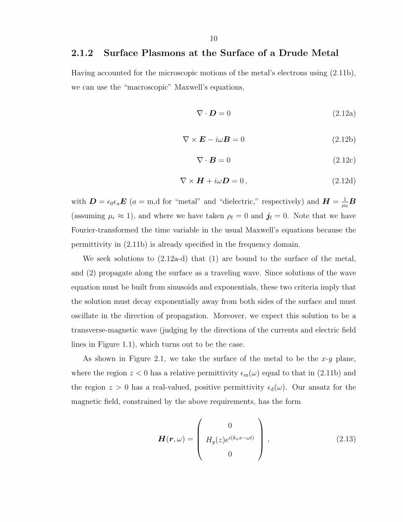
As shown in Figure 2.1, we take the surface of the metal to be the x-y plane,
where the region z < 0 has a relative permittivity εm(ω) equal to that in (2.11b) and
the region z > 0 has a real-valued, positive permittivity εd(ω). Our ansatz for the
magnetic field, constrained by the above requirements, has the form
H(r, ω) =
0
Hy(z)ei(kxx−ωt)
0
, (2.13)

11
Figure 2.1: Mode profile of a single-interface surface plasmon.
where we have taken the direction of propagation to be parallel to the x-axis. For H
to decay exponentially away from the surface, we require that
Hy(z) =
Hy,0 e−k(d)
z z z > 0
Hy,0 ek
(m)z z z < 0
, (2.14)
where kdz , k
mz > 0 are the wavevectors that describe the decay of H into the dielectric
and metal, respectively, and Hy,0 is a constant. From this ansatz we can calculate
the electric field using (2.12d):
∇×H = −iωD = −iωε0εaE
E =−1
iωε0εa
−H ′y(z)ei(kxx−ωt)
0
ikxHy(z)ei(kxx−ωt)
, (2.15)
where a = m,d in the metal and dielectric, respectively.
Taking the curl of (2.12d) and noting that ∇ ·H = 0, we have
−∇2H =ω2
c2εaH , (2.16)
12
where again, a = m,d. Substituting (2.13) gives the pair of relations
(k(d)z )2 = k2
x − εdω2
c2(2.17a)
(k(m)z )2 = k2
x − εmω2
c2, (2.17b)
which specify the 1/e decay lengths of the fields away from the surface of the metal.
Moreover, requiring that the x-component of E be continuous across the surface
yields the surface plasmon’s dispersion relation:
kx =ω
c
√εmεdεm + εd
. (2.18)
The quantity k0 ≡ ω/c is the wavevector of a free-space wave with the same frequency
as our plasmon. The factor (εmεd/(εm + εd))1/2, with εm given by (2.11b), is therefore
responsible for the wave’s dispersion.
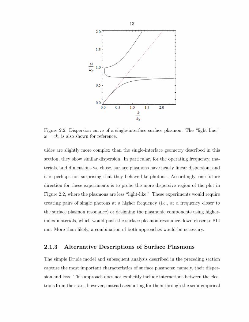
Figure 2.2 shows a plot of (2.18), where ω and kx have been normalized by ωp and
kp = ωp/c, respectively, and where ωp is as defined in (2.11b). In this calculation, the
dielectric is taken to be vacuum (i.e., εd = 1), and the Drude damping parameter,
γ, is set to ωp/10 for the sake of illustrating the model. The dotted line shows the
dispersion relation of light in vacuum, ω = ck. At low frequencies, surface plasmons
look a lot like photons, at least in terms of their dispersion. At frequencies closer
to the surface plasmon resonance (the horizontal asymptote at ωp/√
2), however, the
surface plasmon’s wavevector is substantially larger (and its wavelength therefore
much smaller) than that of a free-space wave of the same frequency. This effect is
the root of the technological interest in plasmonics: light can be confined to smaller
dimensions in plasmonic structures than in dielectric ones, shrinking the minimum
sizes of optical devices and increasing the strength of interactions between light and
matter.
In the experiments described in this thesis, my collaborators and I used single pho-
tons with a free-space wavelength of 814 nm to launch surface plasmons in dielectric-
loaded surface plasmon polariton waveguides (DLSPPWs). Although these waveg-
13
Figure 2.2: Dispersion curve of a single-interface surface plasmon. The “light line,”ω = ck, is also shown for reference.
uides are slightly more complex than the single-interface geometry described in this
section, they show similar dispersion. In particular, for the operating frequency, ma-
terials, and dimensions we chose, surface plasmons have nearly linear dispersion, and
it is perhaps not surprising that they behave like photons. Accordingly, one future
direction for these experiments is to probe the more dispersive region of the plot in
Figure 2.2, where the plasmons are less “light-like.” These experiments would require
creating pairs of single photons at a higher frequency (i.e., at a frequency closer to
the surface plasmon resonance) or designing the plasmonic components using higher-
index materials, which would push the surface plasmon resonance down closer to 814
nm. More than likely, a combination of both approaches would be necessary.
2.1.3 Alternative Descriptions of Surface Plasmons
The simple Drude model and subsequent analysis described in the preceding section
capture the most important characteristics of surface plasmons: namely, their disper-
sion and loss. This approach does not explicitly include interactions between the elec-
trons from the start, however, instead accounting for them through the semi-empirical
14
Drude damping parameter. More rigorous approaches account for electron-electron
interactions explicitly, as by modeling the electron density in a metal as a negatively-
charged fluid (hydrodynamic models) or by solving the Schrodinger equation using a
Hamiltonian that includes Coulomb interactions (the random-phase approximation,
time-dependent density functional theory). This thesis does not include any further
analysis by these methods, and I mention them here only for completeness. For an
extensive review of these theories and others, please see ref. [27].
2.2 Surface Plasmons in Quantum Theory
In classical theory, surface plasmons (more appropriately, “surface plasma waves”),
like any other waves, are infinitely divisible. That is, the amplitude of the wave—and
hence, the amount of energy or momentum stored in it—is a continuous parameter,
to which or from which it is always possible to add or subtract an arbitrary amount
(provided that the result is nonnegative, in the case of subtraction). In quantum
theory, in contrast, excitations of surface plasma waves come in discrete steps, i.e.,
surface plasmons. Like photons, individual surface plasmons are indivisible and must
be added to or subtracted from surface plasma waves in integer multiples. The fol-
lowing sections make these ideas more precise.
2.2.1 Quantization of the Free-Space Electromagnetic Field
In the Coulomb gauge, ∇·A = 0, and with no sources, Maxwell’s equations in vacuum
reduce to a single wave equation for the vector potential,
1
c2
∂2A
∂t2−∇2A = 0 , (2.19)
where E = −∂A∂t
and B = ∇×A. To find suitable boundary conditions, we consider
a large cubic box with edge length L and require A to be periodic at its faces. Inside
15
the box, solutions to (2.19) have the form
A(r, t) =∑k,n
ek,n[Ak,ne
i(k·r−ωkt) + A∗k,ne−i(k·r−ωkt)
], (2.20)
where ek,n (n ∈ {1, 2}) are orthonormal polarization vectors, k is constrained to a
discrete set of allowed values,
k =2π
L(mx,my,mz) , mx,my,mz ∈ {0,±1,±2, . . .} , (2.21)
and the frequencies in the complex exponentials are ωk = c|k|. Notice that the gauge
condition ∇ ·A = 0 implies that k · ek,n = 0; that is, the vector field A is a sum of
transverse waves. Equation (2.20) implies that the fields are
E(r, t) = i∑k,n
ωkek,n[Ak,ne
i(k·r−ωkt) + A∗k,ne−i(k·r−ωkt)
](2.22a)
B(r, t) =i
c
∑k,n
ωk(κ× ek,n)[Ak,ne
i(k·r−ωkt) + A∗k,ne−i(k·r−ωkt)
], (2.22b)
where κ = k/|k|. The energy stored in the fields is then
H =1
2
∫V
(ε0E ·E +
1
µ0
B ·B)d3r , (2.23)
where the integral is taken over the entire discretization box (x, y, z ∈ [0, L]). Substi-
tuting (2.22a,b) into (2.23) gives
H = 2ε0V∑k,n
ω2kA∗k,nAk,n , (2.24)
where we have taken advantage of the fact that the modes are orthogonal:
∫V
ei(k−k′)·rd3r = V δk,k′ . (2.25)
16
With a simple transformation of the variables Ak,n and A∗k,n,
Ak,n =1
2ωk(ε0V )1/2(ωkqk,n + ipk,n) (2.26a)
A∗k,n =1
2ωk(ε0V )1/2(ωkqk,n − ipk,n) , (2.26b)
eq. (2.24) transforms to
H = 2ε0V∑k,n
(p2k,n + ω2
k q2k,n) , (2.27)
which is the Hamiltonian of a collection of harmonic oscillators with frequencies ωk.
The key point is that, under this change of variables, each mode (i.e., frequency
component) of the free-space field looks like an independent harmonic oscillator.
To quantize the electromagnetic field, then, we substitute the quantum opera-
tors pk,n and qk,n for the classical amplitudes pk,n and qk,n and impose the usual
commutation relations:
[qk,n, pk′,n′ ] = ih δk,k′δn,n′
[qk,n, qk′,n′ ] = [pk,n, pk′,n′ ] = 0 .(2.28)
The classical amplitudes A∗k,n and Ak,n are now the creation and annihilation opera-
tors, respectively, for the mode with wavevector k and polarization n,
ak,n =1
2ωk(ε0V )1/2(ωkqk,n + ipk,n) (2.29a)
a†k,n =1
2ωk(ε0V )1/2(ωkqk,n − ipk,n) , (2.29b)
while (2.27) takes the form
H =∑k,n
(a†k,nak,n +
1
2
). (2.30)
17
Finally, the quantized fields are:
A(r, t) =∑k,n
(h
2ε0ωkV
) 12
ek,n
[ak,ne
i(k·r−ωkt) + a†k,ne−i(k·r−ωkt)
](2.31a)
E(r, t) = i∑k,n
(hωk
2ε0V
) 12
ek,n
[ak,ne
i(k·r−ωkt) − a†k,ne−i(k·r−ωkt)
](2.31b)
B(r, t) =i
c
∑k,n
(hωk
2ε0V
) 12
(κ× ek,n)[ak,ne
i(k·r−ωkt) − a†k,ne−i(k·r−ωkt)
]. (2.31c)
In these expressions, the correspondence between the classical field amplitudes and the
quantum creation and annihilation operators is clear. In particular, in studying many
problems in quantum optics (including two-photon quantum interference), it helps to
keep in mind that manipulations of the positive- and negative-frequency components
of the classical field E, for example, correspond to analogous manipulations of the
operators a and a†.
The operators a and a†, and their linear combinations, A, E, and B, operate
on a quantum state that describes the initial configuration2 of the fields. The most
convenient way to write this state is in the basis of Fock states,
F = {|n1〉 ⊗ |n2〉 ⊗ |n3〉 . . . | nj ∈ {0, 1, 2, . . .}} , (2.32)
where nj is the occupation number of the jth harmonic oscillator (“the number of
photons in mode j”), and each value of the index j stands for a distinct mode, that
is, a distinct combination of wavevector, k, and polarization, n. Each state |nj〉 is
related to the states |nj + 1〉 and (for nj > 0) |nj − 1〉 by the usual relations:
aj |nj〉 =√nj |nj − 1〉 (nj > 0) (2.33a)
a†j |nj〉 =√nj + 1 |nj + 1〉 . (2.33b)
These Fock states are sometimes written in the more compact form |n1 n2 n3 . . .〉, or,
2In other words, by quantizing the fields in this way we implicitly have been working in theHeisenberg picture.
18
more commonly, simply as
|n1 n2 n3 . . .〉 =1√n1!
(a1†)n1 1√
n2!
(a2†)n2 1√
n3!
(a3†)n3
. . . |0〉 , (2.34)
where |0〉 = |0 0 0 . . .〉 is the vacuum state—the state in which all oscillators are in their
ground states (i.e., the state in which there are no photons in any mode). A single
photon in the mode that has wavevector k and polarization n, for example, could be
written as |1k,n〉 = a†k,n |0〉. This notation is extremely useful for analyzing quantum
interference and entanglement with photons, because it allows us to describe the
dynamics of a mode in terms of the time evolution of that mode’s creation operator.
In quantum theory, then, each mode of the electromagnetic field looks like an
independent harmonic oscillator whose energy eigenstates each correspond to a well-
defined number of photons. When the mode is in its ground state it has zero photons,
when it is in its first excited state it contains exactly one photon, and so on. The
classical electric and magnetic fields are simply linear combinations of the creation
and annihilation operators for these modes, so manipulations of the fields in classical
theory correspond to similar manipulations of these operators in quantum theory.
2.2.2 Quantization of Surface Plasmons
For surface plasmons, an exactly analogous procedure yields the same relationship
between the classical and quantum theories [28, 29]. In particular, the quantized
vector potential that describes the classical surface plasmon fields in (2.13–2.15) is
A(r, t) =∑k
(h
2ε0ωkL2
) 12 [φk(r)ake
i(k·r−ωkt) + φ∗k(r)a†ke−i(k·r−ωkt)
], (2.35)
where the quantization volume V is now an area L2, the sum is over wavevectors k
parallel to the metal’s surface, and the function
φk(r) =
(ik − |k|
k(d)z
z)e−k
(d)z z z > 0(
ik + |k|k
(m)z
z)ek
(m)z z z < 0
(2.36)
19
captures the exponential decay of the fields away from the surface. The wavevectors
k(d)z and k
(m)z that characterize this decay are the same as those in (2.17a) and (2.17b).
The operators ak and a†k obey the commutation relation in (2.28) and act upon
Fock states as in (2.33a) and (2.33b). We can therefore picture surface plasmons
as directly analogous to photons: they are the indivisible quanta of modes of the
electromagnetic field, created and destroyed by operators that resemble the classical
field amplitudes in their dynamics. From this perspective, surface plasmons ought
to reproduce all of the same quantum effects that photons do, including quantum
interference and entanglement.
2.2.3 Experiments in Quantum Plasmonics
With the theoretical foundation laid as described in the previous section, it is up to
experiments either to verify these predictions or to determine that a more complex
model is needed. In all experiments so far,3 including those contributed in this thesis,
surface plasmons have been found to behave exactly as expected, exhibiting the same
quantum effects as photons.
For example, one set of experiments has shown that single photons and single-
photon emitters can be used to excite single surface plasmons. Whether excited by
a single quantum dot [32, 33], a single nitrogen-vacancy center in diamond [34], or
a single photon from a spontaneous parametric down-conversion source [35], single
surface plasmons exhibit the same “anti-bunching” that single photons do. In these
experiments, a single plasmon is given two equally accessible paths, each monitored
by a separate detector. The detectors each click with roughly the same frequency but
never simultaneously, indicating that in each trial the plasmon is only found in one
of the two paths and confirming that there indeed was only one plasmon in the first
place. These experiments thus validate the notion of single-plasmon Fock states.
Another set of experiments has demonstrated quantum entanglement between sur-
face plasmons. In the earliest experiment of this type, Altewischer and co-workers
3See refs. [30, 31] for recent reviews of the field.
20
created a pair of polarization-entangled photons, sent one or both through a plasmonic
hole array in a metal film, and verified that they remained entangled [36, 37]. Later,
Fasel and collaborators performed similar experiments with frequency-entangled pho-
tons transmitted through plasmonic hole arrays [38] and long-range surface plasmon
polariton (LRSPP) waveguides [39], verifying in both cases the perseverance of the
entangled state.
These experiments and others have verified that surface plasmons do indeed ex-
hibit several of the familiar phenomena from quantum optics, including single-photon
statistics, polarization and frequency entanglement, and squeezing [40]. Missing from
this list, however, are two-photon quantum interference and path entanglement. The
former effect requires not only that a pair of single plasmons exhibit nonclassical
statistics but also that they remain indistinguishable and mutually coherent. The
latter effect involves preparing a state in which two surface plasmons are superposed
between a pair of waveguides such that neither is definitely in one waveguide or the
other, but as soon as one is measured (hypothetically), the other is known to be
in the same waveguide. In this case, any interaction (other than absorption) be-
tween the plasmons and the metal that supports them ought to cause decoherence.
In other words, the metal needs only to distinguish between their mere presence or
absence, rather than between states of their polarization or frequencies. Experiments
demonstrating these effects are the subject of this thesis.
2.3 Two-Photon Quantum Interference
Underlying both of the experiments that my collaborators and I performed is the
phenomenon of two-photon quantum interference (TPQI) [41]. This effect involves
two photons entering adjacent inputs of a 50-50 beam splitter, where each can be
routed to either of the two outputs. If the photons are indistinguishable in every
degree of freedom (polarization, spectrum, arrival time at the splitter, spatial overlap
at the splitter), the quantum probability amplitudes that correspond to the cases
where both are transmitted or both are reflected cancel each other, leaving only the
21
possibility that both emerge from the splitter together in one output or the other.
Because this effect forms the foundation of the experiments described in this thesis,
we review it briefly in this section.
2.3.1 Beam Splitters in Quantum Optics
In classical optics, it is possible to describe the action of a beam splitter by a 2 × 2
matrix that maps two incoming modes to two outgoing modes. We assume that the
splitter consists only of isotropic, linear materials, so the polarization and frequency
of the output light must match those of the input light. Under these assumptions, the
input waves E1ei(k1·r−ωt) and E2e
i(k2·r−ωt) are fully described simply by their complex
scalar amplitudes, E1 and E2. At a symmetric 50-50 beam splitter, they are related
to the output waves E3 (opposite input 1) and E4 (opposite input 2) as follows:
E3
E4
=1√2
1 i
i 1
E1
E2
. (2.37)
The top line of this equation, E3 = 1√2(E1 + iE2), states that the wave in output 3
consists of the transmitted half of the wave from input 1 (with zero relative phase)
and the reflected half of the wave from input 2, which undergoes a π/2 phase shift
upon reflection.4 The bottom line gives a similar expression for the wave emerging
from output 4. The first diagram in Figure 2.3 shows how the beam splitter mixes
these (classical) waves.
The quantum theory of a beam splitter is identical, except that annihilation oper-
ators, aj, replace the classical mode amplitudes, Ej, as shown in the second diagram
in Figure 2.3. This substitution reflects the general correspondence between a given
mode’s complex field amplitudes in classical theory and its creation and annihilation
4It turns out that this phase shift is required by energy conservation in any symmetric 50-50splitter [42].

22
Figure 2.3: A beam splitter in classical (left) and quantum (right) theory.
operators in quantum theory, as in (2.31b). Explicitly, (2.37) takes the form
a3
a4
=1√2
1 i
i 1
a1
a2
, (2.38)
where aj is the annihilation operator for the jth input or output mode.
Despite the conceptual similarity between equations (2.37) and (2.38), they make
very different predictions in some cases. In the case that a classical wave enters
input 1 while none enters input 2, for example, eq. (2.37) says that the wave is split
evenly between the two outputs: E3 = 1√2E1 and E4 = i√
2E1. In contrast, if a single
photon enters input 1, quantum theory predicts a qualitatively different result,
|Ψin〉 = a†1|0〉 → 1√2
(a†3 + i a†4)|0〉 =1√2
(|1, 0〉+ i |0, 1〉) , (2.39)
where the output state |m,n〉 indicates that there are m photons in output 3 and n
in output 4, and the substitution a†1 → 1√2(a†3 + i a†4) comes from inverting (2.38) and
taking its conjugate. The output state in (2.39) indicates that the photon does not
have a well-defined position until a measurement is made, but once that happens it
is equally likely to be found in either output.
How is it possible to distinguish the classical experiment from the quantum one?
After all, in both cases one would record equal intensities in both of the beam splitter’s
outputs after averaging over many trials. Indeed, in any experiment involving only
23
one photon, measurements of the intensity of the field can never tell the difference
between the predictions of the classical and quantum theories.
The trick in this case is to measure the correlation between the intensities at the
two outputs of the beam splitter. This can be done by placing a detector at each
output and recording the number of simultaneous counts. In the classical case, the
wave is split evenly between the two outputs, so both detectors register a signal. In
the quantum case, however, measurements of the output state in (2.39) only ever find
the photon in one output or the other, so the detectors never click simultaneously.
The absence of coincident counts is proof that single photons were in fact measured,
as opposed to very weak classical waves.
The general strategy outlined in this simple example—write the input state as a
sequence of creation operators acting on the vacuum, transform the operators accord-
ing to the classical matrix describing the beam splitter, and compute the resulting
state—is equally applicable in any case involving beam splitters operating on quan-
tized fields. We next apply it to the case of two input photons and observe quantum
interference as a result.
2.3.2 A Simple Single-Frequency Model of TPQI
What happens when two photons enter a 50-50 beam splitter simultaneously, one in
each input? If the photons are identical and the beams that carry them overlap at
the splitter, it is possible to use the simple single-frequency, single-mode theory from
the previous section. In particular, we take the input state to be |1, 1〉 = a†1a†2|0〉 and
use (2.38) to write a†1 and a†2 in terms of the operators for the output modes:
|Ψin〉 = a†1a†2|0〉 → 1
2(a†3 + i a†4)(i a†3 + a†4)|0〉 =
i√2
(|2, 0〉+ |0, 2〉) , (2.40)
Notice that the terms involving the product a†3a†4 have canceled each other, leaving
no component of the final state with one photon in each output. This is two-photon
quantum interference, which can be measured by placing a detector at each output
of the beam splitter and verifying that the detectors never click simultaneously.

24
How best to interpret this effect? The two states a†3a†4|0〉 and −a†4a
†3|0〉 represent
cases in which both photons are either transmitted or reflected at the beam split-
ter, respectively. (The π phase shift—i.e., the minus sign—that multiplies the latter
state comes from two factors of the π/2 phase shift from the beam splitter matrix
in (2.37) and (2.38), which are required for a lossless splitter by energy conserva-
tion.5) We therefore understand TPQI as a superposition and cancellation (i.e., an
“interference”) between two of the four possible outcomes of the experiment, namely
those that involve both photons being transmitted or both being reflected. This view
fits naturally with the path-integral formulation of quantum mechanics developed by
Dirac and Feynman: in the sum over all possible trajectories of the system, these two
components cancel, leaving only the two outcomes in which both photons are found
together in one output or the other.
Of course, this cancellation only occurs if the state corresponding to both photons
being transmitted at the splitter is in fact the same as the state in which both are
reflected. In this simple model, these states are guaranteed to be identical because we
have only included a single frequency and polarization, and we have stipulated that
the spatial modes of the photons overlap at the beam splitter. In a real experiment,
however, the photons might have slightly different spectra, polarizations, or spatial
modes, in which case perfect quantum interference would not occur. To describe this
case, a more complex model is necessary.
2.3.3 Multi-Frequency TPQI
Following ref. [41], we begin by writing the two-photon state that results from spon-
taneous parametric down-conversion as a general superposition of two-photon states
of different frequencies:
|Ψ〉 =
∫ ∞−∞
φ(ω, ωp − ω) |ω, ωp − ω〉 dω . (2.41)
5See [42] for the classical theory of a lossless beam splitter. See also Section 4.2 for the details ofTPQI in lossy splitters.

25
Here, φ(ωs, ωi) is a spectral weight function that depends on the specific details of
phase-matching in the nonlinear crystal and any subsequent spectral filtering. We
assume that it is real and symmetric about a maximum at ωs = ωi = ωp/2. We
also assume that it decays to zero far from this value. The probability of finding one
photon in each of the beam splitter’s outputs (labeled “3” and “4” for consistency
with the previous sections) at times t and t+ τ is:
Pcoinc(τ) = 〈Ψ|E(−)3 (t)E
(−)4 (t+ τ)E
(+)4 (t+ τ)E
(+)3 (t)|Ψ〉
∝ 〈Ψ|a3(t)a4(t+ τ)a†4(t+ τ)a†3(t)|Ψ〉 .(2.42)
Writing a3 and a4 in terms of a1 and a2, as in the previous sections, it follows that
the joint detection probability is
Pcoinc(τ) =1
4|G(0)|2
{|g(τ)|2 + |g(2δτ − τ)|2 − [g∗(τ)g(2δτ − τ) + g(τ)g∗(2δτ − τ)]
},
(2.43)
where G(τ) is the Fourier transform of φ,
G(τ) =
∫ ∞−∞
φ(ωp
2+ ω,
ωp
2− ω
)e−iωτdω , (2.44)
and g(τ) is a normalized version of the same function, g(τ) = G(τ)/G(0). The
quantity δτ is the delay between the arrival of the two photons at the beam splitter.
Because we assume that φ(ωs, ωi) decays to zero far from its peak at ωs = ωi =
ωp/2, the correlation function g(τ) drops to zero for τ larger than a characteristic
time. Physically, this is the photons’ mutual coherence time. In many experiments,
including those described in Chapters 4 and 5, this time is much shorter than what
single photon detectors can resolve.6 As a result, the integral of Pcoinc(τ) over the
detection interval is well approximated by the integral of this quantity over all τ :
Pcoinc ≈∫ ∞−∞
Pcoinc(τ) dτ =1
2
[1−
∫∞−∞ g(τ) g(τ − 2δτ) dτ∫∞
−∞ (g(τ))2 dτ
]. (2.45)
6For an interesting case where the photons’ coherence time is much longer than the detectors’resolution, see refs. [43] and [44].

26
In particular, Pcoinc drops to zero for δτ = 0. For δτ much larger than the coherence
time, we have∫∞−∞ g(τ) g(τ − 2δτ) dτ = 0 and, as a consequence, Pcoinc approaches a
constant value of 1/2.
In many cases, including the experiments my collaborators and I performed, the
spectral weight function φ(ωs, ωi), and hence the correlation function g(τ), are deter-
mined by narrow-bandwidth optical filters. Modeling the transmission spectrum of
these (identical) filters as a Gaussian with bandwidth ∆ω, a decent approximation in
our case, the correlation function becomes simply
g(τ) = e−12
(∆ω τ)2
, (2.46)
and (2.45) reduces to
Pcoinc =1
2
[1− e−(∆ω δτ)2
]. (2.47)
That is, the coincidence detection probability is an inverted Gaussian function with
temporal width (∆ω)−1. This type of measurement thus reveals not only whether or
not the two photons are identical, which affects the depth of the “Hong-Ou-Mandel
dip” described by this function, but also what their coherence time is. In our measure-
ments of plasmonic TPQI (see Chapter 4), we were interested both in whether or not
plasmons exhibited this effect and whether or not their coherence times diminished
compared to the photons that excited them.
2.4 Spontaneous Parametric Down-Conversion
Spontaneous parametric down-conversion (SPDC) is a χ(2) nonlinear optical process
in which a pump laser of frequency ωp generates two beams of light, the “signal” and
“idler,” with frequencies ωs and ωi such that ωs + ωi = ωp. In our case, we were
interested in degenerate SPDC, where the signal and idler were identical: ωs = ωi =
12ωp. In the context of quantum mechanics this frequency conversion happens photon-
by-photon, so the down-converted beams represent pairs of single photons to a good
approximation, as long as the pump laser is not too powerful. More precisely, each
27
beam independently shows thermal statistics [45], but measurements of one beam
conditioned on detecting a photon in the second beam reveal single-photon statistics,
again as long as the pump laser power is not too high.
Microscopically, SPDC (and all other nonlinear processes) originate from the non-
linear dependence of the polarization on the electric field:
Pi = ε0
(χiEi + χ
(2)ij EiEj + χ
(3)ijkEiEjEk + . . .
)= ε0χiEi + PNL
i . (2.48)
In this expression, χ is the ordinary linear susceptibility, χ(2) is the second-order
nonlinear susceptibility tensor, and so on. The quantity PNL captures the nonlinear
dependence of P on E and is small compared to the linear component of P .
From Maxwell’s equations with no sources (i.e., ρf = 0, Jf = 0),
∇2E − εrc2
∂2E
∂t2= µ0
∂2PNL
∂t2, (2.49)
where εr = 1 +χ. The nonlinear polarization, PNL, thus acts as a source in the wave
equation forE. In particular, ifE has components that oscillate at frequencies ω1 and
ω2, then the term proportional to χ(2) in (2.48) implies that there will be components
of P oscillating at ω1+ω2 and ω1−ω2 as well. According to (2.49), these polarizations
act like sources for waves at these frequencies. In a nonlinear material, then, waves
can interact with one another, generating new waves at different frequencies [46].
One subtlety of spontaneous parametric down-conversion is that it is necessary
to invoke the quantum mechanical notion of a “vacuum field” to apply the reasoning
of the previous paragraph. The “wave” oscillating at frequency ω2 is taken to be
the vacuum field, which, given a pump wave of frequency ω1, produces a polarization
oscillating at ω1−ω2. Since there are vacuum fluctuations at all frequencies, the single
input pump wave generates components of the nonlinear polarization oscillating at
all frequencies as well.7 This effect is exactly analogous to the spontaneous emission
of an excited emitter; instead of driving an electronic transition of an excited emitter,
7In a real material, though, the nonlinear coefficients χ(2), χ(3)), etc. depend on frequency andset the range of allowed operating frequencies.

28
in this case the vacuum field drives the conversion of a photon at a higher frequency
to a pair of photons at lower frequencies.
An intuitive physical picture helps to interpret (2.49). A pump wave and signal
wave (the vacuum field, in SPDC) together induce microscopic dipoles throughout
the material to oscillate at the sum and difference frequencies, and, under the right
conditions, the waves that these dipoles emit add constructively to produce a mea-
surable output. What conditions ensure constructive interference? It turns out (see
ref. [46]) that the wave vectors of the signal and idler waves must sum to the pump
wave vector. Together with the constraint on the frequencies of these waves, we have
ωs + ωi = ωp , (2.50a)
ks + ki = kp . (2.50b)
Simultaneously satisfying these equations is difficult because, in most materials, the
index of refraction (and hence the magnitude of k) increases slightly with increasing
frequency. In SPDC, the sum |ks| + |ki| is therefore slightly less than |kp|, and it
is impossible to satisfy (2.50b) for any choice of the orientations of the three wave
vectors.
The most common solution to this “phase-matching” problem is to choose a non-
linear material that is also birefringent. This way, it is possible to choose the polar-
izations and directions of the signal and idler waves such that at least one of them
experiences a higher refractive index than the pump wave. It is therefore possible to
satisfy (2.50b) for a particular choice of the pump, signal, and idler frequencies.
29
Chapter 3
Experimental Design and Methods
3.1 Design of Dielectric and Plasmonic Compo-
nents
The experiments described in Chapters 4 and 5 relied on the same underlying technol-
ogy: a silicon nitride-based photonics platform with integrated plasmonic waveguides.
This section describes the design and fabrication of these components, highlighting
the constraints and trade-offs involved in choosing this approach as well as some of
the technical challenges encountered along the way.
3.1.1 Design Constraints
My collaborators and I faced a number of design decisions early on that shaped
the development of these experiments. The questions of which operating frequency,
waveguide materials, and single-photon source/detectors to use were all interrelated,
requiring that our experimental plan address all of these issues at the outset before
we could begin to make progress on any individual experimental goal.
As it turned out, the most important factor in making these decisions was that we
needed to be able to generate and detect single photons using commercially available
equipment. Spontaneous parametric down-conversion (SPDC) was the clear choice
as a source of photon pairs, offering high-intensity, mutually coherent beams of single
photons and suffering none of the drawbacks of sources based on single molecules [47]
30
or quantum dots [48, 49]. The highest-efficiency single-photon detectors available for
purchase at the time were made of silicon, limiting the choice of wavelengths for our
single photons to the range 500-900 nm. Ion and diode lasers, convenient candidates
to pump the SPDC source, were only available down to 350 nm, which further limited
the down-converted photons to the range 700-900 nm.
Taking these factors into consideration, and as a compromise between higher loss
in plasmonic waveguides at 700 nm and lower detection efficiency at 900 nm, we finally
decided that our operating wavelength should be close to 800 nm. As inexpensive,
high-powered InGaN diode lasers were available at 405 nm, we chose 810 nm for
the down-converted photons. More precisely, the particular InGaN diode laser we
bought actually had a wavelength of 407 nm, so the down-converted photons had a
wavelength of 814 nm. At this wavelength, our detectors (τ -SPAD, by PicoQuant)
were > 50% efficient and losses in our plasmonic waveguides, though substantial, were
not overwhelming.
3.1.2 Waveguides
With the operating wavelength set in this way by the source and detectors, we next
had to decide on a general approach to take for making the measurement. Naturally,
a key factor in this decision was how efficiently light could be coupled into and out
of plasmonic waveguides in different configurations. Other groups had launched plas-
mons in waveguides by direct end-fire coupling [50] or by focusing light onto gratings
[33], but neither strategy offered high enough coupling efficiency for our experiments.
Another approach, which achieved high coupling efficiency between free space and
metal-insulator-metal slot waveguides at 1550 nm using antenna couplers [51, 52],
was unsuitable for our experiments because propagation loss in these waveguides
would be too high at 814 nm.
Luckily, a recent graduate of the Atwater group, Dr. Ryan Briggs, had devised a
way to efficiently couple silicon waveguides directly to dielectic loaded surface plas-
mon polariton waveguides (DLSPPWs) with coupling losses of less than 1 dB (i.e.,
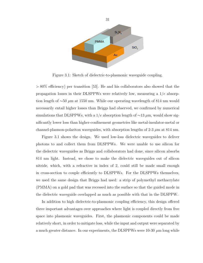
31
Figure 3.1: Sketch of dielectric-to-plasmonic waveguide coupling.
> 80% efficiency) per transition [53]. He and his collaborators also showed that the
propagation losses in their DLSPPWs were relatively low, measuring a 1/e absorp-
tion length of ∼50 µm at 1550 nm. While our operating wavelength of 814 nm would
necessarily entail higher losses than Briggs had observed, we confirmed by numerical
simulations that DLSPPWs, with a 1/e absorption length of ∼13 µm, would show sig-
nificantly lower loss than higher-confinement geometries like metal-insulator-metal or
channel-plasmon-polariton waveguides, with absorption lengths of 2-3 µm at 814 nm.
Figure 3.1 shows the design. We used low-loss dielectric waveguides to deliver
photons to and collect them from DLSPPWs. We were unable to use silicon for
the dielectric waveguides as Briggs and collaborators had done, since silicon absorbs
814 nm light. Instead, we chose to make the dielectric waveguides out of silicon
nitride, which, with a refractive in index of 2, could still be made small enough
in cross-section to couple efficiently to DLSPPWs. For the DLSPPWs themselves,
we used the same design that Briggs had used: a strip of polymethyl methacrylate
(PMMA) on a gold pad that was recessed into the surface so that the guided mode in
the dielectric waveguide overlapped as much as possible with that in the DLSPPW.
In addition to high dielectric-to-plasmonic coupling efficiency, this design offered
three important advantages over approaches where light is coupled directly from free
space into plasmonic waveguides. First, the plasmonic components could be made
relatively short, in order to mitigate loss, while the input and output were separated by
a much greater distance. In our experiments, the DLSPPWs were 10-30 µm long while

32
the dielectric waveguides were several millimeters in length. By keeping the input and
output to the circuit separated by such a large distance, we could guarantee that all
the light collected at the output had actually traversed the waveguides, as opposed
to scattering straight from the input to the output. Had we tried to excite plasmons
directly from free space using gratings or antennas, it would have been more difficult
to isolate the output from scattered light without making the plasmonic waveguides
longer.
Second, the problem of coupling light into dielectric waveguides had been studied
more thoroughly than that of coupling from free space to plasmonic waveguides,
with typical coupling efficiencies correspondingly higher in the dielectric case. For
example, both end-fire couplers [54, 55] and grating couplers [56, 57] with greater
than 80 % coupling efficiency per transition have been proposed and experimentally
demonstrated. Between these two alternatives, end-fire couplers promised higher
coupling efficiency and a simpler design given the materials and wavelength we chose
to use.
Finally, using dielectric waveguides to deliver single photons to and collect them
from plasmonic parts allowed us to build more complex circuits than would have been
possible had we decided to couple light directly from free space into plasmonic waveg-
uides. In the path-entanglement experiment, for example, we built a Mach-Zehnder
interferometer entirely out of dielectric waveguides before integrating the plasmonic
components. While constructing such an interferometer in free space would not have
been particularly challenging, the task of integrating a pair of plasmonic waveguides
without introducing unbalanced losses (i.e., unequal coupling efficiencies) in the two
arms of the interferometer would have been considerably more difficult. Fabricating
the entire interferometer on a silicon chip, we were able to control the dimensions and
relative positions of the components to achieve a high degree of uniformity, which
ensured that coupling losses at the plasmonic waveguides were usually well-balanced.
Figure 3.2 shows cross-sections of the dielectric and plasmonic waveguides we
designed. The dielectric waveguide comprised a silicon nitride core that was 400 nm
wide and 280 nm tall clad below by thermal silicon dioxide and on the other three
33
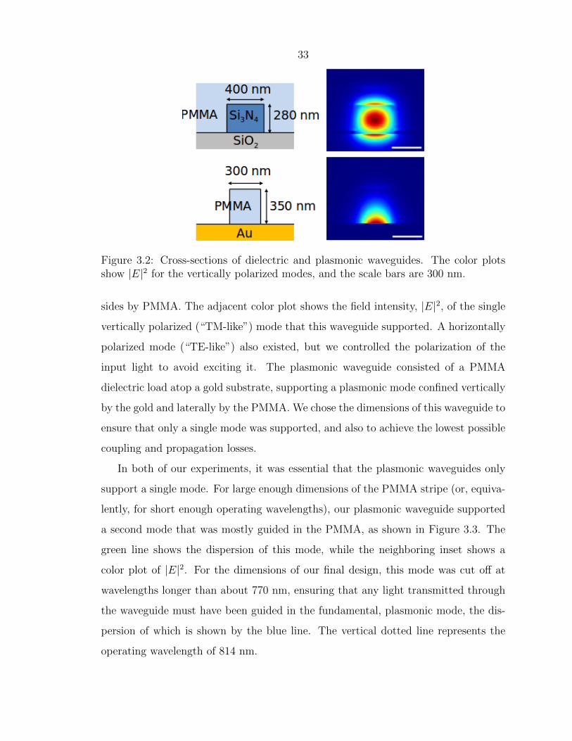
Figure 3.2: Cross-sections of dielectric and plasmonic waveguides. The color plotsshow |E|2 for the vertically polarized modes, and the scale bars are 300 nm.
sides by PMMA. The adjacent color plot shows the field intensity, |E|2, of the single
vertically polarized (“TM-like”) mode that this waveguide supported. A horizontally
polarized mode (“TE-like”) also existed, but we controlled the polarization of the
input light to avoid exciting it. The plasmonic waveguide consisted of a PMMA
dielectric load atop a gold substrate, supporting a plasmonic mode confined vertically
by the gold and laterally by the PMMA. We chose the dimensions of this waveguide to
ensure that only a single mode was supported, and also to achieve the lowest possible
coupling and propagation losses.
In both of our experiments, it was essential that the plasmonic waveguides only
support a single mode. For large enough dimensions of the PMMA stripe (or, equiva-
lently, for short enough operating wavelengths), our plasmonic waveguide supported
a second mode that was mostly guided in the PMMA, as shown in Figure 3.3. The
green line shows the dispersion of this mode, while the neighboring inset shows a
color plot of |E|2. For the dimensions of our final design, this mode was cut off at
wavelengths longer than about 770 nm, ensuring that any light transmitted through
the waveguide must have been guided in the fundamental, plasmonic mode, the dis-
persion of which is shown by the blue line. The vertical dotted line represents the
operating wavelength of 814 nm.

34
Figure 3.3: Dispersion of the fundamental plasmonic (blue line) and second-orderdielectric (green line) modes of the DLSPPWs. The red line denotes the refractiveindex of the single-interface surface plasmon at the gold-air interface.
We used a similar calculations to confirm that the dielectric waveguides we de-
signed also supported only one vertically polarized mode. This way, we could make
directional couplers and spot-size converters that would not have worked properly
with multimode waveguides.
3.1.3 50-50 Directional Couplers
A key component in our optical circuits was the 50-50 directional coupler, formed by
two parallel waveguides that are close enough to couple to one another. To mea-
sure plasmonic quantum interference we made a 50-50 directional coupler out of
DLSPPWs, while our second experiment required a pair of dielectric 50-50 couplers
that formed an interferometer. In both experiments, these couplers functioned as the
integrated-photonics equivalents of the 50-50 beam splitter described in Section 2.3.1.
Both the dielectric and plasmonic directional couplers operate according to the
same underlying principle. In either case, two parallel waveguides are brought close
to one another over a predetermined distance (several microns, in the case of our
dielectric couplers) so that the evanescent tail of each mode overlaps significantly with
the neighboring waveguide. The modes of the resulting pair of coupled waveguides
then resemble even and odd combinations of the modes of the individual, uncoupled
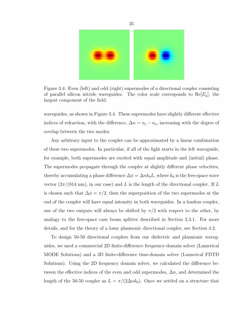
35
Figure 3.4: Even (left) and odd (right) supermodes of a directional coupler consistingof parallel silicon nitride waveguides. The color scale corresponds to Re[Ey], thelargest component of the field.
waveguides, as shown in Figure 3.4. These supermodes have slightly different effective
indices of refraction, with the difference, ∆n = ne− no, increasing with the degree of
overlap between the two modes.
Any arbitrary input to the coupler can be approximated by a linear combination
of these two supermodes. In particular, if all of the light starts in the left waveguide,
for example, both supermodes are excited with equal amplitude and (initial) phase.
The supermodes propagate through the coupler at slightly different phase velocities,
thereby accumulating a phase difference ∆φ = ∆nk0L, where k0 is the free-space wave
vector (2π/(814 nm), in our case) and L is the length of the directional coupler. If L
is chosen such that ∆φ = π/2, then the superposition of the two supermodes at the
end of the coupler will have equal intensity in both waveguides. In a lossless coupler,
one of the two outputs will always be shifted by π/2 with respect to the other, by
analogy to the free-space case beam splitter described in Section 2.3.1. For more
details, and for the theory of a lossy plasmonic directional coupler, see Section 4.2.
To design 50-50 directional couplers from our dielectric and plasmonic waveg-
uides, we used a commercial 2D finite-difference frequency-domain solver (Lumerical
MODE Solutions) and a 3D finite-difference time-domain solver (Lumerical FDTD
Solutions). Using the 2D frequency domain solver, we calculated the difference be-
tween the effective indices of the even and odd supermodes, ∆n, and determined the
length of the 50-50 coupler as L = π/(2∆nk0). Once we settled on a structure that

36
was feasible to fabricate—i.e., one with not too small a gap between the waveguides
and not too long a coupling length in the plasmonic case—we verified the design
using a full 3D FDTD simulation. More precisely, we checked to make sure that the
intensity of the input light was indeed split evenly between the two outputs, and that
the wave in one output was shifted in phase by π/2 with respect to that in the other
output. Recognizing that fabricated structures are never identical to simulated ones,
we fabricated several directional couplers with a range of coupling lengths near the
design length and performed measurements of two-photon quantum interference (see
Section 2.3) to identify the true 50-50 design.
3.1.4 Spot-Size Converters
A key challenge in any integrated photonics experiment is coupling light into and out
of waveguides efficiently enough to make a decent measurement. Low insertion loss
is especially crucial in quantum plasmonics, where the source is necessarily weak (so
that the probability of measuring multi-photon states is low) and the waveguides are
strongly absorbing.
Considering our operating wavelength and materials, end-fire coupling into spot-
size converters [54, 55] promised the best coupling efficiency and most straightforward
fabrication. While similarly high coupling efficiencies have been achieved in silicon
waveguides at 1550 nm with grating couplers [57], in our case the shorter operating
wavelength and lower refractive index of silicon nitride would make grating coupling
more challenging. Moreover, coupling from free space into spot-size converters al-
lows us to optimize the alignment of the two optical inputs (one for each photon)
independently.
We experimented with several designs for the spot-size converters, using planar
films and etched or patterned ridges of SiO2 and SU-8 resist, before finally settling
on patterned ridges of PMMA. Figure 3.5 shows two of the designs we considered
(bottom panels). In the lower left panel, the tapered end of the waveguide is covered
by a planar film of SiO2; in the right panel, it is covered by a PMMA waveguide whose
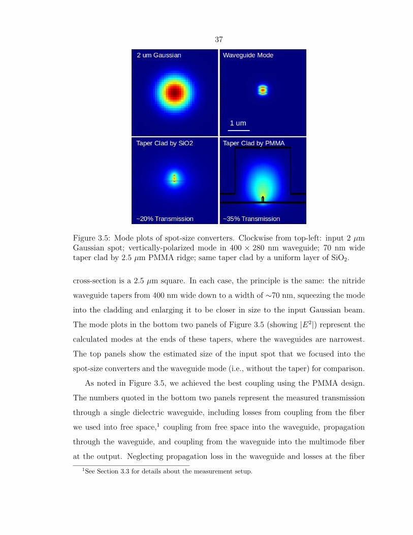
37
Figure 3.5: Mode plots of spot-size converters. Clockwise from top-left: input 2 µmGaussian spot; vertically-polarized mode in 400 × 280 nm waveguide; 70 nm widetaper clad by 2.5 µm PMMA ridge; same taper clad by a uniform layer of SiO2.
cross-section is a 2.5 µm square. In each case, the principle is the same: the nitride
waveguide tapers from 400 nm wide down to a width of ∼70 nm, squeezing the mode
into the cladding and enlarging it to be closer in size to the input Gaussian beam.
The mode plots in the bottom two panels of Figure 3.5 (showing |E2|) represent the
calculated modes at the ends of these tapers, where the waveguides are narrowest.
The top panels show the estimated size of the input spot that we focused into the
spot-size converters and the waveguide mode (i.e., without the taper) for comparison.
As noted in Figure 3.5, we achieved the best coupling using the PMMA design.
The numbers quoted in the bottom two panels represent the measured transmission
through a single dielectric waveguide, including losses from coupling from the fiber
we used into free space,1 coupling from free space into the waveguide, propagation
through the waveguide, and coupling from the waveguide into the multimode fiber
at the output. Neglecting propagation loss in the waveguide and losses at the fiber
1See Section 3.3 for details about the measurement setup.
38
collimator, and assuming that the coupling losses into and out of the waveguide
were comparable, this measurement indicates that we achieved a coupling efficiency
of about 60% per transition using the PMMA coupler, compared to about 45% per
transition with the oxide slab. We did not measure the transmission through a waveg-
uide without tapers (upper right panel of Figure 3.5), but finite-difference frequency
domain simulations indicate that the efficiency of coupling from a 2 µm Gaussian
spot into that mode would have been roughly a factor of three lower. Coupling out
of the waveguide and into the multimode fiber probably would have been less effi-
cient as well, since light coming from the tightly confined waveguide mode would
have diverged at a greater angle than light coming from the larger PMMA spot-size
converter.
3.1.5 Wafer-Level Design Considerations
Having chosen end-fire coupling for these measurements, the last major design deci-
sion was how best to dice the chips in order to get optical-quality end facets. This
straightforward-sounding task ultimately required substantial additional design work
and process development. Luckily, it was possible to perform the additional processes
on an entire 4” wafer at a time, amortizing the extra time across about two dozen
chips with nine dice each.
The silicon wafers I used for these chips had a 3 µm thermal SiO2 layer grown
on both sides, followed by a 300 nm Si3N4 layer. The thick oxide layer formed the
lower cladding of the waveguides, isolating their modes from the absorbing silicon
substrate. Unfortunately, scribing through this thick, dense layer using the Dynatex
scriber in the KNI did not work well consistently. Often, the scribe tip would not
quite reach the underlying silicon, or else would not make a continuous scribe mark
in it, and the chips would not cleave along the intended direction as a result.
Additionally, although I ordered the thinnest 4” wafers that were available, at
300 µm thick they still did not always cleave cleanly, even with good scribe marks. I
found that thinning them to ∼200 µm improved the tendency for the finished chips

39
Figure 3.6: Etched pattern to improve dicing yield. Scribing through the thick ther-mal oxide layer (left panel) often resulted in cleaving along an unpredictable curve(dotted red line) instead of parallel to the scribe mark (thick red line). Scribing di-rectly on the silicon (middle panel) where the oxide and nitride had been etched away(right panel) improved the yield of this step significantly.
Figure 3.7: Layout of chips on a 4” wafer. The black areas show the dicing pattern,where the nitride and oxide were removed. There are 27 chips on the wafer and ninedice on each chip.
to cleave as desired.
To achieve the best yield for the dicing step, I ultimately settled on the approach
illustrated in Figure 3.6. In the corners of each die I etched away the nitride and
oxide layers, allowing me to scribe directly on the silicon. Together with thinning the
wafers to ∼200 µm, this change improved the yield of this step from about 10% to
approximately 70%.
The cost of this improvement was a set of several additional processing steps, as
described in more detail in the next section. Briefly, it involved etching the pattern
shown in Figure 3.7 into a 4” wafer, all the way through the nitride and oxide layers
and down to the underlying silicon. The pattern contained 27 chips (left sketch), each
of which had nine dice (right sketch) on it. Typically, I would build nine identical
40
copies of an experiment on a chip, one per die, so as to end up with five or six
defect-free chips for measurements.
3.2 Fabrication Methods
The following sections give an essential overview of the process I used to fabricate
the chips my collaborators and I studied. For a detailed, step-by-step account of the
fabrication process, please see the Appendix.
3.2.1 Initial Full-Wafer Processing
I started with 4” silicon wafers on which a foundry2 had grown a 3 µm wet thermal
oxide layer and a 300 nm Si3N4 layer by low-pressure chemical vapor deposition
(LPCVD). The wafers themselves were initially 300 µm thick and were doped n-
type. Although our experiments imposed no particular requirements on the electronic
properties of the silicon, the doping type and concentration are still important because
they affect the etch rate of silicon in potassium hydroxide. In particular, heavily
doping silicon with boron reduces the etch rate significantly [58], but n-type dopants
do not make as great a difference.
I began by using photolithography and plasma etching to transfer the dicing pat-
tern of Figure 3.7 into the silicon nitride layer on the front of the wafer. I found
that there were two key tricks to ensure that this etch worked correctly: after the
photolithography step I hard-baked the photoresist, and during the etch step I used
PMMA to ensure good thermal contact between the device wafer and the carrier
wafer. These two extra steps helped prevent the resist from bubbling, cracking, or
flaking during the etch.
After etching the dicing pattern through the silicon nitride layer, the next step was
to remove the nitride and oxide layers from the back side of the wafer. This process
required two separate etches, a plasma etch for the nitride and a wet etch using
hydrofluoric acid to remove the oxide. Before each of these etches, it was important
2Rogue Valley Microdevices, Medford, OR.
41
to spin a thick layer (several microns) of photoresist on the front side of the wafer
to protect it, hard-baked as before to improve its etch resistance. Also, during the
hydrofluoric etch to remove the oxide, I found that it was best to float the wafer on
top of concentrated hydrofluoric acid, rather than submerging it and relying on the
resist to protect the front surface. Although HF does not attack most photoresists,
fluoride ions diffuse quickly through them and attack the material underneath. The
active species in buffered HF is HF2− rather than F−, so diffusion is substantially
slower. If this step is found to be difficult to reproduce, substituting buffered HF for
concentrated HF and etching for a correspondingly longer time should improve the
resistance of the photoresist.
Next, I etched the wafer in potassium hydroxide to thin it from 300 µm to 200 µm.
As the etch rate of silicon in KOH increases exponentially with temperature, I per-
formed this etch at 90-100◦C to reduce the amount of time required. Silicon nitride
is an excellent etch mask for KOH, and in this process I did not observe the nitride
layer to etch noticeably. On the other hand, the oxide in the patterned areas etched
slightly (0.5-1 µm), reducing the duration of the subsequent hydrofluoric acid etch.
After removing the remaining oxide with HF, leaving roughly 280 nm of silicon
nitride for the waveguides, I diced the wafer into chips as described above. The wafer
was extremely fragile during this step, and handling it carefully was crucial. It was
also important to spin a thin layer of resist (I used PMMA) to protect the front side
of the wafer from debris kicked up during scribing. Please refer to the Appendix for
specific instructions for dicing the wafer successfully.
3.2.2 Defining Dielectric Waveguides
Starting with a blank chip prepared as described above, the next step was to create the
dielectric waveguides. To do so, I used a combination of electron-beam lithography
and plasma etching, as shown in Figure 3.8. This section describes some of the
subtleties involved in these processes.
The waveguide patterns presented several challenges and process constraints. First,
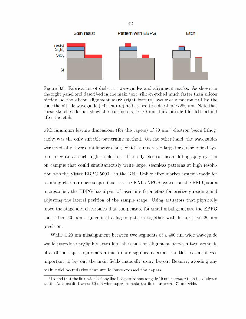
42
Figure 3.8: Fabrication of dielectric waveguides and alignment marks. As shown inthe right panel and described in the main text, silicon etched much faster than siliconnitride, so the silicon alignment mark (right feature) was over a micron tall by thetime the nitride waveguide (left feature) had etched to a depth of ∼260 nm. Note thatthese sketches do not show the continuous, 10-20 nm thick nitride film left behindafter the etch.
with minimum feature dimensions (for the tapers) of 80 nm,3 electron-beam lithog-
raphy was the only suitable patterning method. On the other hand, the waveguides
were typically several millimeters long, which is much too large for a single-field sys-
tem to write at such high resolution. The only electron-beam lithography system
on campus that could simultaneously write large, seamless patterns at high resolu-
tion was the Vistec EBPG 5000+ in the KNI. Unlike after-market systems made for
scanning electron microscopes (such as the KNI’s NPGS system on the FEI Quanta
microscope), the EBPG has a pair of laser interferometers for precisely reading and
adjusting the lateral position of the sample stage. Using actuators that physically
move the stage and electronics that compensate for small misalignments, the EBPG
can stitch 500 µm segments of a larger pattern together with better than 20 nm
precision.
While a 20 nm misalignment between two segments of a 400 nm wide waveguide
would introduce negligible extra loss, the same misalignment between two segments
of a 70 nm taper represents a much more significant error. For this reason, it was
important to lay out the main fields manually using Layout Beamer, avoiding any
main field boundaries that would have crossed the tapers.
3I found that the final width of any line I patterned was roughly 10 nm narrower than the designedwidth. As a result, I wrote 80 nm wide tapers to make the final structures 70 nm wide.
43
Working with ma-N 2403 negative-tone electron-beam resist introduced additional
considerations. The resist had to be thick enough not to completely degrade during
the plasma etch, but not so thick that the tapered ends, only 70-80 nm wide, would
fall over. Choosing the thickness to be 300 nm ensured that the resist held up during
the etch and that very few tapers fell, but reducing the thickness below 250 nm or
the taper width below 60 nm consistently caused problems. Moreover, I found that
cleaning the chip with piranha solution, etching it briefly in buffered HF to remove the
surface oxynitride, and pre-baking it before spinning the resist noticeably improved
the adhesion between the resist and the chip.
Having made these considerations for the layout of the waveguide pattern and the
preparation of the resist, writing the waveguides was straightforward. The patterns
I wrote were relatively sparse, so it was not necessary to correct for the proximity
effect [59]. I found that it was helpful to reduce the relative dose of larger features
like alignment marks, though, to avoid overexposing them. The alignment marks in
the dicing pattern were usually of poor quality, but the EBPG was always eventually
able to locate them anyway. The alignment between these two layers did not have to
be precise, so better marks were not needed. To reduce the amount of time required
for finding the marks, I typically only specified one mark per die.
In contrast, subsequent layers had to be aligned very precisely with the nitride
waveguides. To this end, I included a set of high-quality etched marks in the waveg-
uide pattern. I placed these marks on the exposed silicon in the corners of each die
(see the dicing pattern in Figure 3.7). The etch I used etches silicon about five times
faster than silicon nitride, so by the time I had etched ∼260 nm into the nitride to
define the waveguides, the alignment marks were well over a micron tall (see Fig-
ure 3.8). At this height, and with crisp edges and vertical sidewalls, these marks
provided excellent, high-contrast references for subsequent aligned lithography steps.
The importance of good alignment marks for subsequent processing steps cannot
be overstated. I found that the sharpest, highest-contrast marks I could make were
patterned either by depositing and lifting-off gold or by etching silicon to a depth of at
least one micron using a vertical plasma etch. On marks with sloping sidewalls or low

44
contrast (e.g., Al, SiO2, SiNx, even Ti and Cr), I would often measure uncertainties
in the edge positions of hundreds of nanometers,4 whereas with better marks these
uncertainties were typically a couple of tens of nanometers. To position the recessed
gold pads for the DLSPPWs to within 50 nm of the dielectric waveguides, for example,
good alignment marks were crucial.
After patterning the waveguides in resist using the EBPG, I transferred the pat-
tern into the silicon nitride layer using a mixed-mode “pseudo-Bosch” plasma etch
[60]. This etch involved a mixture of sulfur hexafluoride (SF6) and octafluorocyclobu-
tane (C4F8), which simultaneously etched the horizontal surfaces and passivated the
vertical surfaces, respectively. During the etch, the strained C4F8 molecules opened
and polymerized, forming a protective layer of fluorinated polymer that inhibited
chemical etching. Incoming ions that had been directed perpendicular to the sample
sputtered this layer away from horizontal surfaces, though, exposing them to chemical
attack by fluoride ions and fluorine radicals, the dissociation products of SF6. Vertical
surfaces remained passivated, in contrast, preventing lateral etching. The result was
a nearly vertical etch, whose profile and etch rate could be controlled by adjusting,
among other parameters, the ratio of C4F8 to SF6.
To obtain a dense plasma—and hence a reasonable etch rate—without causing too
much damage to the resist, I used an etcher (Oxford ICP 380) with an inductively
coupled plasma (ICP) source. This tool has two separate radio frequency (RF) cir-
cuits: a vertically-oriented traditional reactive ion etch (RIE) circuit (the “forward”
circuit) capable of operating at up to several hundred watts, and an ICP circuit capa-
ble of handling up to several kilowatts. In typical etches (see the Appendix), I applied
∼1000 W to the ICP circuit to dissociate the etch gases and form a dense plasma,
but only 20-25 W to the forward circuit to direct ions into the sample. Because the
ICP coil was parallel to the plane of the sample being etched, applying a large power
to it did not cause aggressive sputtering of the sample.
Although this approach certainly improved the selectivity of this etch compared
4For details about how to make this measurement, see the entry for the command “measuremarker properties” in the EBPG manual.
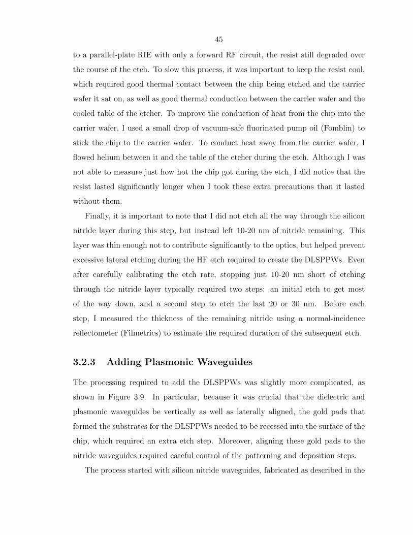
45
to a parallel-plate RIE with only a forward RF circuit, the resist still degraded over
the course of the etch. To slow this process, it was important to keep the resist cool,
which required good thermal contact between the chip being etched and the carrier
wafer it sat on, as well as good thermal conduction between the carrier wafer and the
cooled table of the etcher. To improve the conduction of heat from the chip into the
carrier wafer, I used a small drop of vacuum-safe fluorinated pump oil (Fomblin) to
stick the chip to the carrier wafer. To conduct heat away from the carrier wafer, I
flowed helium between it and the table of the etcher during the etch. Although I was
not able to measure just how hot the chip got during the etch, I did notice that the
resist lasted significantly longer when I took these extra precautions than it lasted
without them.
Finally, it is important to note that I did not etch all the way through the silicon
nitride layer during this step, but instead left 10-20 nm of nitride remaining. This
layer was thin enough not to contribute significantly to the optics, but helped prevent
excessive lateral etching during the HF etch required to create the DLSPPWs. Even
after carefully calibrating the etch rate, stopping just 10-20 nm short of etching
through the nitride layer typically required two steps: an initial etch to get most
of the way down, and a second step to etch the last 20 or 30 nm. Before each
step, I measured the thickness of the remaining nitride using a normal-incidence
reflectometer (Filmetrics) to estimate the required duration of the subsequent etch.
3.2.3 Adding Plasmonic Waveguides
The processing required to add the DLSPPWs was slightly more complicated, as
shown in Figure 3.9. In particular, because it was crucial that the dielectric and
plasmonic waveguides be vertically as well as laterally aligned, the gold pads that
formed the substrates for the DLSPPWs needed to be recessed into the surface of the
chip, which required an extra etch step. Moreover, aligning these gold pads to the
nitride waveguides required careful control of the patterning and deposition steps.
The process started with silicon nitride waveguides, fabricated as described in the
46
Figure 3.9: Fabrication of DLSPPWs. These sketches represent a cross-section of thechip along the axis of the dielectric and plasmonic waveguides (all collinear in thisexample). Note that the pattern defining the PMMA stripe in the final panel is notvisible from this perspective.
previous section, that I had deliberately designed with a 10-20 µm segment missing.
As shown in the first panel of Figure 3.9, I first wrote a rectangle of the same length
directly over the missing segment, forming a window in the PMMA resist. After a
brief xenon difluoride etch (not shown) to remove the remaining silicon nitride in the
patterned area, I used hydrofluoric acid to etch ∼150 nm into the underlying SiO2.
I then deposited a layer of gold of precisely the same thickness as the depth of the
etch, filling the etched hole so that the top surface of the gold was flush with the
bottom surface of the nitride waveguides. A final lithography step defined a stripe in
the PMMA across the gold pad, forming the dielectric load of the DLSPPW.
Aligning the recessed gold pads to the nitride waveguides required some fine-tuning
of this process. In particular, although the EBPG can align two patterns to within a
few tens of nanometers (if the alignment marks are of sufficiently high quality), in this
case I needed to shrink the gold pads by 100 nm on each end in order to guarantee
that they did not overlap the ends of the nitride waveguides. It appeared that this
extra precaution was necessary both because the lithography, etching, and deposition
steps created a slightly larger gold pad than had been written, and also because
47
systematic variations in the positioning of the gold pad were sometimes large enough
to cause the pad to cover the nitride waveguides. These variations were typically the
same on each of the nine dice on a chip, despite the fact that each die had its own
set of alignment marks. As a result, I concluded that the alignment marks were not
responsible for the positioning error.
In fracturing the patterns that contained these gold pads, I used the Proximity
Effect Correction module in Layout Beamer. This step reduced the dose delivered to
the interiors of the pads and increased the dose around their perimeters, compensating
the proximity effect and ensuring that the entire pattern received a roughly equal
dose. More information about the proximity effect in electron-beam lithography can
be found in ref. [59].
Of the three e-beam evaporators available in the KNI, the Lesker gave the best
gold films by far. There were two main reasons for this: the crucible holding the gold
was smaller in this system than in the others, and it was also farther away from the
sample. As a result, the molten gold more closely approximated a true point source,
and the distribution of angles at which gold adatoms impinged on the surface was
correspondingly narrower, peaked sharply around 90◦. Deposition onto the sidewalls
of the resist was therefore less than in the other systems, and the resulting gold pads
therefore had sharper edges and flatter surfaces.
Another issue with the gold deposition was that the gold source would frequently
spit, regardless of which evaporator was used, resulting in micron-scale spheres of
gold across the surface of the deposited films. Two factors likely contributed to
this problem [61]: a thin layer of carbon covered the top of the melt, inhibiting
evaporation until the gold underneath boiled, causing bubbles to burst through the
film; and the molten gold did not wet the crucible well, so that bubbles formed at the
wall would grow large before dislodging. In both cases, when the bubbles burst they
spewed small droplets of molten gold upwards, only the smallest of which (typically
1-5 µm in diameter) would make it to the sample. Adding flakes of tantalum to the
gold source [61] gettered the carbon and improved the wetting at the crucible wall,
reducing or eliminating the spitting. Interestingly, it was possible to see the effect of
48
the tantalum directly: the carbon film, which appeared brighter under electron-beam
heating due to its higher emissivity, broke up into pieces and migrated to the crucible
wall, leaving a uniform, relatively darker patch of pure molten gold in the center of
the crucible.
One final note about evaporating gold: it does not adhere well to silicon or silicon
dioxide. Even features that are hundreds of microns across tend to peel off of these
substrates. To prevent this from happening during this step, I evaporated a thin
(∼5 nm) layer of titanium before depositing the gold. Titanium adheres strongly to
silicon-based materials, and gold adheres well to titanium. In this particular appli-
cation, having a titanium layer across the back surface of the gold pads also helped
damp any surface plasmon that might have been excited there.
Finally, patterning the PMMA stripes that formed the DLSPPWs actually re-
quired two separate lithography steps. First, I spun a 2.5 µm thick layer of PMMA
for the spot-size converters and patterned a large window to clear the PMMA away
from within ∼250 µm of the plasmonic components. This step was important to
ensure that the thinner layer of PMMA would spin evenly across the areas where the
DLSPPWs would be. In a second step, I spun 350 nm of PMMA and patterned the
DLSPPWs in it. As shown in Figure 3.10, this write simply removed the PMMA
from next to the DLSPPW, about one micron on either side, leaving a 350 nm stripe
of PMMA behind. With such small areas being written, it was not necessary to cor-
rect for the proximity effect. I did fracture the pattern at high (2.5 nm) resolution
and write it with a small (1 nA) beam, though, to capture as much detail as possi-
ble. With good alignment marks, I could typically align this pattern to the nitride
waveguides to within about 50 nm.
3.2.4 Dicing a Finished Chip
Having fabricated the main components of the chip as described in the previous
sections, the final remaining challenge was to dice the chip. This task turned out to
be surprisingly difficult. Even with the dicing pattern described in Section 3.1.5, it

49
Figure 3.10: Scanning electron microscope image of a completed DLSPPW.
was still necessary to optimize the dicing process to improve the yield.
The key to solving this problem turned out to be remarkably simple. Figure 3.11
shows a sketch of a chip during cleaving. The chip would have been scribed at
either position A or B and would sit atop a glass slide, the edge of the slide directly
underneath the scribe and the right edge of the chip hanging off the slide. Holding the
left edge of the chip fixed and pressing down on the position marked with an X would
cause the chip to strain, as indicated by the black bend contours, and eventually
to cleave. If the scribe mark had been made at position A, there is a good chance
the chip would cleave in a straight line, since the bend contours there are relatively
straight. In contrast, trying to scribe and cleave it at position B would likely result
in a crooked or curved cleave, since the strain there is less uniform.
The longer the lever arm used for cleaving, then, the better the chances of ob-
taining a straight, clean break. In practice, I accomplished this goal by changing the
order in which I made the cleaves. One advantage of this solution was that I did not
have to make the chips any larger or the dice on them any smaller than they already
were. For a diagram and detailed description of this process, please see the Appendix.
Figure 3.12 shows scanning electron microscope images of a finished chip. The
small, light-colored rectangle in the center panel is the recessed gold pad, on top of
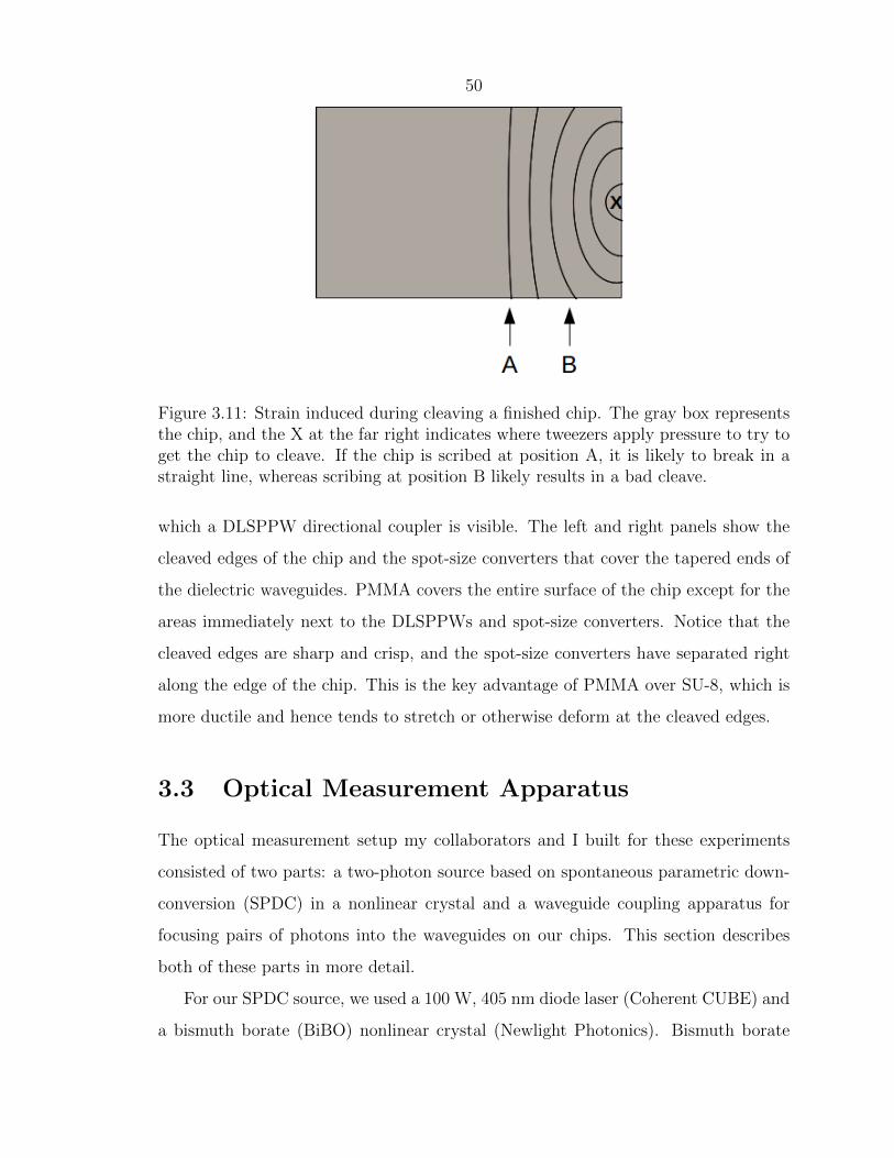
50
Figure 3.11: Strain induced during cleaving a finished chip. The gray box representsthe chip, and the X at the far right indicates where tweezers apply pressure to try toget the chip to cleave. If the chip is scribed at position A, it is likely to break in astraight line, whereas scribing at position B likely results in a bad cleave.
which a DLSPPW directional coupler is visible. The left and right panels show the
cleaved edges of the chip and the spot-size converters that cover the tapered ends of
the dielectric waveguides. PMMA covers the entire surface of the chip except for the
areas immediately next to the DLSPPWs and spot-size converters. Notice that the
cleaved edges are sharp and crisp, and the spot-size converters have separated right
along the edge of the chip. This is the key advantage of PMMA over SU-8, which is
more ductile and hence tends to stretch or otherwise deform at the cleaved edges.
3.3 Optical Measurement Apparatus
The optical measurement setup my collaborators and I built for these experiments
consisted of two parts: a two-photon source based on spontaneous parametric down-
conversion (SPDC) in a nonlinear crystal and a waveguide coupling apparatus for
focusing pairs of photons into the waveguides on our chips. This section describes
both of these parts in more detail.
For our SPDC source, we used a 100 W, 405 nm diode laser (Coherent CUBE) and
a bismuth borate (BiBO) nonlinear crystal (Newlight Photonics). Bismuth borate

51
Figure 3.12: Scanning electron microscope images of a finished chip. The left and rightpanels show the end facets of the chip, where 2.5 µm spot-size converters covered thetapered ends of the waveguides. The center panel shows a 50-50 directional couplerformed out of DLSPPWs with silicon nitride waveguides at the inputs and outputs.
is an excellent nonlinear optical material for this application: it has an effective
nonlinear coefficient 1.5-2 times larger than that of barium borate (BBO), the main
alternative, and unlike BBO does not need to be kept in a dry environment. This
latter point was particularly important for our experiments because it meant that
the crystal did not need to be reinserted into its mount and realigned every time we
used it.
Figure 3.13 shows our SPDC source. The main components are labeled, including
the diode laser at the top of the image and the BiBO crystal towards the bottom
left. To increase the number of pairs of photons this setup produced, we used the
lenses labeled “focusing lens” and “collection lenses” to focus the laser into the crystal
and collect the divergent down-converted light. All three lenses were positioned one
focal-length from the crystal. The collimators in the bottom right corner collected
the down-converted photons into a pair of polarization-maintaining fibers, not shown.
Just in front of each collimator was a 5 nm bandpass filter centered at 814 nm to
reject stray 405 nm light and other background light.
To align this setup, we would usually remove the lenses and connect the fibers from
the collimators directly to our single-photon detectors (PicoQuant τ -SPADs). After
adjusting the phase-matching angle and one of the collimators for maximum signal
at the corresponding detector, we would align the other collimator to maximize the
coincidence count rate. We would then insert the lenses, first aligning the focusing
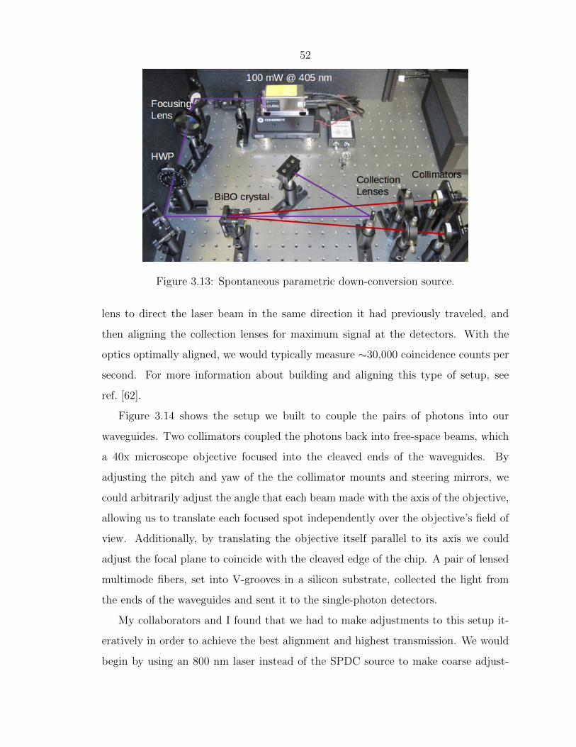
52
Figure 3.13: Spontaneous parametric down-conversion source.
lens to direct the laser beam in the same direction it had previously traveled, and
then aligning the collection lenses for maximum signal at the detectors. With the
optics optimally aligned, we would typically measure ∼30,000 coincidence counts per
second. For more information about building and aligning this type of setup, see
ref. [62].
Figure 3.14 shows the setup we built to couple the pairs of photons into our
waveguides. Two collimators coupled the photons back into free-space beams, which
a 40x microscope objective focused into the cleaved ends of the waveguides. By
adjusting the pitch and yaw of the the collimator mounts and steering mirrors, we
could arbitrarily adjust the angle that each beam made with the axis of the objective,
allowing us to translate each focused spot independently over the objective’s field of
view. Additionally, by translating the objective itself parallel to its axis we could
adjust the focal plane to coincide with the cleaved edge of the chip. A pair of lensed
multimode fibers, set into V-grooves in a silicon substrate, collected the light from
the ends of the waveguides and sent it to the single-photon detectors.
My collaborators and I found that we had to make adjustments to this setup it-
eratively in order to achieve the best alignment and highest transmission. We would
begin by using an 800 nm laser instead of the SPDC source to make coarse adjust-

53
Figure 3.14: Waveguide coupling apparatus.
ments, removing the fiber array holder from the output side of the waveguides and
collecting the divergent light using a camera pointed at the edge of the chip (not
shown). When an input beam was aligned precisely with a waveguide, the image
formed at the camera would show a small, bright spot with several diffraction rings
around it. Minor adjustments to the focus, collimator, and steering mirror would
make this spot brighter or dimmer. Aligning both optical paths this way, we would
then replace the fiber array holder at the output side and align it by connecting one of
the output fibers to a power meter. After making several more rounds of adjustments
to the collimators, steering mirrors, and focus, we would replace the alignment laser
with the fibers from the SPDC source, connect the output multimode fibers to the
single-photon detectors, and make final adjustments to the collimators.
Throughout the entire process, we would take care to keep the axis of the micro-
scope objective centered between the two waveguides. This way, neither input beam
was focused to the far edge of the objective’s field of view, where it would risk being
partially blocked.
With optimal alignment, we typically measured around 35% transmission through

54
a single defect-free dielectric waveguide, though sometimes we measured better than
40% transmission. This value included losses from coupling into and out of the
waveguide and propagation through the waveguide, as well as losses at the collimator
and microscope objective. Isolating the in- and out-coupling losses from reflections
at the collimator and objective was difficult, but we were able to establish an upper
bound on the total coupling loss of about 50%.
55
Chapter 4
Two-Plasmon QuantumInterference
The first experiment my collaborators and I performed involved measuring quantum
interference in a plasmonic 50-50 directional coupler. This chapter describes this ex-
periment, beginning with some motivating remarks and a generalization of the theory
of TPQI to the case of a lossy directional coupler. I then describe our experimental
methods and results before concluding with some thoughts about future work.
4.1 Motivation
As described in Section 2.3, two-photon quantum interference only occurs when the
two input photons are indistinguishable.1 A measurement of high-visibility TPQI
between plasmons therefore shows that initially identical photons remain indistin-
guishable after they are converted to plasmons. Moreover, the standard scheme for
measuring TPQI (see Figure 4.2 and the accompanying explanation) also provides
information about the mutual coherence of the two photons involved. Such a mea-
surement for plasmons, then, confirms that they do not lose coherence compared
to the photons that created them, implying that no extra dephasing occurs in the
1More precisely, TPQI occurs when the probability amplitude corresponding to the case whereboth photons are transmitted exactly cancels that in which both are reflected. In our experiment andmost others, this condition is equivalent to the requirement that the photons be indistinguishable.For a (necessarily) more complicated experiment showing TPQI between distinguishable photons,see ref. [63].
56
plasmonic case.
As described in Section 2.2.3, several other groups have performed experiments
aimed at testing the analogy between the photon and the surface plasmon. These in-
volved, for example, verifying that surface plasmons excited by single-photon sources
exhibit single-particle statistics [32, 33, 34, 35]. While these experiments certainly
demonstrated that surface plasmons exist and preserve the single-photon statistics of
the photons that excite them, they do not settle all questions related to two-particle
phenomena like TPQI. For example, a single surface plasmon whose phase has been
scrambled by electron-phonon interactions would look identical in measurements like
these to one that is perfectly coherent. In contrast, TPQI should be able to distinguish
between these cases in principle.
Measurements of polarization [36] and frequency [38, 39] entanglement in plas-
monic systems have shed a bit more light on these questions, again confirming that
surface plasmons behave similarly to photons. Even so, it is not clear that these
experiments provided all the same information contained in a TPQI measurement,
especially considering that they involved only plasmonic hole arrays [36, 38] or low-
loss long range surface plasmon polariton (LRSPP) waveguides [39] rather than the
high-confinement, lossy plasmonic waveguides investigated in this work.
Evidently, my collaborators and I were not the only ones who shared this per-
spective. Several months before we published our measurements of plasmonic TPQI,
Heeres et al. published similar measurements using metallic stripe waveguides [64].
Unfortunately, though, their waveguides supported a second, undesired mode that
they could not avoid exciting given their experimental apparatus. Only the photons
that coupled into the desired mode could couple to the other waveguide at the di-
rectional coupler, so only those contributed to the TPQI signal. As a result, the
authors measured TPQI with a visibility of only 43±2%. Although their calculations
suggested that this reduction in visibility could be attributed entirely to the second
mode of their waveguides, it would have been difficult to experimentally prove this
point. As a result, there was no way to rule out a modest reduction in the visibility
of plasmonic TPQI due to more fundamental causes.

57
Similarly, recent experiments with plasmonic thin-film structures [65, 66] and
weakly-confined long-range surface plasmons [67] suggest that conversion to and from
a plasmonic mode does not necessarily render a photon distinguishable from an ini-
tially indistinguishable partner. Nevertheless, small reductions in the visibility of
TPQI did occur and were attributed to distortions of the single-photon wavepackets
[65] and unbalanced dispersion [67]. Our measurements avoid these issues and provide
definitive evidence of plasmonic quantum interference.
Finally, it is worth mentioning that several other groups had been performing sim-
ilar experiments independently and published their results shortly after we published
ours. The details can be found in refs. [68] and [69].
4.2 TPQI in a Lossy Directional Coupler
The theory of two-photon quantum interference described in Section 2.3 implicitly
assumes that the beam splitter is lossless. In contrast, losses in most plasmonic
structures are typically substantial, including in the directional couplers we studied.
This section develops the theory of TPQI in a lossy directional coupler, starting from
an established result for a lossy free-space beam splitter. It turns out that losses can
reduce the visibility of TPQI in a directional coupler just as in a free-space beam
splitter, albeit by a slightly different mechanism, but in our experiments we calculate
that this effect is negligible.
Following Barnett et al. [70], we start with the probability of detecting one photon
in each output of a lossy, symmetric beam splitter in a Hong-Ou-Mandel measure-
ment,
P (1a, 1b) = |t|4 + |r|4 + (t2r∗2 + t∗2r2)I , (4.1)
where “a” and “b” label the two outputs of the splitter, t and r are the complex
transmission and reflection coefficients that characterize it, and I is a quantity be-
tween zero and one that describes the overlap of the photons at the splitter. In this
notation, |t|2 and |r|2 are the fractions of power transmitted and reflected at the
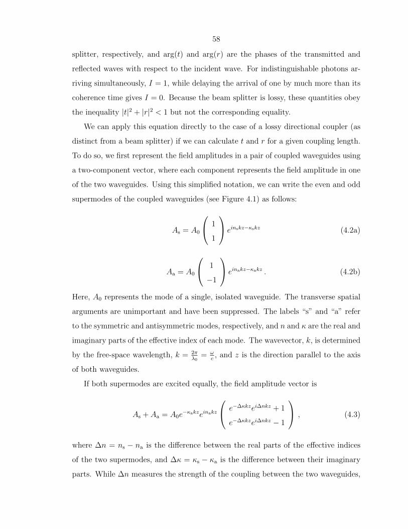
58
splitter, respectively, and arg(t) and arg(r) are the phases of the transmitted and
reflected waves with respect to the incident wave. For indistinguishable photons ar-
riving simultaneously, I = 1, while delaying the arrival of one by much more than its
coherence time gives I = 0. Because the beam splitter is lossy, these quantities obey
the inequality |t|2 + |r|2 < 1 but not the corresponding equality.
We can apply this equation directly to the case of a lossy directional coupler (as
distinct from a beam splitter) if we can calculate t and r for a given coupling length.
To do so, we first represent the field amplitudes in a pair of coupled waveguides using
a two-component vector, where each component represents the field amplitude in one
of the two waveguides. Using this simplified notation, we can write the even and odd
supermodes of the coupled waveguides (see Figure 4.1) as follows:
As = A0
1
1
einskz−κskz (4.2a)
Aa = A0
1
−1
einakz−κakz . (4.2b)
Here, A0 represents the mode of a single, isolated waveguide. The transverse spatial
arguments are unimportant and have been suppressed. The labels “s” and “a” refer
to the symmetric and antisymmetric modes, respectively, and n and κ are the real and
imaginary parts of the effective index of each mode. The wavevector, k, is determined
by the free-space wavelength, k = 2πλ0
= ωc, and z is the direction parallel to the axis
of both waveguides.
If both supermodes are excited equally, the field amplitude vector is
As + Aa = A0e−κakzeinakz
e−∆κkzei∆nkz + 1
e−∆κkzei∆nkz − 1
, (4.3)
where ∆n = ns − na is the difference between the real parts of the effective indices
of the two supermodes, and ∆κ = κs − κa is the difference between their imaginary
parts. While ∆n measures the strength of the coupling between the two waveguides,
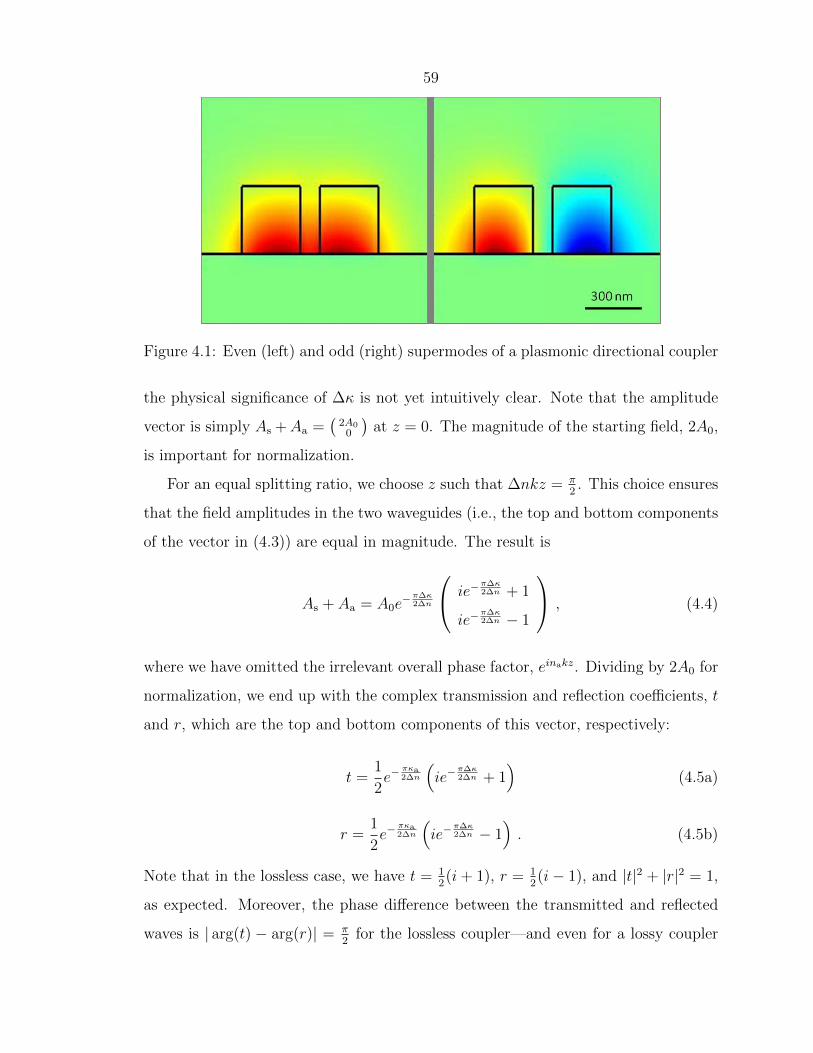
59
Figure 4.1: Even (left) and odd (right) supermodes of a plasmonic directional coupler
the physical significance of ∆κ is not yet intuitively clear. Note that the amplitude
vector is simply As +Aa =(
2A00
)at z = 0. The magnitude of the starting field, 2A0,
is important for normalization.
For an equal splitting ratio, we choose z such that ∆nkz = π2. This choice ensures
that the field amplitudes in the two waveguides (i.e., the top and bottom components
of the vector in (4.3)) are equal in magnitude. The result is
As + Aa = A0e−π∆κ
2∆n
ie−π∆κ2∆n + 1
ie−π∆κ2∆n − 1
, (4.4)
where we have omitted the irrelevant overall phase factor, einakz. Dividing by 2A0 for
normalization, we end up with the complex transmission and reflection coefficients, t
and r, which are the top and bottom components of this vector, respectively:
t =1
2e−
πκa2∆n
(ie−
π∆κ2∆n + 1
)(4.5a)
r =1
2e−
πκa2∆n
(ie−
π∆κ2∆n − 1
). (4.5b)
Note that in the lossless case, we have t = 12(i+ 1), r = 1
2(i− 1), and |t|2 + |r|2 = 1,
as expected. Moreover, the phase difference between the transmitted and reflected
waves is | arg(t) − arg(r)| = π2
for the lossless coupler—and even for a lossy coupler
60
with ∆κ = 0—which is necessary for perfect TPQI (see Section 2.3). In contrast, a
lossy coupler with ∆κ 6= 0 will impart a different relative phase to the two waves,
resulting in the reduced visibility of TPQI.
To make these last observations quantitative, we substitute (4.5a) and (4.5b) into
(4.1). Writing α = |t| = |r| = 12e−
πκa2∆n
(1 + e−
π∆κ∆n
) 12
for the magnitude of t and r and
∆θ = 2 tan−1(eπ∆κ2∆n
)for the phase difference between them, with r = tei∆θ, we have
P (1a, 1b) = 2α4 + 2α4(2 cos2 ∆θ − 1)I . (4.6)
The theoretical maximum visibility of TPQI is then
V = 1− P (1a, 1b; I = 1)
P (1a, 1b; I = 0)= 1− 2 cos2 ∆θ . (4.7)
This expression confirms that a lossy directional coupler with ∆κ 6= 0, and therefore
∆θ 6= π2, cannot give perfect visibility of TPQI.
Fortunately for our experiment, ∆κ in our DLSPPW couplers was small relative
to ∆n, so this effect was negligible. Using a commercial finite-difference frequency-
domain mode solver, we calculated ∆n = 0.129, ∆κ = −4.41× 10⁻⁴, and α = 0.661,
giving a maximum visibility of 0.999.
4.3 Experimental Setup
Figure 4.2 shows a diagram of our experiment. The left half shows the spontaneous
parametric down-conversion (SPDC) source and the right half represents the waveg-
uide coupling setup, both described in detail in Section 3.3. The black lines joining
these two halves represent polarization maintaining fibers, one of which has an ad-
justable optical delay integrated into it.
An optical microscope image of one of the chips we tested for this measurement
is shown in Figure 4.3. The chip had a dielectric 50-50 directional coupler (topmost)
and several plasmonic directional couplers of different coupling lengths, one of which
is shown in Figure 4.4. The light-colored rectangle in the center of the image is
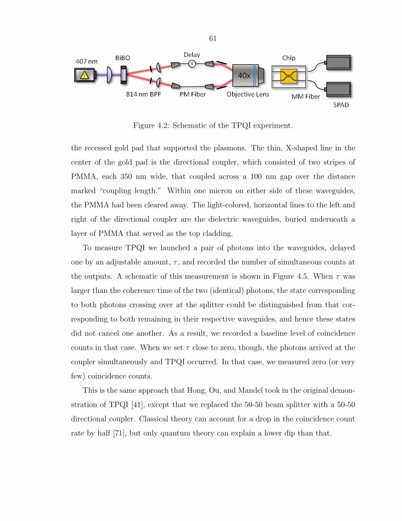
61
Figure 4.2: Schematic of the TPQI experiment.
the recessed gold pad that supported the plasmons. The thin, X-shaped line in the
center of the gold pad is the directional coupler, which consisted of two stripes of
PMMA, each 350 nm wide, that coupled across a 100 nm gap over the distance
marked “coupling length.” Within one micron on either side of these waveguides,
the PMMA had been cleared away. The light-colored, horizontal lines to the left and
right of the directional coupler are the dielectric waveguides, buried underneath a
layer of PMMA that served as the top cladding.
To measure TPQI we launched a pair of photons into the waveguides, delayed
one by an adjustable amount, τ , and recorded the number of simultaneous counts at
the outputs. A schematic of this measurement is shown in Figure 4.5. When τ was
larger than the coherence time of the two (identical) photons, the state corresponding
to both photons crossing over at the splitter could be distinguished from that cor-
responding to both remaining in their respective waveguides, and hence these states
did not cancel one another. As a result, we recorded a baseline level of coincidence
counts in that case. When we set τ close to zero, though, the photons arrived at the
coupler simultaneously and TPQI occurred. In that case, we measured zero (or very
few) coincidence counts.
This is the same approach that Hong, Ou, and Mandel took in the original demon-
stration of TPQI [41], except that we replaced the 50-50 beam splitter with a 50-50
directional coupler. Classical theory can account for a drop in the coincidence count
rate by half [71], but only quantum theory can explain a lower dip than that.
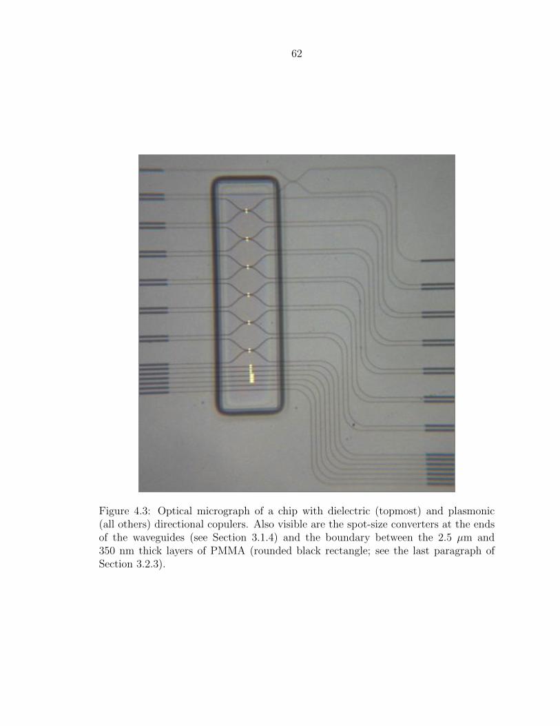
62
Figure 4.3: Optical micrograph of a chip with dielectric (topmost) and plasmonic(all others) directional copulers. Also visible are the spot-size converters at the endsof the waveguides (see Section 3.1.4) and the boundary between the 2.5 µm and350 nm thick layers of PMMA (rounded black rectangle; see the last paragraph ofSection 3.2.3).
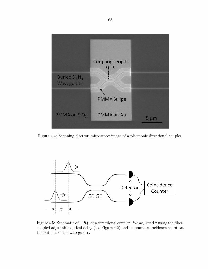
63
Figure 4.4: Scanning electron microscope image of a plasmonic directional coupler.
Figure 4.5: Schematic of TPQI at a directional coupler. We adjusted τ using the fiber-coupled adjustable optical delay (see Figure 4.2) and measured coincidence counts atthe outputs of the waveguides.

64
Figure 4.6: Raw measurements of TPQI in dielectric (left) and plasmonic (right)couplers. The straight lines are linear fits to the background, which decayed overtime as the optics drifted out of alignment.
4.4 Measurements
Figure 4.6 shows our raw measurements in dielectric (left) and plasmonic (right) 50-50
directional couplers. In the case of the dielectric coupler, each point represents the
mean of five measurements while the error bars indicate one standard deviation above
and below the mean. For the plasmonic coupler, these symbols designate the mean
and standard deviation of three measurements. The clear dip in the coincidence
count rate at τ = 0 indicates that the detectors rarely clicked simultaneously, the
experimental signature of TPQI.
The solid lines in these plots show linear fits to the background, which reduced over
time as the optics drifted out of alignment. The measurement using the plasmonic
coupler took approximately five hours, so the drift is more severe than in the dielectric
case, which took roughly 20 minutes to measure. To make for a clearer comparison
between dielectric and plasmonic TPQI, we divided the raw data by the linear fits to
the background, obtaining the normalized plots shown in Figure 4.7.
The red lines represent fits to inverted Gaussian functions, from which we ex-
tracted the visibility of TPQI (the depth of the dip) and the coherence time (the
width of the dip) in each case. More precisely, we defined the visibility as V = 1−Cmin
and the width of the dip as the standard deviation of the Gaussian fit. With these

65
Figure 4.7: Normalized measurements of TPQI in dielectric (left) and plasmonic(right) couplers. The data are the same as in Figure 4.6.
definitions, we obtained visibilities of 0.944 ± 0.003 and 0.932 ± 0.01 in the di-
electric and plasmonic measurements, respectively, identical to within experimental
error. Likewise, we obtained respective widths of 0.12 ± 0.01 ps and 0.11 ± 0.01 ps,
again the same to within experimental error.
A couple of technical details are worth clarifying. First, because the bandwidth of
the down-converted beams (5 nm, set by the filters) was much larger than the band-
width of the pump laser (< 1 nm), the pairs of photons we created were entangled
by frequency, as was also the case in the original paper by Hong, Ou, and Mandel
[41]. There the authors showed that such an input (eq. 3 in their paper) gives pre-
cisely the result that we observed when the filters that determine the spectra of the
down-converted photons are Gaussian, which is a good approximation in the present
measurement.
Unlike the original HOM experiment, however, this experiment used a plasmonic
directional coupler in lieu of a beam splitter. In principle, the splitting ratio of our
coupler and the phase difference between the transmitted and reflected waves both
depended on frequency, and this dependence could have played a role in the theory
of our measurement. If that were so, the frequency correlations between photons
might thereby have become important. Our calculations suggested that this was not
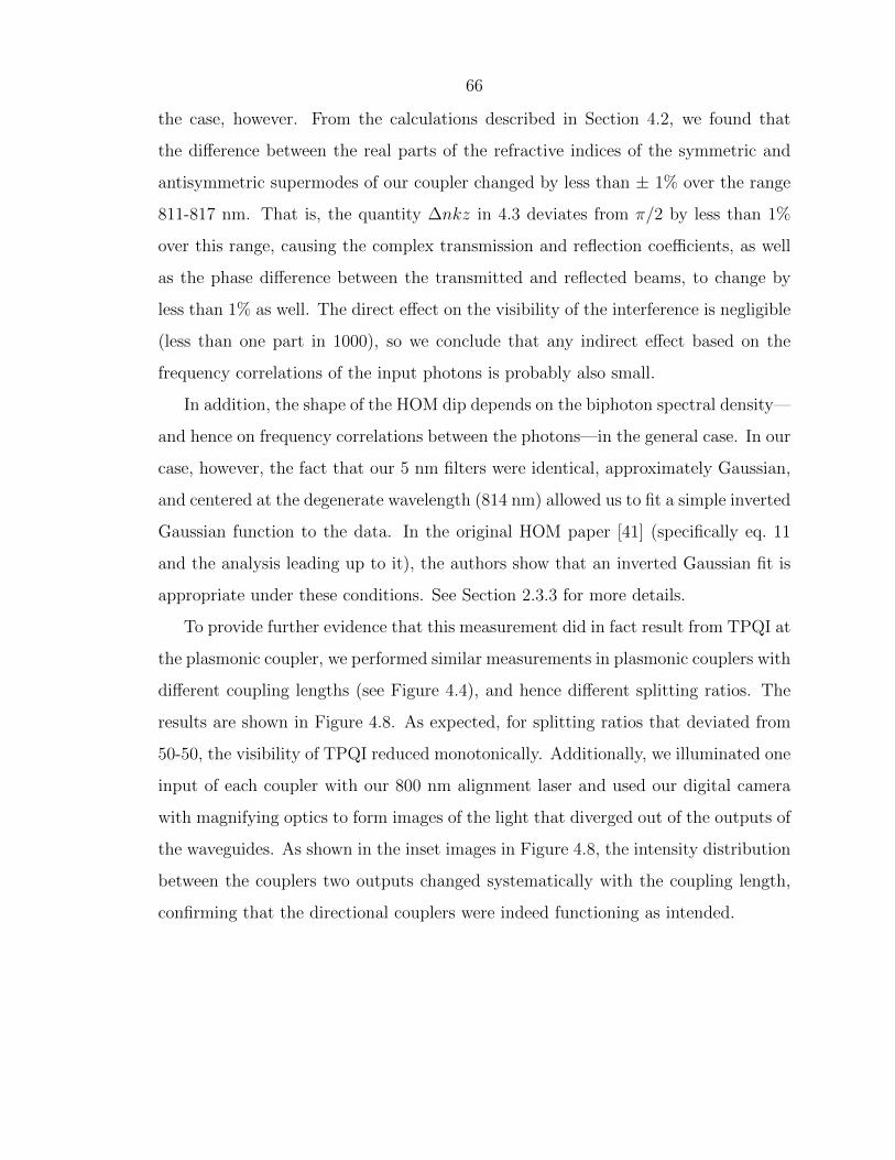
66
the case, however. From the calculations described in Section 4.2, we found that
the difference between the real parts of the refractive indices of the symmetric and
antisymmetric supermodes of our coupler changed by less than ± 1% over the range
811-817 nm. That is, the quantity ∆nkz in 4.3 deviates from π/2 by less than 1%
over this range, causing the complex transmission and reflection coefficients, as well
as the phase difference between the transmitted and reflected beams, to change by
less than 1% as well. The direct effect on the visibility of the interference is negligible
(less than one part in 1000), so we conclude that any indirect effect based on the
frequency correlations of the input photons is probably also small.
In addition, the shape of the HOM dip depends on the biphoton spectral density—
and hence on frequency correlations between the photons—in the general case. In our
case, however, the fact that our 5 nm filters were identical, approximately Gaussian,
and centered at the degenerate wavelength (814 nm) allowed us to fit a simple inverted
Gaussian function to the data. In the original HOM paper [41] (specifically eq. 11
and the analysis leading up to it), the authors show that an inverted Gaussian fit is
appropriate under these conditions. See Section 2.3.3 for more details.
To provide further evidence that this measurement did in fact result from TPQI at
the plasmonic coupler, we performed similar measurements in plasmonic couplers with
different coupling lengths (see Figure 4.4), and hence different splitting ratios. The
results are shown in Figure 4.8. As expected, for splitting ratios that deviated from
50-50, the visibility of TPQI reduced monotonically. Additionally, we illuminated one
input of each coupler with our 800 nm alignment laser and used our digital camera
with magnifying optics to form images of the light that diverged out of the outputs of
the waveguides. As shown in the inset images in Figure 4.8, the intensity distribution
between the couplers two outputs changed systematically with the coupling length,
confirming that the directional couplers were indeed functioning as intended.

67
Figure 4.8: Measurements of TPQI in plasmonic couplers of different coupling lengths.
4.5 Summary and Outlook
From these results, we concluded that our experiment demonstrated unambiguous
quantum interference in plasmonic waveguides. Moreover, the close correspondence
between our measurements of TPQI in dielectric and plasmonic waveguides showed
that identical photons remain indistinguishable from one another even in tightly-
confined, high-loss plasmonic structures in which the electromagnetic fields interact
strongly with the metal. This high degree of coherence confirms that plasmonic com-
ponents could indeed find application in quantum computing if loss can be mitigated.
Finally, by integrating plasmonic waveguides directly into a chip-based quantum pho-
tonics platform operating at room temperature, our experiment laid the groundwork
for further investigations of quantum interference and entanglement in plasmonic cir-
cuits, such as the path entanglement experiment described in the next chapter.

68
Chapter 5
Path-Entanglement of SurfacePlasmons
The second experiment my collaborators and I performed involved preparing path-
entangled states of pairs of photons, converting them to surface plasmons, and verify-
ing that they remained entangled. This chapter describes this experiment, beginning
with a conceptual overview and a brief theoretical explanation of how measurements
of path entanglement can provide information about the presence or absence of deco-
herence. I then describe our experimental methods and the extra fabrication processes
that were necessary to build the chips we studied. Finally, I present our results and
conclude with some thoughts about future work.
5.1 Verifying Entanglement in TPQI
In any TPQI experiment, including the plasmonic version of the measurement de-
scribed in the previous chapter, the resulting state is an entangled one,
|Ψout〉 =1√2
(|2, 0〉+ |0, 2〉) . (5.1)
In such a state, the two photons are entangled by the path they take exiting the
beam splitter. That is, neither photon is known to be in one output or the other
before a measurement is made, but once the output path of one photon is measured
(hypothetically), the other photon is known with certainty to be in the same output.
69
Typical measurements of TPQI, such as the one my collaborators and I made for
surface plasmons, do not actually prove that the output state is the entangled state
of (5.1). They show only that the component |1, 1〉 is absent from the output state.
In particular, a statistical mixture of the states |2, 0〉 and |0, 2〉, each occurring with
50% probability, would give the same experimental result,
|Ψout〉 =
|2, 0〉, P = 0.5
|0, 2〉, P = 0.5. (5.2)
Such a “mixed state” might result from the decoherence of the entangled state in
(5.1), as described in the next section.
How can one experimentally distinguish between the path-entangled state of (5.1)
and the statistical mixture of (5.2)? The trick is to use a second 50-50 beam splitter
(or directional coupler) to produce interference between the two components of the
entangled state. Needless to say, this interference only occurs if both components are
actually present, so no interference occurs if the photons are described by the mixed
state of (5.2).
Figure 5.1 shows how this measurement works in practice. Two 50-50 directional
couplers connected in series form a Mach-Zehnder interferometer, and an adjustable
phase shift is applied in one of the two waveguides between the couplers. Two photons
incident simultaneously from the left enter the first coupler and, as a result of quantum
interference, exit in the entangled state of (5.1). Shifting the phase along one path
rotates the (relative) phase of the corresponding state,
1√2
(|2, 0〉+ |0, 2〉) phase shift−−−−−−−→ |Ψout〉 =1√2
(ei2φ|2, 0〉+ |0, 2〉
). (5.3)
Quantum interference at the second coupler then produces a complicated output state
that depends on φ,
2nd coupler−−−−−−−→1
4
[ei2φ
(√2|2, 0〉 − 2i|1, 1〉 −
√2|0, 2〉
)+(−√
2|2, 0〉 − 2i|1, 1〉+√
2|0, 2〉)]
.
(5.4)
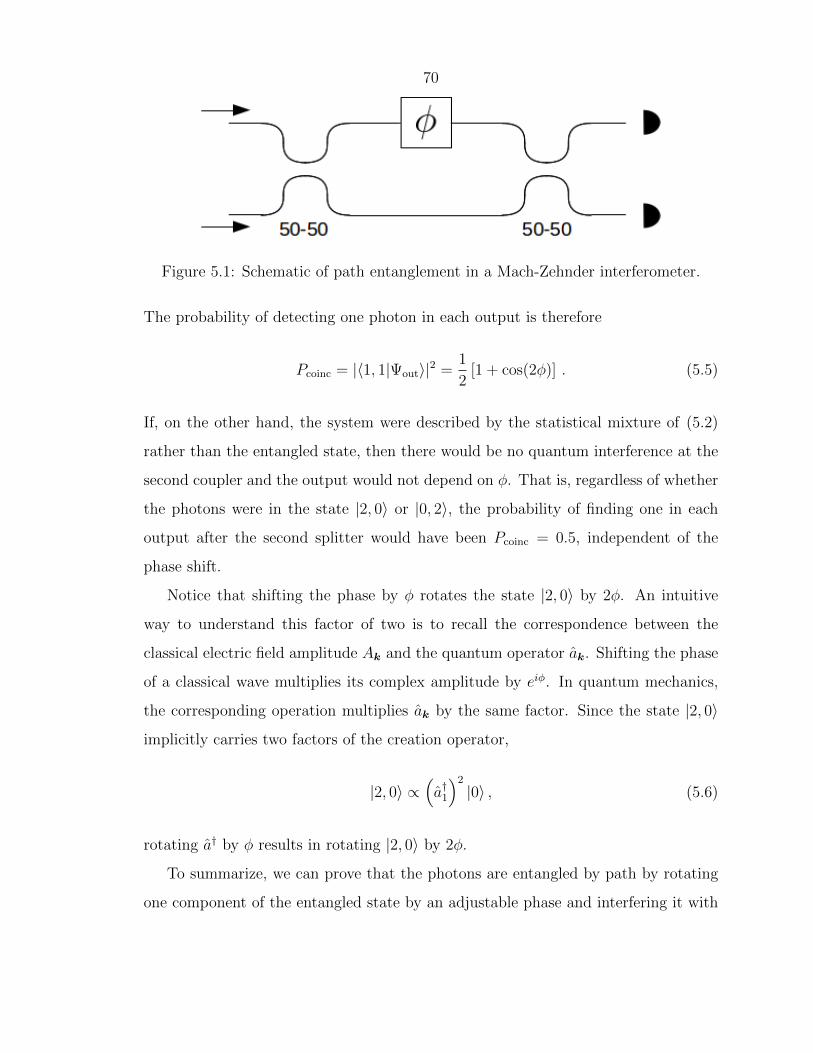
70
Figure 5.1: Schematic of path entanglement in a Mach-Zehnder interferometer.
The probability of detecting one photon in each output is therefore
Pcoinc = |〈1, 1|Ψout〉|2 =1
2[1 + cos(2φ)] . (5.5)
If, on the other hand, the system were described by the statistical mixture of (5.2)
rather than the entangled state, then there would be no quantum interference at the
second coupler and the output would not depend on φ. That is, regardless of whether
the photons were in the state |2, 0〉 or |0, 2〉, the probability of finding one in each
output after the second splitter would have been Pcoinc = 0.5, independent of the
phase shift.
Notice that shifting the phase by φ rotates the state |2, 0〉 by 2φ. An intuitive
way to understand this factor of two is to recall the correspondence between the
classical electric field amplitude Ak and the quantum operator ak. Shifting the phase
of a classical wave multiplies its complex amplitude by eiφ. In quantum mechanics,
the corresponding operation multiplies ak by the same factor. Since the state |2, 0〉
implicitly carries two factors of the creation operator,
|2, 0〉 ∝(a†1
)2
|0〉 , (5.6)
rotating a† by φ results in rotating |2, 0〉 by 2φ.
To summarize, we can prove that the photons are entangled by path by rotating
one component of the entangled state by an adjustable phase and interfering it with

71
the other component at a second 50-50 coupler. The number of coincidence counts1
at the outputs will oscillate sinusoidally with φ if the photons are entangled and will
remain constant if they are instead in a mixed state.
5.2 Using Path Entanglement to Look for Deco-
herence
Decoherence occurs when the environment of a quantum system that is superposed
between two or more states interacts with the system in a way that distinguishes
between the superposed states [6, 7]. For example, a C60 molecule superposed be-
tween several different positions at the same time can exhibit quantum interference
until it scatters from an ambient gas molecule [72]. Each component of the super-
position would cause a different change in the momentum of the gas molecule—or,
more likely, an entirely different scattering event with another gas molecule—so the
gas molecules (constituting the “environment”) collectively store some information
about the superposition. Ignoring their positions and momenta and only measuring
the C60 molecule, it is impossible to recover the superposition state, which now in-
cludes components of the environment as well. Instead, averaging over the different
states of the environment effectively destroys any evidence of quantum interference.
In principle, any interaction between a plasmon and the metal that supports it
could similarly cause decoherence if the plasmon is in a superposition of traveling
two different paths. In particular, if path-entangled plasmons scatter from phonons
or electrons in the metal without being absorbed, thereby leaving behind a record of
their existence in the electronic or atomic motions of the metal, it should be possible
to detect the resulting decoherence as a reduction in the visibility of entanglement.
Experiments to date have shown that photons that are entangled by polariza-
tion [36] or frequency [38, 39] do indeed remain entangled after being converted to
plasmons and back to photons, but ours is the first experiment with path-entangled
1Notice that the count rate in each output separately will be constant with φ. The oscillationoccurs only in the correlation between the two outputs.
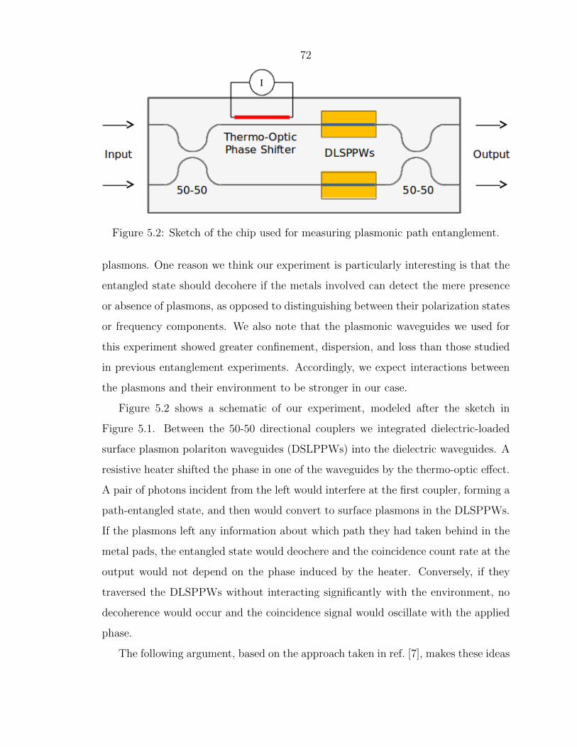
72
Figure 5.2: Sketch of the chip used for measuring plasmonic path entanglement.
plasmons. One reason we think our experiment is particularly interesting is that the
entangled state should decohere if the metals involved can detect the mere presence
or absence of plasmons, as opposed to distinguishing between their polarization states
or frequency components. We also note that the plasmonic waveguides we used for
this experiment showed greater confinement, dispersion, and loss than those studied
in previous entanglement experiments. Accordingly, we expect interactions between
the plasmons and their environment to be stronger in our case.
Figure 5.2 shows a schematic of our experiment, modeled after the sketch in
Figure 5.1. Between the 50-50 directional couplers we integrated dielectric-loaded
surface plasmon polariton waveguides (DSLPPWs) into the dielectric waveguides. A
resistive heater shifted the phase in one of the waveguides by the thermo-optic effect.
A pair of photons incident from the left would interfere at the first coupler, forming a
path-entangled state, and then would convert to surface plasmons in the DLSPPWs.
If the plasmons left any information about which path they had taken behind in the
metal pads, the entangled state would deochere and the coincidence count rate at the
output would not depend on the phase induced by the heater. Conversely, if they
traversed the DLSPPWs without interacting significantly with the environment, no
decoherence would occur and the coincidence signal would oscillate with the applied
phase.
The following argument, based on the approach taken in ref. [7], makes these ideas

73
more precise. Quantum interference at the first coupler produces a path-entangled
state,
|1, 1〉 ⊗ |Ei〉 1st coupler−−−−−−−→1√2
(|2, 0〉+ |0, 2〉)⊗ |Ei〉 , (5.7)
where |i, j〉 denotes a state with i photons in one waveguide and j photons in the other,
and |Ei〉 represents the state of the environment before the photons are converted to
surface plasmons. Here, the “environment” refers to all of the degrees of freedom of
the electrons and phonons in the two metal pads that form the plasmonic waveguides.
(We describe decoherence in this system using a von Neumann model of measurement,
as described in Section III of ref. [6].) The heater introduces a phase shift to only the
component in which both photons are in the first waveguide,
1√2
(|2, 0〉+ |0, 2〉)⊗ |Ei〉 phase shift−−−−−−−→1√2
(ei2φ|2, 0〉+ |0, 2〉
)⊗ |Ei〉 . (5.8)
As described in the previous section, the relative phase φ imparted by the heater
contributes a phase to the state |2, 0〉 which is twice as large.
At the plasmonic waveguides, the state of the environment evolves along with the
state of the plasmons,
1√2
(ei2φ|2, 0〉+ |0, 2〉
)⊗ |Ei〉 plasmons−−−−−−→
1√2
(ei2φ|2, 0〉 ⊗ |E2,0〉+ |0, 2〉 ⊗ |E0,2〉
).
(5.9)
Here, |E2,0〉 is the state of the environment that would result from both plasmons
traversing the first waveguide, and |E0,2〉 is the corresponding state for the other
case. These two states are equal if the plasmons do not interact at all with their
environment, but they would be different in the case that the plasmons elastically
scatter from electrons or phonons, as described earlier. Note also that we have ignored
components of the resulting state that have fewer than two plasmons. Physically,
this corresponds to post-selecting for only those trials in which neither plasmon was
absorbed.
Finally, quantum interference at the second coupler produces a complicated output
74
state:
2nd coupler−−−−−−−→1
4
[ei2φ
(√2|2, 0〉 − 2i|1, 1〉 −
√2|0, 2〉
)⊗ |E2,0〉
+(−√
2|2, 0〉 − 2i|1, 1〉+√
2|0, 2〉)⊗ |E0,2〉
].
(5.10)
Constructing the density operator corresponding to this state and tracing over the
degrees of freedom of the environment gives the reduced density operator of the
surface plasmons, ρred, from which the probability of detecting simultaneous counts
at the outputs can be found:
Pcoinc = 〈1, 1|ρred|1, 1〉 =1
2[1 + |〈E2,0|E0,2〉 cos(2φ)] . (5.11)
In the absence of interactions between the plasmons and the environment, we have
|E2,0〉 = |E0,2〉 and, as a result, Pcoinc = 12[1 + cos(2φ)]. In contrast, if the surface
plasmons alter the state of the metal such that |〈E2,0|E0,2〉| < 1, the amplitude of the
sinusoidal oscillation of Pcoinc is reduced, with the case |〈E2,0|E0,2〉| = 0 corresponding
to total decoherence and no dependence of Pcoinc on φ. In summary, by measuring the
coincidence count rate at the outputs of the waveguides as a function of the applied
phase, φ, we can probe the perseverance or decoherence of the path-entangled plasmon
state.
5.3 Experimental Setup
Figure 5.3 shows the setup of the experiment. The spontaneous parametric down-
conversion source, coupling optics, and detectors are the same ones that we used in
the previous experiment. This time, we set the delay line such that the photons
always arrived simultaneously at the first coupler of the interferometer. Instead of
adjusting the delay setting, we varied the power applied to the heater.
Images of the fabricated chip are shown in Figure 5.4. Panel (a) shows two neigh-
boring interferometers. The thin, black lines are the silicon nitride waveguides, clad
below by SiO2 and above by PMMA. At the far left and right of the image, the 50-50

75
Figure 5.3: Sketch of the plasmonic path entanglement experiment.
directional couplers are visible. The small gold rectangles on the right side of the
image are the gold pads that support the DLSPPWs. The large gold rectangles are
contact pads for the heaters, which are easier to see in panel (b). The large, dark
oval in panels (a) and (b) is an area where we etched the silicon out from underneath
the heaters, as described in Section 5.4.
Panel (b) shows this area more closely. The heaters are the light-colored horizontal
lines that connect the gold contacts. The long, narrow, darker rectangle in the middle
is the hole through which we etched the underlying silicon.
The heaters consisted of strips of a nickel-chromium alloy (80% Ni) that ran
parallel to the waveguides. As shown in panel (d), the distance from the edge of
the heater to the center of the adjacent waveguide was 2.5 µm, large enough for the
heater not to perturb the optical mode of the waveguide but small compared to the
lateral extent of the undercut that isolated the heaters. To reduce the heat capacity
of the isolated structures, we cleared the PMMA cladding away from the undercut
area except for a strip several microns wide that covered the heaters and waveguides,
also shown in panel (d). This change reduced the time required for the optical phase
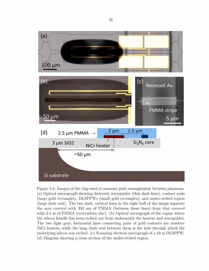
76
Figure 5.4: Images of the chip used to measure path entanglement between plasmons.(a) Optical micrograph showing dielectric waveguides (thin dark lines), contact pads(large gold rectangles), DLSPPWs (small gold rectangles), and under-etched region(large dark oval). The two dark, vertical lines in the right half of the image separatethe area covered with 350 nm of PMMA (between these lines) from that coveredwith 2.5 m of PMMA (everywhere else). (b) Optical micrograph of the region wherethe silicon handle has been etched out from underneath the heaters and waveguides.The two light gray, horizontal lines connecting pairs of gold contacts are resistiveNiCr heaters, while the long, dark oval between them is the hole through which theunderlying silicon was etched. (c) Scanning electron micrograph of a 10 m DLSPPW.(d) Diagram showing a cross section of the under-etched region.

77
shift in the waveguides to reach a steady state from minutes (or tens of minutes) to
seconds.
We used metal probes mounted on micromanipulators to make electrical contact
to the heater contact pads and a Keithley 237 source-measure unit to supply and
measure power. To automate the measurements, we wrote a MATLAB script that
swept the power supplied to the heaters, recording coincidence counts at each setting.
For more information, please see Section 5.5.
5.4 Additional Fabrication Considerations
Fabricating the chip shown in Figure 5.4 presented several additional challenges,
mostly related to isolating the heaters from the substrate. This section provides an
overview of the problems I faced and the solutions I found. For detailed fabrication
instructions, please see the second section of the Appendix.
The first chips I fabricated for this experiment did not have the undercut areas
around the heaters. With only three microns of silicon oxide as insulation, much of
the power supplied to a given heater was conducted into the underlying silicon. In
fact, the substrate would typically get hot enough for thermal expansion to cause the
waveguides to drift out of alignment with the focused input beams. My collaborators
and I were not able to measure the temperature of the chip directly, but we did
observe that the temperature of the metal bock holding the chip would change by
several degrees at the highest settings of the heater power.
To remedy this problem I eventually settled on the design shown in Figure 5.4,
where I removed the silicon from under the heaters. This approach reduced the power
required to achieve a full 2π phase shift by roughly a factor of 50, but it required
significantly more complicated processing.
In particular, etching holes between the waveguides through the nitride and oxide
layers to gain access to the underlying silicon required some special care. I initially
tried to perform this step across an entire 4” wafer, which worked well but caused the
subsequent steps that defined the nitride waveguides to fail. The reason turned out to

78
be subtle: at 3 µm, the holes were deep enough to disrupt the flow of the e-beam resist
in the neighboring areas, resulting in a thinner layer of resist (locally) than intended.
The thinner resist did not survive the plasma etch that transfered the waveguide
pattern into the silicon nitride layer, with the result that the nitride waveguides were
shorter than designed and had rough top surfaces. Consequently, they exhibited
losses which varied from waveguide to waveguide, but which were rarely balanced in
a given interferometer. In addition to reducing the signal in our measurements, these
unbalanced losses also reduced the visibility of classical and quantum interference.
To resolve this issue, I patterned and etched the dielectric waveguides first and
created the holes in the oxide layer afterwards. For the latter etch I used a thick,
positive-tone photoresist (AZ 9245, ∼ 5µm), which I hard-baked to improve its etch
resistance. Before spinning the resist, it was crucial to clean the chip in piranha
solution and then dip it in hydrofluoric acid to strip the native oxynitride. These
steps improved the adhesion of the resist to the nitride, preventing hydrofluoric acid
from undercutting the resist during the subsequent etch. Moreover, for the etch itself
I used buffered HF instead of pure HF, so the reactive species was HF2− instead of
F−. The larger HF2− ions diffused much more slowly through the resist, improving
its etch resistance.
Luckily, these holes did not cause further problems for subsequent lithography
and metal deposition steps. The final definition of the PMMA structures and the
undercut etch required some development, however. I found that the best sequence
for these steps was as follows:
1. Pattern windows in the thick PMMA layer for the DLSPPWs (see Section 3.2.3).
2. Spin the thin PMMA layer and pattern holes in it over the holes in the SiO2.
3. Remove the silicon from underneath the heaters using a XeF2 etch.
4. Pattern the remaining PMMA features, including spot-size converters, DLSP-
PWs, covers for the heaters, and holes over the contact pads.
In particular, step (3) must come after spinning both PMMA layers; otherwise, resist

79
would get into the holes etched into the silicon and would be difficult to remove.
Additionally, I found that step (4) worked best after the XeF2 etch. When I tried to
reverse the order of these two steps, the PMMA covers for the heaters (i.e., directly
above the undercut holes) did not hold up well during the undercut step, possibly
because the PMMA got too hot during the (very exothermic) XeF2 etch.
After completing these steps, I found that I had to handle the chips extremely
carefully to avoid fracturing the thin SiO2 membranes that supported the heaters. In
fact, as can be seen in panel (b) of Figure 5.4, the compressively-strained oxide layer
actually buckled after we removed the silicon from underneath it—notice how the
center of the image is slightly out of focus. These strains undoubtedly caused slight
phase shifts in the waveguides, which explain why the sinusoidal interference signals
we measured (see Figure 5.5) were shifted.
5.5 Measurements
Our measurements consisted of two main steps. First, we set the heater power to
give a phase shift of approximately π/2 and recorded simultaneous counts at the
detectors as a function of the adjustable delay setting. The resulting two-photon
quantum interference (see Figure 4.5 and the surrounding text) allowed us to find
the delay setting that corresponded to the simultaneous arrival of both photons at
the first directional coupler. Second, we stepped the voltage across the heater from
0-3 V (roughly 0-5 mW), recording both one- and two-particle interference in the
count rates of the SPADs. Specifically, at each voltage step we:
1. blocked one of the inputs and recorded the count rate on each detector;
2. unblocked the input and recorded the coincidence count rate; and
3. blocked the same input as before and recorded the separate count rates again
to make sure they did not change substantially.
Following this procedure allowed us to observe single-particle (classical) interference
in the data with one input blocked and two-particle interference in the coincidence
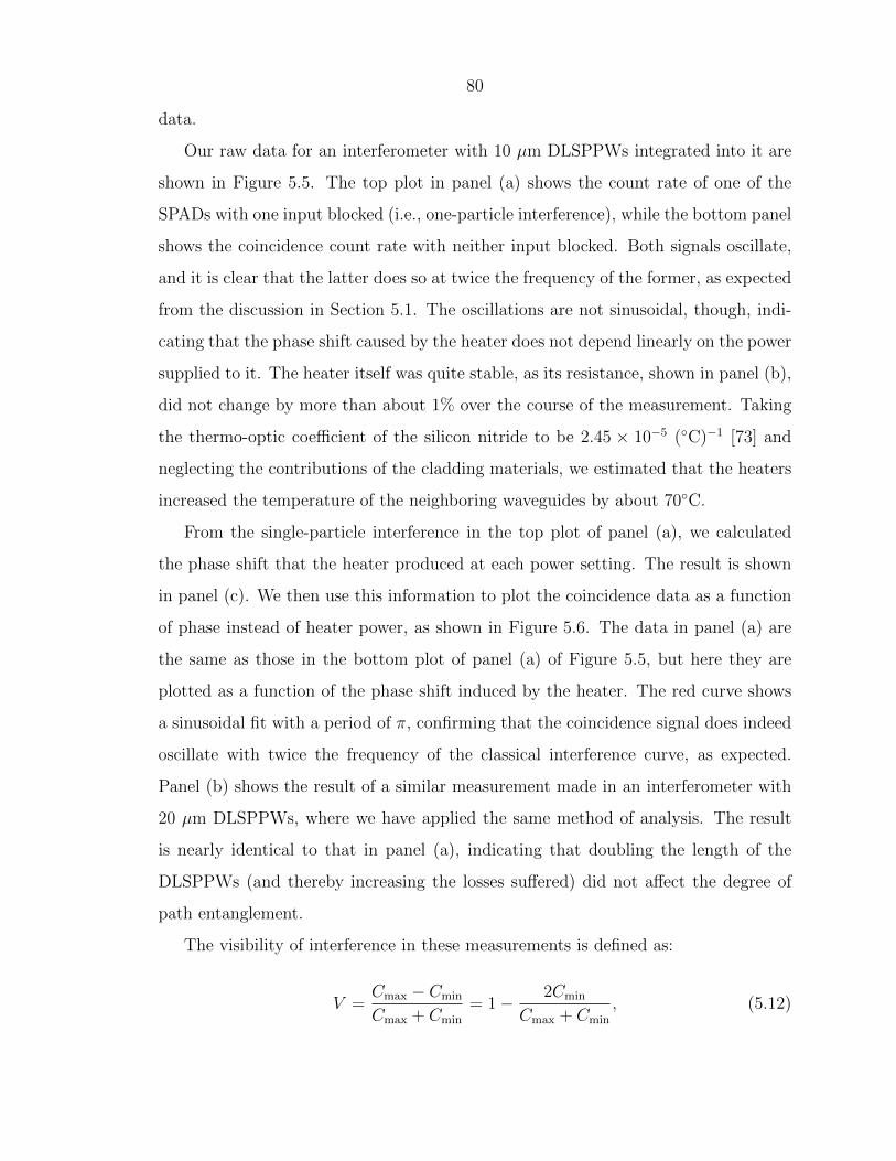
80
data.
Our raw data for an interferometer with 10 µm DLSPPWs integrated into it are
shown in Figure 5.5. The top plot in panel (a) shows the count rate of one of the
SPADs with one input blocked (i.e., one-particle interference), while the bottom panel
shows the coincidence count rate with neither input blocked. Both signals oscillate,
and it is clear that the latter does so at twice the frequency of the former, as expected
from the discussion in Section 5.1. The oscillations are not sinusoidal, though, indi-
cating that the phase shift caused by the heater does not depend linearly on the power
supplied to it. The heater itself was quite stable, as its resistance, shown in panel (b),
did not change by more than about 1% over the course of the measurement. Taking
the thermo-optic coefficient of the silicon nitride to be 2.45 × 10⁻⁵ (◦C)−1 [73] and
neglecting the contributions of the cladding materials, we estimated that the heaters
increased the temperature of the neighboring waveguides by about 70◦C.
From the single-particle interference in the top plot of panel (a), we calculated
the phase shift that the heater produced at each power setting. The result is shown
in panel (c). We then use this information to plot the coincidence data as a function
of phase instead of heater power, as shown in Figure 5.6. The data in panel (a) are
the same as those in the bottom plot of panel (a) of Figure 5.5, but here they are
plotted as a function of the phase shift induced by the heater. The red curve shows
a sinusoidal fit with a period of π, confirming that the coincidence signal does indeed
oscillate with twice the frequency of the classical interference curve, as expected.
Panel (b) shows the result of a similar measurement made in an interferometer with
20 µm DLSPPWs, where we have applied the same method of analysis. The result
is nearly identical to that in panel (a), indicating that doubling the length of the
DLSPPWs (and thereby increasing the losses suffered) did not affect the degree of
path entanglement.
The visibility of interference in these measurements is defined as:
V =Cmax − Cmin
Cmax + Cmin
= 1− 2Cmin
Cmax + Cmin
, (5.12)
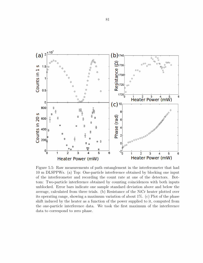
81
Figure 5.5: Raw measurements of path entanglement in the interferometer that had10 m DLSPPWs. (a) Top: One-particle interference obtained by blocking one inputof the interferometer and recording the count rate at one of the detectors. Bot-tom: Two-particle interference obtained by counting coincidences with both inputsunblocked. Error bars indicate one sample standard deviation above and below theaverage, calculated from three trials. (b) Resistance of the NiCr heater plotted overits operating range, showing a maximum variation of about 1%. (c) Plot of the phaseshift induced by the heater as a function of the power supplied to it, computed fromthe one-particle interference data. We took the first maximum of the interferencedata to correspond to zero phase.
82
Figure 5.6: Measurements of plasmonic path entanglement in 10 µm (left) and 20 µm(right) DLSPPWs with visibilities of 0.954 ± 0.016 and 0.948 ± 0.021, respectively.Each data point marks the average of three measurements, while the error bars rep-resent one sample standard deviation above and below the average. The red curvesare sinusoidal fits.
where Cmax and Cmin are the maximum and minimum count rates observed as the
phase varies. In the interferometer with 10 µm DLSPPWs we observed one-particle
and two-particle interference with visibilities of 0.974 ± 0.005 and 0.954 ± 0.016,
respectively. In each of these calculations, we estimated the standard deviation of the
visibility using the (measured) standard deviation of Cmin, taking Cmax to be constant
because fluctuations in Cmax are proportionately much smaller than fluctuations in
Cmin. In the circuit with 20 µm DLSPPWs, we observed visibilities of 0.972± 0.007
and 0.948± 0.021 for one- and two-particle interference, respectively.
While the longer, higher-loss waveguides did not reduce the visibility of entangle-
ment, they certainly reduced the overall transmission of light through the interfer-
ometers. As shown in Figure 5.6, increasing the length of the DLSPPWs by 10 µm
reduced the coincidence count rate by roughly a factor of five, which is consistent
with the observed drop in the single-particle signal by slightly more than a factor
of two. Previously we estimated the absorption length in similar waveguides to be
roughly 7 µm, however, which suggests that the difference between losses observed in
the 10 µm and 20 µm waveguides in the current experiment should have been larger.
We suspect that the coupling of light into and out of the interferometer with 20 µm
83
DLSPPWs might have been slightly more efficient than for the interferometer with
10 µm DLSPPWs, partially offsetting the extra absorption loss.
5.6 Summary and Outlook
From these measurements, my collaborators and I concluded that we had observed
path entanglement between surface plasmons with a visibility of approximately 95%.
Moreover, doubling the length of the plasmonic waveguides we studied did not have
any measurable effect on the visibility of entanglement. As a result, we concluded that
the plasmons in our experiment did not interact strongly enough with the metal that
sustained them—as by elastically scattering electrons or phonons, for example—to
decohere the path-entangled state.
While this experiment certainly does not rule out these kinds of interactions in
all plasmonic systems, it does suggest that they are all the more unlikely to occur
in similar waveguides. Future experiments might try to reproduce these results with
shorter wavelength down-converted photons, or in higher-loss, more more confined,
more dispersive waveguides, such as metal-insulator-metal slot waveguides. It is pos-
sible, for example, that operating on the more dispersive part of the surface plasmon
dispersion curve (see Figure 2.2), where the mode is less “light-like,” might reveal
more interesting physics. It might also be possible to perform an entanglement ex-
periment interrogating the plasmonic resonances of nanoparticles, for which theory
predicts that pure dephasing should be significant [24].
An alternative future direction for this work might focus instead on extending the
technology my collaborators and I developed for these experiments. Integrated quan-
tum photonics [74, 75, 76] has become an active field of research, with recent demon-
strations of single photon sources [77], quantum logic gates [78, 79], and single-photon
detectors [80, 81] integrated variously with silicon, silica, and III-V waveguides. To
combine these components into a single quantum photonics platform operating at a
single temperature presents a formidable challenge, but the promise of linear optical
quantum computing [82, 83] makes work towards this goal worthwhile. The exper-
84
imental methods developed for the present work, particularly related to the design
and fabrication of silicon nitride waveguides and associated components, might be
useful in such an undertaking.
85
Appendix: Fabrication Details
Note: These instructions refer to the tools and supplies available specifically at the
Kavli Nanoscience Institute at Caltech. The precise details (machine settins, bake
and etch times, and so on) ought to be taken as starting points for optimizing any
future process, as the optimal process parameters sometimes drift over time.
Fabrication Process for TPQI Experiment
1. Prepare a batch of chips from a new 4” wafer
(a) Obtain a new wafer.
For this work I used 4” Si(100) wafers with 3 µm of wet-thermal SiO2 and
300 nm of stoichiometric LPCVD Si3N4 grown on both sides. I ordered
them from Rogue Valley Microdevices, a foundry.
(b) Strip the oxynitride from the surface.
Submerge the wafer in buffered hydrofluoric acid (BHF) for 1-2 s, rinse it
thoroughly with DI water, and blow it dry with N2. I used a pre-mixed
BHF solution from Transene, which used ammonium fluoride as a buffer
and etched wet-thermal oxide at about 100 nm/min, roughly ten times
slower than concentrated HF.
(c) Prepare the wafer for photolithography.
Bake the wafer at 110◦C for 2 min to drive any adsorbed water off the
surface. Mount the wafer in a spin-coater and apply AZ 9245 photoresist
liberally. Spin the wafer at 500 rpm for 5 s (to distribute the resist), then
86
ramp the speed up to 4,000 rpm and leave it for 30 s. The photoresist
layer should be 4-5 µm thick. Clean any resist off of the back side using
swabs soaked with acetone, then bake the wafer at 110◦C for 3 min.
(d) Create the dicing pattern in the photoresist.
Find the 5” mask with the dicing pattern on it (see Chapter 3 for details).
Using one of the Karl Suss mask aligners, expose the wafer through this
mask for 20 s. Develop the wafer in a solution of AZ 400K that has been
diluted 1:2 in DI water (this usually takes 90-120 s). Rinse the wafer with
DI water and blow it dry with N2. Bake the wafer at 145◦C for 5 min,
then turn off the hotplate and let the wafer cool for an additional 5 min.
This “hard bake” drives any remaining solvent out of the resist, which is
important for plasma etching!
(e) Transfer the dicing pattern into the Si3N4 layer.
Apply 950 PMMA A11 to the back of the wafer using a swab. It is not
necessary to cover the entire surface; just apply enough to make good
thermal contact with the carrier wafer, covering maybe 10-20% of the
surface. (Note: DO NOT put a swab directly into the main bottle of
PMMA resist!! If there is a small brown bottle of it near the Oxford
etchers, use that one. Otherwise, decant a small amount from the main
bottle to use with the swab.) Stick the wafer down to a 6” Si carrier wafer
and bake it at 180◦C for 15-20 s to drive out most of the solvent. Etch the
wafer for 5 min in the Oxford 380 etcher using the following recipe:
“Jim - high rate Si (lower ICP power)”
• 100 sccm SF6
• 20/1500 W Fwd/ICP power
• 5 mTorr pressure
• 10◦C temperature
Soak the wafers in dichloromethane afterwards to dissolve the PMMA hold-
ing them together, and clean any PMMA residue from the back of the
87
device wafer using a swab soaked with acetone.
(f) Remove the Si3N4 layer from the back side of the wafer.
Repeat the procedure in (1c) to protect the top surface of the wafer with
AZ 9245 resist. Hard bake the wafer as before (but without patterning
it this time). Afterwards, use a swab soaked with acetone to remove any
residue from the back side. Use three or four drops of 950 PMMA A11
around the edge of the patterned (top) side, away from the pattern, to
stick the wafer upside down to a 6” Si carrier wafer. As before, bake the
wafers at 180◦C for 30 s, etch them for 5 min using the same etcher and
recipe, and soak them in acetone to separate them.
(g) Remove the SiO2 layer from the back side of the wafer.
Repeat the procedure in (1c) once more to protect the top surface of the
wafer, performing a hard bake at 145◦C as in the previous step. Clean
any residue from the back of the wafer using an acetone-soaked swab.
Carefully float the wafer on top of buffered HF so that only the back side
is in contact with the liquid. After 35 min, rinse the wafer thoroughly with
DI water and inspect the back side to make sure that no SiO2 remains.
Strip the photoresist with acetone and clean the wafer in piranha solution
(3:1 H2SO4:H2O2) to remove any organic residue left over from the previous
several steps.
(h) Thin the wafer to ∼200 µm.
Etch the wafer in a solution of ∼25% KOH at 90-100◦C (the temperature
will fluctuate) for ∼40 min, or until the wafer is about 200 µm thick. As
water evaporates from the KOH solution, replace it to keep the liquid level
about the same. I find that this step works best when I put the wafer
into the solution upside down. When the etch is finished, rinse the wafer
thoroughly (but carefully!) with DI water.
(i) Etch through the remaining SiO2 on the front side of the wafer.
In the previous step, the KOH should have etched through 1-2 µm of
88
the exposed SiO2 (i.e., in the patterned areas). Submerge the wafer in
concentrated HF (etch rate of ∼1 µm/min) for 1-2 min to remove the
remaining SiO2. Rinse the wafer thoroughly with DI water and blow it
dry with N2.
(j) Dice the wafer into individual chips.
Spin a layer of PMMA onto the top surface of the wafer to protect it from
debris during scribing. The exact thickness of PMMA does not matter,
but I usually use 950 PMMA A4 or A6 with a 2 min pre-bake and a 5 min
bake, both at 180◦C. Use the Dynatex scriber to scribe along the streets
of the dicing pattern with the scribe force set to 2000 and the scribe angle
set to 32◦. The sticky green film that we use to mount wafers in this tool
adheres to the wafer very strongly, which makes it very difficult to remove
a large, thin wafer without breaking it. For this reason, I usually cut an
extra ∼3.5” square of the film and place it face-down in the center of the
mounting ring before mounting the wafer, so that the center of the wafer
does not stick to the film underneath. After scribing, carefully (!!) remove
the wafer from the film and break it along the scribed lines using a glass
slide. For the longer breaks, half of a 6” wafer works better than a glass
slide. Rinse each chip with IPA to remove the debris from scribing.
2. Create dielectric waveguides in the Si3N4 layer.
(a) Prepare a chip for e-beam lithography.
Soak one of the chips from the previous step in dichloromethane to remove
the PMMA protective layer. Clean it with piranha solution to remove
residual organics, rinse it thoroughly with DI water (because sulphuric acid
solutions can sometimes leave a residue), and dip it in BHF to strip the
surface oxynitride. Rinse the chip thoroughly again and blow it dry with
N2. Bake it for 2 min at 180◦C, and then spin ma-N 2403, a negative-tone
e-beam resist, at 3,000 rpm to form a layer ∼300 nm thick. Occasionally
89
there will bubbles or particles in the film, so inspect it with an optical
microscope and strip it with acetone if it is necessary to try again. Bake
the chip at 95◦C for 1 min 30 s.
(b) Write the dielectric waveguide layer using the EBPG.
I find that the patterns I usually write are sparse enough that I do not
need to correct for the proximity effect. Rather, it is sufficient to use a flat
fracture (i.e., a uniform dose) with a resolution of 5 nm. Write the pattern
with a 3 nA beam at a dose of 530 µC/cm2, aligning to at least one of
the four square markers in the dicing layer. Develop the chip in MF-319
developer for 25 s.
(c) Transfer the pattern into the Si3N4 layer.
Clean the 380 with Ar for 5 min and O2 for 10 min, and then condition it
using the following recipe for 15 min:
“Jim - nitride pBosch (faster)”
• 38 sccm SF6, 52 sccm C4F8
• 24/1000 W Fwd/ICP power
• 10 mTorr pressure
• 10◦C temperature
While these cleaning and conditioning etches are running, measure the
thickness of the nitride layer using the Filmetrics normal-incidence reflec-
tometer. Using a cleanroom swab, apply a small dot of Fomblin oil to the
center of the back side of the chip and carefully stick the chip down to
a 6” carrier wafer. There should be enough oil to hold the chip in place
when the carrier wafer is held vertically, but not so much that it oozes out
around the edges of the chip. Etch the chip until only 15-20 nm of nitride
remains (about 4 min 15 s). To measure the thickness of the remaining ni-
tride, measure the same location as before with the Filmetrics instrument
and fix the thickness of the oxide layer to that which you measured previ-
ously. This method seems to give surprisingly accurate measurements of
90
even very thin layers of silicon nitride on several microns of oxide. When
this step is complete (which will likely take two etches), clean the chamber
with an oxygen plasma for 15 min and then strip the remaining resist with
a 2 min oxygen etch.
3. Create recessed gold pads for the DLSPPWs.
(a) Prepare the chip for e-beam lithography.
Bake the chip at 180◦C for 2 min to drive away adsorbed water. Spin
495 PMMA A8 at 3,000 rpm to form a layer that is ∼500 nm thick. Bake
the chip at 150◦C for 5 min.
(b) Write rectangles for the gold pads using the EBPG.
Fracture the pattern at 10 nm resolution using the Proximity Effect Cor-
rection (PEC) module in Layout Beamer. Write the pattern using a ∼5 nA
beam with a base dose of 1400 µC/cm2, aligning it to the markers in the
previous pattern. Develop the chip for 45 s in 1:3 MIBK:IPA, rinse it with
IPA, and blow it dry with N2.
(c) Etch through the remaining Si3N4.
Etch through the remaining ∼20 nm of Si3N4 with XeF2 using the following
settings:
• 2000 mTorr pulse pressure
• 30 s pulse duration
• 10 mTorr base pressure
Two pulses should be sufficient, but I usually use four pulses just to make
sure all of the nitride is removed. Xenon difluoride does not attack PMMA
at all and etches thermal SiO2 orders of magnitude more slowly than Si3N4.
(d) Etch ∼150 nm into the underlying oxide.
Measure the height of the resist above the exposed oxide (ideally on a test
feature far away from the actual patterns) using the profilometer. Etch
91
the chip for 90 s in buffered HF, rinse it thoroughly, and blow it dry.
Measure the height of the oxide above the resist again and subtract the
measurement from before the HF etch; the difference should be ∼150 nm.
(e) Deposit gold.
Of the three e-beam evaporators in the KNI, the Lesker gives the best
results for this step by far. Its crucibles are smaller and farther away
from the sample than on the other evaporators, so evaporated material is
deposited at closest to normal incidence. This is optimal for metal lift-off.
Deposit a 5 nm Ti layer at 0.5 A/s to improve adhesion between the gold
and the underlying oxide, and then deposit enough gold (∼145 nm) to
completely fill in the hole etched during the previous step. I use a depo-
sition rate of 2 A/s. Immerse the chip in dichloromethane to dissolve the
PMMA and lift off the gold. The resulting gold pads should be recessed
into the surface so that their top surfaces are within ∼20 nm of being flush
with the rest of the chip.
4. Pattern the spot-size converters and DLSPPWs in PMMA.
(a) Prepare the chip for e-beam lithography.
As before, pre-bake the chip at 180◦C for 2 min to drive away adsorbed
water. Spin 950 PMMA A11 at 3,000 rpm to form a layer that is ∼2.2 µm
thick. Bake the chip at 150◦C for 5 min.
(b) Clear the PMMA from around the gold pads.
Write a large rectangle to clear away the thick layer of PMMA from within
250 µm of the gold pads. Precision is not important in this step, so I
fracture at 50 nm resolution and use a large beam (150-250 nA). Because
950 PMMA A11 is so thick, it requires a higher dose; use 2000 µC/cm2 to
be safe. Develop the chip in 1:3 MIBK:IPA for 45 s, rinse it with IPA, and
blow it dry.
(c) Spin a thinner layer of PMMA for the DLSPPWs.
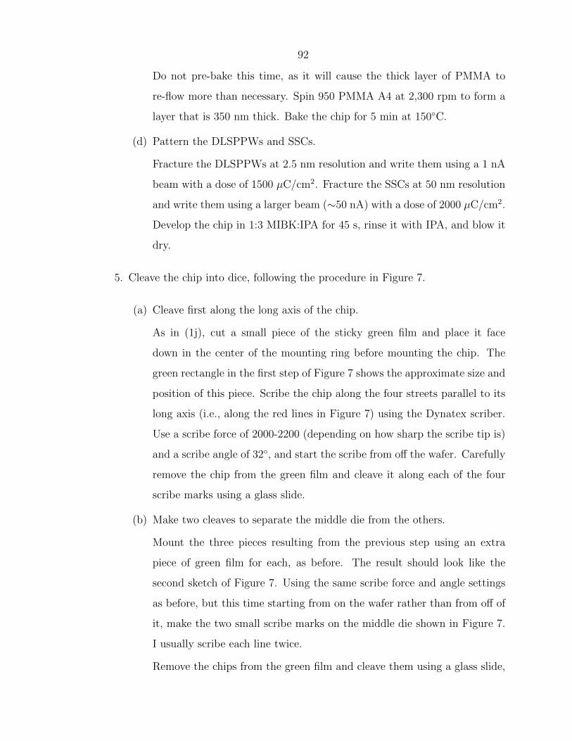
92
Do not pre-bake this time, as it will cause the thick layer of PMMA to
re-flow more than necessary. Spin 950 PMMA A4 at 2,300 rpm to form a
layer that is 350 nm thick. Bake the chip for 5 min at 150◦C.
(d) Pattern the DLSPPWs and SSCs.
Fracture the DLSPPWs at 2.5 nm resolution and write them using a 1 nA
beam with a dose of 1500 µC/cm2. Fracture the SSCs at 50 nm resolution
and write them using a larger beam (∼50 nA) with a dose of 2000 µC/cm2.
Develop the chip in 1:3 MIBK:IPA for 45 s, rinse it with IPA, and blow it
dry.
5. Cleave the chip into dice, following the procedure in Figure 7.
(a) Cleave first along the long axis of the chip.
As in (1j), cut a small piece of the sticky green film and place it face
down in the center of the mounting ring before mounting the chip. The
green rectangle in the first step of Figure 7 shows the approximate size and
position of this piece. Scribe the chip along the four streets parallel to its
long axis (i.e., along the red lines in Figure 7) using the Dynatex scriber.
Use a scribe force of 2000-2200 (depending on how sharp the scribe tip is)
and a scribe angle of 32◦, and start the scribe from off the wafer. Carefully
remove the chip from the green film and cleave it along each of the four
scribe marks using a glass slide.
(b) Make two cleaves to separate the middle die from the others.
Mount the three pieces resulting from the previous step using an extra
piece of green film for each, as before. The result should look like the
second sketch of Figure 7. Using the same scribe force and angle settings
as before, but this time starting from on the wafer rather than from off of
it, make the two small scribe marks on the middle die shown in Figure 7.
I usually scribe each line twice.
Remove the chips from the green film and cleave them using a glass slide,
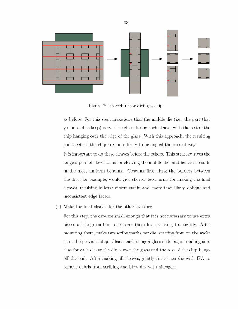
93
Figure 7: Procedure for dicing a chip.
as before. For this step, make sure that the middle die (i.e., the part that
you intend to keep) is over the glass during each cleave, with the rest of the
chip hanging over the edge of the glass. With this approach, the resulting
end facets of the chip are more likely to be angled the correct way.
It is important to do these cleaves before the others. This strategy gives the
longest possible lever arms for cleaving the middle die, and hence it results
in the most uniform bending. Cleaving first along the borders between
the dice, for example, would give shorter lever arms for making the final
cleaves, resulting in less uniform strain and, more than likely, oblique and
inconsistent edge facets.
(c) Make the final cleaves for the other two dice.
For this step, the dice are small enough that it is not necessary to use extra
pieces of the green film to prevent them from sticking too tightly. After
mounting them, make two scribe marks per die, starting from on the wafer
as in the previous step. Cleave each using a glass slide, again making sure
that for each cleave the die is over the glass and the rest of the chip hangs
off the end. After making all cleaves, gently rinse each die with IPA to
remove debris from scribing and blow dry with nitrogen.
94
Fabrication Process for Entanglement Experiment
1. Follow the procedures in (1) and (2) from the previous section to prepare a chip
with nitride waveguides.
2. Create recessed gold pads for the DLSPPWs, following the procedure in (3)
from the previous section.
(Note: This step can be performed after step (5) if desired. I like to do it as
early in the process as possible, however, in case there are problems with the
etching or gold deposition. It’s best to have invested as little time as possible
before attempting a difficult step like this one!)
3. Etch holes between the interferometers to use for undercutting the heaters in
subsequent steps.
(a) Clean the chip with piranha solution.
Rinse it thoroughly (but carefully!) with DI water and blow it dry. Clean-
ing the chip this way will ensure that the photoresist in the next step will
adhere well during the subsequent HF etch.
(b) Prepare the chip for photolithography.
Strip the native oxynitride from the surface using buffered HF. Bake the
chip for 2 min at 110◦C. Spin AZ 9245 photoresist at 3,000 rpm and bake
it for 3 min at 110◦C.
(c) Pattern the resist.
Find the photomask that has 300 µm × 8 µm holes in between the interfer-
ometers. Follow the procedure in (1d) from the previous section to transfer
this pattern into the resist. As before, perform a hard-bake at 145◦C for
5 min, then turn off the hotplate and let the chip cool for another 5 min
before removing it. Use an acetone-soaked swab to remove any residue
from the back of the chip.
(d) Remove the remaining silicon nitride from the patterned areas.
95
As described above, use a small amount of Fomblin oil to stick the chip
down to a 6” carrier wafer. Etch the sample for 20 s in the 380 using the
following recipe:
“Jim - high rate Si (lower ICP power)”
• 100 sccm SF6
• 20/1500 W Fwd/ICP power
• 5 mTorr pressure
• 10◦C temperature
Remove the remaining Fomblin oil from the back side of the chip using a
swab soaked with IPA.
(e) Etch through the thermal oxide, down to the underlying silicon.
Dip the chip in a dilute solution of Triton X-100 surfactant in DI wa-
ter (a concentration of roughly 0.1% seems to work well), then etch it
in buffered HF long enough to get through the thermal oxide. Using
Transene’s Buffered HF Improved, this takes about 30 min, though I usu-
ally etch for an extra 3-5 min to be sure I’ve removed all the oxide. The
surfactant is crucial to ensure that the HF actually wets the features to
be etched; without it, surface tension will keep the HF from getting down
into micron-scale holes in the (very hydrophobic) photoresist.
(f) Remove the photoresist.
Strip the photoresist with acetone, rinse the chip with IPA, and blow it dry.
Afterwards, clean it with piranha solution to remove any organic residue.
4. Add NiCr heaters.
(a) Prepare the chip for e-beam lithography.
Bake the chip at 180◦C for 2 min to drive water off its surface. Spin
495 PMMA A8 at 3,000 rpm and bake the chip at 150◦C for 5 min, forming
a layer that is ∼500 nm thick. Next, spin 950 PMMA A2 at 3,000 rpm and
96
bake again at 150◦C. These two layers of resist, the bottom one slightly
more sensitive to electron-beam exposure than the top one, will help ensure
the NiCr lifts off cleanly.
(b) Write the heaters using the EBPG.
Fracture the heater pattern at 10 nm resolution (no PEC) and write it using
a 10 nA beam at a dose of 2000 µC/cm2, aligning to the gold markers from
the previous layer. Develop the chip in 1:3 MIBK:IPA for 45 s, rinse it
with IPA, and blow it dry.
(c) Deposit NiCr.
I use the TES for this step, but the CHA should work too. Evapo-
rate 200 nm of NiCr (80% Ni) at a rate of 2 A/s. Soak the chip in
dichloromethane for ∼15 min to lift off the metal from around the pat-
terned areas, leaving the heaters. Rinse the chip with IPA and blow it
dry.
5. Add gold contacts for the heaters.
(a) Prepare the chip for e-beam lithography using the same two-layer PMMA
resist as in (4a).
(b) Write the contact pads using the EBPG.
Fracture the pattern at 50 nm resolution using the Proximity Effect Correc-
tion (PEC) module in Layout Beamer. Write the resulting pattern using a
large beam (i.e., ∼200 nA) and a dose of 1400 µC/cm2. As before, develop
in 1:3 MIBK:IPA for 45 s.
(c) Deposit gold.
Using the TES or CHA, evaporate 5 nm of Cr at 0.5 A/s as an adhe-
sion layer, followed by 300 nm of Au at 2 A/s. Lift off the gold film in
dichloromethane, as before.
6. Prepare the final PMMA layers.
97
(a) Prepare the thick PMMA layer.
Bake the chip at 150◦C for 2 min. Spin 950 PMMA A11 at 3,000 rpm and
bake it at 150◦C for 5 min.
(b) Clear the PMMA from around the gold pads for the DLSPPWs, as in (4b)
from the previous section.
(c) Prepare the thin PMMA layer.
Do not pre-bake this time. Spin 950 PMMA A4 at 2,300 rpm to form a
layer that is 350 nm thick. Bake the chip at 150◦C for 5 min.
(d) Remove the PMMA from the holes etched in step (3).
Fracture the pattern (which contains rectangles that cover these holes) at
50 nm resolution and write it using a 50 nA beam at a dose of 2,500 µC/cm2.
Develop the chip in 1:3 MIBK:IPA for 45 s.
7. Etch the silicon from underneath the heaters.
(a) Strip the native oxide from the silicon.
Vent the XeF2 etcher, following the usual procedure. Dip the chip in
buffered HF, rinse it thoroughly with water, and blow it dry. Quickly
load the chip into the load lock of the XeF2 etcher before the native oxide
regrows.
(b) Etch the chip using XeF2.
Use 4-7 pulses, depending on the desired extent of the undercut, each 30 s
in duration at a pressure of 2,000 mTorr.
8. Write the spot-size converters and DLSPPWs using the EBPG.
Fracture the DLSPPWs at 2.5 nm resolution (no PEC) and write them using a
1 nA beam at a dose of 1500 µC/cm2. Fracture the SSCs at 50 nm resolution (no
PEC) and write them using a large beam (∼200 nA) at a dose of 1800 µC/cm2.
Develop the chip in 1:3 MIBK:IPA for 45 s, rinse it with IPA, and gently blow
it dry with N2.
98
9. Dice the chip as in (5), making sure to handle the chip as carefully as possible
to prevent the undercut structures from breaking.
99
Bibliography
[1] S. J. Freedman and J. F. Clauser. Experimental test of local hidden-variable
theories. Phys. Rev. Lett., 28:938–941, 1972.
[2] A. Aspect, P. Grangier, and G. Roger. Experimental realization of Einstein-
Podolsky-Rosen-Bohm gedankenexperiment: A new violation of Bell’s inequali-
ties. Phys. Rev. Lett., 49:91–94, 1982.
[3] L.-A. Wu, M. Xiao, and H. J. Kimble. Squeezed states of light from an optical
parametric oscillator. J. Opt. Soc. Am. B, 4:1465–1475, 1987.
[4] D. T. Smithey, M. Beck, J. Cooper, and M. G. Raymer. Measurement of number-
phase uncertainty relations of optical fields. Phys. Rev. A, 48:3159–3167, 1993.
[5] M. Brune, E. Hagley, J. Dreyer, X. Maitre, A. Maali, C. Wunderlich, J. M.
Raimond, and S. Haroche. Observing the progressive decoherence of the “meter”
in a quantum measurement. Phys. Rev. Lett., 77:4887–4890, 1996.
[6] M. Schlosshauer. Decoherence, the measurement problem, and interpretations
of quantum mechanics. Rev. Mod. Phys., 76:1267–1305, 2004.
[7] M. Schlosshauer. Decoherence and the quantum-to-classical transition. Springer,
2008.
[8] W. Langbein, P. Borri, U. Woggon, V. Stavarache, D. Reuter, and A. D. Wleck.
Radiatively limited dephasing in InAs quantum dots. Phys. Rev. B, 70:033301,
2004.
100
[9] C. Langer, R. Ozeri, J. D. Jost, J. Chiaverini, B. DeMarco, A. Ben-Kish, R. B.
Blakestad, J. Britton, D. B. Hume, W. M Itano, D. Leibfried, R. Reichie,
T. Rosenband, T. Schaetz, P. O. Schmidt, and D. J. Wineland. Long-lived
qubit memory using atomic ions. Phys. Rev. Lett., 95:060502, 2005.
[10] E. Pazy, E. Biolatti, T. Calarco, I. D’Amico, P. Zanardi, F. Rossi, and P. Zoller.
Spin-based optical quantum computation via Pauli blocking in semiconductor
quantum dots. Europhys. Lett., 62:175, 2003.
[11] H. Paik, D. I. Schuster, L. S. Bishop, G. Kirchmair, G. Catelani, A. P. Sears,
B. R. Johnson, M. J. Reagor, L. Frunzio, L. I. Glazman, S. M. Girvin, M. H.
Devoret, and R. J. Schoelkopf. Observation of high coherence in Josephson
junction qubits measured in a three-dimensional circuit QED architecture. Phys.
Rev. Lett., 107:240501, 2011.
[12] C. Rigetti, J. M. Gambetta, S. Poletto, B. L. T. Plourde, J. M. Chow, A. D.
Corcoles, J. A. Smolin, S. T. Merkel, J. R. Rozen, G. A. Keefe, M. B. Rothwell,
M. B. Ketchen, and M. Steffen. Superconducting qubit in a waveguide cavity
with a coherence time approaching 0.1 ms. Phys. Rev. B, 86:100506, 2012.
[13] P. G. Kwiat, K. Mattle, H. Weinfurter, and A. Zeilinger. New high-intensity
source of polarization-entangled photon pairs. Phys. Rev. Lett., 75:4337–4341,
1995.
[14] P. G. Kwiat, E. Waks, A. G White, I. Appelbaum, and P. H. Eberhard. Ultra-
bright source of polarization-entangled photons. Phys. Rev. A, 60:R773–R776,
1999.
[15] P. G. Kwiat, W. A. Vareka, C. K. Hong, H. Nathel, and R. Y. Chiao. Correlated
two-photon interference in a dual-beam Michelson interferometer. Phys. Rev. A,
41:2910–2913, 1990.
[16] Z. Y. Ou, X. Y. Zou, L. J. Wang, and L. Mandel. Observation of nonlocal
interference in separated photon channels. Phys. Rev. Lett., 65:321–324, 1990.
101
[17] K. Edamatsu, R. Shimizu, and T. Itoh. Measurement of the photonic de
Broglie wavelength of entangled photon pairs generated by spontaneous para-
metric down-conversion. Phys. Rev. Lett., 89:213601, 2002.
[18] R. Ursin, F. Tiefenbacher, T. Schmitt-Manderbach, H. Weier, T. Scheidl, M. Lin-
denthal, B. Blauensteiner, T. Jennewein, J. Perdigues, P. Trojeck, B. Omer,
M. Furst, J. R. Meyenburg, Z. Sodnik, C. Barbieri, H. Weinfurter, and
A. Zeilinger. Entanglement-based quantum communication over 144 km. Nature
Phys., 3:481–486, 2007.
[19] S. A. Maier and H. A. Atwater. Plasmonics: Localization and guiding of elec-
tromagnetic energy in metal/dielectric structures. J. Appl. Phys., 98:011101,
2005.
[20] J. A. Schuller, E. S. Barnard, W. S. Cai, Y. C. Jun, J. S. White, and M. L.
Brongersma. Plasmonics for extreme light concentration and manipulation. Na-
ture Mat., 9:193–204, 2010.
[21] M. I. Stockman. Nanoplasmonics: past, present, and glimpse into future. Opt.
Exp., 19:22029–22106, 2011.
[22] C. Sonnichsen, T. Franzl, T. Wilk, G. von Plessen, and J. Feldmann. Drastic
reduction of plasmon damping in gold nanorods. Phys. Rev. Lett., 88:077402,
2002.
[23] M. Scharte, R. Porath, T. Ohms, M. Aeschlimann, B. Lamprecht, H. Ditlbacher,
and F. R. Aussenegg. Lifetime and dephasing of plasmons in Ag nanoparticles.
In Proc. SPIE 4456, Controlling and using light in nanometric domains, 2001.
[24] Z. Guo, B. F. Habenicht, W.-Z. Liang, and O. V. Prezhdo. Ab initio study of
phonon-induced dephasing of plasmon excitations in silver quantum dots. Phys.
Rev. B, 81:125415, 2010.
[25] N. W. Ashcroft and N. D. Mermin. Solid State Physics. Thomson Learning, Inc.,
1976.
102
[26] M. Liu, M. Pelton, and P. Guyot-Sionnest. Reduced damping of surface plasmons
at low temperatures. Phys. Rev. B, 79:035418, 2009.
[27] J. M. Pitarke, V. M. Silkin, E. V. Chulkov, and P. M. Echenique. Theory of
surface plasmons and surface-plasmon polaritons. Rep. Prog. Phys., 70:1–87,
2007.
[28] J. M. Elson and R. H. Ritchie. Photon interactions at a rough metal surface.
Phys. Rev. B, 4:4129–4138, 1971.
[29] D. Ballester, M. S. Tame, and M. S. Kim. Quantum theory of surface-plasmon
polariton scattering. Phys. Rev. A, 82:012325, 2010.
[30] Z. Jacob. Quantum plasmonics. MRS Bulletin, 37:761–767, 2012.
[31] M. S. Tame, K. R. McEnery, S. K. Ozdemir, J. Lee, S. A. Maier, and M. S. Kim.
Quantum plasmonics. Nature Phys., 9:329–340, 2013.
[32] A. V. Akimov, A. Mukherjee, C. L. Yu, D. E. Chang, A. S. Zibrov, P. R. Hemmer,
H. Park, and M. D. Lukin. Generation of single optical plasmons in metallic
nanowires coupled to quantum dots. Nature, 450:402–406, 2007.
[33] R. W. Heeres, S. N. Dorenbos, B. Koene, G. S. Solomon, L. P. Kouwenhoven,
and V. Zwiller. On-chip single plasmon detection. Nano Lett., 10:661–664, 2010.
[34] R. Kolesov, B. Grotz, G. Balasubramanian, R. Stohr, A. A. L. Nicolet, P. R.
Hemmer, F. Jelezko, and Jorg Wratchup. Wave-particle duality of single surface
plasmon polaritons. Nature Phys., 5:470–474, 2009.
[35] G. Di Martino, Y. Sonnefraud, S. Kena-Cohen, M. Tame, S. K. Ozdemir, M. S.
Kim, and S. A. Maier. Quantum statistics of surface plasmon polaritons in
metallic stripe waveguides. Nano Lett., 12:2504–2508, 2012.
[36] E. Altewischer, M. P. van Exter, and J. P. Woerdman. Plasmon-assisted trans-
mission of entangled photons. Nature, 418:304–306, 2002.
103
[37] E. Moreno, F. J. Garcia-Vidal, D. Ernl, J. I. Cirac, and L. Martin-Moreno.
Theory of plasmon-assisted transmission of entangled photons. Phys. Rev. Lett.,
92:236801, 2004.
[38] S. Fasel, F. Robin, E. Moreno, D. Ernl, N. Gisin, and H. Zbinden. Energy-time
entanglement preservation in plasmon-assisted light transmission. Phys. Rev.
Lett., 94:110501, 2005.
[39] S. Fasel, M. Halder, N. Gisin, and H. Zbinden. Quantum superposition and
entanglement of mesoscopic plasmons. New J. Phys., 8:1–8, 2006.
[40] A. Huck, S. Smolka, P. Lodahl, A. S. Sorensen, A. Boltasseva, J. Janousek, and
U. L. Andersen. Demonstration of quadrature-squeezed surface plasmons in a
gold waveguide. Phys. Rev. Lett., 102:246802, 2009.
[41] C. K. Hong, Z. Y. Ou, and L. Mandel. Measurement of subpicosecond time
intervals between two photons by interference. Phys. Rev. Lett., 59:2044–2046,
1987.
[42] Z. Y. Ou and L. Mandel. Derivation of reciprocity relations for a beam splitter
from energy balance. Am. J. Phys., 57:66–68, 1989.
[43] A. Kuhn, M. Hennrich, and G. Rempe. Deterministic single-photon source for
distributed quantum networking. Phys. Rev. Lett., 89:067901, 2002.
[44] T. Legero, T. Wilk, A. Kuhn, and G. Rempe. Time-resolved two-photon quantum
interference. Appl. Phys. B, 77:797–802, 2003.
[45] M. Beck. Comparing measurements of g(2)(0) performed with different coinci-
dence detection techniques. J. Opt. Soc. Am. B, 24:2972–2978, 2007.
[46] A. Yariv. Quantum Electronics, chapter 16. John Wiley & Sons, 3rd edition,
1989.
104
[47] R. Lettow, Y. L. A. Rezus, A. Renn, G. Zumofen, E. Ikonen, S. Gotzinger, and
V. Sandoghdar. Quantum interference from tunably indistinguishable photons
from remote organic molecules. Phys. Rev. Lett., 104:123605, 2010.
[48] E. B. Flagg, A. Muller, S. V. Polyakov, A. Ling, A. Migdall, and G. S. Solomon.
Interference of single photons from two separate semiconductor quantum dots.
Phys. Rev. Lett., 104:137401, 2010.
[49] R. B. Patel, A. J. Bennett, I. Farrer, C. A. Nicoll, D. A. Ritchie, and A. J.
Shields. Two-photon interference of the emission from electrically tunable remote
quantum dots. Nature Photon., 4:632–635, 2010.
[50] S. I. Bozhevolnyi, V. S. Volkov, E. Devaux, and T. W. Ebbesen. Channel
plasmon-polariton guiding by subwavelength metal grooves. Phys. Rev. Lett.,
95:046802, 2005.
[51] J. Wen, P. Banzer, A. Kriesch, D. Ploss, B. Schmauss, and U. Peschel. Exper-
imental cross-polarization detection of couplin far-field light to highly confined
plasmonic gap modes via nanoantennas. Appl. Phys. Lett., 98:101109, 2011.
[52] A. Kriesch, S. P. Burgos, D. Ploss, H. Pfeifer, H. A. Atwater, and U. Peschel.
Functional plasmonic nanocircuits with low insertion and propagation losses.
Nano Lett., 13:4539–4545, 2013.
[53] R. M. Briggs, J. Grandidier, S. P. Burgos, E. Feigenbaum, and H. A. Atwa-
ter. Efficient coupling between dielectric-loaded plasmonic and silicon photonic
waveguides. Nano Lett., 10:4851–4857, 2010.
[54] T. Shoji, T. Tsuchizawa, T. Watanabe, K. Yamada, and H. Morita. Low loss
mode size converter from 0.3 µm square si wire waveguides to single mode fibers.
Electron. Lett., 38:1669–1670, 2002.
[55] T. Wahlbrink, W. S. Tsai, M. Waldow, M. Forst, J. Bolten, T. Mollenhauer,
and H. Kurz. Fabrication of high efficiency SOI taper structures. Microelectron.
Eng., 86:1117–1119, 2009.
105
[56] D. Taillaert, P. Bienstman, and R. Baets. Compact efficient broadband grating
coupler for silicon-on-insulator waveguides. Opt. Lett., 29:2749–2751, 2004.
[57] C. Zhang, J.-H. Sun, X. Xiao, W.-M. Sun, X.-J. Zhang, T. Chu, J.-Z. Yu, and
Y.-D. Yu. High efficiency grating coupler for coupling between single-mode fiber
and SOI waveguides. Chinese Phys. Lett., 30:014207, 2013.
[58] H. Seidel, L. Csepregi, A. Heuberger, and H. Baumgartel. Anisotropic etching of
crystalline silicon in alkaline solutions—II. Influence of dopants. J. Electrochem.
Soc., 137:3626–3632, 1990.
[59] T. H. P. Chang. Proximity effect in electronbeam lithography. J. Vac. Sci.
Technol., 12:1271–1275, 1975.
[60] M. D. Henry. ICP etching of silicon. PhD thesis, California Institute of Tech-
nology, 2010.
[61] L. G. Feinstein and M. J. Bill. Reduction of nodules in electron-gun-evaporated
Au films. J. Vac. Sci. Technol., 12:704–708, 1975.
[62] J. J. Thorn, M. S. Neel, V. W. Donato, G. S. Bergreen, R. E. Davies, and
M. Beck. Observing the quantum behavior of light in an undergraduate labora-
tory. Am. J. Phys., 72:1210–1219, 2004.
[63] Y.-H. Kim and W. P. Grice. Quantum interference with distinguishable photons
through indistinguishable pathways. J. Opt. Soc. Am. B, 22:493–498, 2005.
[64] R. W. Heeres, L. P. Kouwenhoven, and V. Zwiller. Quantum interference in
plasmonic circuits. Nature Nanotech., 8:719–722, 2013.
[65] X.-F. Ren, G.-P. Guo, Y.-F. Wang, Z.-W. Wang, and G.-C. Guo. Plasmon
assisted transmission of single photon wavepacket. Metamaterials, 1:106–109,
2007.
[66] S. M. Wang, S. Y. Mu, C. Zhu, Y. X. Gong, P. Xu, H. Liu, T. Li, S. N. Zhu,
and X. Zhang. Hong-Ou-Mandel interference mediated by the magnetic plasmon
106
waves in a three-dimensional optical metamaterial. Opt. Express, 20:5213–5218,
2012.
[67] G. Fuji, T. Segawa, S. Mori, N. Namekata, D. Fukuda, and S. Inoue. Preserva-
tion of photon indistinguishability after transmission through surface-plasmon-
polariton waveguide. Opt. Lett., 37:1535–1537, 2012.
[68] G. Di Martino, Y. Sonnefraud, M. S. Tame, S. Kena-Cohen, F. Dieleman, S. K.
Ozdemir, M. S. Kim, and S. A. Maier. Observation of quantum interference in
the plasmonic Hong-Ou-Mandel effect. Phys. Rev. Applied, 1:034004, 2014.
[69] Y.-J. Cai, M. Li, X.-F. Ren, C.-L. Zou, X. Xiong, H.-L. Lei, B.-H. Liu, G.-
P. Guo, and G.-C. Guo. High-visibility on-chip quantum interference of single
surface plasmons. Phys. Rev. Applied, 2:014004, 2014.
[70] S. M. Barnett, J. Jeffers, A. Gatti, and R. Loudon. Quantum optics of lossy
beam splitters. Phys. Rev. A, 57:2134–2145, 1998.
[71] Z. Y. Ou, E. C. Gage, B. E. Magill, and L. Mandel. Fourth-order interference
technique for determining the coherence time of a light beam. J. Opt. Soc. Am.
B, 6:100–103, 1989.
[72] K. Hornberger, S. Uttenthaler, B. Brezger, L. Hackermuller, M. Arndt, and
A. Zeilinger. Collisional decoherence observed in matter wave interferometry.
Phys. Rev. Lett., 90:160401, 2003.
[73] A. Arbabi and L. L. Goddard. Measurements of the refractive indices and thermo-
optic coefficients of Si3N4 and SiOx using microring resonances. Opt. Lett.,
38:3878–3881, 2013.
[74] J. L. O’Brien, A. Furusawa, and J. Vuckovic. Photonic quantum technologies.
Nature Photon., 3:687–695, 2009.
[75] A. Politi, J. C. F. Matthews, M. G. Thompson, and J. L. O’Brien. Integrated
quantum photonics. IEEE J. Sel. Top. Quantum Electron., 15:1673–1684, 2009.
107
[76] S. Tanzilli, A. Martin, F. Kaiser, M. P. De Micheli, O. Alibart, and D. B. Os-
trowsky. On the genesis and evolution of integrated quantum optics. Laser
Photonics Rev., 6:115–143, 2012.
[77] J. W. Silverstone, D. Bonneau, K. Ohira, N. Suzuki, H. Yoshida, N. Iizuka,
M. Ezaki, C. M. Natarajan, M. G. Tanner, R. H. Hadfield, V. Zwiller, G. D.
Marshall, J. G. Rarity, J. L. O’Brien, and M. G. Thompson. On-chip quantum
interference between silicon photon-pair sources. Nature Photon., 8:104–108,
2014.
[78] P. J. Shadbolt, M. R. Verde, A. Peruzzo, A. Politi, A. Laing, M. Lobino, J. C. F.
Matthews, M. G. Thompson, and J. L. O’Brien. Generating, manipulating and
measuring entanglement and mixture with a reconfigurable photonic circuit. Na-
ture Photon., 6:45–49, 2012.
[79] B. J. Metcalf, N. Thomas-Peter, J. B. Spring, D. Kundys, M. A. Broome, P. C.
Humphreys, X.-M. Jin, M. Barbieri, W. S. Kolthammer, J. C. Gates, B. J. Smith,
N. K. Langford, P. G. R. Smith, and I. A. Walmsley. Multiphoton quantum
interference in a multiport integrated photonic device. Nat. Commun., 4:1356,
2012.
[80] J. P. Sprengers, A. Gaggero, D. Sahin, S. Jahanmirinejad, G. Frucci, F. Mattioli,
R. Leoni, J. Beetz, M. Lermer, M. Kamp, S. Hofling, R. Sanjines, and A. Fiore.
Waveguide superconducting single-photon detectors for integrated quantum pho-
tonic circuits. Appl. Phys. Lett., 99:181110, 2011.
[81] C. Schuck, W. H. P. Pernice, and H. X. Tang. Waveguide integrated low noise
NbTiN nanowire single-photon detectors with milli-Hz dark count rate. Sci.
Rep., 3:1893, 2013.
[82] E. Knill, R. Laflamme, and G. J. Milburn. A scheme for efficient quantum
computation with linear optics. Nature, 409:46–52, 2001.

108
[83] P. Kok, W. J. Munro, K. Nemoto, T. C. Ralph, J. P. Dowling, and G. J. Mil-
bun. Linear optical quantum computing with photonic qubits. Rev. Mod. Phys.,
79:135–174, 2007.