Embed Size (px)
Citation preview

-1- © E.R. Fossum 2012
Quanta Image Sensor: Possible paradigm shift for the future
Eric R. Fossum March 22, 2012
“Grand Keynote”, IntertechPira Image Sensors 2012 London, England, UK

-2- © E.R. Fossum 2012
Technology Timeline
1960’s 1970’s 1980’s 1990’s 2000’s 2010’s 2020’s
Vidicon Tubes
CCDs
CMOS APS
R&D
R&D
R&D
QIS
Organic film
RGBZ
Quantum Dot
Sol
id-S
tate
Vacu
um T
ube
Consumer Age of Digital Imaging
Plenoptic ???
-3- © E.R. Fossum 2012
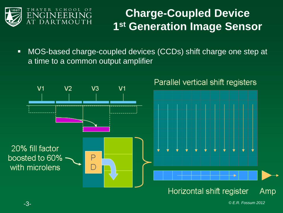
Charge-Coupled Device 1st Generation Image Sensor
MOS-based charge-coupled devices (CCDs) shift charge one step at a time to a common output amplifier

-4- © E.R. Fossum 2012
CCD Limitations
Requires high charge transfer efficiency Special fabrication process adds cost Larger voltage swings, different voltage levels
Difficult to integrate on-chip timing, control, drive and signal chain electronics Process integration increases cost, reduces yield Large capacitances require high current levels
Requires timing generator chip, driver chips, signal processor, ADC and interface chips
System power in 0.5-2 Watt range Architecture yields serial access to image data Limited frame rates

-5- © E.R. Fossum 2012
CMOS Active Pixel Sensor 2nd Generation Image Sensor
Pain et al. 2007 IISW
Camera on a Chip
Active pixel array
Analog signal chain
Analog-to-Digital Conv.
VLSI Digital logic
I/O interface
Timing and control
Exposure control
Color processing
Ancillary circuits
-6- © E.R. Fossum 2012
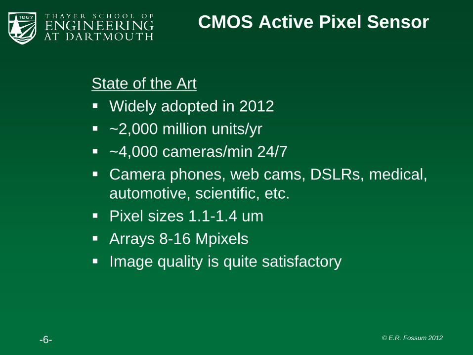
CMOS Active Pixel Sensor
State of the Art Widely adopted in 2012 ~2,000 million units/yr ~4,000 cameras/min 24/7 Camera phones, web cams, DSLRs, medical,
automotive, scientific, etc. Pixel sizes 1.1-1.4 um Arrays 8-16 Mpixels Image quality is quite satisfactory

-7- © E.R. Fossum 2012
From the Late 1990’s
1970 1980 1990 2000
CCDs
APS
Sys
tem
Cos
t/Per
form
ance
2010
QIS?

-8- © E.R. Fossum 2012
Future Mainstream CMOS Characteristics
Use of nanometer-scale nodes e.g. 22 −> 14 nm
Lower operating voltages 0.8 −> 0.4 volts
Use of materials other than silicon e.g. such as graphene, SiGe, or InGaAs on silicon
Use of 3D gates structures Tri-gate or finFET
All of these trends are problematic for CMOS APS

-9- © E.R. Fossum 2012
Reduction in Operating Voltage
In 1994 we thought it was a great challenge to make a pinned photodiode operate with a 5V swing. What about 0.5 volt swing?
Noise reduction has, in part, been accomplished with higher conversion gain, but this requires larger rail voltages to achieve the same full well. 10k e- full well at 100 uV/e- requires 1 volt swing
Analog signal chain much easier at 1 volt rail-to-rail, or higher.

-10- © E.R. Fossum 2012
Charge storage in buried or pinned photodiode
Krymski, 2005 IISW
• No Si-SiO2 interfaces, low trapping and generation • All silicon, well gettered, few defects • Diffusion-limited dark current • Complete charge transfer for readout • “Large” structure, must store full well signal.

-11- © E.R. Fossum 2012
Digital Integration Sensor
Can relieve issues with pinned photodiode capacity, readout electronics full well capacity, and improve dynamic range.
Deliberately make full well capacity much smaller in pinned photodiode (easier design and process)
Use higher conversion gain to improve read noise (reduced FD area and capacitance)
Add successive fast frames in digital memory.
See Hynecek US Patent No. 7,825,971 and Patent Applications by Fossum 2011

-12- © E.R. Fossum 2012
Digital Integration Sensor (DIS)
Σ Memory
time
• Break into multiple sub-integration periods
• Exposure sub-integration times can be varied to increase dynamic range
• Frames can be shifted to remove motion blur
Conventional integration period
-13- © E.R. Fossum 2012
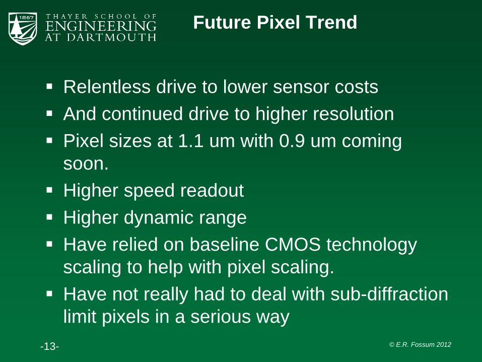
Future Pixel Trend
Relentless drive to lower sensor costs And continued drive to higher resolution Pixel sizes at 1.1 um with 0.9 um coming
soon. Higher speed readout Higher dynamic range Have relied on baseline CMOS technology
scaling to help with pixel scaling. Have not really had to deal with sub-diffraction
limit pixels in a serious way
-14- © E.R. Fossum 2012
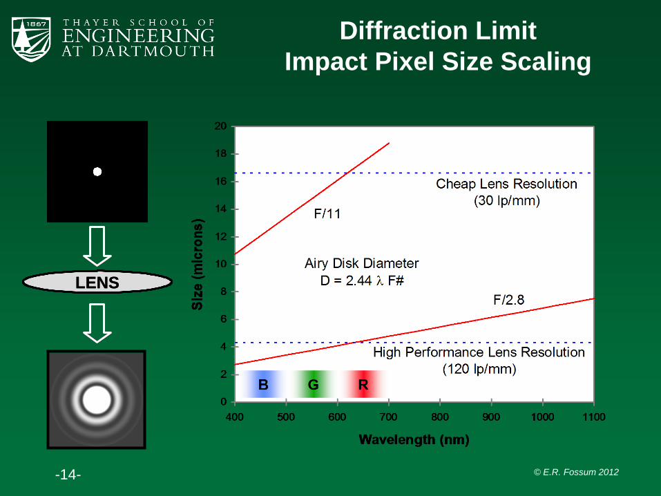
Diffraction Limit Impact Pixel Size Scaling
LENS LENS LENS

-15- © E.R. Fossum 2012
Sub-Diffraction Limit Pixels
0.9 um pixel pitch • Marginal return on shrink for real resolution improvement • Sort of a spatial and color oversampling • Anti-aliasing filter not needed
• Some real limit on how small is practical according to current pixel paradigm
• Could possibly remove diffraction effect by ISP but would probably reduce SNR
-16- © E.R. Fossum 2012
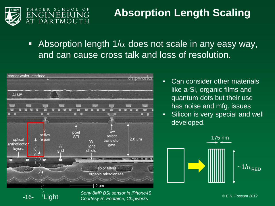
Absorption Length Scaling
Absorption length 1/α does not scale in any easy way, and can cause cross talk and loss of resolution.
Light
175 nm
~1/αRED
• Can consider other materials like a-Si, organic films and quantum dots but their use has noise and mfg. issues
• Silicon is very special and well developed.
Sony 8MP BSI sensor in iPhone4S Courtesy R. Fontaine, Chipworks

-17- © E.R. Fossum 2012
Baseline CMOS processes evolving
M. Bohr, 2011 IEDM

-18- © E.R. Fossum 2012
Time for a Paradigm Shift?
Current paradigm: We collect photons for a
predetermined amount of time in a silicon “rainbucket” determined by physical size and capacity of silicon pixel.
New paradigm: Let’s count each
photogenerated carrier and record time and location, creating binary bit planes for each time slice, and then digitally form image by digital convolution over X,Y, t.
x
y
Image pixel

-19- © E.R. Fossum 2012
QIS Concept
A Quanta Image Sensor (QIS) is an array of specialized photon-counting pixels called jots.
A QIS might contain 1-100 Gjots.
A QIS is read out 250-1000 times per second.
A QIS generates about 0.25- 100 Tbits/sec data rate.
The Tbit/sec data can be processed on-chip and off-chip to form an image.

-20- © E.R. Fossum 2012
Core QIS Architecture
TIM
ING
AN
D
RO
W D
RIV
ER
S JOT ARRAY
COLUMN SENSE AMPLIFIERS
ROW SCAN

-21- © E.R. Fossum 2012
TDI, Motion Deblur and Wavefront Correction
• Shift successive frames based on known scan direction, image-based motion flow or guide star

-22- © E.R. Fossum 2012
Related Prior Art
Solid-State Photon Counting in Visible (Low noise, big pixels) Image intensified image sensors (CCD and CMOS APS) Electron multiplying CCDs (internal avalanche) Single photon avalanche detectors (SPADs) Nano-multiplication-region avalanche photodiode (NAPD) Amplified pixels with sub-electron read noise.
Binary Pixels using DRAM (Threshold detectors, small pixels) Micron “eye” Gigavision camera
Digital Pixels (Analog pixel, digitize and count in or near pixel) Digital pixel sensor (DPS) NHK Digital image sensor
Image Stabilization and HDR “Anti-shake” by adding high-speed frames offset from one another High dynamic range by merging 2-3 differently exposed frames “Lucky” imaging in astronomy

-23- © E.R. Fossum 2012
Jot
A jot is an nano-scale active pixel with binary output sensitive to a single photocarrier
Takes many jots (space and/or time) to make an image pixel.
Jot Functionality 1. Photodetector 2. High gain 3. Select/drive 4. Reset Could be merged to one or two devices
per jot
Functional illustration only

-24- © E.R. Fossum 2012
Jot Implementation
There are several avenues for jot implementation. 1. Brute force scale-down of CMOS active pixel
sensor. Read noise must be reduced. Achieving required dimensions challenging.
2. Modify a SPAD or NAPD device for QIS application. 3. Single-electron field effect transistor (SEFET). One
electron causes enough current change to be detected by column sense amplifiers.
4. Stacked device (e.g. using SixGe1-x ) 5. New device to-be-invented based on quantum dot
film or other nanoscale device.

-25- © E.R. Fossum 2012
CMOS APS SOA at about 900 nm pixel
Light
Front side of wafer
Example from Sony Pixel Trend From TSMC

-26- © E.R. Fossum 2012
CMOS APS Jot
Requires shrink from 900 nm to 200-100 nm scale. About 20-80 x decrease in pixel area.
Requires increase in conversion gain of about 200x. (50 uV/e- -> 10 mV/e-)
Requires decrease in input-referred read noise of about 20x from 3 e- rms -> 0.15 e-
Requires decrease in full well from 3000 e- to 1-10 e- (this part is easy).
* Note that future sub-electron read noise in CMOS APS can lead to photon counting, which at low counts is like a multi-level jot, albeit not a pure jot.

-27- © E.R. Fossum 2012
Example of SPAD SOA
2011 IISW

-28- © E.R. Fossum 2012
Modified SPAD
SPAD size must be reduced from ~5000 nm pitch to 200-100 nm (about 600-2500x change in pixel area).
Can eliminate SPAD timer circuitry. Replace continuous time circuitry with
read/reset select-activated circuitry. Increase SPAD count from 32x32 (1024
elements) more than one million fold.

-29- © E.R. Fossum 2012
Samsung
Status: • TCAD model only • Shows about 5-10 mV/e- signal • More work required
SEFET - Single Electron Field Effect Transistor

-30- © E.R. Fossum 2012
Total Equiv. Data Rate
Total equiv. data rate Q = Npix x Nfw x F where Npix = number of pixels, Nfw = full well, and F=frame rate For sCMOS, Npix = 5.5x10⁶, Nfw = 2x16,000, F=30 Equiv data rate Q = 5.3 Tb/s (We ignore the chance that a jot captures more than one carrier which
is not a good assumption near saturation.)

-31- © E.R. Fossum 2012
Pixels to Jots
6500 nm pixel pitch Say, 100 nm jot pitch, or 65x65 jots per pixel At saturation, this is 4,225 electrons For Nfw of 31,700, need 8 of these = 33,800 Jot field rate is 8x pixel frame rate = 240 fps. Pixels 2,560H x 2,160V = 5.5 Mpixels x 65H x 65V
Jots 166,400H x 140,400V = 23.4 Gjots 23.4 Gjots x 8 x 30fps = 5.6 Tb/s Column scan rate (down column) is 140,400V x 240 fps = 33.7 MHz
1 pixel 4,225 jots

-32- © E.R. Fossum 2012
Pixels to Jots Data Rates
Sensor sCMOS Aptina 8M sCMOS Aptina 8M
Pixel Pitch (nm) 6500 1400 6500 1400Pixels H 2560 3264 2560 3264Pixels V 2160 2448 2160 2448
Total (Mpix) 5.5 8.0 5.5 8.0
Full Well (e-) 31700 3000 31700 3000Frame Rate (Hz) 30 15 30 15
Te-/sec 5.3 0.4 5.3 0.4
Jot Pitch (nm) 100 100 200 200Jots/Pixel 4225 196 1056 49
Jots H 166400 45696 83200 22848Jots V 140400 34272 70200 17136
Total (Gjot) 23.4 1.6 5.8 0.4
e-/jot/frame 7.5 15.3 30.0 61.2Bit plane readout (Hz) 225.1 229.6 900.4 918.4
Column scan rate (MHz) 31.6 7.9 63.2 15.7
Total jot rate (Tb/sec) 5.3 0.4 5.3 0.4
After KP (Gb/s) 1.2 1.8 5.0 7.3
-33- © E.R. Fossum 2012
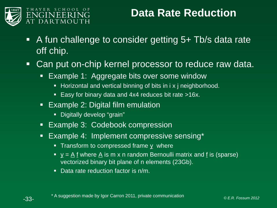
Data Rate Reduction
A fun challenge to consider getting 5+ Tb/s data rate off chip.
Can put on-chip kernel processor to reduce raw data. Example 1: Aggregate bits over some window
Horizontal and vertical binning of bits in i x j neighborhood. Easy for binary data and 4x4 reduces bit rate >16x.
Example 2: Digital film emulation Digitally develop “grain”
Example 3: Codebook compression Example 4: Implement compressive sensing*
Transform to compressed frame y where y = A f where A is m x n random Bernoulli matrix and f is (sparse)
vectorized binary bit plane of n elements (23Gb). Data rate reduction factor is n/m.
* A suggestion made by Igor Carron 2011, private communication

-34- © E.R. Fossum 2012
QIS Planar Architecture
JOT ARRAY
COLUMN SENSE AMPLIFIERS
ACCUMULATING LOGIC+MEMORY
KERNEL PROCESSOR
OUTPUT MULTIPLEXER
RO
W D
RIV
ER
S
TIM
ING
AN
D
CO
NTR
OL
OFF CHIP MEMORY + IMAGE FORMATION PROCESSOR
BIT PLANE DATA
n x n AGGREGATION ON-CHIP PROCESSOR
PROGRAM
READ POINTER
RESET POINTER APERTURE QUANTA
IMAGE SENSOR
(QIS)
TEMPORAL AGGREGATION

-35- © E.R. Fossum 2012
Why Work on QIS Technology?
IDEALISM: Counting photon strikes “without” read noise is nearly ideal. (Measuring energy would be even better.) Photon counting keeps quantized light in the quantized (bit) domain
ALIGNMENT: Future nanoelectronics (e.g. graphene technology) may not allow integration of photocarriers within the semiconductor.
TIMING: Soon, mainstream microelectronics technology will enable realization of a QIS.
IMAGING PERFORMANCE: QIS puts most analog signal processing into the digital domain at the earliest
opportunity taking advantage of improvements and the flexibility of digital signal processing.
Improved low light imaging. Improved tracking of targets in space and time TDI in any scan direction Time-resolved scientific low-light imaging with high resolution Emulation of different image formation processes easily achieved, such as
“digital film”
-36- © E.R. Fossum 2012
New Research Activities
Application studies Architectural studies Development of jot device(s) Signal chain On-chip kernel processor Off-chip image formation algorithms Power management Noise shaping and other digital signal processing
algorithms. End to end system simulation Work started in several areas at Dartmouth
-37- © E.R. Fossum 2012
Conclusions
Quanta Image Sensor (QIS) “vision” is to count every photon that hits the sensor, recording its location and arrival time, and create pixels from bit-planes of data
QIS driven by at least four factors Pixel shrink runs into full well capacity issues. Optical resolution limited by diffraction limit Strong drive to sub-electron read noise Future CMOS processes may not be well aligned to CMOS
APS needs and trends. QIS is a paradigm shift in the way we do imaging Too early to tell if this will have a compelling
advantage for consumer electronics, but looks promising for scientific and aerospace apps.
We are at the beginning.


![IMAGE RECONSTRUCTION FOR QUANTA IMAGE SENSORS USING … · INTRODUCTION Quanta Image Sensor (QIS) is a new type of image sensor envisioned to supersede CMOS and CCD [1]. Having a](https://img.pdfslide.us/doc/110x75/601b455bae2e7d65d15541ff/image-reconstruction-for-quanta-image-sensors-using-introduction-quanta-image-sensor.jpg)