Embed Size (px)
Citation preview
Quad Pin Timing Formatter ADATE207
Rev. 0 Information furnished by Analog Devices is believed to be accurate and reliable. However, no responsibility is assumed by Analog Devices for its use, nor for any infringements of patents or other rights of third parties that may result from its use. Specifications subject to change without notice. No license is granted by implication or otherwise under any patent or patent rights of Analog Devices. Trademarks and registered trademarks are the property of their respective owners.
One Technology Way, P.O. Box 9106, Norwood, MA 02062-9106, U.S.A.Tel: 781.329.4700 www.analog.com Fax: 781.461.3113 ©2007 Analog Devices, Inc. All rights reserved.
FEATURES 4-channel timing formatter 256 waveforms per channel 4 independent event edges per waveform STIL IEEE 1450-1999-compatible events 4-period range for each edge 39.06 ps timing resolution 2.5 ns minimum edge refire rate All drive formats supported 100 MHz base vector rate ×2 and ×4 high speed modes ×2 pin multiplexing 1 ns minimum pulse width 32-bit fail counter per channel 4-bit pin capture per channel Air cooled, low power CMOS design 6 W at 100 MHz base rate 2.5 V power supply Differential DCL interface control TMU multiplexer
APPLICATIONS Automatic test equipment (ATE) High speed digital instrumentation Pulse generation
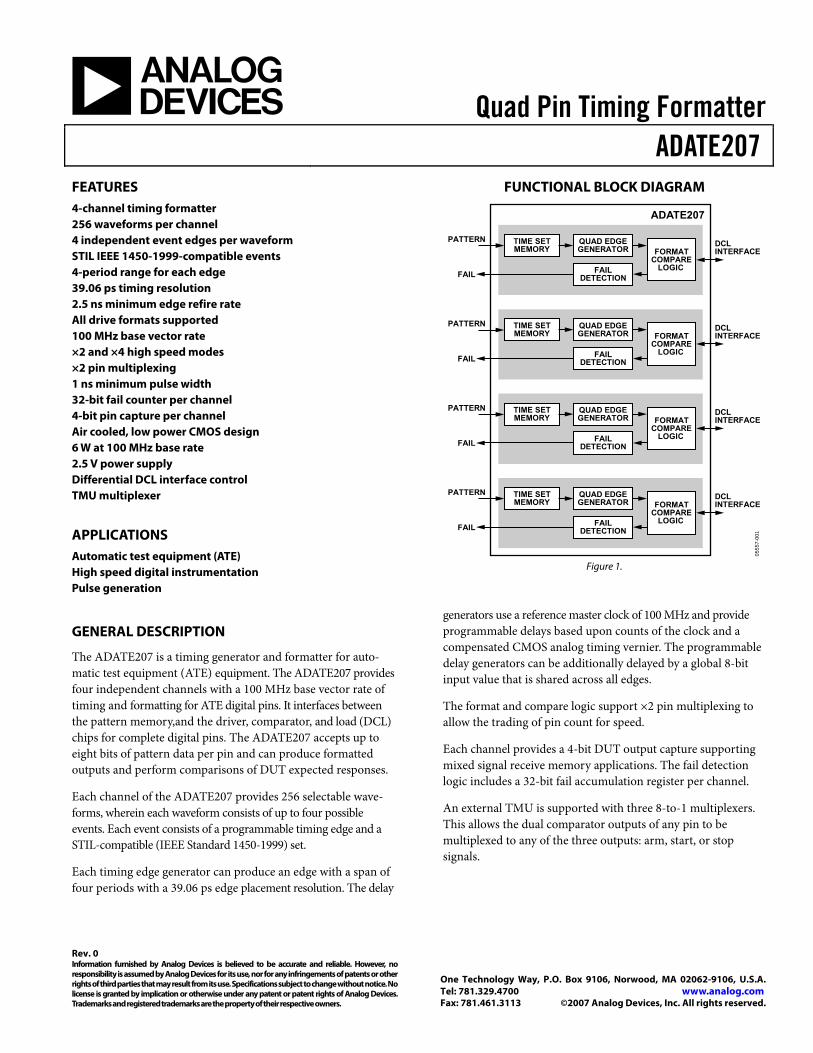
FUNCTIONAL BLOCK DIAGRAM
TIME SETMEMORY FORMAT
COMPARELOGIC
QUAD EDGEGENERATOR
FAILDETECTION
PATTERN
FAIL
DCLINTERFACE
TIME SETMEMORY FORMAT
COMPARELOGIC
QUAD EDGEGENERATOR
FAILDETECTION
PATTERN
FAIL
DCLINTERFACE
TIME SETMEMORY FORMAT
COMPARELOGIC
QUAD EDGEGENERATOR
FAILDETECTION
PATTERN
FAIL
DCLINTERFACE
TIME SETMEMORY FORMAT
COMPARELOGIC
QUAD EDGEGENERATOR
FAILDETECTION
PATTERN
FAIL
DCLINTERFACE
ADATE207
0555
7-00
1
Figure 1.
GENERAL DESCRIPTION
The ADATE207 is a timing generator and formatter for auto-matic test equipment (ATE) equipment. The ADATE207 provides four independent channels with a 100 MHz base vector rate of timing and formatting for ATE digital pins. It interfaces between the pattern memory,and the driver, comparator, and load (DCL) chips for complete digital pins. The ADATE207 accepts up to eight bits of pattern data per pin and can produce formatted outputs and perform comparisons of DUT expected responses.
Each channel of the ADATE207 provides 256 selectable wave-forms, wherein each waveform consists of up to four possible events. Each event consists of a programmable timing edge and a STIL-compatible (IEEE Standard 1450-1999) set.
Each timing edge generator can produce an edge with a span of four periods with a 39.06 ps edge placement resolution. The delay
generators use a reference master clock of 100 MHz and provide programmable delays based upon counts of the clock and a compensated CMOS analog timing vernier. The programmable delay generators can be additionally delayed by a global 8-bit input value that is shared across all edges.
The format and compare logic support ×2 pin multiplexing to allow the trading of pin count for speed.
Each channel provides a 4-bit DUT output capture supporting mixed signal receive memory applications. The fail detection logic includes a 32-bit fail accumulation register per channel.
An external TMU is supported with three 8-to-1 multiplexers. This allows the dual comparator outputs of any pin to be multiplexed to any of the three outputs: arm, start, or stop signals.
ADATE207
Rev. 0 | Page 2 of 36
TABLE OF CONTENTS Features .............................................................................................. 1
Applications....................................................................................... 1
Functional Block Diagram .............................................................. 1
General Description ......................................................................... 1
Specifications..................................................................................... 3
DC Specifications ......................................................................... 3
AC Specifications.......................................................................... 4
Timing Diagrams.......................................................................... 5
Absolute Maximum Ratings............................................................ 6
Thermal Resistance ...................................................................... 6
Bypassing Scheme ........................................................................ 6
ESD Caution.................................................................................. 6
Pin Configurations and Function Descriptions ........................... 7
Theory of Operation ...................................................................... 12
Waveform Memory .................................................................... 12
Event Generators ........................................................................ 12
Delay Generation........................................................................ 12
Vernier Resolution ..................................................................... 12
Drive and Compare Logic......................................................... 13
Pipeline Considerations............................................................. 14
DUT Capture .............................................................................. 15
TMU Multiplexer ....................................................................... 15
Low Jitter Clock Driver ............................................................. 15
Clock Generator Mode .............................................................. 15
Device Reset ................................................................................ 15
Temperature Diode .................................................................... 17
High Speed Differential DCL Interface................................... 17
Control and Status Register Interface .......................................... 18
Read/Write Function ................................................................. 18
Control and Status Registers ......................................................... 21
Channel Specific and Common Registers .............................. 22
Chip-Specific (Common) Registers......................................... 30
Application Information ............................................................... 34
Time Measurement Support ..................................................... 34
Outline Dimensions ....................................................................... 35
Ordering Guide .......................................................................... 35
REVISION HISTORY
5/07—Revision 0: Initial Version
ADATE207
Rev. 0 | Page 3 of 36
SPECIFICATIONS DC SPECIFICATIONS TC = 85°C ± 5°C, VDD = 2.5 V, unless otherwise noted.
Table 1. Parameter Conditions Min Typ Max Unit POWER SUPPLY
Operating Supply Current, IDD All channels repeating pattern of 1/H/0/L across D0/D1/D2/D3 edges every 20 ns
2.5 2.7 A
Power Dissipation1 All channels repeating pattern of 1/H/0/L across D0/D1/D2/D3 edges every 20 ns
6.3 7.1 W
All channels repeating pattern of H/L/H/L across D0/D1/D2/D3 edges every 10 ns
6.85 W
Idle mode; no patterns bursting 5.7 W Operating Supply Current, IDD All channels repeating pattern of 1/0/1/0 across
D0/D1/D2/D3 edges every 10 ns 2.7 A
Idle mode; no patterns bursting 2.2 A DIGITAL INPUTS
LVCMOS25 VIL 0.7 V IIL VIL = 0 V 1 μA VIH 1.7 V IIH VIH = 2.5 V 1 μA Pin Capacitance Guaranteed by simulation 3.5 pF
Differential Inputs with Internal Termination
VDIFF 200 mV Input Voltage Range 1.0 VDD V
Differential inputs with External Termination
VDIFF 200 mV Input Voltage Range 1.0 VDD V R Termination 50 ± 15% Ω
DIGITAL BIDIRECTIONALS LVCMOS25
VIL 0.7 V IIL VIL = 0 V 1 μA VIH 1.7 V IIH VIH = 2.5 V 1 μA
DIGITAL OUTPUTS LVCMOS25
VOL IOL = 8 mA 0.4 V VOH IOH = 8 mA VDD − 0.4 V
Open Drain Differential Outputs REF_1K > 100 kΩ to GND VDIFF VTERM = 50 Ω to VDD 200 300 mV VOL (Individual Leg of Pair) VTERM = 50 Ω to VDD 2.49 V VOH (Individual Leg of Pair) VTERM = 50 Ω to VDD 2.2 V
Ambient Potential IDIODE = 100 μA 715 mV Operating Potential IDIODE = 100 μA 600 630 mV Temperature Coefficient IDIODE = 100 μA 1.4 mV/°C
1 Power dissipation specifically indicates part dissipation and does not include power dissipated in external terminations.

ADATE207
Rev. 0 | Page 4 of 36
AC SPECIFICATIONS TC = 85°C ± 5°C, VDD = 2.5 V, unless otherwise noted.
Table 2. Parameter Conditions Min Typ Max Unit CLOCK INPUTS
Master Clock (MCLK) Frequency 100 MHz MCLK Duty Cycle 46 50 54 %
DRIVE OUTPUTS Output Pulse Width Timing error < ±125 ps 1 ns
COMPARE INPUTS Minimum Comparison Window Width 1.25 ns Minimum Detectable Glitch Width 1.25 ns
EDGE PERFORMANCE Retrigger Time 2.5 ns Edge Delay 0 Lesser of 4 T0 cycles
or 163.8 μs
Vernier Resolution 39.06 ps Vernier Timing DNL −150 +150 ps Vernier Timing INL −150 +150 ps Vernier Temperature Coefficient 4 ps/°C Edge Jitter MCLK jitter 5 ps rms 20 ps rms
CONTROL AND STATUS REGISTER (CSR) INTERFACE Clock Period 10 ns Setup Time (tBSU) MCLK 1.1 ns Hold Time (tBH) MCLK 0.5 ns Clock to Output (tBCO) MCLK 2.5 7.0 ns Clock to Tristate (tBCZ) 2.3 4.2 ns Clock to Data Valid from Tristate (tBCZV) 0 7.0 ns
DIGITAL INPUTS Set Up (tISU) MCLK 1.7 ns Hold Time (tIH) MCLK 0.5 ns
DIGITAL OUTPUTS Clock to Output (tOCO) MCLK 0.7 1.6 ns
JTAG PORTS JTAG Clock Period 100 ns Setup Time (tSSU) JTAG CLOCK 50 ns Hold Time (tSH) JTAG CLOCK 50 ns Clock to Output (tSCO) JTAG CLOCK 50 ns

ADATE207
Rev. 0 | Page 5 of 36
TIMING DIAGRAMS
tISU tIH
MCLK_P
DIGITAL INPUTS
MCLK_N
DIGITAL OUTPUTS
tOCO(MIN)
tOCO(MAX)
0555
7-00
7
Figure 2. Timing Diagram for Inputs and Outputs
tJSU tJH
JTAG
JTAG INPUT
JTAG OUTPUT
tJCO
0555
7-01
5
Figure 3. Timing Diagram for Scan Inputs and Scan Outputs
tBSU tBH
MCLK_P
BIDIRECTIONAL (WRITES)
MCLK_N
BIDIRECTIONAL (READS)
tBCO(MIN)
tBCO(MAX)
tBCZ
tBCZV
0555
7-00
8
Figure 4. Timing Diagram for Bidirectional Reads and Writes

ADATE207
Rev. 0 | Page 6 of 36
ABSOLUTE MAXIMUM RATINGS Table 3. Parameter Rating VDD −0.3 V to +2.8 V Digital Inputs −0.3 V to VDD + 0.3 V Resistor Termination pins −0.3 to VDD + 0.3 V Resistor Termination Current 12 mA max Termination Pad Current 12 mA max Junction Temperature 125°C Storage Temperature −40 to 125°C
Stresses above those listed under Absolute Maximum Ratings may cause permanent damage to the device. This is a stress rating only; functional operation of the device at these or any other conditions above those indicated in the operational section of this specification is not implied. Exposure to absolute maximum rating conditions for extended periods may affect device reliability.
Table 4. Recommended Operating/Environmental Conditions Parameter Min Typ Max Unit VDD 2.375 2.5 2.625 V Case Temperature (TC) 85 °C Relative Humidity (Noncondensing)
85 %
THERMAL RESISTANCE Table 5. Thermal Resistance Package Type θJA θJC Unit 256-Lead BGA_ED 1.5 °C/W
In Still Air 14.3 °C/W 200 LFPM 12.0 °C/W 400 LFPM 11.2 °C/W
BYPASSING SCHEME For decoupling, best practice suggests that to preserve as much of the plane-to-plane capacitance as possible, do not perforate the planes for VSS and VDD. Secondly, it is advisable to decouple VDD to VSS by using 0.1 μF high frequency ceramic capacitors. The trace to the capacitor should be kept to an absolute minimum length. It is recommend that one capacitor be placed in the corner of the chip and one in the middle of each side for a total of eight capacitors for VDD to VSS. Furthermore, decouple IOVDD to IOVSS on each side of the device. It is recommended that 10 μF tantalum or ceramic capacitors be used for low frequency decoupling around the device. It is not important for these capacitors to be close to the device.
Table 6. Data Table for 256-Lead Ball Grid Array, Thermally Enhanced, 27 mm × 27 mm Body
Dimension Minimum (mm)
Nominal (mm)
Maximum (mm)
A 1.70
A1 0.50 0.60 0.70 A2 0.60 0.80 1.00 D 26.90 27.00 27.10 D1 24.03 24.13 24.23 E 26.90 27.00 27.10 E1 24.03 24.13 24.23 b 0.60 0.75 0.90 e 1.27 aaa 0.20 bbb 0.25 ccc 0.35 ddd 0.20 eee 0.30 fff 0.15 S 0.635
ESD CAUTION

ADATE207
Rev. 0 | Page 7 of 36
PIN CONFIGURATIONS AND FUNCTION DESCRIPTIONS
ADATE207
PATTERN DATA
PERIOD DATA
COMPARE FAILS
RECEIVE DATACH3 DCL I/F
CH2 DCL I/F
CH1 DCL I/F
CH0 DCL I/F
COMMAND/STATUS BUS
TIMEMEASUREMENT 05
557-
009
Figure 5. Connection Overview Diagram
ABCDEFGHJKLMNPRTUVWY
2468101214161820135791113151719
BOTTOMVIEW
(Not to Scale)
ADATE207
0555
7-01
4
Figure 6. Ball Grid Array
Table 7. Pin Function Descriptions Pin No. Mnemonic Input/Output1 Type Description B4, A4, C5, D6 PAT_MASK[3:0] I LVCMOS25 Mask Failures. Used to mask failures on D3,
D2, D1 and D0 edges, respectively. Clocked by MCLK.
T3, U1, U2, T4, U3, V4, U5, W4 PAT_PATDATA_0[7:0] I LVCMOS25 Channel 0 Waveform Memory Address. Use these pins to address waveform memory for Channel 0. Clocked by MCLK.
B5, A5, C6, B6, A6, C7, B7, D8 PAT_PATDATA_1[7:0] I LVCMOS25 Channel 1 Waveform Memory Address. Use these pins to address waveform memory for Channel 1. Clocked by MCLK.
W212, V12, Y13, U12, W13, V13, Y14, W14
PAT_PATDATA_2[7:0] I LVCMOS25 Channel 2 Waveform Memory Address. Use these pins to address waveform memory for Channel 2. Clocked by MCLK.
A16, B16, D15, C16, A17, B17, D16, C17
PAT_PATDATA_3[7:0] I LVCMOS25 Channel 3 Waveform Memory Address. Use these pins to address waveform memory for Channel 3. Clocked by MCLK.
Y4, W5, V6 PAT_FAIL_0[3:0] O LVCMOS25 Fails on D3, D2, D1 and D0 Edges for Channel 0. Clocked by MCLK.
B8, A8, B9, B10 PAT_FAIL_1[3:0] O LVCMOS25 Fails on D3, D2, D1 and D0 Edges for Channel 1. Clocked by MCLK.
V8, W8, W9, Y9 PAT_FAIL_2[3:0] O LVCMOS25 Fails on D3, D2, D1 and D0 Edges for Channel 2. Clocked by MCLK.
B12, C12, B13, A14 PAT_FAIL_3[3:0] O LVCMOS25 Fails on D3, D2, D1 and D0 Edges for Channel 3. Clocked by MCLK.
W6, Y6, W7, Y7 PAT_DUTDATA_0[3:0] O LVCMOS25 DUT Capture Data from Channel 0. Clocked by MCLK.
C10, A11, B11, A12 PAT_DUTDATA_1[3:0] O LVCMOS25 DUT Capture Data from Channel 1. Clocked by MCLK.
V10, W10, Y10, W11 PAT_DUTDATA_2[3:0] O LVCMOS25 DUT Capture Data from Channel 2. Clocked by MCLK.
B14, C14, A15, B15 PAT_DUTDATA_3[3:0] O LVCMOS25 DUT Capture Data from Channel 3. Clocked by MCLK.

ADATE207
Rev. 0 | Page 8 of 36
Pin No. Mnemonic Input/Output1 Type Description D5 PAT_DATA_VALID I LVCMOS25 Indicates Pattern Bursting. When not
asserted, edges are disabled and the drive and expect signals are static. Clocked by MCLK.
F3 PER_EARLY_T0EN I LVCMOS25 Indicates the Start of a T0 Period. Clocked by MCLK.
E1 PER_EARLY_C0EN I LVCMOS25 Indicates the Start of a C0 Period. Clocked by MCLK.
C4, D3, E4, D2, D1, E3, F4, E2 INPUT_DELAY[7:0] I LVCMOS25 Global Delay Input For All Edges. Clocked by MCLK.
F18 TMU_ARM_P D, O Differential open-drain
Differential Tristate Output. Noninverted TMU ARM multiplexer output. High-Z when not enabled.
E20 TMU_ARM_N D, O Differential open-drain
Differential Tristate Output. Inverted TMU ARM multiplexer output. High-Z when not enabled.
E19 TMU_START_P D, O Differential open-drain
Differential Tristate Output. Noninverted TMU START multiplexer output. High-Z when not enabled.
F17 TMU_START_N D, O Differential open-drain
Differential Tristate Output. Inverted TMU START multiplexer output. High-Z when not enabled.
E18 TMU_STOP_P D, O Differential open-drain
Noninverted TMU STOP Multiplexer Output. Differential tristate output. High-Z when not enabled.
D20 TMU_STOP_N D, O Differential open-drain
Inverted TMU STOP Multiplexer Output. Differential tristate output. High-Z when not enabled.
P2 DR_DATA_CH0_P D, O Differential open-drain
Noninverted DCL Drive Data Signal for Channel 0.
P1 DR_DATA_CH0_N D, O Differential open-drain
Inverted DCL Drive Data Signal for Channel 0.
G3 DR_DATA_CH1_P D, O Differential open-drain
Noninverted DCL Drive Data Signal for Channel 1.
H4 DR_DATA_CH1_N D, O Differential open-drain
Inverted DCL Drive Data Signal for Channel 1.
P19 DR_DATA_CH2_P D, O Differential open-drain
Noninverted DCL Drive Data Signal for Channel 2.
P20 DR_DATA_CH2_N DO Differential open-drain
Inverted DCL Drive Data Signal for Channel 2.
G18 DR_DATA_CH3_P D, O Differential open-drain
Noninverted DCL Drive Data Signal for Channel 3.
H17 DR_DATA_CH3_N D, O Differential open-drain
Inverted DCL Drive Data Signal for Channel 3.
N3 DR_EN_CH0_P D, O Differential open-drain
Noninverted DCL Drive Enable Signal for Channel 0.
N2 DR_EN_CH0_N D, O Differential open-drain
Inverted DCL Drive Enable Signal for Channel 0.
G2 DR_EN_CH1_P D, O Differential open-drain
Noninverted DCL Drive Enable Signal for Channel 1.
G1 DR_EN_CH1_N D, O Differential open-drain
Inverted DCL Drive Enable Signal for Channel 1.
N18 DR_EN_CH2_P D, O Differential open-drain
Noninverted DCL Drive Enable Signal for Channel 2.
N19 DR_EN_CH2_N D, O Differential open-drain
Inverted DCL Drive Enable Signal for Channel 2.
G19 DR_EN_CH3_P D, O Differential open-drain
Noninverted DCL Drive Enable Signal for Channel 3.
ADATE207
Rev. 0 | Page 9 of 36
Pin No. Mnemonic Input/Output1 Type Description G20 DR_EN_CH3_N D, O Differential
open-drain Inverted DCL Drive Enable Signal for Channel 3.
L20 LJ_CLK_P D, I Differential input
Noninverted Low Jitter Clock Input. This pin can be multiplexed onto DR_DATA outputs for Channel 2 and Channel 3.
K19 LJ_CLK_N D, I Differential Input
Inverted Low Jitter Clock Input. This pin can be multiplexed onto DR_DATA outputs for Channel 2 and Channel 3.
M3 COMP_H_CH0_P D, I Differential input terminated
Noninverted DCL High Comparator Signal for Channel 0. Differential signal is Logic 1 when the DUT output is higher than VOH.
M2 COMP_H_CH0_N D, I Differential input terminated
Inverted DCL High Comparator Signal for Channel 0.
J4 COMP_H_CH1_P D, I Differential input terminated
Noninverted DCL High Comparator Signal for Channel 1. Differential signal is Logic 1 when the DUT output is higher than VOH.
J3 COMP_H_CH1_N D, I Differential input terminated
Inverted DCL High Comparator Signal for Channel 1.
M18 COMP_H_CH2_P D, I Differential input terminated
Noninverted DCL High Comparator Signal for Channel 2. Differential signal is Logic 1 when the DUT output is higher than VOH.
M19 COMP_H_CH2_N D, I Differential input terminated
Inverted DCL High Comparator Signal for Channel 2.
J17 COMP_H_CH3_P D, I Differential input terminated
Noninverted DCL High Comparator Signal for Channel 3. Differential signal is Logic 1 when the DUT output is higher than VOH.
J18 COMP_H_CH3_N D, I Differential input terminated
Inverted DCL High Comparator Signal for Channel 3.
L3 COMP_L_CH0_P D, I Differential input terminated
Noninverted DCL Low Comparator Signal for Channel 0. Differential signal is Logic 1 when the DUT output is higher than VOL.
L4 COMP_L_CH0_N D, I Differential input terminated
Inverted Low Comparator Signal for Channel 0.
H1 COMP_L_CH1_P D, I Differential input terminated
Noninverted DCL Low Comparator Signal for Channel 1. Differential signal is Logic 1 when the DUT output is higher than VOL.
J2 COMP_L_CH1_N D, I Differential input terminated
Inverted Low Comparator Signal for Channel 1.
L18 COMP_L_CH2_P D, I Differential input terminated
Noninverted DCL Low Comparator Signal for Channel 2. Differential signal is Logic 1 when the DUT output is higher than VOL.
L17 COMP_L_CH2_N D, I Differential Input terminated
Inverted Low Comparator Signal for Channel 2.
H20 COMP_L_CH3_P D, I Differential input terminated
Noninverted DCL Low Comparator Signal for Channel 3. Differential signal is Logic 1 when the DUT output is higher than VOL.
J19 COMP_L_CH3_N D, I Differential input terminated
Inverted Low Comparator Signal for Channel 3.
M1 COMP_L_CH0_T A, I, O Analog Center Tap. Center tap of two 50 Ω resistor terminations for the low comparator differential inputs of Channel 0.
ADATE207
Rev. 0 | Page 10 of 36
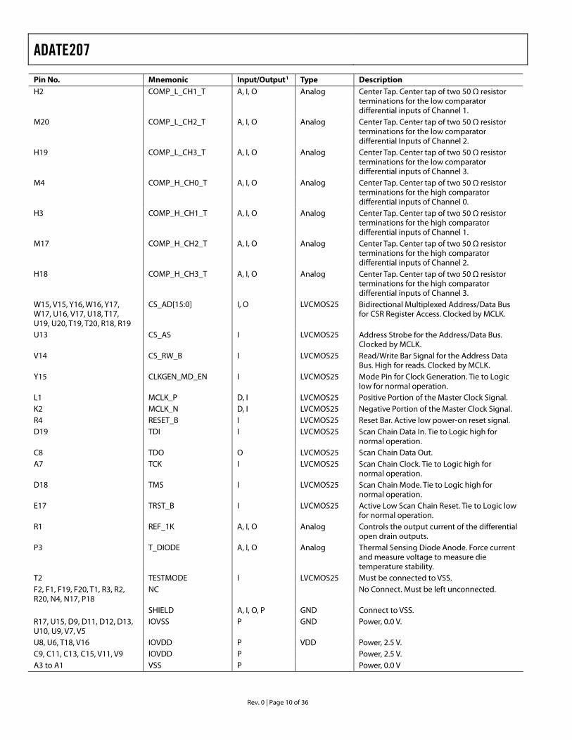
Pin No. Mnemonic Input/Output1 Type Description H2 COMP_L_CH1_T A, I, O Analog Center Tap. Center tap of two 50 Ω resistor
terminations for the low comparator differential inputs of Channel 1.
M20 COMP_L_CH2_T A, I, O Analog Center Tap. Center tap of two 50 Ω resistor terminations for the low comparator differential Inputs of Channel 2.
H19 COMP_L_CH3_T A, I, O Analog Center Tap. Center tap of two 50 Ω resistor terminations for the low comparator differential inputs of Channel 3.
M4 COMP_H_CH0_T A, I, O Analog Center Tap. Center tap of two 50 Ω resistor terminations for the high comparator differential inputs of Channel 0.
H3 COMP_H_CH1_T A, I, O Analog Center Tap. Center tap of two 50 Ω resistor terminations for the high comparator differential inputs of Channel 1.
M17 COMP_H_CH2_T A, I, O Analog Center Tap. Center tap of two 50 Ω resistor terminations for the high comparator differential inputs of Channel 2.
H18 COMP_H_CH3_T A, I, O Analog Center Tap. Center tap of two 50 Ω resistor terminations for the high comparator differential inputs of Channel 3.
W15, V15, Y16, W16, Y17, W17, U16, V17, U18, T17, U19, U20, T19, T20, R18, R19
CS_AD[15:0] I, O LVCMOS25 Bidirectional Multiplexed Address/Data Bus for CSR Register Access. Clocked by MCLK.
U13 CS_AS I LVCMOS25 Address Strobe for the Address/Data Bus. Clocked by MCLK.
V14 CS_RW_B I LVCMOS25 Read/Write Bar Signal for the Address Data Bus. High for reads. Clocked by MCLK.
Y15 CLKGEN_MD_EN I LVCMOS25 Mode Pin for Clock Generation. Tie to Logic low for normal operation.
L1 MCLK_P D, I LVCMOS25 Positive Portion of the Master Clock Signal. K2 MCLK_N D, I LVCMOS25 Negative Portion of the Master Clock Signal. R4 RESET_B I LVCMOS25 Reset Bar. Active low power-on reset signal. D19 TDI I LVCMOS25 Scan Chain Data In. Tie to Logic high for
normal operation. C8 TDO O LVCMOS25 Scan Chain Data Out. A7 TCK I LVCMOS25 Scan Chain Clock. Tie to Logic high for
normal operation. D18 TMS I LVCMOS25 Scan Chain Mode. Tie to Logic high for
normal operation. E17 TRST_B I LVCMOS25 Active Low Scan Chain Reset. Tie to Logic low
for normal operation. R1 REF_1K A, I, O Analog Controls the output current of the differential
open drain outputs. P3 T_DIODE A, I, O Analog Thermal Sensing Diode Anode. Force current
and measure voltage to measure die temperature stability.
T2 TESTMODE I LVCMOS25 Must be connected to VSS. F2, F1, F19, F20, T1, R3, R2, R20, N4, N17, P18
NC No Connect. Must be left unconnected.
SHIELD A, I, O, P GND Connect to VSS. R17, U15, D9, D11, D12, D13, U10, U9, V7, V5
IOVSS P GND Power, 0.0 V.
U8, U6, T18, V16 IOVDD P VDD Power, 2.5 V. C9, C11, C13, C15, V11, V9 IOVDD P Power, 2.5 V. A3 to A1 VSS P Power, 0.0 V
ADATE207
Rev. 0 | Page 11 of 36
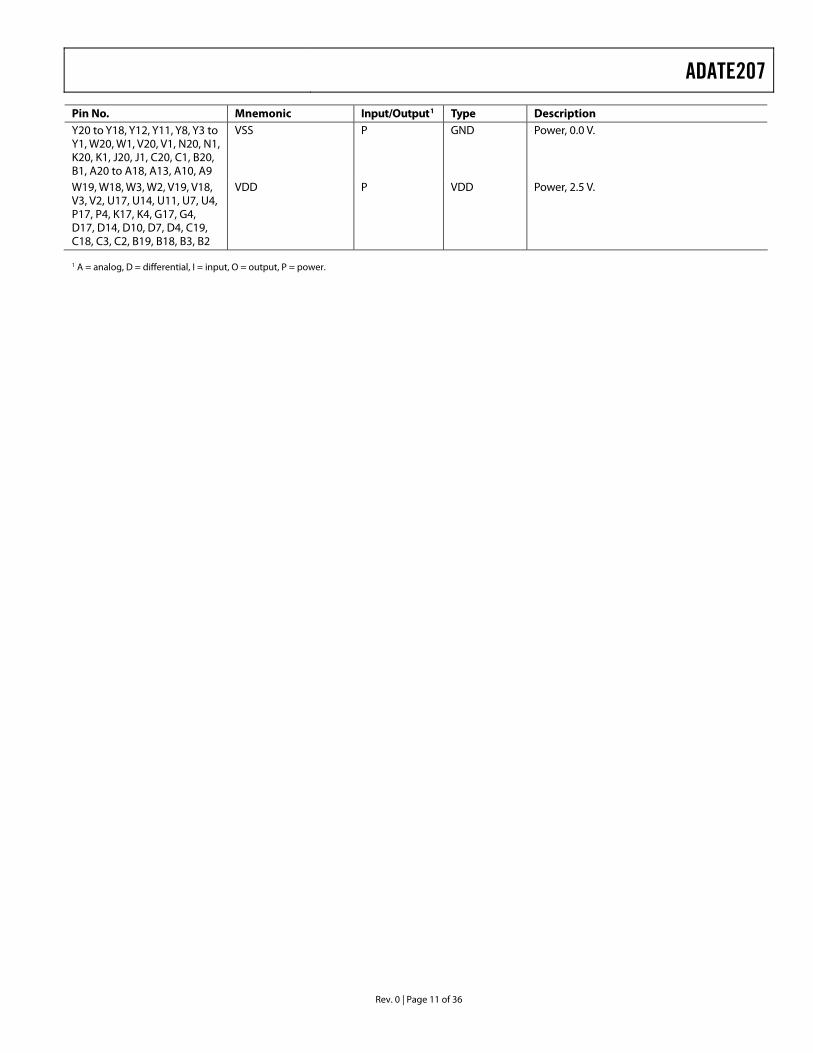
Pin No. Mnemonic Input/Output1 Type Description Y20 to Y18, Y12, Y11, Y8, Y3 to Y1, W20, W1, V20, V1, N20, N1, K20, K1, J20, J1, C20, C1, B20, B1, A20 to A18, A13, A10, A9
VSS P GND Power, 0.0 V.
W19, W18, W3, W2, V19, V18, V3, V2, U17, U14, U11, U7, U4, P17, P4, K17, K4, G17, G4, D17, D14, D10, D7, D4, C19, C18, C3, C2, B19, B18, B3, B2
VDD P VDD Power, 2.5 V.
1 A = analog, D = differential, I = input, O = output, P = power.
ADATE207
Rev. 0 | Page 12 of 36
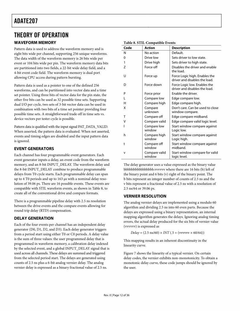
THEORY OF OPERATION WAVEFORM MEMORY Pattern data is used to address the waveform memory and is eight bits wide per channel, supporting 256 unique waveforms. The data width of the waveform memory is 26 bits wide per event or 104 bits wide per pin. The waveform memory data bits are partitioned into two fields, a 22-bit wide delay field, and a 4-bit event code field. The waveform memory is dual port allowing CPU access during pattern bursting.
Pattern data is used as a pointer to one of the defined 256 waveforms, and can be partitioned into vector data and a time set pointer. Using three bits of vector data for the pin state, the other five bits can be used as 32 possible time sets. Supporting dual I/O per cycle, two sets of 3-bit vector data can be used in combination with two bits of a time set pointer providing four possible time sets. A straightforward trade off in time sets vs. device vectors per tester cycle is possible.
Pattern data is qualified with the input signal PAT_DATA_VALID. When asserted, the pattern data is evaluated. When not asserted, events and timing edges are disabled and the input pattern data is ignored.
EVENT GENERATORS Each channel has four programmable event generators. Each event generator inputs a delay, an event code from the waveform memory, and an 8-bit INPUT_DELAY. The waveform delay and the 8-bit INPUT_DELAY combine to produce programmable delays from T0 cycle starts. Each programmable delay can span up to 4 T0 periods and up to 163 μs with a nominal delay reso-lution of 39.06 ps. There are 16 possible events. These events are compatible with STIL waveform events, as shown in Table 8, to create all of the conventional drive and compare formats.
There is a programmable pipeline delay with 2.5 ns resolution between the drive events and the compare events allowing for round trip delay (RTD) compensation.
DELAY GENERATION Each of the four events per channel has an independent delay generator (D0, D1, D2, and D3). Each delay generator triggers from a period start using either T0 or C0 periods. A delay value is the sum of three values: the user programmed delay that is programmed in waveform memory, a calibration delay indexed by the selected event, and a global INPUT_DELAY signal that is used across all channels. These delays are summed and triggered from the selected period start. The delays are generated using counts of 2.5 ns plus a 6-bit analog vernier delay. The analog vernier delay is expressed as a binary fractional value of 2.5 ns.
Table 8. STIL-Compatible Events Code Action Description N No action Default. 0 Drive low Sets driver to low state. 1 Drive high Sets driver to high state. Z Force off Disables the driver and enable
the load. U Force up Force Logic high. Enables the
driver and disables the load. D Force down Force Logic low. Enables the
driver and disables the load. P Force prior Enable the driver. L Compare low Edge compare low. H Compare high Edge compare high. X Compare
unknown Don’t care. Can be used to close window compare.
T Compare off Edge compare midband. V Compare valid Edge compare valid logic level. l Compare low
window Start window compare against Logic low.
h Compare high window
Start window compare against Logic high.
t Compare off window
Start window compare against midband.
v Compare valid window
Start window compare for valid logic level.
The delay generator uses a value expressed as the binary value bbbbbbbbbbbbbbbb.vvvvvv where there are 16 bits (b) left of the binary point and 6 bits (v) right of the binary point. The b bits represent an integer number of counts of 2.5 ns and the v bits represent a fractional value of 2.5 ns with a resolution of 2.5 ns/64 or 39.06 ps.
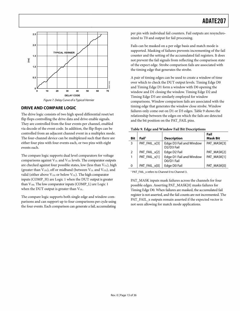
VERNIER RESOLUTION The analog vernier delays are implemented using a modulo 60 algorithm and dividing 2.5 ns into 60 even parts. Because the delays are expressed using a binary representation, an internal mapping algorithm generates the delays. Ignoring analog timing errors, the actual delay produced for the six bits of vernier value (vvvvvv) is expressed as
Delay = (2.5 ns/60) × INT (.5 + (vvvvvv × 60/64))
This mapping results in an inherent discontinuity in the linearity curve.
Figure 7 shows the linearity of a typical vernier. On certain delay codes, the vernier exhibits non-monotonicity. To obtain a monotonic delay curve, these code jumps should be ignored by the user.
ADATE207
Rev. 0 | Page 13 of 36
2.5
2.0
1.5
1.0
0.5
00 7010 20 30 40 50 60
TYPICAL VERNIER
0555
7-01
6
DELAY CODE
(ns)
Figure 7. Delay Curve of a Typical Vernier
DRIVE AND COMPARE LOGIC The drive logic consists of two high speed differential reset/set flip flops controlling the drive data and drive enable signals. They are controlled from the four events per channel, enabled via decode of the event code. In addition, the flip flops can be controlled from an adjacent channel event in a multiplex mode. The four-channel device can be multiplexed such that there are either four pins with four events each, or two pins with eight events each.
The compare logic supports dual level comparators for voltage comparisons against VOL and VOH levels. The comparator outputs are checked against four possible states, low (less than VOL), high (greater than VOH), off or midband (between VOL and VOH), and valid (either above VOH or below VOL). The high comparator inputs (COMP_H) are Logic 1 when the DUT output is greater than VOH. The low comparator inputs (COMP_L) are Logic 1 when the DUT output is greater than VOL.
The compare logic supports both single edge and window com-parisons and can support up to four comparisons per cycle using the four events. Each comparison can generate a fail, accumulating
per pin with individual fail counters. Fail outputs are resynchro-nized to T0 and output for fail processing.
Fails can be masked on a per edge basis and match mode is supported. Masking of failures prevents incrementing of the fail counter and the setting of the accumulated fail registers. It does not prevent the fail signals from reflecting the comparison state of the expect edge. Strobe comparison fails are associated with the timing edge that generates the strobe.
A pair of timing edges can be used to create a window of time over which to check the DUT output levels. Timing Edge D0 and Timing Edge D1 form a window with D0 opening the window and D1 closing the window. Timing Edge D2 and Timing Edge D3 are similarly employed for window comparisons. Window comparison fails are associated with the timing edge that generates the window close strobe. Window failures only come out on D1 or D3 edges. Table 9 shows the relationship between the edges on which the fails are detected and the bit position on the PAT_FAIL pins.
Table 9. Edge and Window Fail Bit Descriptions
Bit Fail1 Description Fail Mask Bit
3 PAT_FAIL_x[3] Edge D3 Fail and Window D2/D3 Fail
PAT_MASK[3]
2 PAT_FAIL_x[2] Edge D2 Fail PAT_MASK[2] 1 PAT_FAIL_x[1] Edge D1 Fail and Window
D0/D1 Fail PAT_MASK[1]
0 PAT_FAIL_x[0] Edge D0 Fail PAT_MASK[0]
1 PAT_FAIL_x refers to Channel 0 to Channel 3.
PAT_MASK inputs mask failures across the channels for four possible edges. Asserting PAT_MASK[0] masks failures for Timing Edge D0. When failures are masked, the accumulated fail register is not asserted, and the fail counts are not incremented. The PAT_FAIL_x outputs remain asserted if the expected vector is not seen allowing for match mode applications.

ADATE207
Rev. 0 | Page 14 of 36
T0 M C
M M
T0 M
INPUT_DELAY
C
4 4 11
C
11PROGRAMMABLERTD DELAY [0:31]
C
1
C
DUT
C
FIFO2
T0
PROGRAMMABLET0 DELAY [0:30]
T0 T0
3
PAT_PATDATA
FAILDUTDATA
LEGEND
1
RTD COMPENSATION
CLK400PIPELINE
REGISTER
MCLKPIPELINE
REGISTER
T0PIPELINEREGISTER
0555
7-00
2
Figure 8. Pipeline Diagram
Dual comparator inputs of the even channels (0 and 2) are routed to the compare logic of adjacent channels to provide ×2 multiplexing. In ×2 multiplexing, Pin 0 and Pin 2 comparator inputs route to Pin 1 and Pin 3, respectively, providing up to eight compare events per cycle on the multiplexed channels.
PIPELINE CONSIDERATIONS For proper functionality, drive actions, compare events, and fail accumulation mask requirements need to be coordinated within the device by adjusting the internal delay paths. The ADATE207 provides two programmable delay paths, the RTD pipeline and the T0 alignment pipeline, as shown in Figure 8. The pattern input and output signals are synchronous with the MCLK and pipelined on T0 periods.
Figure 8 shows the pipeline diagram of the ADATE207. The T0 delay pipeline is programmable. It must be sufficiently deep to cover the round trip delay compensation, yet no deeper than the FIFO depth of the fail logic.
The minimum T0 alignment pipeline depth needed is dependent on the programmed RTD compensation. The programmed T0 alignment pipeline depth must conform to the values listed in Table 10. The maximum number of 30 can be used in any circumstance. Depending upon the MCLK rate and the programmed RTD compensation, a smaller pipeline depth can be used.
Table 10. T0 Pipeline Requirements T0 Alignment Pipelines
Minimum Maximum 10.5 + RTD/4 30
MCLK
QD
CE
T0 PIPELINE
PER_EARLY_T0ENPER_EARLY_C0EN
PAT_PATDATA_x[7:0]PAT_DATA_VALID
PAT_MASK[3:0]INPUT_DELAY[7:0]
0555
7-02
0
Figure 9. PER_EARLY_T0EN Pipelining
Figure 9 shows the pipelining of PER_EARLY_T0EN (the period start signal). It is pipelined with MCLK to control the T0 pipelines within the chip. It uses two MCLK pipelines within the chip to distribute the PER_EARLY_T0EN signal to all of the T0 pipeline registers.
PER_EARLY_T0EN and PER_EARLY_C0EN, the period start signals, and the global INPUT_DELAY signals are pipelined into the ADATE207 with different depths. The PER_EARLY_T0EN and PER_EARLY_C0EN are pipelined with two MCLK pipelines prior to the enable pins of the T0 clocked pipelines. The INPUT_DELAY signals are not pipelined on T0 clock pipelines, but have only two MCLK pipelines prior to use by the timing generators.
Figure 10 shows the relative pipelines for INPUT_DELAY and the period enables.
ADATE207
Rev. 0 | Page 15 of 36
M
PER_EARLY_T0ENPER_EARLY_C0EN
MCLK
INPUT DELAY[7:0]
CE
D Q
T0 PIPELINE
MM
TIMINGGENERATOR
M
0555
7-00
4
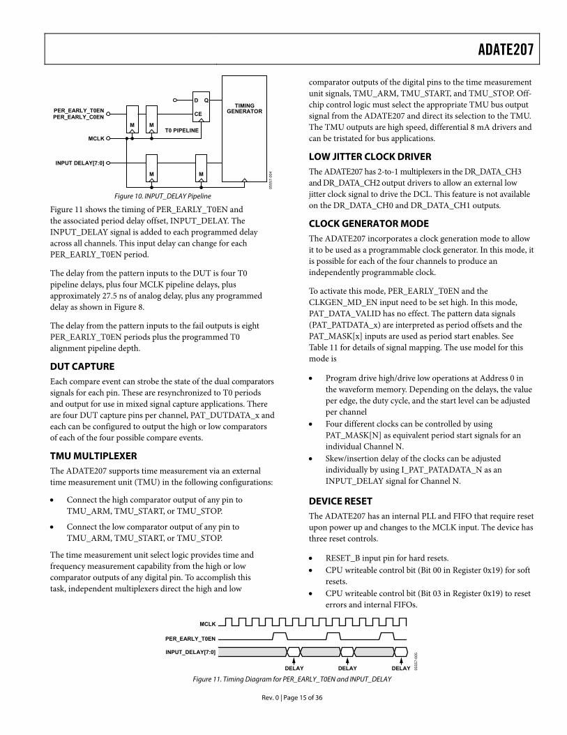
Figure 10. INPUT_DELAY Pipeline
Figure 11 shows the timing of PER_EARLY_T0EN and the associated period delay offset, INPUT_DELAY. The INPUT_DELAY signal is added to each programmed delay across all channels. This input delay can change for each PER_EARLY_T0EN period.
The delay from the pattern inputs to the DUT is four T0 pipeline delays, plus four MCLK pipeline delays, plus approximately 27.5 ns of analog delay, plus any programmed delay as shown in Figure 8.
The delay from the pattern inputs to the fail outputs is eight PER_EARLY_T0EN periods plus the programmed T0 alignment pipeline depth.
DUT CAPTURE Each compare event can strobe the state of the dual comparators signals for each pin. These are resynchronized to T0 periods and output for use in mixed signal capture applications. There are four DUT capture pins per channel, PAT_DUTDATA_x and each can be configured to output the high or low comparators of each of the four possible compare events.
TMU MULTIPLEXER The ADATE207 supports time measurement via an external time measurement unit (TMU) in the following configurations:
• Connect the high comparator output of any pin to TMU_ARM, TMU_START, or TMU_STOP.
• Connect the low comparator output of any pin to TMU_ARM, TMU_START, or TMU_STOP.
The time measurement unit select logic provides time and frequency measurement capability from the high or low comparator outputs of any digital pin. To accomplish this task, independent multiplexers direct the high and low
comparator outputs of the digital pins to the time measurement unit signals, TMU_ARM, TMU_START, and TMU_STOP. Off-chip control logic must select the appropriate TMU bus output signal from the ADATE207 and direct its selection to the TMU. The TMU outputs are high speed, differential 8 mA drivers and can be tristated for bus applications.
LOW JITTER CLOCK DRIVER The ADATE207 has 2-to-1 multiplexers in the DR_DATA_CH3 and DR_DATA_CH2 output drivers to allow an external low jitter clock signal to drive the DCL. This feature is not available on the DR_DATA_CH0 and DR_DATA_CH1 outputs.
CLOCK GENERATOR MODE The ADATE207 incorporates a clock generation mode to allow it to be used as a programmable clock generator. In this mode, it is possible for each of the four channels to produce an independently programmable clock.
To activate this mode, PER_EARLY_T0EN and the CLKGEN_MD_EN input need to be set high. In this mode, PAT_DATA_VALID has no effect. The pattern data signals (PAT_PATDATA_x) are interpreted as period offsets and the PAT_MASK[x] inputs are used as period start enables. See Table 11 for details of signal mapping. The use model for this mode is
• Program drive high/drive low operations at Address 0 in the waveform memory. Depending on the delays, the value per edge, the duty cycle, and the start level can be adjusted per channel
• Four different clocks can be controlled by using PAT_MASK[N] as equivalent period start signals for an individual Channel N.
• Skew/insertion delay of the clocks can be adjusted individually by using I_PAT_PATADATA_N as an INPUT_DELAY signal for Channel N.
DEVICE RESET The ADATE207 has an internal PLL and FIFO that require reset upon power up and changes to the MCLK input. The device has three reset controls.
• RESET_B input pin for hard resets. • CPU writeable control bit (Bit 00 in Register 0x19) for soft
resets. • CPU writeable control bit (Bit 03 in Register 0x19) to reset
errors and internal FIFOs.
MCLK
PER_EARLY_T0EN
INPUT_DELAY[7:0]
DELAY DELAY DELAY 0555
7-00
5
Figure 11. Timing Diagram for PER_EARLY_T0EN and INPUT_DELAY
ADATE207
Rev. 0 | Page 16 of 36
After the power and MCLK inputs are stable, the device must be reset using the hard reset and error reset bits. The soft reset can be used to initialize registers at any time and does not reset the PLL or FIFOs.
There are six rules of reset.
Rule 1—on power up, keep the hard reset pin (RESET_B) asserted.
Rule 2—if MCLK is unstable, keep the hard reset pin (RESET_B) asserted.
Rule 3—after MCLK is stable, keep the hard reset pin (RESET_B) asserted for at least 20 μs.
Rule 4—after the 20 μs of Rule 3 has elapsed, assert the error reset bit (Bit 03 in Register 0x19).
Rule 5—the hard reset signal (RESET_B) can be asserted asynchronously to MCLK, but upon deassertion, must make setup and hold requirements upon the MCLK.
Rule 6—the minimum pulse width of RESET_B must be at least three MCLK periods.
Table 11. Comparison Between Normal Mode and Clock Generation Mode Normal Mode (CLKGEN_MD_EN=0) Clock Generator Mode(CLKGEN_MD_EN=1) Period Start A single signal for all four channels, I_PER_EARLY_T0EN. Four signals, one per channel; PAT_MASK[N] operates
as a period start signal for channel N. Waveform Memory Selection
Each channel N is selected via the I_PAT_PATDATA_N vector every rising edge of I_MCLK.
Waveform memory location is fixed at Address 0.
Input Delay A single vector adjust input delay for all channels, INPUT_DELAY.
Four vectors are available, one per channel. For each Channel N, PAT_PATDATA_N operates as INPUT_DELAY for Channel N.
Fail Masking Edge N for all channels can mask the fail operation every rising edge of I_MCLK via PAT_MASK[N].
No masking of fail operations is available.
ADATE207
Rev. 0 | Page 17 of 36
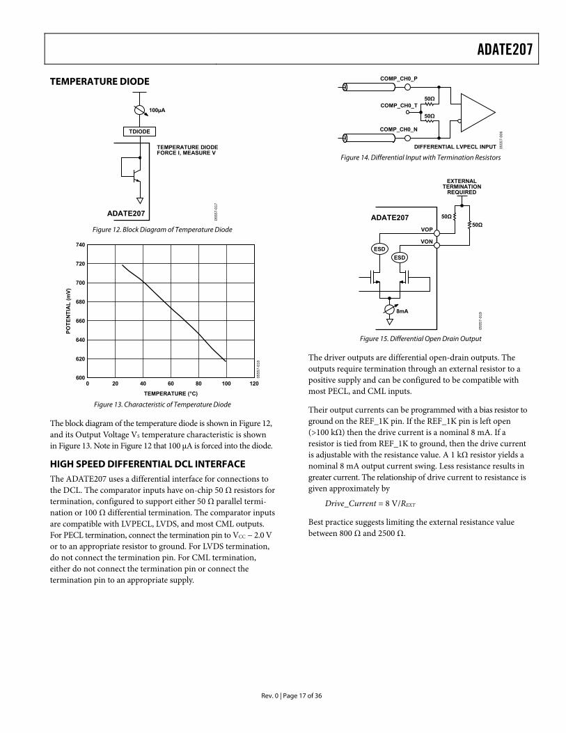
TEMPERATURE DIODE
ADATE207
100µA
TDIODE
TEMPERATURE DIODEFORCE I, MEASURE V
0555
7-01
7
Figure 12. Block Diagram of Temperature Diode
740
6000
TEMPERATURE (°C)
POTE
NTI
AL
(mV)
120
720
700
680
660
640
620
20 40 60 80 100
0555
7-01
8
Figure 13. Characteristic of Temperature Diode
The block diagram of the temperature diode is shown in Figure 12, and its Output Voltage VS temperature characteristic is shown in Figure 13. Note in Figure 12 that 100 μA is forced into the diode.
HIGH SPEED DIFFERENTIAL DCL INTERFACE The ADATE207 uses a differential interface for connections to the DCL. The comparator inputs have on-chip 50 Ω resistors for termination, configured to support either 50 Ω parallel termi-nation or 100 Ω differential termination. The comparator inputs are compatible with LVPECL, LVDS, and most CML outputs. For PECL termination, connect the termination pin to VCC − 2.0 V or to an appropriate resistor to ground. For LVDS termination, do not connect the termination pin. For CML termination, either do not connect the termination pin or connect the termination pin to an appropriate supply.
50Ω
COMP_CH0_P
COMP_CH0_T
COMP_CH0_N
50Ω
DIFFERENTIAL LVPECL INPUT 0555
7-00
6
Figure 14. Differential Input with Termination Resistors
8mA
ADATE207VOP
VON
50Ω50Ω
EXTERNALTERMINATION
REQUIRED
ESDESD
0555
7-01
9
Figure 15. Differential Open Drain Output
The driver outputs are differential open-drain outputs. The outputs require termination through an external resistor to a positive supply and can be configured to be compatible with most PECL, and CML inputs.
Their output currents can be programmed with a bias resistor to ground on the REF_1K pin. If the REF_1K pin is left open (>100 kΩ) then the drive current is a nominal 8 mA. If a resistor is tied from REF_1K to ground, then the drive current is adjustable with the resistance value. A 1 kΩ resistor yields a nominal 8 mA output current swing. Less resistance results in greater current. The relationship of drive current to resistance is given approximately by
Drive_Current = 8 V/REXT
Best practice suggests limiting the external resistance value between 800 Ω and 2500 Ω.
ADATE207
Rev. 0 | Page 18 of 36
CONTROL AND STATUS REGISTER INTERFACE The ADATE207 uses a general-purpose, 16-bit bidirectional, multiplexed address data bus for computer access of the control and status registers of the part. All bus activity is registered at the interface synchronous to the master clock (MCLK), which is also used by the part for delay timing. Operations the bus supports include random access reads and writes, as well as the ability to access blocks of registers in burst.
A description of each register is contained in the Control and Status Registers section of this document.
READ/WRITE FUNCTION The control and status register (CSR) bus interface supports the following functionalities:
• The ability to enable groups of channels for write operations, allowing simultaneous programming across all the designated channels.
• The ability to select any single channel, or group of channels, to poll (read) status (where the return value is the bitwise logical OR of the status returned from each of the designated channels).
• The ability to read or write in a single burst operation to a sequential block of registers significantly reducing the time required to program the internal memories.
In multiplexing the address and data on the bus, each operation takes at least two cycles to complete. In all cases, read or write, the first cycle provides the 16-bit address. This cycle is followed
by one or more data cycles. The quantity of data cycles is dependent on the activity on the CS_AD and CS_RW_B lines, which determine the type of operation to perform.
The 16-bit address provided in the first cycle is comprised of two 5-bit address fields and an additional control field of 6-bits as shown in Table 12. The control field extends the associated 5-bit register address in use by steering the address and data to one or more banks of registers within the part.
Register address space consists of five identifiable banks or groups of register implementations. These include one set of registers for each of the four channels and a fifth or common register space. Five bits of addressing are available to all five address spaces. The bank of registers for each channel duplicates the other in function and address, allowing a single write operation to be steered to multiple channels for simultaneous programming. The fifth bank of registers provides shared functions, common to all four channels, whose address range is mapped outside of the register address space used by the individual channel functions.
All single register, random access operations are performed with the burst bit of the control field disabled. For these types of transactions, the 5-bit stop address field is ignored, and the 5-bit start address field is used as the register address of the operation.
Table 12. Address Bus Decoding Address Bits Description Bit 15 Burst Enable. 1 = initiate burst mode operation. 0 = enable normal read or write transactions. Bit 14 Common Enable. When set to 1, enables reads or writes to the common registers. This enable is valid in
either normal or burst modes. Bit 13 Channel 3 Enable. When set to 1, enables reads or writes to Channel 3. This enable is valid in either
normal or burst modes. Bit 12 Channel 2 Enable. When set to 1, enables reads or writes to Channel 2. This enable is valid in either
normal or burst modes. Bit 11 Channel 1 Enable. When set to 1, enables reads or writes to Channel 1. This enable is valid in either
normal or burst modes. Bit 10 Channel 0 Enable. When set to 1, enables reads or writes to Channel 0. This enable is valid in either
normal or burst modes. Bits[09:05] Burst Stop Address. Used to set the last CSR address to read to, or write from, before looping back to the
burst start address. This address is only valid when burst enable is set to 1. Bits[04: 00] CSR Address (Burst Enable = 0). Used to set the CSR address for reading or writing.
Burst Start Address (Burst Enable = 1). Used to set the first CSR address to read to, or write from, when bursting data. Burst writes or reads incrementally access successive registers up to, and including, the burst stop address.

ADATE207
Rev. 0 | Page 19 of 36
MCLKCYCLES
RD3 A4 WD4
CS_AS
CS_RW_B
CS_AD A1 WD1 A2 WD2 A3
1 CYCLE OF BUS TURN-AROUND + 8 CYCLES OF READ DATA DELAY 1 CYCLE OF BUS TURN-AROUND
ASSERTED FOR 2 OR MORE CYCLES WILL ALLOW1 EXTRA CYCLE OF READ DATA HOLD ON BUS
(OPTIONAL)
0555
7-01
0
Figure 16. Bus Interface Function Timing Diagram
Figure 16 shows the bus functional timing while performing both read and write operations. Highlights include
• The bus implements a synchronous protocol, where read and write transactions are slotted into MCLK cycles.
• The CS_AD bus lines, 2.5 V CMOS signals, can be tri-stated. To implement a multidrop bus, strict adherence to proper bus turnaround from reads to writes (and vice versa) is required.
• The initial bus turn around time for a read operation is indicative of the internal path length inside the ADATE207.
• After accepting a read transaction, the ADATE207 waits one MCLK cycle for bus turnaround, and then turns on its bus drivers to precharge the bus.
• There must be at least one MCLK cycle between a read followed by a write transaction, and between the address and read data cycles due to bus turnaround. The ADATE207 tristates the bus on the MCLK after it has finished driving the read data.
• A write transaction can be followed immediately by a read transaction. Likewise, a series of write transactions can be grouped together with no dead time in between transactions.
• To ease board timing, holding the CS_RW_B signal high allows the read data to stay on the bus one extra MCLK cycle. One application allows two clock cycles for read data to propagate to its destination. Note that holding CS_RW_B high for more that two cycles has no effect.
All external bus signals come into the ADATE207 and are registered by the MCLK. Then, the registered signals are used to interface to the four channel-specific register banks and the common block. Each register bank receives an address, data, the read/write signal, and a block select. Even though some portions of the internal timing circuitry run at a high rate than the master clock, all of the register blocks run at the master clock, MCLK, rate.
When a block is selected, a read or write operation is performed. For read operations, data is enabled onto the read data bus of a block, and that data is OR’ed with four other block-specific RDATA busses to form the read data that is sent from the
ADATE207. Note that the read data takes more than one clock cycle. The bus interface state machine controls the output enable accordingly.
The write data is reregistered (retimed) to require only one MCLK cycle to write the data into the targeted register (or registers, in the case where multiple channels are selected).
Burst Mode
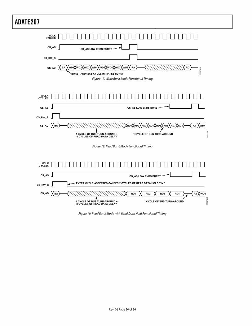
Burst mode is a special mode that allows for successive reads or writes with a predetermined addressing scheme. Figure 17 shows the burst mode operation of the bus. The primary purpose of burst mode is to allow fast writes into the waveform memory for each channel. Burst mode is initiated and completely controlled via the bus interface pins of the ADATE207.
Burst mode is initiated with a special address cycle, as defined in Table 12. Burst mode cycles are shown in Figure 17 through Figure 19 and incorporate the following conditions:
• The completion of burst mode is controlled by the address strobe signal. If address strobe is deasserted in a particular MCLK cycle, that becomes the last cycle of the burst.
• Only a series of burst writes or reads can occur. There can be no mixing of reads and writes in a burst sequence.
• The bus interface state machine takes over the internal register address only and the read/write selection signal.
• The CSR blocks and channel-specific memory accesses operate the same in burst mode as they do in the normal read/write transactions.
• There must be at least two MCLK cycles between a read burst followed by another read or write transaction, and between the address and read data cycles due to bus turn-around. The ADATE207 tristates the bus on the MCLK after it is finished driving read data, as shown in Figure 18.
• When extended read data hold mode is selected during a read burst, the internal address bus increments every other cycle, causing read data on the CS_AD bus to change every other cycle, as shown in Figure 19.
ADATE207
Rev. 0 | Page 20 of 36
MCLKCYCLES
RD
CS_AS LOW ENDS BURST
BURST ADDRESS CYCLE INITIATES BURST
CS_AS
CS_RW_B
CS_AD RABA WD1 WD3WD2 WD4 WD5 WD7WD6 WD8
0555
7-01
1
Figure 17. Write Burst Mode Functional Timing
BA
1 CYCLE OF BUS TURN-AROUND1 CYCLE OF BUS TURN-AROUND +8 CYCLES OF READ DATA DELAY
MCLKCYCLES
CS_AS
CS_RW_B
CS_AD
CS_AS LOW ENDS BURST
WD4RD1 RD3RD2 RD4 RD5 RD7RD6 RD8 A4
0555
7-01
2
Figure 18. Read Burst Mode Functional Timing
BA WD4RD1 RD2 RD3 RD4 A4
1 CYCLE OF BUS TURN-AROUND1 CYCLE OF BUS TURN-AROUND +8 CYCLES OF READ DATA DELAY
MCLKCYCLES
CS_AS
CS_RW_B
CS_AD
EXTRA CYCLE ASSERTED CAUSES 2 CYCLES OF READ DATA HOLD TIME
CS_AS LOW ENDS BURST
0555
7-01
3
Figure 19. Read Burst Mode with Read Data Hold Functional Timing
ADATE207
Rev. 0 | Page 21 of 36
CONTROL AND STATUS REGISTERS This section details the breakdown of the configuration and status registers in the ADATE207. An address map provides the locations of all registers, and the detailed descriptions that follow show how each register is used.
Table 13. Address Map Chip Address Register Description 0x00 Comparator and Fail Status. Channel-specific address space. 0x01 Fail Counter Low. 0x02 Fail Counter High. 0x03 Static Configuration. 0x04 Dynamic Configuration. 0x05 Waveform/Calibration Memory Address. 0x06 Waveform D0 Vernier Delay and Action. 0x07 Waveform D0 Course Delay. 0x08 Waveform D1 Vernier Delay and Action. 0x09 Waveform D1 Course Delay. 0x0A Waveform D2 Vernier Delay and Action. 0x0B Waveform D2 Course Delay. 0x0C Waveform D3 Vernier Delay and Action. 0x0D Waveform D3 Course Delay. 0x0E Calibration Memory D0. 0x0F Calibration Memory D1. 0x10 Calibration Memory D2. 0x11 Calibration Memory D3. 0x12 DUT Data Selection. 0x13 to 0x18 Unused. Reserved. 0x19 Software Resets. Common register address space. 1x1A Round Trip Delay Value. 0x1B T0 Alignment Pipeline Depth. 0x1C TMU Channel Select. 0x1D Channel Multiplex Enable. 0x1E Channel Status. 0x1F Chip Information.
ADATE207
Rev. 0 | Page 22 of 36
CHANNEL SPECIFIC AND COMMON REGISTERS Detailed register descriptions divided into channel-specific and common registers.
Channel Specific Registers
Name: Comparator and Fail Status
Address: 0x00
Type: Read
Table 14. Comparator and Fail Status Position Description Reset State Bits[15:08] Not used. 0x00 Bit 07 Edge Error: Edges Longer Than 4 T0 Cycles. This occurs when the edge delay counters are reloaded
before they complete counting down, thus, causing a missing edge. 0x0
Bit 06 Edge Error: Out of Order Edge Strobes. This occurs when one or more edge delay counters complete counting out of order (wrong action code is paired with an edge), or two edge delay counters complete counting at the same CLK400 edge (causing a missing edge).
0x0
Bit 05 Edge Error: Adder Overflow. This occurs when the residue or calibration constant adders overflow causing edge delays to wrap around. This results in incorrect edge timing.
0x0
Bit 04 Edge Error: Two Edges Too Close. This occurs when either the drive or compare verniers receive nonincreasing delay values in back-to-back CLK400 cycles. The verniers become unsynchronized and cause incorrect edge timing thereafter.
0x0
Bits[03:00] Accumulated Fail Registers. These four data bits provide up to four possible DUT failures—one for each edge delay. The bits are decoded as follows:
0x0
Bit 00 = D0 edge or window failures. Bit 01 = D1 edge failure or D0/D1 window failures. Bit 02 = D2 edge or window failures. Bit 03 = D3 edge failure or a D3/D2 window failure.
Name: Fail Counter Low
Address: 0x01
Type: Read/Write
Table 15. Fail Counter Low Position Description Reset State Bits[15:00] Fail Counter Data Low Order Bits. This field contains the 16 LSBs of the fail counter. This register and the
fail counter data high register represent a binary encoded, 32-bit, number of fail events (up to 4 fail events per T0 period) detected during the last pattern burst. The CPU reads this register while the pattern is bursting, capturing a snapshot of the fail count at the time of reading the low register. Writes during pattern burst can produce indeterminate results if fails are occurring during the write cycle. The CPU must read the contents of the counter by performing sequential reads from the fail counter low register followed by a read from the fail counter high register. Reading from the fail counter low register performs the transfer of data from the counter to a temporary holding register. Reading from the fail counter high register reads solely from the temporary holding register. For diagnostics, the CPU can preload the contents of the counter by performing sequential writes to the Fail Counter CHx data low register followed by a write to the Fail Counter Chx data high register. Writing to the Fail Counter Chx data high register performs the transfer of data from temporary holding registers to the 32-bit counter.
0x0000
ADATE207
Rev. 0 | Page 23 of 36
Name: Fail Counter High
Address: 0x02
Type: Read/Write
Table 16. Fail Counter High Position Description Reset State Bits[15:00] Fail Counter Data High. This field contains the 16 MSBs of the fail counter. See Table 15, the fail
counter low register, for more information. 0x0000
Name: Static Configuration
Address: 0x03
Type: Read/Write
Table 17. Static Configuration Position Description Reset State Bits[15:04] Not Used. 0x000 Bit 03 Ch_Data_Low. 0
A high with edges disabled produces a low level output from the drive data (DR_DATA) signal regardless of pattern data.
Pulsing this bit allows the data to be preset to a low level output prior to bursting a pattern. Control of the drive data is pattern data dependent when a pattern is burst. If both Data_High and Data_Low are high, the data is indeterminate.
Bit 02 Ch_Data_High. 0 A high with edges disabled produces a high level output from the drive data (DR_DATA) signal
regardless of pattern data
Pulsing this bit allows the data to be preset to a high level output prior to bursting a pattern. Control of the drive data is pattern data dependent when a pattern is burst.
Bit 01 Ch_Driver_Off. 0 A high with edges disabled produces a low level output from the drive enable (DR_EN) signal,
tristating the driver regardless of pattern data.
Pulsing this bit allows the driver to tristate prior to bursting a pattern. Control of the driver is pattern data dependent when a pattern is burst. If both Driver_On and Driver_Off are high, the drive enable signal (DR_EN) is indeterminate.
Bit 00 Ch_Driver_On. 0 A high with edges disabled produces high level output from the drive enable (DR_EN) signal,
enabling the driver regardless of pattern data.
Pulsing this bit enables the driver prior to bursting a pattern. Control of the driver is pattern data dependent when a pattern is burst.
ADATE207
Rev. 0 | Page 24 of 36
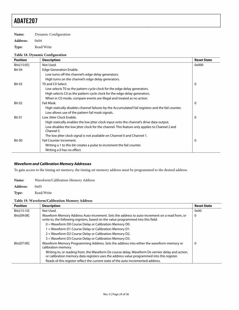
Name: Dynamic Configuration
Address: 0x04
Type: Read/Write
Table 18. Dynamic Configuration Position Description Reset State Bits[15:05] Not Used. 0x000 Bit 04 Edge Generation Enable.
Low turns off the channel’s edge delay generators. High turns on the channel’s edge delay generators.
Bit 03 T0 and C0 Select. 0 Low selects T0 as the pattern cycle clock for the edge delay generators. High selects C0 as the pattern cycle clock for the edge delay generators. When in C0 mode, compare events are illegal and treated as no action.
Bit 02 Fail Mask. 0 High statically disables channel failures by the Accumulated Fail registers and the fail counter. Low allows use of the pattern fail mask signals.
Bit 01 Low Jitter Clock Enable. 0 High statically enables the low jitter clock input onto the channel’s drive data output. Low disables the low jitter clock for the channel. This feature only applies to Channel 2 and
Channel 3.
The low jitter clock signal is not available on Channel 0 and Channel 1. Bit 00 Fail Counter Increment. 0
Writing a 1 to this bit creates a pulse to increment the fail counter. Writing a 0 has no effect.
Waveform and Calibration Memory Addresses
To gain access to the timing set memory, the timing set memory address must be programmed to the desired address.
Name: Waveform/Calibration Memory Address
Address: 0x05
Type: Read/Write
Table 19. Waveform/Calibration Memory Address Position Description Reset State Bits[15:10] Not Used. 0x00 Bits[09:08] Waveform Memory Address Auto-Increment. Sets the address to auto-increment on a read from, or
write to, the following registers, based on the value programmed into this field: 0
0 = Waveform D0 Course Delay or Calibration Memory D0. 1 = Waveform D1 Course Delay or Calibration Memory D1. 2 = Waveform D2 Course Delay or Calibration Memory D2. 3 = Waveform D3 Course Delay or Calibration Memory D3.
Bits[07:00] Waveform Memory Programming Address. Sets the address into either the waveform memory or calibration memory.
0
Writing to, or reading from, the Waveform Dx course delay, Waveform Dx vernier delay and action, or calibration memory data registers uses the address value programmed into this register.
Reads of this register reflect the current state of the auto-incremented address.

ADATE207
Rev. 0 | Page 25 of 36
Name: Waveform D0 Vernier Delay and Action
Address: 0x06
Type: Read/Write
Table 20. Waveform D0 Vernier Delay and Action Position Description Reset State Bits[15:10] D0 Vernier Delay. The vernier delay is represented in binary by the equation, vvvvvv × (2.5 ns/64). Undefined Bits[09:04] Not Used. 0x00 Bits[03:00] D0 Action. A binary encoded data field. Undefined 0x0 = no action. 0x1 = drive low. 0x2 = drive high. 0x3 = force off. 0x4 = force on. 0x5 = force down. 0x6 = force up. 0x7 = edge compare low. 0x8 = edge compare high. 0x9 = edge compare off. 0xA = edge compare valid. 0xB = open window low. 0xC = open window high. 0xD = open window high-Z. 0xE = open window valid. 0xF = compare unknown.
Name: Waveform D0 Vernier Delay and Action
Address: 0x07
Type: Read/Write
Table 21. Waveform D0 Course Delay Position Description Reset State Bits[15:00] D0 Course Delay. Number of 2.5 ns clock periods to count. When this count is completed, the vernier
delay (defined by the D0 vernier value programmed into the Waveform D0 vernier delay and action register) is added to the D0 course delay to place an edge in time. Waveform D0 vernier delay and action must be written immediately before this register for the waveform memory to be written correctly.
Undefined

ADATE207
Rev. 0 | Page 26 of 36
Name: Waveform D1 Vernier Delay and Action
Address: 0x08
Type: Read/Write
Table 22. Waveform D1 Vernier Delay and Action Position Description Reset State Bits[15:10] D1 Vernier Delay. The vernier delay is represented in binary by the equation, vvvvvv × (2.5 ns/64). Undefined Bits[09:04] Not Used. 0x00 Bits[03:00] D1 Action. A binary encoded data field. Undefined 0x0 = no action. 0x1 = drive low. 0x2 = drive high. 0x3 = force off. 0x4 = force on. 0x5 = force down. 0x6 = force up. 0x7 = edge compare low. 0x8 = edge compare high. 0x9 = edge compare off.
0xA = edge compare valid. 0xF = close window/compare unknown.
Name: Waveform D1Course Delay
Address: 0x09
Type: Read/Write
Table 23. Waveform D1 Course Delay Position Description Reset State Bits[15:00] D1 Course Delay. Number of 2.5 ns clock periods to count. Undefined
When this count is completed, add the vernier delay (defined by the D1 vernier value programmed into the waveform D1 vernier delay and action register) to the D1 course delay to place an edge in time.
Waveform D1 vernier delay and action must be written immediately before this register for the waveform memory to be correctly written.

ADATE207
Rev. 0 | Page 27 of 36
Name: Waveform D2 Vernier Delay and Action
Address: 0x0A
Type: Read/Write
Table 24. Waveform D2 Vernier Delay and Action Position Description Reset State Bits[15:10] D2 Vernier Delay: The vernier delay is represented in binary by the equation,
vvvvvv × (2.5 ns/64) Undefined
Bits[09:04] Not Used. 0x00 Bits[03:00] D2 Action. A binary encoded data field. Undefined 0x0 = no action. 0x1 = drive low. 0x2 = drive high. 0x3 = force off. 0x4 = force on. 0x5 = force down. 0x6 = force up.
0x7 = edge compare low. 0x8 = edge compare high. 0x9 = edge compare off. 0xA = edge compare valid. 0xB = open window low. 0xC = open window high. 0xD = open window high-Z. 0xE = open window valid. 0xF = compare unknown.
Name: Waveform D2 Course Delay
Address: 0x0B
Type: Read/Write
Table 25. Waveform D2 Course Delay Position Description Reset State Bits[15:00] D2 Course Delay. Number of 2.5 ns clock periods to count. Undefined When this count is completed, the vernier delay (defined by the D2 vernier value programmed
into the waveform D2 vernier delay and action register) is added to the D2 course delay to place an edge in time
Waveform D2 vernier delay and action must be written immediately before this register for the waveform memory to be correctly written.

ADATE207
Rev. 0 | Page 28 of 36
Name: Waveform D3 Vernier Delay and Action
Address: 0x0C
Type: Read/Write
Table 26. Waveform D3 Vernier Delay and Action Position Description Reset State Bits[5:10] D3 Vernier Delay: The vernier delay is represented in binary by the equation, vvvvvv × (2.5 ns/64) Undefined Bits[09:04] Not Used. D3 Action: A binary encoded data field. 0x0 = no action. 0x1 = drive low. 0x2 = drive high. 0x3 = force off. Bits[03:00] 0x4 = force on. Undefined 0x5 = force down. 0x6 = force up. 0x7 = edge compare low. 0x8 = edge compare high. 0x9 = edge compare off. 0xA = edge compare valid. 0xF = close window/compare unknown.
Name: Waveform D3 Course Delay
Address: 0x0D
Type: Read/Write
Table 27. Waveform D3 Course Delay Position Description Reset State Bits[15:00] D3 Course Delay. Number of 2.5 ns clock periods to count. Undefined
When this count is completed, the vernier delay (defined by the D3 vernier value programmed into the waveform D3 vernier delay and action register) is added to the D3 course delay to place an edge in time.
Waveform D3 vernier delay and action must be written immediately before this register for the waveform memory to be correctly written.
Name: Calibration Memory D0
Address: 0x0E
Type: Read/Write
Table 28. Calibration Memory D0 Position Description Reset State Bits[15:08] Not Used. 0x000 Bits[07:00] D0 Calibration Constant (CCCCCCCC). The calibration delay is represented in binary by the equation
CCCCCCCC × (2.5 ns/64). Undefined
ADATE207
Rev. 0 | Page 29 of 36
Name: Calibration Memory D1
Address: 0x0F
Type: Read/Write
Table 29. Calibration Memory D1 Position Description Reset State Bits[15:08] Not Used. 0x000 Bits[07:00] D1 Calibration Constant (CCCCCCCC). The calibration delay is represented in binary by the equation
CCCCCCCC × (2.5 ns/64) Undefined
Name: Calibration Memory D2
Address: 0x10
Type: Read/Write
Table 30. Calibration Memory D2 Position Description Reset State Bits[15:08] Not Used. 0x000 Bits[07:00] D2 Calibration Constant (CCCCCCCC). The calibration delay is represented in binary by the equation
CCCCCCCC × (2.5 ns/64) Undefined
Name: Calibration Memory D2
Address: 0x11
Type: Read/Write
Table 31. Calibration Memory D3 Position Description Reset State Bits[15:08] Not Used. 0x000 Bits[07:00] D3 Calibration Constant (CCCCCCCC). The calibration delay is represented in binary by the equation
CCCCCCCC × (2.5 ns/64). Undefined
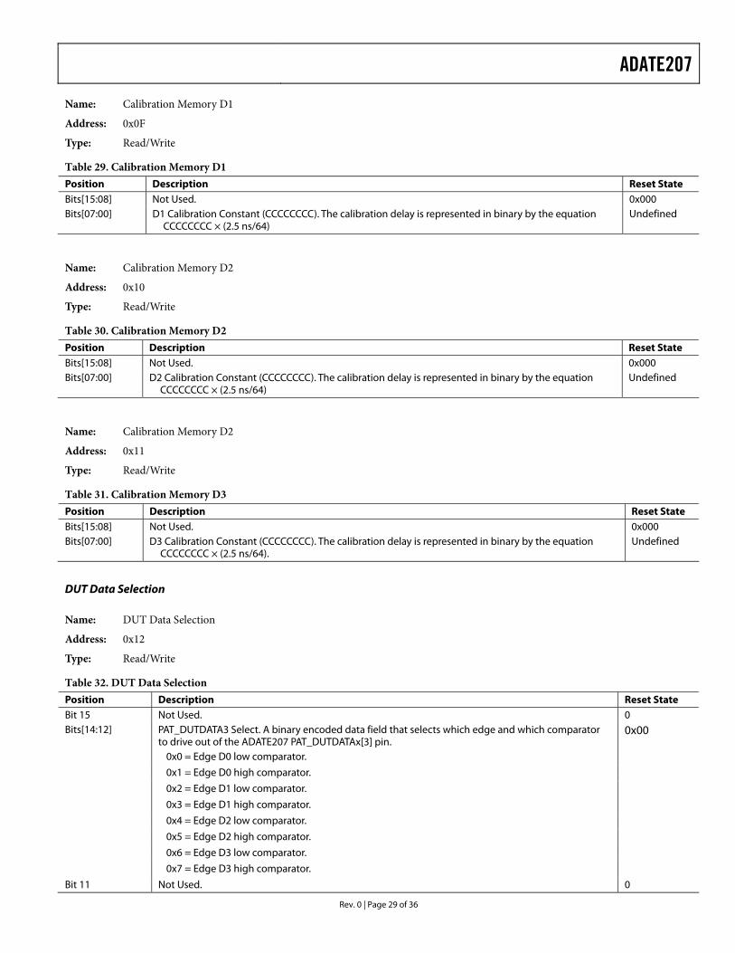
DUT Data Selection
Name: DUT Data Selection
Address: 0x12
Type: Read/Write
Table 32. DUT Data Selection Position Description Reset State Bit 15 Not Used. 0 Bits[14:12] PAT_DUTDATA3 Select. A binary encoded data field that selects which edge and which comparator
to drive out of the ADATE207 PAT_DUTDATAx[3] pin. 0x00
0x0 = Edge D0 low comparator. 0x1 = Edge D0 high comparator. 0x2 = Edge D1 low comparator. 0x3 = Edge D1 high comparator. 0x4 = Edge D2 low comparator. 0x5 = Edge D2 high comparator. 0x6 = Edge D3 low comparator. 0x7 = Edge D3 high comparator. Bit 11 Not Used. 0
ADATE207
Rev. 0 | Page 30 of 36
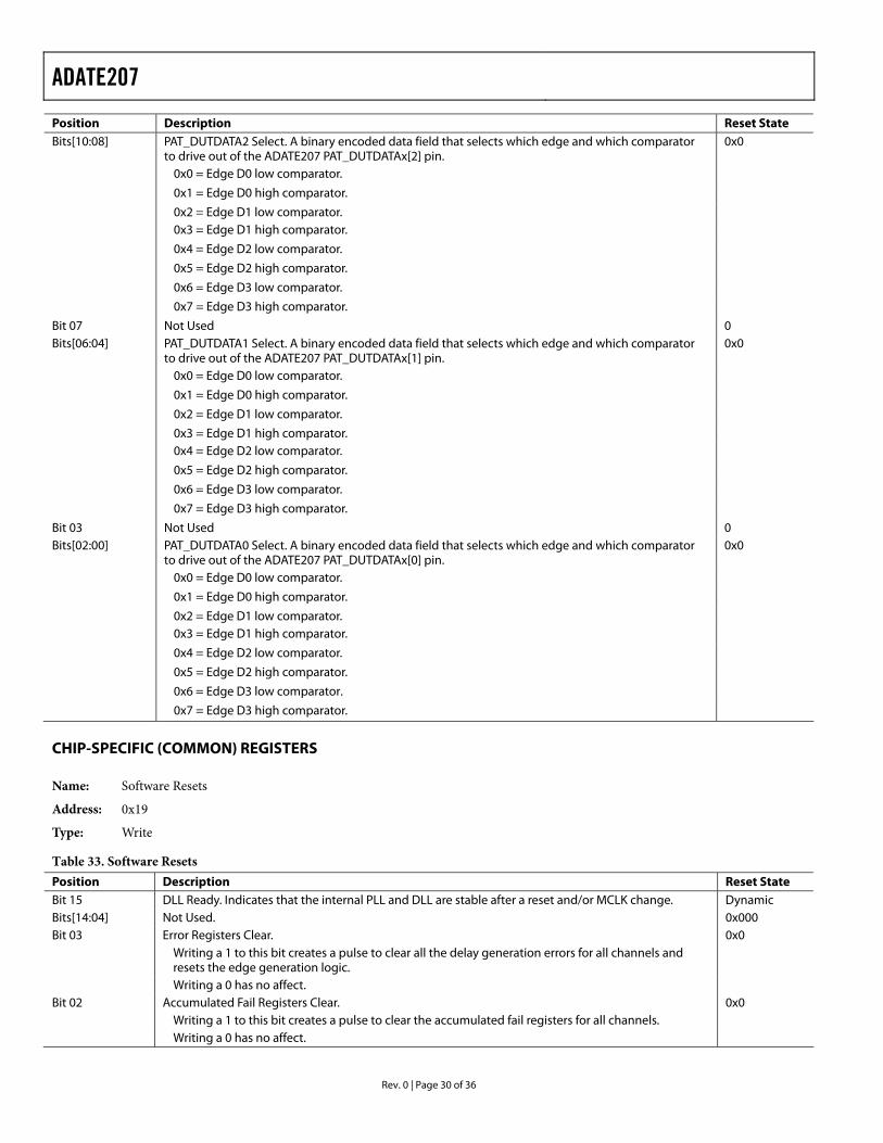
Position Description Reset State Bits[10:08] PAT_DUTDATA2 Select. A binary encoded data field that selects which edge and which comparator
to drive out of the ADATE207 PAT_DUTDATAx[2] pin. 0x0
0x0 = Edge D0 low comparator. 0x1 = Edge D0 high comparator. 0x2 = Edge D1 low comparator. 0x3 = Edge D1 high comparator. 0x4 = Edge D2 low comparator. 0x5 = Edge D2 high comparator. 0x6 = Edge D3 low comparator. 0x7 = Edge D3 high comparator. Bit 07 Not Used 0 Bits[06:04] PAT_DUTDATA1 Select. A binary encoded data field that selects which edge and which comparator
to drive out of the ADATE207 PAT_DUTDATAx[1] pin. 0x0
0x0 = Edge D0 low comparator. 0x1 = Edge D0 high comparator. 0x2 = Edge D1 low comparator. 0x3 = Edge D1 high comparator. 0x4 = Edge D2 low comparator. 0x5 = Edge D2 high comparator. 0x6 = Edge D3 low comparator. 0x7 = Edge D3 high comparator. Bit 03 Not Used 0 Bits[02:00] PAT_DUTDATA0 Select. A binary encoded data field that selects which edge and which comparator
to drive out of the ADATE207 PAT_DUTDATAx[0] pin. 0x0
0x0 = Edge D0 low comparator. 0x1 = Edge D0 high comparator. 0x2 = Edge D1 low comparator. 0x3 = Edge D1 high comparator. 0x4 = Edge D2 low comparator. 0x5 = Edge D2 high comparator. 0x6 = Edge D3 low comparator. 0x7 = Edge D3 high comparator.
CHIP-SPECIFIC (COMMON) REGISTERS
Name: Software Resets
Address: 0x19
Type: Write
Table 33. Software Resets Position Description Reset State Bit 15 DLL Ready. Indicates that the internal PLL and DLL are stable after a reset and/or MCLK change. Dynamic Bits[14:04] Not Used. 0x000 Bit 03 Error Registers Clear. 0x0 Writing a 1 to this bit creates a pulse to clear all the delay generation errors for all channels and
resets the edge generation logic.
Writing a 0 has no affect. Bit 02 Accumulated Fail Registers Clear. 0x0 Writing a 1 to this bit creates a pulse to clear the accumulated fail registers for all channels. Writing a 0 has no affect.

ADATE207
Rev. 0 | Page 31 of 36
Position Description Reset State Bit 01 Fail Counters Clear. 0x0 Writing a 1 to this bit creates a pulse to clear the fail counters for all channels. Writing a 0 has no affect. Bit 00 Soft Reset. Writing this register bit to a Logic 1 causes the ADATE207 to generate a software reset. This
is logically equivalent to a hard reset via the I_RESET_B pin. All logic and registers are reset.
0x0
Name: Round Trip Delay Value
Address: 0x1A
Type: Read/Write
Table 34. Round Trip Delay Value Position Description Reset State Bits[15:05] Not Used. 0x000 Bits[4:00] Round Trip Delay Value. Programs the round-trip delay from the ADATE207 drive to compare pins, in
units of 2.5 ns. The maximum delay is 80 ns (value = 31) and the minimum delay is 2.5 ns (value = 0). 0x0
Name: T0 Alignment Pipeline Depth
Address: 0x1B
Type: Read/Write
Table 35. T0 Alignment Pipeline Depth Position Description Reset State Bits[15:05] Not Used. 0x000 Bits[04:00] T0 Alignment Pipeline Depth. This pipeline value matches the edge generation delay for compare
edges thereby correctly aligning compare fails and DUT data to the T0 pipeline. It should be programmed no higher than 30 and ≥ 10.5+ RTD/4.
0x0
TMU Channel Select This register selects one of four channels to independently direct to the TMU arm, start, and stop buses.
Name: TMU Channel Select
Address: 0x1C
Type: Read/Write
Table 36. TMU Channel Select Position Description Reset State Bits[15:12] Not Used. 0x00 Bit 11 TMU Stop Enable. A zero tristates the TMU stop output. 0 Bits[10:08] TMU Stop, Channel Select Multiplexer. A binary encoded data field. 0x00 0x0 selects Channel 0 comparator high. 0x1 selects Channel 0 comparator low. 0x2 selects Channel 1 comparator high. 0x3 selects Channel 1 comparator low. 0x4 selects Channel 2 comparator high. 0x5 selects Channel 2 comparator low. 0x6 selects Channel 3 comparator high. 0x7 selects Channel 3 comparator low. Bit 07 TMU Start Enable. A zero tristates the TMU stop output. 0 Bits[06:04] TMU Start, Channel Select Multiplexer. A binary encoded data field. 0x00

ADATE207
Rev. 0 | Page 32 of 36
Position Description Reset State 0x0 selects Channel 0 comparator high. 0x1 selects Channel 0 comparator low. 0x2 selects Channel 1 comparator high. 0x3 selects Channel 1 comparator low. 0x4 selects Channel 2 comparator high. 0x5 selects Channel 2 comparator low. 0x6 selects Channel 3 comparator high. 0x7 selects Channel 3 comparator low. Bit 03 TMU Arm Enable. A zero tristates the TMU Stop output. 0 Bits[02:00] TMU Arm Channel Select Multiplexer. A binary encoded data field. 0x00 0x0 selects Channel 0 comparator high. 0x1 selects Channel 0 comparator low. 0x2 selects Channel 1 comparator high. 0x3 selects Channel 1 comparator low. 0x4 selects Channel 2 comparator high. 0x5 selects Channel 2 comparator low. 0x6 selects Channel 3 comparator high. 0x7 selects Channel 3 comparator low.
Name: Channel Multiplex Enable
Address: 0x1D
Type: Read/Write
Table 37. Channel Multiplex Enable Position Description Reset State Bits[15:02] Not Used. 0x0000 Bit 01 CH2 Multiplex Enable. This channel can be 2-way multiplexed. Setting this bit to 1 enables Channel 3
to be multiplexed on Channel 2. 0
Bit 00 CH0 Multiplex Enable. This channel can be 2-way multiplexed. Setting this bit to 1 enables Channel 1 to be multiplexed on Channel 0.
0
Name: Channel Status
Address: 0x1E
Type: Read
Table 38. Channel Status Position Description Reset State Bit 15 Channel 3 Failure. This indicates that the channel had a failure. This signal is the Logic OR of the
accumulated fail registers (AFRs) of the channel. More details of the fail can be found by reading the AFRs or fail counter for Channel 3.
0x0
Bit 14 Channel 2 Failure. This indicates that the channel had a failure. This signal is the Logic OR of the accumulated fail registers (AFRs) of the channel. More details of the fail can be found by reading the AFRs or fail counter for Channel 2.
0x0
Bit 13 Channel 1 Failure. This indicates that the channel had a failure. This signal is the Logic OR of the accumulated fail registers (AFRs) of the channel. More details of the fail can be found by reading the AFRs or fail counter for Channel 1.
0x0
Bit 12 Channel 0 Failure. This indicates that the channel had a failure. This signal is the Logic OR of the accumulated fail registers (AFRs) of the channel. More details of the fail can be found by reading the AFRs or fail counter for Channel 0.
0x0
Bit 11 Channel 3 Timing Error. This indicates that the channel had a timing error. This signal is the Logic OR of the timing error flags of the channel. More details of the error can be found by reading the error flags for Channel 3.
0x0
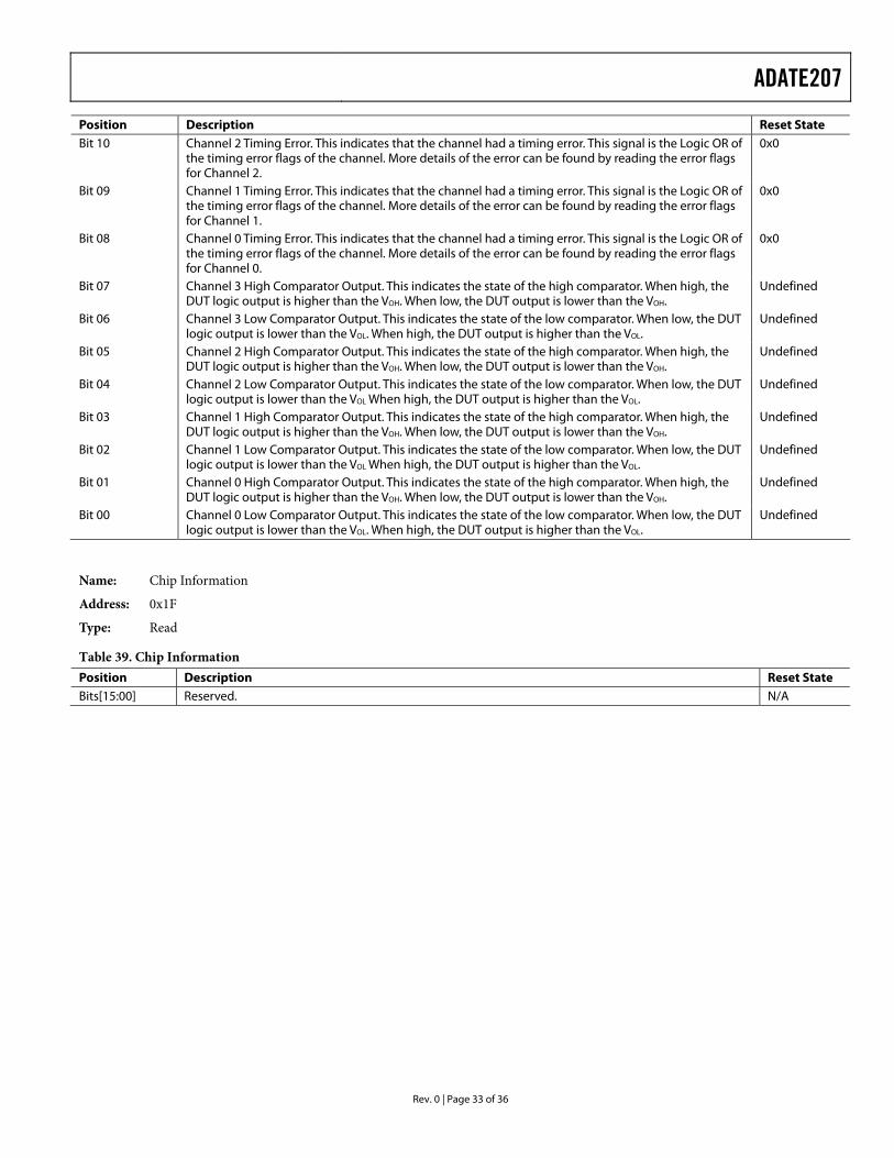
ADATE207
Rev. 0 | Page 33 of 36
Position Description Reset State Bit 10 Channel 2 Timing Error. This indicates that the channel had a timing error. This signal is the Logic OR of
the timing error flags of the channel. More details of the error can be found by reading the error flags for Channel 2.
0x0
Bit 09 Channel 1 Timing Error. This indicates that the channel had a timing error. This signal is the Logic OR of the timing error flags of the channel. More details of the error can be found by reading the error flags for Channel 1.
0x0
Bit 08 Channel 0 Timing Error. This indicates that the channel had a timing error. This signal is the Logic OR of the timing error flags of the channel. More details of the error can be found by reading the error flags for Channel 0.
0x0
Bit 07 Channel 3 High Comparator Output. This indicates the state of the high comparator. When high, the DUT logic output is higher than the VOH. When low, the DUT output is lower than the VOH.
Undefined
Bit 06 Channel 3 Low Comparator Output. This indicates the state of the low comparator. When low, the DUT logic output is lower than the VOL. When high, the DUT output is higher than the VOL.
Undefined
Bit 05 Channel 2 High Comparator Output. This indicates the state of the high comparator. When high, the DUT logic output is higher than the VOH. When low, the DUT output is lower than the VOH.
Undefined
Bit 04 Channel 2 Low Comparator Output. This indicates the state of the low comparator. When low, the DUT logic output is lower than the VOL When high, the DUT output is higher than the VOL.
Undefined
Bit 03 Channel 1 High Comparator Output. This indicates the state of the high comparator. When high, the DUT logic output is higher than the VOH. When low, the DUT output is lower than the VOH.
Undefined
Bit 02 Channel 1 Low Comparator Output. This indicates the state of the low comparator. When low, the DUT logic output is lower than the VOL When high, the DUT output is higher than the VOL.
Undefined
Bit 01 Channel 0 High Comparator Output. This indicates the state of the high comparator. When high, the DUT logic output is higher than the VOH. When low, the DUT output is lower than the VOH.
Undefined
Bit 00 Channel 0 Low Comparator Output. This indicates the state of the low comparator. When low, the DUT logic output is lower than the VOL. When high, the DUT output is higher than the VOL.
Undefined
Name: Chip Information
Address: 0x1F
Type: Read
Table 39. Chip Information Position Description Reset State Bits[15:00] Reserved. N/A
ADATE207
Rev. 0 | Page 34 of 36
APPLICATION INFORMATION TIME MEASUREMENT SUPPORT The ADATE207 contains support for time measurement through an external time measurement unit (TMU) in the following ways:
• Connect the high comparator output of any channel to TMU arm, TMU start, or TMU stop.
• Connect the low comparator output of any channel to TMU arm, TMU start, or TMU stop.
• Tristate the TMU multiplexer outputs using an enable control bit.
The time measurement unit select logic provides time and frequency measurement capability from any digital pin high or low comparator output. To accomplish this task, independent multiplexers are employed for directing the high or low comparator outputs of the digital pins to the (three) time measurement unit signals, TMU_ARM, TMU_START, and TMU_STOP. Off-chip control logic must select the appropriate TMU bus output signal from the ADATE207 devices on the board and direct its selection to the TMU.

ADATE207
Rev. 0 | Page 35 of 36
OUTLINE DIMENSIONS
0.10 MIN
0.700.600.50
1.000.800.60
COPLANARITY0.20
0.900.750.60 SEATING
PLANEBALL DIAMETER0.25 MIN
(4×)
DETAIL A1.70 MAX
1.27BSC
ABCDEFGHJKLMNPRTUVWY
13579111315192468101214161820
24.13BSC SQ BOTTOM
VIEW
A1 CORNERINDEX AREA
TOP VIEW
27.00BSC SQ
BALL A1INDICATOR
DETAIL A
17
COMPLIANT TO JEDEC STANDARDS MO-192-BAL-2 Figure 25. 256-Lead Ball Grid Array, Thermally Enhanced [BGA_ED]
(BP-256) Dimensions shown in millimeters
ORDERING GUIDE Model Temperature Range1 Package Description Package Option ADATE207BBP −25°C to +85°C 256-Lead Ball Grid Array, Thermally Enhanced [BGA_ED] BP-256 ADATE207BBPZ2 −25°C to +85°C 256-Lead Ball Grid Array, Thermally Enhanced [BGA_ED] BP-256 1 Guaranteed by design, not subject to production test. 2 Z = RoHS Compliant Part.

ADATE207
Rev. 0 | Page 36 of 36
NOTES
©2007 Analog Devices, Inc. All rights reserved. Trademarks and registered trademarks are the property of their respective owners. D05557-0-5/07(0)