Embed Size (px)
Citation preview
Qsys System Design Tutorial2015.05.04
TU-01006 Subscribe Send Feedback
This tutorial introduces you to the Qsys system integration tool available with the Quartus®II software.
This tutorial shows you how to design a system that uses various test patterns to test an external memorydevice. It guides you through system requirement analysis, hardware design tasks, and evaluation of thesystem performance, with emphasis on system architecture.
In this tutorial, you create a memory tester system that tests a synchronous dynamic random accessmemory (SDRAM) device. The final system contains the SDRAM controller and instantiates a Nios IIprocessor and embedded peripherals in a hierarchical subsystem. The final design includes various Qsyscomponents that generate test data, access memory, and verify the returned data.
The memory tester components for the design are Verilog HDL components with an accompanyingHardware Component Description File (_hw.tcl) that describes the interfaces and parameterization ofeach component. The _hw.tcl files are located in the tt_qsys_design\memory_tester_ip directory.
The final system contains the following components:
• Processor subsystem based on the Nios II/e core, which includes an on-chip RAM to store the process‐or's software code, and a JTAG UART to communicate via JTAG and display the memory test resultsin the host PC's console.
• SDRAM controller to control the off-chip DDR SDRAM device under test.• Custom and pseudo-random binary sequence (PRBS) pattern generators and checkers to test the
robustness of links.• Pattern select multiplexer and demultiplexer to choose between the two pattern generators and
checkers.• Pattern writer and reader that interact with the SDRAM controller.• Memory test controller.
Each section in this tutorial provides an overview describing the components that you instantiate. Youcan use the final system on hardware without a license, and perform the following actions with Altera'sfree OpenCore Plus evaluation feature:
• Simulate the behavior of the system and verify its functionality.• Generate time-limited device programming files for designs that incorporate Altera or partner IP.• Program a device and verify your design in hardware.
You can use the Nios II/e processor and the DDR SDRAM IP cores with a Quartus II subscription license.Design files for other development kit boards use different DDR SDRAM controllers to match thememory device available on the development kit.
© 2015 Altera Corporation. All rights reserved. ALTERA, ARRIA, CYCLONE, ENPIRION, MAX, MEGACORE, NIOS, QUARTUS and STRATIX words and logos aretrademarks of Altera Corporation and registered in the U.S. Patent and Trademark Office and in other countries. All other words and logos identified astrademarks or service marks are the property of their respective holders as described at www.altera.com/common/legal.html. Altera warrants performanceof its semiconductor products to current specifications in accordance with Altera's standard warranty, but reserves the right to make changes to anyproducts and services at any time without notice. Altera assumes no responsibility or liability arising out of the application or use of any information,product, or service described herein except as expressly agreed to in writing by Altera. Altera customers are advised to obtain the latest version of devicespecifications before relying on any published information and before placing orders for products or services.
ISO9001:2008Registered
www.altera.com101 Innovation Drive, San Jose, CA 95134

In this tutorial, you instantiate the complete memory tester system in the top-level system along with theprocessor IP Cores, which are grouped as their own processor system, and the SDRAM Controller IP. TheNios II processor includes a software program to control the memory tester system, which communicateswith the SDRAM Controller to access the off-chip SDRAM device under test.
Figure 1: Qsys Memory Tester
The components in the memory tester system are grouped into a single Qsys system with three majordesign functions. The design hierarchy allows you to instantiate the data pattern generator and datapattern checker components into separate systems. You can then add the memory tester system with thememory master and controller components.
Top-Level Qsys System
Memory TesterData Pattern Generator Memory Master and Controller Data Pattern Checker
ProcessorIP Cores
SDRAMController
SDRAMUnder Test
Custom Pattern Generator
PRBS Generator
Pattern Select (MUX)
Pattern WriterChecker
Select (DEMUX )
Test Controller PRBS Checker
Custom Pattern Checker
Nios II
Onchip RAM
(Code and Data)
Avalon-MM InterfaceAvalon-ST Interface
Pattern Reader
Pipeline Bridge
JTAG UART
Related InformationDownload and Install the Tutorial Design Files on page 3
AN320: OpenCore Plus Evaluation of Megafunctions
2 Qsys System Design TutorialTU-01006
2015.05.04
Altera Corporation Qsys System Design Tutorial
Send Feedback

Software and Hardware RequirementsThe Qsys System Design tutorial requires the following software and hardware requirements:
• Altera Quartus II software.• Nios II EDS.• tt_qsys_design.zip design files, available from the Qsys Tutorial Design Example page. The design
files include project files set up for select Altera development boards, and components that you can usein any Qsys design.
You can build the Qsys system in this tutorial for any Altera development board or your own customboard, if it meets the following requirements:
• An Altera Arria, Cyclone, or Stratix series FPGA.• Minimum of 12k logic elements (LEs).• Minimum of 128k of embedded memory.• JTAG connection to the FPGA that provides a communications link back to the host so that you can
monitor the memory test progress.• Any memory that has a Qsys-based controller with an Avalon® Memory-Mapped (Avalon-MM) slave
interface.
Related Information
• Altera Software Installation and Licensing Manual.• Qsys Tutorial Design Example• Qsys Tutorial Design Example (detailed diagram)
Download and Install the Tutorial Design Files1. On the Qsys Tutorial Design Example page, under Using this Design Example, click Qsys Tutorial
Design Example (.zip) to download and install the tutorial design files for the Qsys tutorial.2. Extract the contents of the archive file to a directory on your computer. Do not use spaces in the
directory path name.
In place of following all steps in this tutorial to create subsystem, hierarchical, and top-level design files,you can copy the completed design files listed below into the tt_qsys_design\quartus_ii_projects_for_boards\<development_board_type> directory, depending on your board type.
• The two completed subsystems: pattern_generator_system.qsys, and pattern_checker_system.qsysfrom the tt_qsys_design\completed_subsystems directory.
• The hierarchical system memory_tester_system.qsys from the tt_qsys_design\completed_subsystems\completed_memory_tester_system directory.
• The top-level hierarchical system top_system.qsys from the tt_qsys_design\quartus_ii_projects_for_boards\<development_board_type>\backup_and_completed_top_system\completed_top_system directory.
Related Information
• Qsys Tutorial Design Example• Qsys Tutorial Design Example (.zip)
TU-010062015.05.04 Software and Hardware Requirements 3
Qsys System Design Tutorial Altera Corporation
Send Feedback

• Detailed Diagram of the Memory Tester System
Open the Tutorial ProjectThe design files for the Qsys tutorial provide the custom IP design blocks that you need, and a partiallycompleted Quartus II project and Qsys system.
The following design requirements are included in the Qsys tutorial design files:
• Quartus II project I/O pin assignments and Synopsys Design Constraint (.sdc) timing assignments foreach supported development board.
• Parameterized Nios II processor core and software to communicate with the host PC that controls thememory test system that you develop.
• Parameterized DDR SDRAM controller to use the memory on the development board.
To open the tutorial project:
1. Open the Quartus II software.2. To open the Quartus II Project File (.qpf) for your board, click File > Open Project.3. Browse to the tt_qsys_design\quartus_ii_projects_for_boards\<development_board>\ directory.4. Select the relevant board-specific .qpf file, and then click Open.
Creating Qsys SystemsThe data pattern generator and data pattern checker are design blocks for the memory tester system. Inthis tutorial, you learn to instantiate, parameterize, and connect components by creating the data patterngenerator and data pattern checker Qsys systems.
• Data pattern generator—The data pattern generator generates high-speed streaming data, whichperforms either as a PRBS, or as a soft programmable sequence, for example, “walking ones.” Thedesign sends the data with an Avalon-Streaming (Avalon-ST) connection to the pattern writer of thememory master and control logic. The data pattern generator writes the data to memory based oncommands issued by the controller logic. When the design writes the data to memory, the patternreader logic reads the contents back and sends it to the data pattern verification logic.
• Data pattern checker—The data pattern checker accepts the data read back by the pattern reader froman Avalon-ST connection. The design verifies the data pattern to ensure that the pattern it writes tomemory is identical to the data that it reads back.
Create a Data Pattern Generator Qsys SystemThe data pattern generator includes two components to generate test patterns, and a third component tomultiplex the data that a processor controls. You configure the pattern generator to match the width ofthe memory interface. Because the data pattern generator provides a full word of data every clock cycle,configuring the components to match the memory width provides sufficient bandwidth to access thememory.
Note: As you add components and make connections in your Qsys system, error and warning messagesappear in the Qsys Messages tab, indicating steps that you must perform before the system iscomplete. Some error messages appear between steps and are not resolved immediately; as youprogress through the tutorial, errors are resolved, and the error messages disappear.
4 Open the Tutorial ProjectTU-01006
2015.05.04
Altera Corporation Qsys System Design Tutorial
Send Feedback

You must use the exact system names described in this tutorial in order for the provided scripts tofunction correctly.
Create a New Qsys System and Set up the Clock Source
1. In the Quartus II software, click Tools > Qsys to create a new Qsys design.2. In the System Contents tab, Qsys shows a clock source instance, clk_0. To open the clock source
settings, right-click clk_0, and then click Edit.3. Turn off Clock frequency is known to indicate that, when created, the higher-level hierarchical system
that instantiates this subsystem provides the clock frequency.4. Click Finish.5. Click File > Save As to save the Qsys system.6. In the Save As dialog box, type pattern_generator_system, and then click Save.
If Qsys prompts you to open the top_system.qsys file, click Cancel in the Open dialog box
Add a Pipeline BridgeThe components that make up the data pattern generator include several Avalon-MM slave interfaces. Toallow a higher-level system to access the Avalon-MM slave interfaces by reading and writing to a singleslave interface, you can consolidate the slave interfaces behind an Avalon-MM pipeline bridge, and exporta single Avalon-MM slave interface out of the system.
To determine the required address width for a bridge, you must know the required addresses span of theother components in the system. Memory-mapped component interfaces outside the system address eachinterface in the system by specifying a memory offset value relative to the base address of the bridge.
A pipeline bridge can also improve system timing performance by optionally adding pipeline registers tothe design.
1. In the Library search box, type bridge to filter the component list and show only bridge components.2. Select Avalon-MM Pipeline Bridge, and then click Add.3. In the parameter editor, under Parameters, type 11 for the Address width.
This width accommodates the memory span of all memory-mapped components behind the bridge inthis system. As you add the other components in the system, you specify their base addresses withinthe span of the address space.
4. Accept all other default settings, and then click Finish.The pipeline bridge is added to your system with the instance name mm_bridge_0.
5. On the System Contents tab, right-click mm_bridge_0, click Rename, and then type mm_bridge.6. In the Clock column for the mm_bridge clk interface, select clk_0 from the list.7. To export the mm_bridge s0 interface, double-click the Export column, and then type slave.
TU-010062015.05.04 Create a New Qsys System and Set up the Clock Source 5
Qsys System Design Tutorial Altera Corporation
Send Feedback
Add a Custom Pattern GeneratorThe pattern generator generates multiple test patterns to test the off-chip SDRAM device. The custompattern generator system provides a stream of pattern data via an Avalon-ST source interface.
The component is programmed with the pattern data and a pattern length. When the end of the pattern isreached, the custom pattern generator cycles back to the first element of the pattern. This custom patterngenerator generates the following standard memory tester patterns:
• Walking ones• Walking zeros• Low frequency• Alternating low frequency• High frequency• Alternating high frequency• Synchronous PRBS
The width of the memory dictates the walking ones or zeros pattern lengths. For example, when testing a32-bit memory, the walking ones or zeros pattern is 32 elements in length before repeating. The high andlow frequency patterns contain only two elements before repeating. The synchronous PRBS pattern is thelongest pattern containing 256 elements before repeating.
This custom pattern generator contains three interfaces, two of which control the generated pattern, and athird interface which control the behavior of the custom pattern generated. The processor accesses thepattern_access interface, which is write only, to program the elements of the custom pattern that are sentto the pattern writer core, and the csr interface, which is used for the control and status registers. Thest_pattern_output is the streaming source interface that sends data to the pattern writer core.
To add the custom pattern generator:
1. In the IP Catalog, expand Memory Test Microcores, and then double-click Custom PatternGenerator.
2. In the parameter editor, accept the default parameters, and then click Finish.3. Rename the instance to custom_pattern_generator.4. Set the custom_pattern_generator clock interface to clk_0.5. To connect the custom_pattern_generator csr interface to the mm_bridge m0 interface, in the
Connections column, click to fill in the connection dot between the custom_pattern_generator csrinterface and the mm_bridge m0 interface.
6. Connect the custom_pattern_generator pattern_access interface to the mm_bridge m0 interface.The processor accesses the system through the m0 interface to communicate with the csr andpattern_access interfaces.
7. To assign the custom_pattern_generator csr interface to a base address of 0400, in the Base column,double-click the 0x00000000 address, and then enter 400 for the base address, which is in hexadecimalformat.If the Base column is locked for the custom_pattern_generator csr, right-click and then click UnlockBase Address.
The address space represents memory accessible by the processor. Each address specifies a location inmemory that can be addressed and accessed, and each interface must have a unique address range. Theaddress space of each interface is determined by its base address and its memory span, or how muchmemory is required for that interface.
6 Add a Custom Pattern GeneratorTU-01006
2015.05.04
Altera Corporation Qsys System Design Tutorial
Send Feedback

You can see the default address range of the pattern_access interface in the Base and End columns on theSystem Contents tab.
You assign a base address for the csr interface that is higher than the end address of the pattern_accessinterface to avoid conflicting with the address space of the pattern_access interface.
Add a PRBS Pattern GeneratorThe output of the PRBS pattern generator is a statically-defined PRBS pattern. You can specify the patternlength before the pattern repeats in the parameter editor. The pattern length is defined by 2^(data width)– 1.
For example, a 32-bit PRBS pattern generator repeats the pattern after it sends 4,294,967,295 elements.You set the width of the PRBS generator based on the (local) data width of the memory on your board.
The PRBS pattern generator has two interfaces; the csr and the st_pattern_output streaming sourceinterface. The csr interface controls the behavior of the PRBS pattern generated. The st_pattern_outputstreaming source interface sends data to the pattern writer component.
1. In the IP Catalog, expand Memory Test Microcores, and then double-click PRBS Pattern Generator.2. In the parameter editor, accept the default parameters, and then click Finish.3. Rename the instance to prbs_pattern_generator.4. Set the prbs_pattern_generator clock interface to clk_0.5. Connect the prbs_pattern_generator csr interface to the mm_bridge m0 interface.6. Assign the prbs_pattern_generator csr interface to a base address of 0x0420, which is a base address
just higher than the end address of the custom_pattern_generator csr interface of 0x410.
Add a Two-to-One Streaming MultiplexerYou add a two-to-one streaming multiplexer between the pattern generators and the pattern writerbecause the system has two pattern sources, and the pattern writer component accepts data only from onestreaming source. The two-to-one streaming soft programmable multiplexer IP core allows the processorto select which pattern to send to the pattern writer.
The two-to-one streaming multiplexer component has the following interfaces:
• Two streaming inputs: st_input_A and st_input_B.• One streaming output: st_output.• One csr slave interface, which the processor controls to select whether input A or input B is sent to the
streaming output.
The custom pattern generator connects to input A, and the PRBS pattern generator connects to input B.
1. In the IP Catalog, expand Memory Test Microcores, and then double-click Two-to-one StreamingMux.
2. In the parameter editor, accept the default parameters, and then click Finish.3. Rename the instance to two_to_one_st_mux.4. Set the two_to_one_st_mux clock to clk_0.5. Connect the two_to_one_st_mux st_input_A interface to the custom_pattern_generator
st_pattern_output interface.6. Connect the two_to_one_st_mux st_input_B interface to the prbs_pattern_generator
st_pattern_output interface.
TU-010062015.05.04 Add a PRBS Pattern Generator 7
Qsys System Design Tutorial Altera Corporation
Send Feedback
7. Connect the two_to_one_st_mux csr interface to the mm_bridge m0 interface.8. Export the two_to_one_st_mux st_output interface with the name st_data_out.9. Assign the two_to_one_st_mux csr interface to a base address of 0x0440, which is a base address
higher than the end address of the prbs_pattern_generator csr interface at base address 0x0420
The output of the two-to-one streaming multiplexer carries the pattern data from either the custompattern generator or the PRBS pattern generator, to the pattern writer. The data, from the output of thetwo-to-one streaming multiplexer, achieves a throughput of one word per clock cycle.
Verify the Memory Address Map
You control the system by accessing the memory locations allocated to each component within thesubsystem. To ensure that the memory map of the system you create matches the memory map of othercomponents, you must verify the base addresses for the data pattern generator system.
On the Address Map tab, verify that the entries in the Address Map table match the values in #mwh1411073373020/table_54ED964DACCD4D7480A621FF0B0D0E00. Red exclamation marksindicate that the address ranges overlap. Correct the base addresses, as appropriate, to ensure there are nooverlapping addresses, and your map matches this tutorial’s guidelines.
Table 1: Address Map Table
Component Address
custom_pattern_generator.csr 0x00000400 – 0x0000040f
custom_pattern_generator.pattern_access 0x00000000 – 0x000003ff
prbs_pattern_generator.csr 0x00000420 – 0x0000043f
two_to_one_st_mux.csr 0x00000440 – 0x00000447
Connect the Reset Signals
You must connect all the reset signals, which eliminates the error messages in the Messages tab. Qsysallows multiple reset domains, or one reset signal for the system. In the design, you want to connect all thereset signals with the incoming reset signal. To connect all the reset signals, on the System menu, selectCreate Global Reset Network.
At this point in the system design, Qsys shows no remaining error messages. If you have any errormessages in the Messages tab, review the procedures to create this system to ensure you did not miss astep. You can view the reset connections and the timing adapters on the System Contents tab, and byselecting Show System With Qsys Interconnect on the System menu.
Save the System
At this point, there should be no remaining error messages in the Messages tab, and the system iscomplete. Save the system.
Create a Data Pattern Checker Qsys SystemThe data pattern checker system receives a pattern from SDRAM and verifies it against the pattern fromthe data pattern generator. The pattern reader sends the data to a one-to-two streaming demultiplexerthat routes the data to either the custom pattern checker or the PRBS pattern checker. The one-to-two
8 Verify the Memory Address MapTU-01006
2015.05.04
Altera Corporation Qsys System Design Tutorial
Send Feedback

streaming demultiplexer is soft programmable so that the processor can select which pattern checker IPcore should verify the data that the pattern reader reads. The custom pattern checker is also soft program‐mable and is configured to match the same pattern as the custom pattern generator.
Refer to the Qsys Memory Tester figure for a graphical description.
Related InformationQsys System Design Tutorial on page 1
Create a New Qsys System and Set Up the Clock Soource
1. In the Quartus II software, click Tools > Qsys to create a new Qsys design.2. In the System Contents tab, Qsys shows a clock source instance, clk_0. To open the clock source
settings, right-click clk_0, and then click Edit.3. Turn off Clock frequency is known to indicate that, when created, the higher-level hierarchical system
that instantiates this subsystem provides the clock frequency.4. Click Finish.5. Click File > Save As to save the Qsys system.6. In the Save As dialog box, type pattern_checker_system, and then click Save.
Add a Pipeline Bridge
1. In the Library search box, type bridge to filter the component list and show only bridge components.2. Select Avalon-MM Pipeline Bridge, and then click Add.3. In the parameter editor, under Parameters, type 11 for the Address width.
This width accommodates the memory span of all memory-mapped components behind the bridge inthis system. As you add the other components in the system, you specify their base addresses withinthe span of the address space.
4. Accept all other default settings, and then click Finish.The pipeline bridge is added to your system with the instance name mm_bridge_0.
5. On the System Contents tab, right-click mm_bridge_0, click Rename, and then type mm_bridge.6. In the Clock column for the mm_bridge clk interface, select clk_0 from the list.7. To export the mm_bridge s0 interface, double-click the Export column, and then type slave.
Add a Custom Pattern CheckerThe custom pattern checker performs the opposite operation of the custom pattern generator. It has astreaming input interface, st_pattern_input, that accepts data from the one-to-two streamingdemultiplexer. The processor uses the Avalon-MM csr slave interface to control the component. Thecustom packet checker also has a memory-mapped slave interface, pattern_access, that the processor usesto program the same patterns as the custom pattern generator component.
1. In the IP Catalog, expand Memory Test Microcores, and then double-click Custom Pattern Checker.2. In the parameter editor, accept the default parameters, and then click Finish.3. Rename the instance to custom_pattern_checker.4. Set the custom_pattern_checker clock to clk_0.5. Connect the custom_pattern_checker csr interface to the mm_bridge m0 interface.6. Connect the custom_pattern_checker pattern_access interface to the mm_bridge m0 interface.7. Assign the custom_pattern_checker csr interface to a base address of 0x0420.8. Maintain the custom_pattern_checker pattern_access interface base address of 0x0000.
TU-010062015.05.04 Create a New Qsys System and Set Up the Clock Soource 9
Qsys System Design Tutorial Altera Corporation
Send Feedback
Add the PRBS Pattern CheckerThe PRBS pattern checker performs the opposite operation of the PRBS pattern generator. The processoruses the memory-mapped csr slave interface to control the component. The st_pattern_input streaminginput accepts data from the one-to-two streaming demultiplexer.
1. In the IP Catalog, expand Memory Test Microcores, and then double-click PRBS Pattern Checker.2. In the parameter editor, accept the default parameters, and then click Finish.3. Rename the instance to prbs_pattern_checker.4. Set the prbs_pattern_checker clock to clk_0.5. Connect the prbs_pattern_checker csr interface to the mm_bridge m0 interface.6. Assign the prbs_pattern_checker csr interface to a base address of 0x0440.
Add a One-to-Two Streaming DemultiplexerThe one-to-two streaming demultiplexer performs the opposite operation of the two-to-one streamingmultiplexer. It has a streaming input interface, st_input, that accepts data from the pattern reader, andtwo streaming output interfaces, st_output_A and st_output_B, that connect to the custom patterngenerator and PRBS pattern generator. To allow the processor to program the data route through thecomponent, the system includes the slave interface, csr.
1. In the IP Catalog, expand Memory Test Microcores, and then double-click One-to-two StreamingDemux.
2. In the parameter editor, accept the default parameters, and then click Finish.3. Rename the instance to one_to_two_st_demux.4. Set the one_to_two_st_demux clock to clk_0.5. Export the one_to_two_st_demux st_input interface with the name st_data_in.6. Connect the one_to_two_st_demux csr interface to the mm_bridge m0 interface.7. Assign the one_to_two_st_demux csr interface to a base address of 0x0400.8. Connect the custom_pattern_checker st_pattern_input interface to the one_to_two_st_demux
st_output_A interface.9. Connect the prbs_pattern_checker st_pattern_input interface to the one_to_two_st_demux
st_output_B interface.
Verify the Memory Address Map
On the Address Map tab, verify that the entries in the Address Map table match the values in #mwh1411073373020/table_54ED964DACCD4D7480A621FF0B0D0E00. Red exclamation marksindicate that the address ranges overlap. Correct the base addresses, as appropriate, to ensure there are nooverlapping addresses, and your map matches this tutorial’s guidelines.
Table 2: Address Map Table
Component Address
one_to_two_st_demux.csr 0x00000400 - 0x00000407
custom_pattern_checker.csr 0x00000420 - 0x0000042f
custom_pattern_checker.pattern_access 0x00000000 - 0x000003ff
prbs_pattern_checker.csr 0x00000440 - 0x0000045f
10 Add the PRBS Pattern CheckerTU-01006
2015.05.04
Altera Corporation Qsys System Design Tutorial
Send Feedback
Connect the Reset Signals
You must connect all the reset signals, which eliminates the error messages in the Messages tab. Qsysallows multiple reset domains, or one reset signal for the system. In the design, you want to connect all thereset signals with the incoming reset signal. To connect all the reset signals, on the System menu, selectCreate Global Reset Network.
At this point in the system design, Qsys shows no remaining error messages. If you have any errormessages in the Messages tab, review the procedures to create this system to ensure you did not miss astep. You can view the reset connections and the timing adapters on the System Contents tab, and byselecting Show System With Qsys Interconnect on the System menu.
Save the System
At this point, there should be no remaining error messages in the Messages tab, and the system iscomplete. Save the system.
Assemble a Hierarchical SystemHierarchical systems allow you to reuse modular system components. Additionally, hierarchical systemsallow you to break large systems into smaller subsystems thus, creating more manageable designs.
The memory tester design includes the following lower-level subsystems:
• Data pattern generator—Generates and transmits Avalon-ST data to the memory tester components.• Data pattern checker—Receives and verifies Avalon-ST data from the memory tester components.
TU-010062015.05.04 Connect the Reset Signals 11
Qsys System Design Tutorial Altera Corporation
Send Feedback
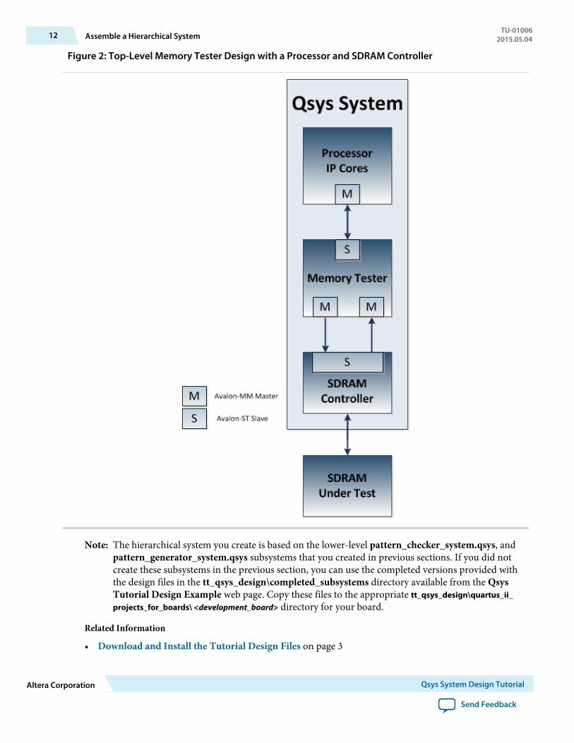
Figure 2: Top-Level Memory Tester Design with a Processor and SDRAM Controller
Note: The hierarchical system you create is based on the lower-level pattern_checker_system.qsys, andpattern_generator_system.qsys subsystems that you created in previous sections. If you did notcreate these subsystems in the previous section, you can use the completed versions provided withthe design files in the tt_qsys_design\completed_subsystems directory available from the QsysTutorial Design Example web page. Copy these files to the appropriate tt_qsys_design\quartus_ii_projects_for_boards\ <development_board> directory for your board.
Related Information
• Download and Install the Tutorial Design Files on page 3
12 Assemble a Hierarchical SystemTU-01006
2015.05.04
Altera Corporation Qsys System Design Tutorial
Send Feedback

• Create a Data Pattern Generator Qsys System on page 4• Create a Data Pattern Checker Qsys System on page 8• Qsys Tutorial Design Example
Create the Hierarchical Memory Tester SystemThe memory tester system includes several slave interfaces. However, the memory tester groups theinterfaces behind a pipeline bridge that exports a single slave interface to the top-level system. Thistechnique allows the top-level system to access all of the memory-mapped slave ports by reading andwriting to a single pipeline bridge slave interface. The bridge also adds a level of pipelining, which canimprove timing performance.
Figure 3: Memory Tester Design Interface
M
S
Sr
Sk
Avalon-MM Master
Avalon-MM Slave
Avalon-ST Source
Avalon-ST Sink
M
S
Pipeline Bridge
Sr
S
Pattern GeneratorSubsystem
Sk
S
Data CheckerSubsystem
Sr
S
RAM TestController
Sr
M
Sk
PatternReader
Sr
M
Sk
PatternWriter
Sk
Avalon-MM Interface
Avalon-ST Interface
Legend
Memory MasterComponents
TU-010062015.05.04 Create the Hierarchical Memory Tester System 13
Qsys System Design Tutorial Altera Corporation
Send Feedback

1. In Qsys, create a new system called, memory_tester_system.2. For the clk instance, turn off Clock frequency is known to indicate that the higher-level hierarchical
system that instantiates this subsystem provides the clock frequency.3. In the IP Catalog, select the Avalon-MM Pipeline Bridge to add to your Qsys system.4. For the Avalon-MM Pipeline Bridge, in the parameter editor, type 13 for the Address width.
To accommodate for the address translation from master to slave, that is a byte address as the input,and a word address (4 bytes) as the output, the address width increases from 11.
5. Rename the instance to mm_bridge.6. Set the mm_bridge_clk interface to clk_0.7. Export the mm_bridge s0 interface with the name slave.
Add the Pattern GeneratorThe custom pattern generator system provides a stream of pattern data via an Avalon-ST source interface.You control the system by accessing the memory locations allocated to each component within thesubsystem. The system connects slave ports to a pipeline bridge, which it then exposes outside of thesystem.
The pattern generator system contains the following components:
• Pipeline bridge• Custom pattern generator• PRBS pattern generator• Two-to-one streaming multiplexer• Streaming timing adapters
1. In the IP Catalog, under Project expand System, and then double-click pattern_generator_system.2. In the parameter editor, click Finish to accept the default settings.3. Rename the instance to pattern_generator_subsystem.4. Set the pattern_generator_subsystem clk to clk_0.5. Connect the pattern_generator_subsystem slave interface to the mm_bridge m0 interface.6. Connect the pattern_generator_subsystem reset interface to the clk_0 clk_reset interface.
Add the Pattern CheckerThe pattern checker system validates data that arrives via an Avalon-ST sink interface. You control thesystem by accessing the memory locations allocated to each component within the subsystem. The systemconnects all of the slave ports to a pipeline bridge, which it then exposes outside of the system.
The pattern checker system contains the following components:
• Pipeline bridge• Custom pattern checker• PRBS pattern checker• One-to-two demultiplexer
14 Add the Pattern GeneratorTU-01006
2015.05.04
Altera Corporation Qsys System Design Tutorial
Send Feedback
1. In the IP Catalog, double-click pattern_checker_system from the System group.2. In the parameter editor, click Finish to accept the default settings.3. Rename the instance to pattern_checker_subsystem.4. Set the pattern_checker_subsystem clk to clk_0.5. Connect the pattern_checker_subsystem slave interface to the mm_bridge m0 interface.6. Connect the pattern_checker_subsystem reset interface to the clk_0 clk_reset interface.
Add Memory Master Components
Memory masters access the SDRAM controller by writing the test pattern to the memory and reading thepattern back for validation. The RAM test controller accepts commands from the processor and controlsthe memory masters. Each command contains a start address, test length in bytes, and memory block sizein bytes. The RAM test controller segments the commands into smaller block transfers and issues thecommands to the read and write masters independently via streaming connections.
When the pattern reader or writer components complete a block transfer, they signal to the RAM testcontroller that they are ready for another command. The RAM test controller issues the block-sizedcommands independently, which minimizes the number of idle cycles between memory transfers. TheRAM test controller also ensures that the pattern reader never overtakes the pattern writer with respect tothe memory locations it is testing, otherwise data corruption occurs.
The SDRAM controller is parameterized to use a local maximum burst length of 2. The pattern reader andwriter components are also configured to match this burst length to maximize the memory bandwidth.
Add a Pattern Writer ComponentThe pattern writer component accepts memory transfer commands from the RAM test controller with thecommand streaming interface. The st_data streaming interface accepts data provided by the design’spattern generator. The mm_data memory-mapped interface writes the pattern data to the SDRAMcontroller.
Before you begin
1. In the IP Catalog, double-click Pattern Writer from the Memory Test Microcores group.2. In the parameter editor, turn on Burst Enable.3. Ensure that the Maximum Burst Count is 2.4. Ensure that Enable Burst Re-alignment is turned on.5. To accept the other default parameters, click Finish.6. Rename the instance to pattern_writer.7. Set the pattern_writer clock to clk_0.8. Connect the pattern_writer st_data interface to the pattern_generator_subsystem st_data_out
interface.9. Export the pattern_writer mm_data interface with the name write_master.
Add a Pattern Reader ComponentThe pattern reader component accepts memory transfer commands from the RAM test controller withthe command streaming interface. The mm_data interface reads the pattern data from the SDRAMcontroller. The st_data interface sends the data read from memory to the design’s pattern checker.
TU-010062015.05.04 Add Memory Master Components 15
Qsys System Design Tutorial Altera Corporation
Send Feedback
1. In the IP Catalog, double-click Pattern Reader from the Memory Test Microcores group.2. n the parameter editor, turn on Burst Enable.3. Ensure the Maximum Burst Count is 2.4. Ensure that Enable Burst Re-alignment is turned on.5. To accept the other default parameters, click Finish.6. Rename the instance to pattern_reader.7. Set the pattern_reader clock to clk_0.8. Connect the pattern_reader st_data interface to the pattern_checker_subsystem st_data_in
interface.9. Export the pattern_reader mm_data interface with the name read_master.
Add a RAM Test ControllerThe RAM test controller contains two streaming command interfaces; write_command andread_command, that send commands to the pattern reader and pattern writer components. Thesestreaming interfaces issue commands effectively because Avalon-ST interfaces offer low latency and asimple handshaking protocol, as well as because the processor accesses a slave port, csr, to writecommands to the controller.
1. In the IP Catalog, double-click RAM Test Controller from the Memory Test Microcores group.2. In the parameter editor, click Finish to accept the default parameters.3. Rename the instance to ram_test_controller.4. Set the ram_test_controller clock to clk_0.5. Connect the ram_test_controller write_command interface to the pattern_writer_command
interface.6. Connect the ram_test_controller read_command interface to the pattern_reader_command
interface.7. Connect the ram_test_controller csr interface to the mm_bridge m0 interface.
Do not use the Generation tab at this point in the tutorial to generate HDL code for these subsystems. Youmust generate files for the entire top-level system, which includes all the subsystems. The batch scriptprovided for you to program the device requires that only one system is generated in the project directory.The top-level design includes a Nios II subsystem, and the Nios II software build tools require the SOPCInformation File (.sopcinfo) to be generated for the top-level design. If there are multiple .sopcinfo files,the batch script to program the device fails with an error from the software build tools.
Connect the Reset Signals
You must connect all the reset signals, which eliminates the error messages in the Messages tab. Qsysallows multiple reset domains, or one reset signal for the system. In the design, you want to connect all thereset signals with the incoming reset signal. To connect all the reset signals, on the System menu, selectCreate Global Reset Network.
At this point in the system design, Qsys shows no remaining error messages. If you have any errormessages in the Messages tab, review the procedures to create this system to ensure you did not miss astep. You can view the reset connections and the timing adapters on the System Contents tab, and byselecting Show System With Qsys Interconnect on the System menu.
16 Add a RAM Test ControllerTU-01006
2015.05.04
Altera Corporation Qsys System Design Tutorial
Send Feedback

Verify the Memory Address Map
To ensure that the memory map of the system you create matches the memory map of other components,you must verify the base addresses for the memory tester system. In Qsys, on the Address Map tab, verifythat the entries in Address Map table match the values in Table 3. Red exclamation marks indicate thatthe address ranges overlap. Correct the base addresses, as appropriate, to ensure there are no overlappingaddresses.
Table 3: Address Map Table
Component Base Address Address
mm_bridge_0.s0 N/A N/A
pattern_generator_subsystem.slave 0x0 0x00000000 – 0x000007ff
pattern_checker_subsystem.slave 0x1000 0x0001000 – 0x000017ff
ram_test_controller.csr 0x800 0x00000800 – 0x0000081f
Save the System
At this point, there should be no remaining error messages in the Messages tab, and the system iscomplete. Save the system.
Complete the Top-Level System1. In Qsys, open the top_system.qsys file from the tt_qsys_design\quartus_ii_projects_for_boards\<develop‐
ment_board> directory.The top-level system is set up for your development board, with an external clock source, a processorsystem, and an SDRAM controller. You can view the clocks in top-level system on the Clock Settingstab, and the partially-completed system connections on the System Contents tab.
2. In the IP Catalog, double-click memory_tester_system from the System group.3. Click Finish to accept the default parameters, and to add the memory tester system to the top-level
system.4. Rename the system to memory_tester_subsystem.5. On the System Contents tab, use the arrows to move the memory_tester_subsystem up between the
cpu_subsystem and the sdram.Since the cpu_subsystem controls the memory_tester_subsystem, and thememory_tester_subsystem controls the sdram, this positioning allows you to more easily visualizesystem performance.
6. Set the memory_tester_subsystem clk to either the sdram_sysclk (for ALTMEMPHY-based designs),or sdram_afi_clk (for UniPHY-based designs).Some boards have an FPGA and SDRAM device that use either the Altera DDR or DDR2 SDRAMController with ALTMEMPHY; others use the Altera DDR3 SDRAM controller with UniPHY.
7. Connect the memory_tester_subsystem reset interface to the ext_clk clk_reset interface.8. Connect the memory_tester_subsystem reset interface to the cpu_subsystem cpu_jtag_debug_reset
interface.This design exports the Nios II processor JTAG debug reset output interface,jtag_debug_module_reset, from the cpu_subsystem with the interface name cpu_ jtag_debug_reset.The design must connect this Nios II reset output to any component reset inputs that require resetting
TU-010062015.05.04 Verify the Memory Address Map 17
Qsys System Design Tutorial Altera Corporation
Send Feedback
by the Nios II processor code or JTAG interface, and also to the Nios II processor's reset inputinterface. The cpu_subsystem cpu_reset interface connects to the Nios II processor's reset inputinterface. The top_level.qsys file connects the cpu_jtag_debug_reset interface to the cpu_resetinterface.
9. Connect the memory_tester_subsystem write_master and read_master interfaces to either thesdram s1 interface (for ALTMEMPHY-based designs), or sdram avl interface (for UniPHY-baseddesigns).
10.Connect the memory_tester_subsystem slave interface to the cpu_subsystem master interface.11.Maintain the base addresses of 0x0 for the memory_tester_subsystem slave interface, and for either
the sdram s1 interface (for ALTMEMPHY-based designs), or sdram avl interface (for UniPHY-baseddesigns).
The two slave interfaces can use the same address map range because different masters control them. Thecpu_subsystem master interface controls the memory_tester_subsystem, and thememory_tester_subsystem write_master and read_master interfaces control the sdram interface.
Viewing the Memory Tester System in QsysYou can use the Hierarchy tab, accessed from the View menu, to show the complete hierarchy of yourdesign. The Hierarchy tab is a full system hierarchical navigator, which expands the system contents toshow modules, interfaces, signals, contents of subsystems, and connections. The graphical interface of theHierarchy tab displays a unique icon for each element represented in the system, including interfaces,directional pins, IP blocks, and system icons that show exported interfaces and the instances ofcomponents that make up a system.
Click Generate > HDL Example to view the HDL for an example instantiation of the system. The HDLexample lists the signals from the exported interfaces in the system. The signal names are the exportedinterface name followed by an underscore, and then the signal name specified in the component or IPcore. Most of the signals connect to the external SDRAM device.
Compiling and Downloading Software to a Development Board
Before you begin
Altera recommends that you download the memory tester system to a development board to complete thedesign process and test the memory interface of the board. If you do not have a development board youcan follow the steps provided in the accompanying readme.txt file to learn more details about portingdesigns to FPGA devices or boards.
The Altera-provided software tests the memory using various test parameters and patterns, and is scriptedfor compilation and download to the board.
1. To download the top-level system to a development board, in Qsys, click Generate > Generate.2. Select the language for Create HDL design files for synthesis, and turn off the option to create a Block
Symbol File (.bsf).3. Click Generate. Qsys generates HDL files for the system and the Quartus II IP File (.qip) that provides
the list of required HDL files for the Quartus II compilation.4. When Qsys completes the generation, click Close.
18 Viewing the Memory Tester System in QsysTU-01006
2015.05.04
Altera Corporation Qsys System Design Tutorial
Send Feedback

5. In the Quartus II software, on the Project menu, click Add/Remove Files in Project and verify that thenewly-generated .qip file, top_system.qip, and the timing constraints file, my_constraints.sdc appearin the Files list.
6. Click Processing > Start Compilation. When compilation completes, click OK.7. Connect the development board to a supported programming cable.8. Click Tools > Nios II Command Shell [gcc4].9. Type the following command to emulate your local c:/ drive for your Windows environment: cd /
cygdrive/c/.10.Navigate to the quartus_ii_projects_for_boards\<development_board>\software directory.11.Type the following command at the Nios II command Shell: ./batch_script.sh.
The batch script compiles the Nios II software and downloads the SRAM Object File (.sof) program‐ming file to the FPGA.
The terminal window shows messages indicating the progress. If you see error messages related to theJTAG chain, check your programming cable installation and board setup to ensure that it is set upcorrectly.
After the script configures the FPGA, it downloads the compiled Nios II software to the board andestablishes a terminal connection with the board. The test software performs test sweeps on the SDRAMby varying the following parameters:
• Pattern type• Memory block size• Memory block trail distance (number of blocks by which the pattern reader trails the pattern writer)• Memory span tested
Ensure that you have only one set of generated system files in the project directory, otherwise the batchscript to program the device fails with an error from the software build tools.
The memory throughput values appear in the command terminal as the memory is tested. These valuesare reported in hexadecimal and represent the number of clock cycles required to test the entire SDRAMaddress span. The output is restricted to hexadecimal due to a small software library that prints thecharacters to the terminal. Because the memory tester system writes to the memory and then reads it back,the number of bytes it accesses and reports in the transcript window is double the memory span. Thisnumber varies depending on the span of memory being tested for your memory device. Knowing the datawidth of the memory interface, the number of bytes transferred, and the number of clock cycles for thetransfer, you can determine the memory access efficiency.
The SDRAM controller in the top-level Qsys system has a 32-bit local interface width, therefore memorydata width in bytes is 4 bytes for the tutorial design.
Efficiency = 100 × total bytes transferred/(memory data width in bytes × total clock cycles)
The memory test runs until the design finishes testing the complete memory. To end the test early, typeCtrl+C in the command window. To calculate the efficiency for the last throughput numbers in, convertthe hexadecimal numbers to decimal, as follows:
• 0x4000000 bytes transferred is 0d67108864 total bytes transferred• 0x107d856 clock cycles is 0d17291350 total clock cycles
Therefore, the efficiency for this example is:
100 × 67108864 / (4 × 17291350) = 97.0%
TU-010062015.05.04 Compiling and Downloading Software to a Development Board 19
Qsys System Design Tutorial Altera Corporation
Send Feedback
Related InformationDownload and Install the Tutorial Design Files on page 3
Debugging Your DesignIf the memory test starts but does not complete successfully, the terminal displays failure messages. If yousee failure messages from the memory test, review the previous sections and check that you havecompleted all of the instructions in this tutorial successfully. A missed connection or incorrect memoryaddress assignment may cause the tester design to fail on the board.
Altera provides completed systems, so that you can verify your system designs. You can copy thecompleted systems into the project directory with different names, so that you can open two differentinstances of Qsys for a side-by-side comparison. Alternatively, you can replace your systems with theprovided completed systems to run the memory tester design successfully.
Related InformationDownload and Install the Tutorial Design Files on page 3
Verifying Hardware in System ConsoleYou can use the Quartus II System Console to verify your system design. The design example files includescripts that exercise your system using System Console Tcl commands. The example uses a JTAG-to-Avalon Master Bridge component to drive the slave components, instead of a Nios II processor system.
The \quartus_ii_projects_for_boards\<development_board>\system_console directory contains therun_sweep.tcl, base_address.tcl, and test_cases.tcl scripts. You use these scripts to set up and runmemory tests on the development board projects. You can view the scripts to help you understand theSystem Console commands that drive the slave component registers. The scripts work with any board, ifyou keep the same Qsys system structure.
The run_sweep.tcl file is the main script, which calls the other two scripts. The base_address.tcl file includesinformation about the base addresses of the slave components from the previous chapters. If you changethe base addresses of the slave components, you must also change the addresses in the base_address.tcl file.The test_cases.tcl file includes settings for memory span, memory block sizes, and memory block traildistance.
The run_sweep.tcl file contains Tcl commands for the following actions:
• Initialize the components• Adjust test parameters• Start the PRBS pattern checker, PRBS pattern generator, and RAM controller• Continuously poll the stop and fail bits in the PRBS checker
Related InformationDownload and Install the Tutorial Design Files on page 3
Open the Tutorial ProjectYou can use completed design files in the tt_qsys_design\quartus_ii_projects_for_boards\<development_board>directory.
20 Debugging Your DesignTU-01006
2015.05.04
Altera Corporation Qsys System Design Tutorial
Send Feedback

1. Open the Quartus II project in the project directory for your development board type.2. In Qsys, open top_system.qsys in the project directory for your development board type.
Add the JTAG-to-Avalon Master BridgeThe JTAG-to-Avalon master bridge acts as a bridge between the JTAG interface and the system's memorytester.
1. In the IP Catalog select JTAG to Avalon Master Bridge, and then click Add.2. In the parameter editor, click Finish to accept the default parameters.3. Rename the instance to jtag_to_avalon_bridge.4. Connect the jtag_to_avalon_bridge master interface to the memory_tester_subsystem slave
interface.5. Set the jtag_to_avalon_bridge clk domain to sdram_sysclk.6. Connect the jtag_avalon_bridge clk_reset interface to the ext_clk clk_reset interface.7. Connect the jtag_avalon_bridge clk_reset interface to either the sdram reset_request_n interface (for
ALTMEMPHY-based designs), or sdram afi_reset interface (for UniPHY-based designs).8. Connect the jtag_avalon_bridge master_reset interface to the memory_tester_subsystem reset
interface, and to either the sdram soft_reset_n interface (for ALTMEMPHY-based designs), or sdramsoft_reset interface (for UniPHY-based designs).
9. To disable the cpu_subsystem system, in the Use column, turn off Use, since you are replacing itsfunction with the bridge and System Console.
10.Save the jtag_to_avalon_bridge system.
Debug with System ConsoleThe design example scripts test the memory in loops for different block sizes, that is, the number of bytesto group together in a single instance of back-to-back reads or writes. The scripts also test the memory inloops for different memory block trails, that is, the number of blocks by which the pattern reader trails thepattern writer.
1. To download the programming file to your development board, in Qsys, click Generate > Generate.2. Select the language for Create HDL design files for synthesis.3. Click Generate. Qsys generates HDL files for the system and the .qip file, which provides the list of
required HDL files for the Quartus II compilation.4. When Qsys completes the generation, click Close.5. In the Quartus II software, click Project > Add/Remove Files in Project, and verify that the project
contains the top_system.qip.6. Click Processing > Start Compilation. When compilation completes, click OK.7. Connect the development board to a supported programming cable.8. Click Tools > Programmer.9. Check that the Programmer displays the correct programming hardware. Otherwise, click Hardware
Setup and select the correct programming hardware, and then click Close.10.To program the device, click Start.
TU-010062015.05.04 Add the JTAG-to-Avalon Master Bridge 21
Qsys System Design Tutorial Altera Corporation
Send Feedback
11.In Qsys, click Tools > System Console.12.Before you execute scripts in System Console, navigate to the directory for the Tcl scripts, and then in
Qsys System Console window, click File > Execute Script.13.To start the memory tests, run the run_sweep.tcl file from the tt_qsys_design\quartus_ii_projects_for_
boards\<development_board> \system_console directory.When you run the run_sweep.tcl script, the System Console displays the progress of the tests in theMessages tab. The tests perform test sweeps on the SDRAM by varying the memory block size andmemory block trail distance. When the tests finish successfully, Qsys generates a message that reportssuccessful completion.
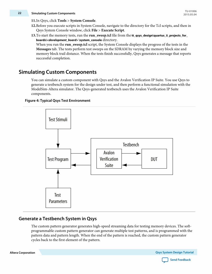
Simulating Custom ComponentsYou can simulate a custom component with Qsys and the Avalon Verification IP Suite. You use Qsys togenerate a testbench system for the design under test, and then perform a functional simulation with theModelSim-Altera simulator. The Qsys-generated testbench uses the Avalon Verification IP Suitecomponents.
Figure 4: Typical Qsys Test Environment
AvalonVerification
SuiteDUTTest Program
Testbench
Test Parameters
Test Stimuli
Generate a Testbench System in QsysThe custom pattern generator generates high-speed streaming data for testing memory devices. The soft-programmable custom pattern generator can generate multiple test patterns, and is programmed with thepattern data and pattern length. When the end of the pattern is reached, the custom pattern generatorcycles back to the first element of the pattern.
22 Simulating Custom ComponentsTU-01006
2015.05.04
Altera Corporation Qsys System Design Tutorial
Send Feedback
If you do not want to use the Qsys-generated testbench system, you can create your own Qsys testbenchsystem by adding the Avalon Verification Suite Bus Functional Models (BFMs) or your own models forsimulation. You can also generate a Qsys simulation model for the design or Qsys system under test, anduse your own custom HDL testbench to provide the simulation stimulus.
Related InformationDownload and Install the Tutorial Design Files on page 3
Create a New Qsys System for the Design Under Test
1. In the Quartus II software, open the Quartus II Project File, qsys_sim_tutorial.qpf, from the\simulation_tutorial directory.
2. In Qsys, click File > New System to create a new Qsys design.3. To remove the clock source, which is not needed for this design, right-click clk_0, and then click
Remove.4. In the IP Catalog, select Custom Pattern Generator from the Memory Test Microcores group, and
then click Add.5. In the parameter editor, click Finish to accept the default parameters.6. Rename the instance to pg to provide a short instance name for the pattern generator.
Export Design Under Test
1. In Qsys, on the System Contents tab, in the Export column, for each interface click Double-click toexport, and maintain the default export names.
2. Save the system as pattern_generator.
Generate a Testbench System
1. In Qsys click Generate > Generate Testbench System.2. Under Testbench System, for Create testbench Qsys system, select Standard, BFMs for standard
Qsys interfaces.3. Under Synthesis, select None for Create HDL design files for synthesis, and turn off Create block
symbol file (.bsf).4. Click Generate.5. After Qsys generates the testbench, click Close.
Qsys generates this testbench system in the \simulation_tutorial\pattern_generator\testbench directory.
You can generate the simulation model for the Qsys testbench system at the same time by turning onCreate testbench simulation model. However, the Qsys-generated testbench system's components namesare assigned automatically and you may want to control the instance names to make it easier to run thetest program for the BFMs. In this tutorial, you edit the Qsys testbench system before generating thesimulation model.
Generate Testbench System's Simulation ModelsIn this section, you open the generated Qsys testbench system and rename the BFM component instancenames to ensure the testbench names match the test program provided with the tutorial design files.Additionally, you generate the testbench's simulation model.
TU-010062015.05.04 Create a New Qsys System for the Design Under Test 23
Qsys System Design Tutorial Altera Corporation
Send Feedback

1. In Qsys, open the testbench system, pattern_generator_tb.qsys, from the simulation_tutorial\pattern_generator\testbench directory.
2. On the System Contents tab, rename the instance as they appear in Table 5–1.Qsys-Generated Components' Names New Instance Name
pattern_generator_inst DUT
pattern_generator_inst_pg_clock_bfm clock_source
pattern_generator_inst_pg_reset_bfm reset_source
pattern_generator_inst_pg_csr_bfm csr_master
pattern_generator_inst_pg_pattern_access_bfm pattern_master
pattern_generator_inst_pg_pattern_output_bfm pattern_sink
3. Double-click a BFM component to open the parameter editor and view its settings. These BFMcomponents are available in the Avalon Verification Suite group in the library. If necessary, you canchange the parameters for the BFMs to ensure adequate test coverage for your design.The Qsys-generated testbench matches inserted BFMs with the exported interfaces from the designthat they drive. The test program that provides stimulus to the BFMs must account for the matchinginterface. For example, an exported Avalon-MM slave interface (which expects word-alignedaddresses) is connected to an Avalon master BFM, which expects and transacts word-aligned addressesinstead of the byte or symbol addresses that are default for Avalon masters.
4. Click Cancel to close the parameter editor without making changes.5. In the Generation dialog box, under Simulation, for Create simulation model, select Verilog.6. Under Testbench System, select None for Create testbench Qsys system and Create testbench
simulation model.7. Under Synthesis, select None for Create HDL design files for synthesis, and turn off Create Block
design files (.bsf).8. Save the system.9. Click Generate.10.After Qsys generates the testbench, click Close.
Qsys generates the testbench system’s simulation models in the \simulation_tutorial\pattern_generator\testbench\pattern_generator_tb\simulation directory.
Qsys generates the simulation models and a ModelSim simulation script (msim_setup.tcl), whichcompiles the required files for simulation and sets up commands to load the simulation in the ModelSimsimulator. You can run this ModelSim script in ModelSim-Altera to compile, elaborate, or load forsimulation.
In this tutorial, there is an external test program to provide simulation stimulus. The tutorial design filesinclude a simulation script, load_sim.tcl that compiles the top-level simulation file and test program, andcalls the Qsys-generated script to compile the required files.
Run Simulation In the ModelSim-Altera SoftwareYou can run a simulation in the ModelSim-Altera software on the testbench that you created. Tocomplete this simulation you use the test program provided in the design files. The test begins by writinga walking ones pattern to the design under test.
24 Run Simulation In the ModelSim-Altera SoftwareTU-01006
2015.05.04
Altera Corporation Qsys System Design Tutorial
Send Feedback

This test program performs the following actions:
• Reads a pattern file.• Writes the pattern to the design under test via the pattern master BFM.• Sets various design under test options via the CSR master BFM.• Starts the design under test pattern generation.• Collects data generated by the design under test.• Compares the results against the original pattern file.
Set Up the Simulation EnvironmentThis tutorial includes test program files that you can use with the Qsys-generated testbench andModelSim simulation script. To learn more about Qsys simulation support, open and review thesimulation script, \simulation_tutorial\load_sim.tcl. After your review of the script, close the scriptwithout making changes.
The load_sim.tcl script sets simulation variables to set up the correct hierarchical paths in the Qsys-generated simulation model and ModelSim script. Additionally, the script identifies the top-level instancename for the simulation and provides the path to the location of the Qsys-generated files. Some functions,such as memory initialization, rely on correct hierarchical paths names in the simulation model.
The load_sim.tcl script performs the following actions:
• Sources the Qsys-generated ModelSim simulation script, msim_setup.tcl.• Uses the command aliases defined in the msim_setup.tcl script to compile and elaborate the files for
the Qsys testbench simulation model.• Compiles and elaborates the extra simulation files for the tutorial—the test program and top-level
simulation file that instantiates the test program.• Loads the wave.do file that provides signals for the ModelSim waveform view.
Run the Simulation
1. Start the ModelSim-Altera software.2. Click File > Change Directory, browse to the \simulation_tutorial directory, and then click OK.3. Click Compile > Compile Options.4. Click the Verilog & SystemVerilog tab, select Use SystemVerilog, and then click OK.5. Click File > Load
Ensure you activate the ModelSim-Altera Transcript window, otherwise the Load function is disabled.6. Select the load_sim.tcl script, and then click Open.
The warning messages relate to unused connections in an ALTSYNCRAM megafunction. Becausethese ports are not used, you can ignore the warning messages.
7. Run the simulation for 40us. To run the simulation, in the ModelSim-Altera Transcript window typethe following command: run 40us.You can run the h command to show the available options for the msim_setup.tcl script.
8. Observe the results.
INFO: top.tb.reset_source.reset_deassert: Reset deassertedINFO: top.pgm: Starting test walking_ones.hexINFO: top.pgm.read_file: Read file walking_ones.hex successINFO: top.pgm.read_file: Read file walking_ones_rev.hex successINFO: top.pgm: Test walking_ones.hex passed
TU-010062015.05.04 Set Up the Simulation Environment 25
Qsys System Design Tutorial Altera Corporation
Send Feedback

9. To run the low frequency test, modify \simulation_tutorial\test_include.svh according to Table 4.
Table 4: Values for Low Frequency Pattern Test
Macro New Value
PATTERN_POSITION 0
NUM_OF_PATTERN 2
NUM_OF_PAYLOAD_BYTES 256
FILENAME low_freq.hex
FILENAME_REV low_freq_rev.hex
10.Reload the load_sim.tcl script, run the simulation for 40us, and observe the result in the Transcriptwindow.
INFO: top.pgm: Starting test low_freq.hexINFO: top.pgm.read_file: Read file low_freq.hex successINFO: top.pgm.read_file: Read file walking_ones_rev.hex successINFO: top.pgm: Test low_freq.hex passed
11.To run the random number pattern test, modify \simulation_tutorial\test_include.svh according to Table 5.
Table 5: Values for Random Number Pattern Test
Macro New Value
PATTERN_POSITION 32
NUM_OF_PATTERN 64
NUM_OF_PAYLOAD_BYTES 1024
FILENAME random_num.hex
FILENAME_REV random_num_rev.hex
12.Reload the load_sim.tcl script, and run the simulation for 40us to observe the following results.
INFO: top.pgm: Starting test random_num.hexINFO: top.pgm.read_file: Read file random_num.hex successINFO: top.pgm.read_file: Read file random_num_rev.hex successINFO: top.pgm: Test random_num.hex passed
View a Diagram of the Completed SystemYou set up the simulation environment for the custom pattern generator component and used BFM testcode to perform simulation. You can test your own custom Qsys components with this method to verifytheir functionality before you integrate them into a complete system. You can also create a testbenchsystem for a complete Qsys system with this method, and test your top-level system behavior with BFMs.
On the Qsys Tutorial Design Example page, click detailed diagram under Block Diagram to view adetailed diagram of the completed Memory Tester System.
26 View a Diagram of the Completed SystemTU-01006
2015.05.04
Altera Corporation Qsys System Design Tutorial
Send Feedback

Related Information
• Qsys Tutorial Design Example• Detailed Diagram of the Memory Tester System
TU-010062015.05.04 View a Diagram of the Completed System 27
Qsys System Design Tutorial Altera Corporation
Send Feedback