Embed Size (px)
Citation preview

Data Sheetwww.lumentum.com
QSFP28 Optical Transceiver — Up to 20 km Reach for 100G FEC-Enabled SystemsLQ2 Series

QSFP28 Optical Transceiver — Up to 20 km Reach for 100G FEC-Enabled Systems
www.lumentum.com 2
The Lumentum 100G QSFP28 4WDM-20 Optical Transceiver is a full duplex, photonic- integrated optic transceiver that provides a high-speed link at aggregated data rate of 103.13 Gbps over 20 km of single mode fiber with a maximum power budget of 13.0 dB when maximum transmitter and dispersion penalty (TDP) of 2.8 dB is presented. Operation at 103.125 Gbps requires the host system to enable RS(528,514) FEC (Forward Error Correction) compliant with IEEE Std 802.3-2015. This ensures post FEC bit error ratio (BER) of better than 1E-12 with pre-FEC optical link BER of 5E-5.
The Lumentum 100G QSFP28 4WDM-20 Optical Transceiver integrates transmit and receive path in one module. On the transmit side, four lanes of serial data are recovered by a programmable continuous time linear equalizer (CTLE), retimed and passed to four laser drivers, which control four lasers with center wavelengths of 1296 nm, 1300 nm, 1305 nm and 1309 nm. The optical signals are then multiplexed into a single-mode fiber through an industry standard LC connector. On the receive side, four lanes of optical data streams are optically de- multiplexed by an integrated optical demultiplexer. Each data stream is recovered by a PIN photodetector transimpedance amplifier, retimed and passed to a CAUI-4 compliant output driver.
This module features a hot-pluggable electrical interface, low power consumption and 2-wire I2C management interface
Key Features• Optical line rate of 103.125 Gbps (4 x 25.78125 Gbps)
• Requires host system to enable RS-FEC RS (528,514) in accordance with IEEE802.3 clause 91
• Supports up to 10.2 dB channel insertion loss including up to 20 km of single mode fiber
• Operating case temperature range from 0ºC to 70ºC
• Tx and Rx re-timers
• External reference clock is not required
• Power dissipation < 3.5 W
• Single 3.3 V power supply
• Integrated LR4 TOSA/ROSA
• Duplex single mode LC optical receptacle
• 100G 4WDM-20 MSA Technical Specification Rev 0.3 compliant
• CAUI-4 chip-to-module 100G four-lane electrical interface per IEEE 802.3 Annex 83E compliant
• Supports digital diagnostic monitoring
• Hot pluggable 38-pin electrical interface
• 2-wire I2C management interface
• Brown pull tab
Applications• Local area networks (LAN)
• Wide area networks (WAN)
• Ethernet switch and router applications
Compliance• 100G 4WDM-20 MSA Technical Specification Rev 0.3
• IEEE 802.3bm CAUI-4 chip to module electrical standard
• SFF-8661 Rev 2.3 QSFP28 Module Mechanical
• SFF-8679 Rev 1.7 QSFP28 Base Electrical
• SFF-8636 Rev 2.7 Common Management Interface
• Class 1 laser safety
• Tested in accordance with Telcordia GR-468
QSFP28 Optical Transceiver — Up to 20 km Reach for 100G FEC-Enabled Systems
www.lumentum.com 3
Section 1 Functional Description
The Lumentum 100G QFP28 4WDM-20 optical transceiver is a full duplex device with both transmit and receive functions contained in a single module. The optical signals are multiplexed to a single-mode fiber through an industry standard LC connector.
The module provides a high speed link at an aggregated signaling rate of 103.125 Gbps. It is compliant with: 100G 4WDM-20 MSA Technical Specification Rev 0.3 and the IEEE 802.3-2015 CAUI-4 chip-to-module electrical specifications at 103.125 Gbps. The two-wire management interface complies with SFF-8636. The transceiver mechanical design complies with SFF-8661 and the base electrical design complies with SFF-8679. A block diagram is shown in Figure 1.
IntL
LPMode
Monitoring&Control
2 -Wire SCL , SDA
ResetL
ModselL
ModPresL
LDD
LDD
LDD
LDD
CDR/ Limiting Ampli�er
CDR/ Equalizer
38
-pin
Connecto
r
TIA
TIA
TIA
TIA
Vcc_Tx Vcc_Rx Vcc1
PowerSupplies
Optical Mux
Duplex LC
Connecto
r
Optical DeMux
Figure 1 Lumentum QSFP28 4WDM-20 Optical Transceiver functionalblock diagram
TransmitterThe transmitter path converts four lanes of serial NRZ electrical data from line rate of 25.78 Gbps to a standard compliant optical signal. Each signal path, accepts a 100 Ω differential 100 mV peak-to-peak to 900 mV peak-to-peak electrical signal on TDxn and TDxp pins. Inside the module, each differential pair of electric signals is input to an equalizer and then to a CDR (clock- data recovery) chip. The recovered and retimed signals are then passed to a laser driver which transforms the small swing voltage to an output modulation that drives an un-cooled EML laser. The laser drivers control four EMLs with center wavelengths of 1296 nm, 1300 nm, 1305 nm and 1309 nm, respectively. The optical signals from the four lasers are optically multiplexed and coupled to single-mode optical fiber through an industry standard LC optical connector. The optical signals are engineered to meet the 4WDM-20 MSA specifications.
ReceiverThe receiver takes incoming combined four lanes of DC balanced LR4 NRZ optical data from line rate of 25.78 Gbps through an industry standard LC optical connector. The four incoming wavelengths are separated by an optical demultiplexer into four separated channels. Each output is coupled to a PIN photodetector. The electrical currents from each PIN photodetector are converted to a voltage in a high-gain transimpedance amplifier. The electrical output is recovered and retimed by the CDR chip. The four lanes of reshaped electrical signals are output on the RDxp and RDxn pins as a 100 Ω differential CAUI-4 chip-to-module signals.
Low-Speed SignalingThe Lumentum 100G QSFP28 4WDM-20 Optical Transceiver has several low-speed interface connections including a 2-wire serial interface (SCL and SDA). These connections include; Low Power Mode (LPMode), Module Select (ModSelL), Interrupt (IntL), Module Supplies Present (ModPrsL) and Reset (ResetL) as shown in Figure 1.
ModSelL: The ModSelL is an input pin. When held low by the host, the module responds to 2-wire serial communication commands. The ModSelL allows the use of multiple QSFP28 modules on a single 2-wire interface bus. When the ModSelL is “High”, the module does not respond to or acknowledge any2- wire interface communication from the host.
In order to avoid conflicts, the host system shall not attempt 2-wire interface communications within the ModSelL de-assert time after any QSFP28 module is deselected. Similarly the host must wait for at least the ModSelL assert period of time before communicating with a newly selected module. The assertion and de-assertion periods of different modules may overlap as long as the above timing requirements are met.
ResetL: The ResetL pin is pulled up to Vcc inside the QSFP28 module. A low level on the ResetL pin for longer than the minimum pulse length (t_Reset_init) initiates a complete module reset, returning all user module settings to their default state. Module Reset Assert Time (t_init) starts upon the rising edge after the low level on the ResetL pin is released. During the execution of a reset (t_init) the host shall disregard all status bits until the module indicates a completion of the reset interrupt. The module indicates this by posting an IntL signal with the Data_ Not_Ready bit negated. Note that on power up (including hot insertion) the module will post this completion of reset interrupt without requiring a reset.
LPMode: The LPMode pin is pulled up to Vcc inside the QSFP28 module. This function is affected by the LPMode pin and the combination of the Power_over-ride and Power_set software control bits (Address A0h, byte 93, bits 0,1).
he module has two modes: a low power mode and a high power mode. The high power mode operates in one of the four power classes.
QSFP28 Optical Transceiver — Up to 20 km Reach for 100G FEC-Enabled Systems
www.lumentum.com 4
When the module is in a low power mode it has a maximum power consumption of 1.5 W. This protects hosts that are not capable of cooling higher power modules, should such modules be accidentally inserted.
The module’s 2-wire serial interface and all laser safety functions are fully operational in this low power mode. The module still supports the completion of reset interrupt in this low power mode.
The Extended Identifier bits (Page 00h, byte 129 bits 6-7) indicate that our module has power consumption greater than 1.5 W. When the module is in low power mode, the module will reduce its power consumption to less than 1.5 W while still maintaining the functionality above. However, the Tx or Rx may not be operational in this state.
The module will be in low power mode if the LPMode pin is in the high state, or if the Power_over-ride bit is in the high state and the Power_set bit is also high. The module will be in high power mode if the LPMode pin is in the low state, or the Power_over- ride bit is high and the Power_Set bit is low. Note that the default state for the Power_over-ride bit is low.
A truth table for the relevant configurations of the LPMode and the Power_over-ride and Power_set are shown in Table 1.
Table 1 Power Mode Truth Table
LPMode Power Over-ride Bit Power_set Bit Module Power Allowed
1 0 X Low power
0 0 X High power
X 1 1 Low power
X 1 0 High power
At power up, the Power_over-ride and Power_set bits are set to 0.
ModPrsL: ModPrsL is pulled up to Vcc_Host on the host board and grounded in the module. The ModPrsL is “Low” when the module is inserted and “High” when the module is physically absent from the host connector.
IntL: IntL is an output pin. “Low” indicates a possible module operational fault or a status critical to the host system. The host identifies the source of the interrupt using the 2-wire serial interface. The IntL pin is an open collector output and must be pulled to host supply voltage on the host board.
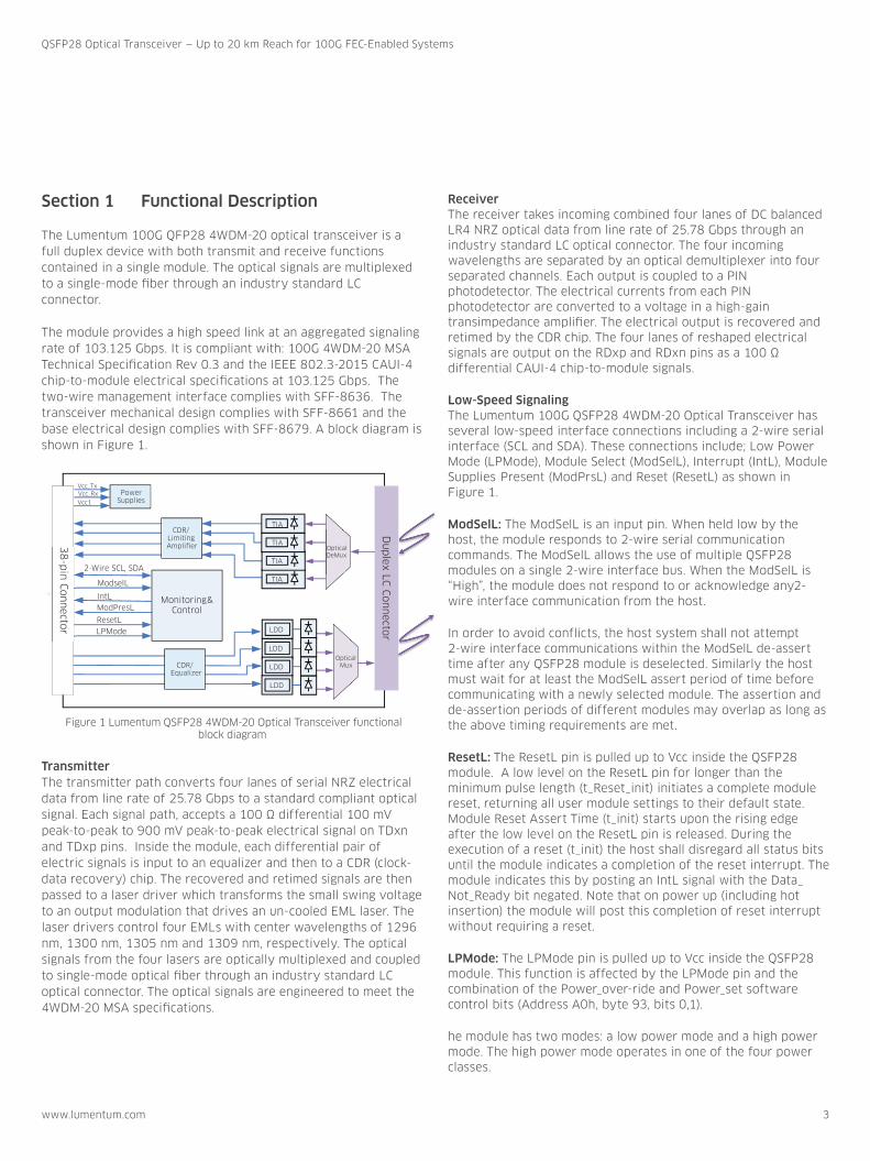
Application SchematicsAn example application schematic (reference SFF 8679) showing connections from a host IC and host power supply to the Lumentum 100G QSFP28 4WDM-20 optical transceiver is shown in Figure 2.
QSFP28 4WDM-20 modules are hot pluggable and active connections are powered by individual power connection at 3.3 V nominal voltage. Multiple modules can share a single 3.3 V power supply with individual filtering. To limit wide band noise power, the host system and module shall each meet a maximum of 2% peak-to-peak noise when measured with a 1 MHz low pass filter. In addition, the host system and the module shall each meet a maximum of 3% peak-to-peak noise when measured with a filter from 1 MHz - 10 MHz.
A module will meet all electrical requirements and remain fully operational in the presence of noise on the 3.3V power supply. Power supply filtering components should be placed as close to the V pins of the host connector as possible for optimal performance. Note: Decoupling Capacitor values vary depending on the application.
Tx Data Bus
Rx Data Bus
Micro Processor
Rx
Tx
QSFP28Module
ModPrsL
SDASCL
To other QSFP28 modulesVcc Host = +3.3V
LPModeResetL
IntLModSeIL
4.7k to 10k
VccRx
VccTx
HOST IC
Vcc1
Tx <1:4>
Rx <1:4>
Quad SERDES IC
Vcc Host = +3.3V
Figure 2. Typical application schematics for the Lumentum QSFP28 optical transceiver

QSFP28 Optical Transceiver — Up to 20 km Reach for 100G FEC-Enabled Systems
www.lumentum.com 5
Section 2 Specifications
Section 2.1 Pin Function Definitions
Section 2.2 QSFP28 4WDM-20 Lane Assignment
Section 2.3 Absolute Maximum Ratings
Section 2.4 Recommended Operating Condition
Section 2.5 Low Speed Electrical Characteristics
Section 2.6 Timing Requirement of Control and Status I/O
Section 2.7 Optical Transmitter Characteristics
Section 2.8 Optical Receiver Characteristics
Section 2.9 Link Power Budget Characteristics
Section 2.10 Electrical Input and Output Squelch Behavior
Section 2.11 Module CTLE Behavior
Section 2.12 Regulatory Compliance
Section 2.13 Module Outline
Section 2.14 Connectors
2.1 Pin Function Definitions
38 GND37 TX1n36 TX1p35 GND34 TX3n33 TX3p32 GND31 LPMode30 VCC129 VCCTx28 IntL27 ModPrsL26 GND25 RX4p24 RX4n23 GND22 RX2p21 RX2n20 GND
GND 1TX2n 2TX2p 3GND 4TX4n 5TX4p 6GND 7ModelL8ResetL 9VCCRx 10SCL 11SDA 12GND 13RX3p 14RX3n 15GND 16RX1p 17RX1n 18GND 19
Module C
ard E
dge
Top side Viewed from top
Bottom side Viewed from bottom
Figure 3 QSFP28 optical transceiver pin-out
QSFP28 Optical Transceiver — Up to 20 km Reach for 100G FEC-Enabled Systems
www.lumentum.com 6
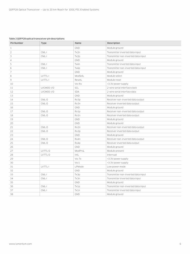
Table 2 QSFP28 optical transceiver pin descriptions
Pin Number Type Name Description
1 GND Module ground
2 CML-I Tx2n Transmitter inverted data input
3 CML-I Tx2p Transmitter non-inverted data input
4 GND Module ground
5 CML-I Tx4n Transmitter inverted data input
6 CML-I Tx4p Transmitter non-inverted data input
7 GND Module ground
8 LVTTL-I ModSelL Module select
9 LVTTL-I ResetL Module reset
10 Vcc Rx +3.3V power supply
11 LVCMOS-I/O SCL 2-wire serial interface clock
12 LVCMOS-I/O SDA 2-wire serial interface data
13 GND Module ground
14 CML-O Rx3p Receiver non-inverted data output
15 CML-O Rx3n Receiver inverted data output
16 GND Module ground
17 CML-O Rx1p Receiver non-inverted data output
18 CML-O Rx1n Receiver inverted data output
19 GND Module ground
20 GND Module ground
21 CML-O Rx2n Receiver non-inverted data output
22 CML-O Rx2p Receiver inverted data output
23 GND Module ground
24 CML-O Rx4n Receiver non-inverted data output
25 CML-O Rx4p Receiver inverted data output
26 GND Module ground
27 LVTTL-O ModPrsL Module present
28 LVTTL-O IntL Interrupt
29 Vcc Tx +3.3V power supply
30 Vcc1 +3.3V power supply
31 LVTTL-I LPMode Low power mode
32 GND Module ground
33 CML-I Tx3p Transmitter non-inverted data input
34 CML-I Tx3n Transmitter inverted data input
35 GND Module ground
36 CML-I Tx1p Transmitter non-inverted data input
37 CML-I Tx1n Transmitter inverted data input
38 GND Module ground
QSFP28 Optical Transceiver — Up to 20 km Reach for 100G FEC-Enabled Systems
www.lumentum.com 7
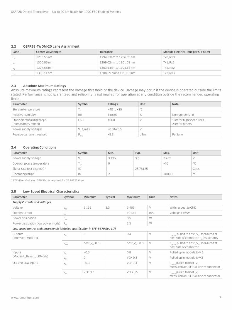
2.2 QSFP28 4WDM-20 Lane Assignment
Lane Center wavelength Tolerance Module electrical lane per SFF8679
L0 1295.56 nm 1294.53nm to 1296.59 nm Tx0, Rx0
L1 1300.05 nm 1299.02nm to 1301.09 nm Tx1, Rx1
L2 1304.58 nm 1303.54nm to 1305.63 nm Tx2, Rx2
L3 1309.14 nm 1308.09 nm to 1310.19 nm Tx3, Rx3
2.3 Absolute Maximum RatingsAbsolute maximum ratings represent the damage threshold of the device. Damage may occur if the device is operated outside the limits stated. Performance is not guaranteed and reliability is not implied for operation at any condition outside the recommended operating limits.
Parameter Symbol Ratings Unit Note
Storage temperature TST −40 to +85 °C
Relative humidity RH 5 to 85 % Non-condensing
Static electrical discharge(human body model)
ESD 1000 V 1 kV for high speed lines.2 kV for others
Power supply voltages VCC3, max −0.3 to 3.6 V
Receive damage threshold Pdmg +5.5 dBm Per lane
2.4 Operating Conditions
Parameter Symbol Min. Typ. Max. Unit
Power supply voltage Vcc 3.135 3.3 3.465 V
Operating case temperature TOP 0 +70 ºC
Signal rate (per channel) 1 fD 25.78125 Gbps
Operating range m 2 20000 m
1.FEC (Reed-Solomon 528,514) is required for 25.78125 Gbps
2.5 Low Speed Electrical Characteristics
Parameter Symbol Minimum Typical Maximum Unit Notes
Supply Currents and Voltages
Voltage VCC 3.135 3.3 3.465 V With respect to GND
Supply current Icc 1010.1 mA Voltage 3.465V
Power dissipation Pwr 3.5 W
Power dissipation (low power mode) Plp 1.5 W
Low speed control and sense signals (detailed specification in SFF-8679 Rev 1.7)
Outputs (Interrupt, ModPrsL)
VOL 0 0.4 V Rpullup pulled to host _Vcc, measured at host side of connector. IOL(max)=2mA
VOH host_Vcc-0.5 host_Vcc+ 0.3 V Rpullup pulled to host _Vcc, measured at host side of connector
Inputs (ModSelL, ResetL, LPMode)
VIL −0.3 0.8 V Pulled up in module to V 3
VIH 2 V 3+ 0.3 V Pulled up in module to V 3
SCL and SDA inputs VIL −0.3 V 3 * 0.3 V Rpullup pulled to host _V, measured at QSFP28 side of connector
VIH V 3 * 0.7 V 3 + 0.5 V Rpullup pulled to host _V, measured at QSFP28 side of connector

QSFP28 Optical Transceiver — Up to 20 km Reach for 100G FEC-Enabled Systems
www.lumentum.com 8
2.6 Timing Requirement of Control and Status I/O
Parameter Symbol Max Unit Notes
Initialization time t_init 60 s Time from power on, hot plug or rising edge of reset until the module is fully functional. This time does not apply to non-power level 0 modules in low-power state
Reset Init assert time t_reset_init 10 µs A Reset is generated by a low level longer than the minimum reset pulse time present on the ResetL pin
Serial bus hardware ready time t_serial 2000 ms Time from power on until the module responds to data transmission over the 2-wire serial bus
Monitor data ready time t_data 2000 ms Time from power on to data not ready, bit 0 of Byte 2, deasserted and IntL asserted
Reset assert time t_reset 60 s Time from rising edge on the ResetL pin until the module is fully functional
LPMode assert time ton_ LPMode 100 µs Time for assertion of LPMode (Vin: LPMode=Vin) until module power consumption reaches power level 1
LPMode deassert time Toff_ LPMode 300 ms Time for deassertion of LPMode (Vin:LPMode=Vil) until module is fully functional
IntL assert time ton_IntL 200 ms Time from occurrence of condition triggering IntL until Vout:IntL=Vol
IntL deassert time toff_IntL 500 µs Time from clear on read operation of associated flag until Vout:IntL=Voh. This includes deassert times for Rx Los, Tx Fault and other flag bits
Rx LOS assert time ton_los 100 ms Time from Rx LOS state to Rx LOS bit set (Value = 1b) and IntL asserted.
Tx Fault assert time ton_Txfault 200 ms Time from Tx Fault state to Tx Fault bit set (value = 1b) and IntL asserted
Flag assert time ton_flag 200 ms Time from occurrence of condition triggering flag to associated flag bit set (value=1b) and IntL asserted
Mask assert time ton_mask 100 ms Time from mask bit set (Value = 1b) until associated IntL assertion is inhibited
Mask deassert time toff_mask 100 ms Time from mask bit set (Value = 0b) until associated IntL operation resumes
Application or rate select change time t_ratesel 100 ms Time from change of state of Application or Rate Select bit until transmitter or receiver bandwidth is in conformance with appropriate specification, Not applicable
Power_over-ride or power-set assert time ton_Pdown 100 ms Time from P_Down bit set (Value = 1b) until module power consumption reaches Power Level 1
Power_over-ride or power-set deassert time toff_Pdown 300 ms Time from P_Down bit set (Value = 0b) until module is fully functional

QSFP28 Optical Transceiver — Up to 20 km Reach for 100G FEC-Enabled Systems
www.lumentum.com 9
2.7 Optical Transmitter Characteristics
Parameter Symbol Min Max Unit Notes
Signaling rate, each lane 25.78125 ± 100 ppm GBd
The following specifications are applicable within the operating case temperature range
Line wavelengths
1294.53 to 1296.59 1299.02 to 1301.09 1303.54 to 1305.63 1308.09 to 1310.19
nm
Optical modulation amplitude, each lane 1 OMA -1.3 4.5 dBm
Transmitter and dispersion penalty, each lane 2 TDP 2.8 dB
OMA minus TDP, each lane OMA-TDP -2.3 dBm
Average launch power, each lane 3,4 Pavg -4.3 4.5 dBm
Total launch power Pavg_total 10.5 dBm
Extinction ratio ER 4.0 dB
Side-mode suppression ratio SMSR 30 dB
Difference in launch power between any two lanes (OMA) 5.0 dB
Average launch power of OFF transmitter, each lane Toff -30 dBm
Optical return loss tolerance ORL 20 dB
Transmitter reflectance 5 -26 dB
Transmitter eye mask {X1, X2, X3, Y1, Y2, Y3} { 0.25, 0.4, 0.45, 0.25, 0.28, 0.4} Eye mask hit ratio is 5E-5
Tx DD reporting accuracy4 TxDD Error -2 +2 dB
1.Even if the TDP < 1.0dB, the OMA (min) must exceed this value.
2.TDP does not include a penalty for multi-path interference (MPI).
3.Average launch power, each lane (min) is informative and not the principal indicator of signal strength. A transmitter with launch power below this value cannot be compliant; however, a value above this does not ensure compliance.
4.Measured using an external wavelength demultiplexer with all four channels enabled.
5.Transmitter reflectance is defined looking into the transmitter.

QSFP28 Optical Transceiver — Up to 20 km Reach for 100G FEC-Enabled Systems
www.lumentum.com 10
2.8 Optical Receiver Characteristics
Parameter Symbol Min Max Unit Notes
Signaling rate, each lane 25.78125 ± 100 ppm GBd
The following specifications are applicable within the operating case temperature range
Line Wavelengths 1 1294.53 to 1296.59 1299.02 to 1301.09 1303.54 to 1305.63 1308.09 to 1310.19
nm
Damage threshold 1 5.5 dBm
Average receive power, each lane 2 Pavg -14.5 4.5 dBm
Receiver reflectance -26 dB
Receiver Sensitivity (OMA), each lane 3 Rx Sens -12.5 dBm 5E-5 BER, pre-FEC, PRBS31, using typical LUMENTUM transmitter
Stressed receiver sensitivity (OMA), each lane 4 SRS -10.0 dBm Measured with conformance test signal at TP3 for BER = 5E-5.
Stressed receiver sensitivity test conditions [ Note: test conditions for measuring stress receiver sensitivity, not characteristic of the receiver]
Vertical eye closure penalty, each lane VECP 2.5 dB
Stressed sys J2 jitter, each lane J2 0.33 UI
Stressed sys J4 jitter, each lane J4 0.48 UI
SRS eye mask definition {X1, X2, X3, Y1, Y2, Y3} {0.39, 0.5, 0.5, 0.39, 0.39, 0.4}
LOS assert LOS_A -15 dBm
LOS hysteresis LOS_Hys 0.5 dB
RxDD reporting accuracy RxDD Error -2 +2 dB
1.The receiver shall be able to tolerate, without damage, continuous exposure to an optical signal having this average power level
2.Average receive power, each lane (min) is informative and not the principal indicator of signal strength. A received power below this value cannot be compliant; however, a value above this does not ensure compliance.
3.Receiver sensitivity (OMA),each lane (max) at 5E-5 BER is an normative specification4. Refer to IEEE Std 802.3-2015 CI.88.8.10
4.Measured with conformance test signal at TP3 (see 4WDM-20 MSA sec 3.10) for BER = 5E-5
2.9 Link Power Budget Characteristics
Parameter Value Unit Notes
Power Budget ( for max TDP) 13 dB
Operating Distance 20 km
Maximum Discrete Reflectance -26 dB
Channel Insertion Loss 1 0 to 10.2 dB
Allocation for penalties (for max TDP) 2.8 dB
Additional Insertion Loss Allowed 0 dB
1.The channel insertion loss budget may include up to 0.2 dB MPI loss penalty to support worst case transmitter/receiver with worst case connector.
2.10 Electrical Input and Output Squelch BehaviorThe Lumentum 100G QSFP28 Optical Transceiver is compliant to the Tx and Rx squelch behavior described in SFF-8636 section 6.6.2 and will be indicated in Page 00h, Byte 194, bit 0:3.
Rx(n)(p/n) are QSFP28 module receiver data outputs. Output squelch for loss of optical input signal, hereafter Rx Squelch, is supported by the Lumentum QSFP28 transceiver. In the event of the optical signal on any channel becoming equal to or less than the level required to assert LOS, then the receiver data output for that channel shall be squelched or disabled. In the squelched or disabled state output impedance levels are maintained while the differential voltage swing shall be less than 50 mVpp.
In normal operation the default case has Rx Squelch active. Rx Squelch can be deactivated using Rx Squelch Disable through the 2-wire serial interface. For the Lumentum 100G QSFP28 Optical Transceiver, squelch and output disable is controlled for each channel using bytes 240 and 241 of page 03h. Writing a '1' in the Squelch Disable register (byte 240, page 03h) disables the squelch for the
QSFP28 Optical Transceiver — Up to 20 km Reach for 100G FEC-Enabled Systems
www.lumentum.com 11
Table 3 Regulatory Compliance
Feature Test Method Performance
Safety
Product safety UL 60950-1 UL recognized component for US and CAN
CSA C22.2 No. 60950-1
EN 60950-1 TUV certificate
IEC 60950-1 CB certificate
Flame class V-0 Passes Needle Flame Test for component flammability verification
Low Voltage Directive 2014/35/EU Certified to harmonized standards listed; Declaration of Conformity issued
Laser safety EN 60825-1, EN 60825-2 TUV certificate
IEC 60825-1 CB certificate
U.S. 21 CFR 1040.10 FDA/CDRH certified with accession number
Electromagnetic compatibility
Radiated emissions EMC Directive 2014/30/EU Class B digital device with a minimum -6dB margin to the limit. Final margin may vary depending on system implementation. Tested frequency range: 30 MHz to 40 GHz or 5th harmonic (5 times the highest frequency), whichever is less.Good system EMI design practice is required to achieve Class B margins at the system level.
FCC rules 47 CFR Part 15
CISPR22, CISPR32
AS/NZS CISPR22, CISPR32
EN 55022, EN 55032
ICES-003, Issue 6
VCCI regulations
Immunity EMC Directive 2014/30/EU Certified to harmonized standards listed; Declaration of Conformity issuedCISPR24
EN 55024
ESD IEC/EN 61000-4-2 Exceeds Requirements. Withstands discharges of ±8kV contact, ±15kV air
Radiated immunity IEC/EN 61000-4-3 Exceeds Requirements. Field strength of 10V/m from 80 MHz to 6 GHz. No effect on transmitter / receiver performance is detectable between these limits.
Restriction of hazardous substances (ROHS)
RoHS EU Directive 2011/65/EU Compliant per the Directive 2011/65/EU of the European Parliament and of the Council of 8 June 2011 on the restriction of the use of certain hazardous substances in electrical and electronic equipment (recast).
associated channel. Writing a '1' in the Output Disable register (byte 241, page 03h) squelches the output of the associated channel. When a '1' is written in both registers for a channel, the associated output is disabled.
The Lumentum 100G QSFP28 Optical Transceiver will disable Tx Squelch Function as default. Tx(n)(p/n) are QSFP28 module transmitter data inputs and Tx Squelch is implemented to reduce OMA only (Page 00h, Byte 195, bit 2=0b). For details regarding Tx Squelch behaviors, please contact Lumentum to learn more.
2.11 Module CTLE BehaviorThe Lumentum 100G QSFP28 Optical Transceiver supports manual (provisional) equalization with non-readable CTLE gain. Please contact Lumentum for details if automatic (adaptive) equalization is preferred.
2.12 Regulatory ComplianceThe Lumentum 100G QSFP28 Optical Transceiver is RoHS 6/6 compliant and complies with international EMC (Electromagnetic Compatibility) and product safety requirements and standards.
QSFP28 Optical Transceiver — Up to 20 km Reach for 100G FEC-Enabled Systems
www.lumentum.com 12
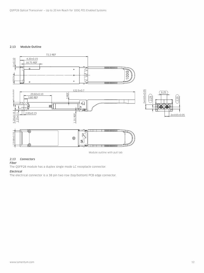
2.13 Module Outline
72.2 REF
4.20±0.15
16.75 REF
1±
0.1
0
18
.35
±0
.10
2x6
±0
.2
29.60±0.103.80 REF
1.7
0±
0.1
0
8.5
0±
0.1
0
5.2
0±
0.1
5
2.2
5±
0.1 2.00±0.15
122.5±0.7
3 R
EF
1.3
1 R
EF
16
.42
±0
.08
13
.68
±0
.10
2x4
.65
±0
.05
2x4.65±0.05
6.25
2.2
9
2.2
9
2.13 Connectors FiberThe QSFP28 module has a duplex single mode LC receptacle connector.
ElectricalThe electrical connector is a 38 pin two row (top/bottom) PCB edge connector.
Module outline with pull tab
QSFP28 Optical Transceiver — Up to 20 km Reach for 100G FEC-Enabled Systems
www.lumentum.com 13
Section 3 Related Information
Section 3.1 Packing and Handling Instructions
Section 3.2 Electrostatic Discharge (ESD)
Section 3.3 Laser Safety
Section 3.4 EMC Compliance
3.1 Package and Handling Instructions
Connector CoversThe Lumentum 100G QSFP28 Optical Transceiver is supplied with an LC duplex receptacle. The connector plug supplied protects the connector during standard manufacturing processes and handling by preventing contamination from dust, aqueous solutions, body oils, or airborne particles.
Note: It is recommended that the connector plug remain on whenever the transceiver optical fiber connector is not inserted.
Recommended Cleaning and De-Greasing Chemicals LUMENTUM recommends the use of methyl, isopropyl and isobutyl alcohols for cleaning.
Do not use halogenated hydrocarbons (e.g. trichloroethane, ketones such as acetone, chloroform, ethyl acetate, MEK, methylene chloride, methylene dichloride, phenol, N-methylpyrolldone).
This product is not designed for aqueous wash.
Housing The Lumentum QSFP28 Optical Transceiver housing is made from zinc.
3.2 Electrostatic Discharge (ESD)
HandlingNormal ESD precautions are required during the handling of this module. This transceiver is shipped in ESD protective packaging. It should be removed from the packaging and otherwise handled only in an ESD protected environment utilizing standard grounded benches, floor mats, and wrist straps.
Test and OperationIn most applications, the optical connector will protrude through the system chassis and be subjected to the same ESD environment as the system. Once properly installed in the system, this transceiver should meet and exceed common ESD testing practices and fulfill system ESD requirements.
Typical of optical transceivers, this module’s receiver contains a highly sensitive optical detector and amplifier which may become temporarily saturated during an ESD strike. This could result in a short burst of bit errors. Such an event might require that the application re-acquire synchronization at the higher layers (e.g. Serializer / Deserializer chip).
3.3 Laser SafetyThe transceiver is certified as a Class 1 laser product per international standard IEC 60825-1:2014 3rd edition and is considered non-hazardous when operated within the limits of this specification. This device complies with 21 CFR 1040.10 except for deviations pursuant to Laser Notice No.50.
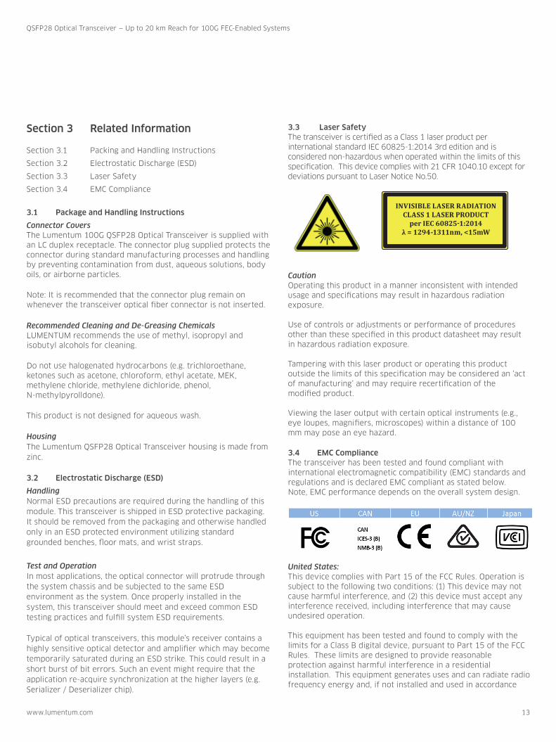
INVISIBLE LASER RADIATIONCLASS 1 LASER PRODUCT
per IEC 60825-1:2014λ = 1294-1311nm, <15mW
CautionOperating this product in a manner inconsistent with intended usage and specifications may result in hazardous radiation exposure.
Use of controls or adjustments or performance of procedures other than these specified in this product datasheet may result in hazardous radiation exposure.
Tampering with this laser product or operating this product outside the limits of this specification may be considered an ‘act of manufacturing’ and may require recertification of the modified product.
Viewing the laser output with certain optical instruments (e.g., eye loupes, magnifiers, microscopes) within a distance of 100 mm may pose an eye hazard.
3.4 EMC Compliance The transceiver has been tested and found compliant with international electromagnetic compatibility (EMC) standards and regulations and is declared EMC compliant as stated below. Note, EMC performance depends on the overall system design.
United States:This device complies with Part 15 of the FCC Rules. Operation is subject to the following two conditions: (1) This device may not cause harmful interference, and (2) this device must accept any interference received, including interference that may cause undesired operation.
This equipment has been tested and found to comply with the limits for a Class B digital device, pursuant to Part 15 of the FCC Rules. These limits are designed to provide reasonable protection against harmful interference in a residential installation. This equipment generates uses and can radiate radio frequency energy and, if not installed and used in accordance

North AmericaToll Free: 844 810 LITE (5483)
Outside North AmericaToll Free: 800 000 LITE (5483)
ChinaToll Free: 400 120 LITE (5483)
© 2017 Lumentum Operations LLCProduct specifications and descriptions in this document are subject to change without notice.
qsfp28-4wdm-20-ds-oc-ae 30179561 003 1017
QSFP28 Optical Transceiver — Up to 20 km Reach for 100G FEC-Enabled Systems
Lumentum Operations LLC 400 North McCarthy Boulevard Milpitas, CA 95035 USA www.lumentum.com
Japan:
Translation: This is a Class B product based on the standard of the Voluntary Control Council for Interference from Information Technology Equipment (VCCI). If this is used near a radio or television receiver in a domestic environment, it may cause radio interference. Install and use the equipment according to the instruction manual.
Ordering InformationFor more information on this or other products and their availability, please contact your local Lumentum account manager or Lumentum directly at 1-800-498-LUMENTUM (1-800-498- 5378) in North America and +800-5378-LUMENTUM (+800-5378-5378) worldwide or via e-mail at customer.service@ Lumentum.com.
Description Product Code
100GE, 20 km reach, 4WDM-20, commercial temperature range, QSFP28 optical transceiver, pull tab
LQ210LR-CAP3
with the instructions, may cause harmful interference to radio communications. However, there is no guarantee that interference will not occur in a particular installation. If this equipment does cause harmful interference to radio or television reception, which can be determined by turning the equipment off and on, the user is encouraged to try to correct the interference by one or more of the following measures:
• Reorient or relocate the receiving antenna.
• Increase the separation between the equipment and receiver.
• Connect the equipment into an outlet on a circuit different from that to which the receiver is connected.
• Consult the dealer or an experienced radio/TV technician for help.
Caution: Any changes or modifications to the product not expressly approved by the Lumentum Operations LLC could void the user's authority to operate this equipment.
Canada: ICES-3 (B) / NMB-3 (B)
This Class B digital apparatus complies with Canadian ICES-003.
Cet appareil numérique de la classe B est conforme à la norme NMB-003 du Canada.
European Union:This product complies with the European Union’s Low Voltage Directive 2014/35/EU and EMC Directive 2014/30/EU and is properly CE marked. This declaration is made by Lumentum Operations LLC which is solely responsible for the declared compliance.