Embed Size (px)
Citation preview
Q48SC12050 600W DC/DC Power Modules
DS_Q48SC12050_07112017 E-mail: [email protected]
http://www.deltaww.com/dcdc
P1
FEATURES
Input voltage range: 36V~75V
Output voltage range ( trim and PMBUS)
8V~13.2V
Fully regulated from 36 to 75Vin
High efficiency : 94.2% @ 48Vin/50A
95.6% @ 48Vin/30A
Size:
58.4mm x 36.8mm x 12.7mm (2.3” x 1.45” x 0.50”)
Industry standard DOSA compliant pin out
Fully protected: Input UVLO, Output OCP and
OVP, OTP
Droop current sharing
1500V isolation
No minimum load required
Fixed frequency operation
ISO 9001, TL 9000, ISO 14001, QS9000,
OHSAS18001 certified manufacturing facility
UL/CUL 60950-1 (US & Canada)
Delphi Series Q48SC12050, Quarter Brick Family
DC/DC Power Modules: 36~75Vin, 12Vout, 600W
The Delphi series Q48SC12050, quarter brick, 36~75V input,
single output 12V, are full digital control DC/DC converter, and
are the latest offering from a world leader in power system and
technology and manufacturing ― Delta Electronics, Inc. This
product provides up to 600 watts of power at 36~75V input in an
industry standard, DOSA compliant footprint and pin out. The
Q48SC12050 offers more than 94.2% high efficiency at 48V
input, 12V output and 50A load. There is a built-in digital PWM
controller in the Q48SC12050 series, which is used to complete
the Vo feedback, PWM signal generation, droop current sharing,
fault protection, output voltage trim, on/off control and PMBUS
communications, and so on. With the digital control, many
design and application flexibility, advanced performance, and
reliability are obtained. The Q48SC12050 can be connected in
parallel directly for higher power without adding external
oring-fet.
OPTIONS
Positive or Negative On/Off logic
Droop current sharing
Digital pins
APPLICATIONS
Datacom / Networking
Wireless networks
Optical network equipment
Server and data storage
Industrial / Test equipment
DS_Q48SC12050_07112017 E-mail: [email protected]
http://www.deltaww.com/dcdc P2
TECHNICAL SPECIFICATIONS (TA=25°C, airflow rate=400 LFM, Vin=48Vdc, nominal Vout unless otherwise noted.)
PARAMETER NOTES and CONDITIONS Q48SC12050 Min. Typ. Max. Units
ABSOLUTE MAXIMUM RATINGS
Input Voltage
Continuous 0 75 Vdc
Transient (100ms) 100ms 100 Vdc
On/off Pin Voltage -50 50 V
Other Pin Voltage Trim/Current Sharing, C2, Data, SMBAlert, Clock, Addr1,
Addr0 -0.3 3.6 V
Output negative voltage 0.3 V
Operating ambient Temperature -40 85 °C
Storage Temperature -55 125 °C
Input/Output Isolation Voltage 1500 Vdc INPUT CHARACTERISTICS
Operating Input Voltage 36 48 75 Vdc
Input Under-Voltage Lockout
Turn-On Voltage Threshold
(Adjustable via PMBus, VIN_ON) 34 36 Vdc
Turn-Off Voltage Threshold (Adjustable via PMBus, VIN_OFF)
31 34 Vdc
Lockout Hysteresis Voltage 2 Vdc
Maximum Input Current Vin=36V, 100% Load 19 A
No-Load Input Current Vin=48V 80 110 140 mA
Off Converter Input Current Vin=48V 10 18 26 mA
Input Capacitance 100 uF
Inrush Current (I2t) 1 A2S
Input Reflected-Ripple Current P-P thru 12µH inductor, 5Hz to 20MHz 60 mA
Input Voltage Ripple Rejection 120Hz 50 dB OUTPUT CHARACTERISTICS
The module without droop current sharing option code
Output Voltage Set Point (Adjustable via PMBus)
Vin=48V, Io=0A , Ta=25°C 11.88 12 12.12 Vdc
Output Voltage Regulation
Over Line Vin=36V to 75V, Io=100% load ±40 mV
Over Load Vin=36V to 75V, Io=Io,min to Io,max ±40 mV
Over tempearture Vin=36V to 75V, Io=100% load, Ta= -40C to 85C ±120 mV
The module with droop current sharing option code
Output Voltage Set Point (Adjustable via PMBus)
Vin=48V, Io=0A , Ta=25°C 12.28 12.4 12.52 Vdc
Output Voltage Regulation
Over Line Vin=36V to 75V, Io=100% load ±40 mV
Over Load Vin=36V to 75V, Io=Io,min to Io,max -850 -680 mV
Over tempearture Vin=36V to 75V, Io=100% load, Ta= -40C to 85C ±80 mV
Both with and without droop current sharing option code
Output Voltage Trim and PMBUS Range Vin=36V to 75V, Pout ≦ max rated power,Io ≦ Io.max -33.3 +10 %
Output Voltage Remote Sense Range (note 2) Vin=36V to 75V, Pout ≦ max rated power,Io ≦ Io.max -5.8 +10 %
Output Over-Voltage Lockout (Adjustable via PMBus, VOUT_OV_FAULT_LIMIT)
15.2 Vdc
Operating Output Current Range Full input voltage range 0 50 A
Output DC Current-Limit Inception 115 135 %
Output Capacitance 300 15000 µF
Output Voltage Ripple and Noise Vin=48V, Full load, 20MHz bandwidth
Peak-to-Peak Co= 300uF/16V (polymer ) + 10u/16V (Tantalum Capacitor)
+1u/16V (Ceramic ) 75 110 mV
RMS Co= 300uF/16V (polymer ) + 10u/16V (Tantalum Capacitor)
+1u/16V (Ceramic ) 22 32 mV
DYNAMIC CHARACTERISTICS
Output Voltage Current Transient Vin=48V, Load Slew rate 0.1A/µs with a 1uF ceramic ,
a 10uF tantalum, and a 300uF polymer capacitor
Positive Step Change in Output Current 50% Io.max to 75% Io.max 350 500 mV
Negative Step Change in Output Current 75% Io.max to 50% Io.max -500 -350 mV
Settling Time (within 1% Vout nominal) 500 µs
Turn-On Transient (Adjustable via PMBus)
Start-Up Time, From On/Off Control From On/off to 90%Vo final value 55 ms
Start-Up Time, From Input From Input to 90%Vo final value 75 ms
Output voltage Rise Time From 10%Vo final value to 90%Vo final value 30 ms EFFICIENCY
100% Load Vin=48V 94.2 %
60% Load Vin=48V 95.6 % ISOLATION CHARACTERISTICS
Input to Output 1500 Vdc
Isolation Resistance 10 MΩ
Isolation Capacitance 6800 pF
DS_Q48SC12050_07112017 E-mail: [email protected]
http://www.deltaww.com/dcdc P3
TECHNICAL SPECIFICATIONS (TA=25°C, airflow rate=400 LFM, Vin=48Vdc, nominal Vout unless otherwise noted.)
DIGITAL INTERFACE SPECIFICATIONS (TA=25°C, airflow rate=400 LFM, Vin=48Vdc, nominal Vout unless otherwise noted.)
PIN DEFINATION
Pin# Name Function Pin# Name Function
1 VIN(+) 9 VOUT(+)
2 ON/OFF Primary on/off control pin
10 C2 PGOOD pin, and this pin also could be configurated as secondary on/off control pin
3 Case 11 SIG_GND Signal ground
4 VIN(-) 12 DATA PMBus data line
5 VOUT(-) 13 SMBALERT PMBus SMBAlert line
6 SENSE(-) Remote sense 14 CLOCK PMBus clock line
7 TRIM Trim note 3
15 ADDR1 ADDR1 pin sets the high order digit of the address.
8 SENSE(+) Remote sense 16 ADDR0 ADDR0 pin sets the low order digit of the address.
Note3: see the last page.
PARAMETER NOTES and CONDITIONS Q48SC12050 Min. Typ. Max. Units
FEATURE CHARACTERISTICS
Switching Frequency 130 KHz
ON/OFF Control, Remote On/Off logic Default Negative logic
Logic Low (Module On) Von/off at Ion/off=1.0mA -0.7 0.8 V
Logic High (Module Off) Von/off at Ion/off=0.0 µA 3.5 50 V
ON/OFF Current (for both remote on/off logic) Ion/off at Von/off=0.0V 0.5 mA
GENERAL SPECIFICATIONS
MTBF Io=80% of Io max; Ta=25°C; Airflow=600LFM 2.4 M
Weight 65 grams
Over-Temperature Shutdown (With heat spreader) Refer to Figure 22 for Hot spot's location
(48Vin,80% Io, 200LFM,Airflow from Vin+ to Vin-) 110 °C
Over-Temperature Shutdown ( NTC resistor ) 125 °C
Note1: Please attach thermocouple on NTC resistor to test OTP function, the hot spots’ temperature is just for reference. And the OTP is Adjustable via PMBus. Note2: Output voltage range 5.8% for remote sense-; Output voltage range 10% for remote sense+.
PARAMETER NOTES and CONDITIONS Q48SC12050
Min. Typ. Max. Units
PMBUS SIGNAL INTERFACE CHARACTERISTICS
Input High Voltage (CLK, DATA) 2.1 3.3 Vdc
Input Low Voltage (CLK, DATA) 0 0.8 Vdc
Input high level current (CLK, DATA) -10 10 uA
Input low level current (CLK, DATA) -10 10 uA
Output Low Voltage (SMBALERT#) SMBALERT, sink current 2mA 0.4 Vdc
Output high level open drain leakage current (SMBALERT#)
SMBALERT, 3.6V 0 10 uA
PMBus Operating frequency range 100 or 400 kHz
Measurement System Characteristics
Output current reading accuracy 10.5A<IOUT<50A -5 1.4 3 %
1A<IOUT<10.5A -1.7 2.5 A
VOUT reading accuracy 1 %
VIN reading accuracy -2 +2 Vdc
Temperature sense range 0 °C
Temperature reading accuracy Temperature>0°C -5 +5 °C
DS_Q48SC12050_07112017 E-mail: [email protected]
http://www.deltaww.com/dcdc P4
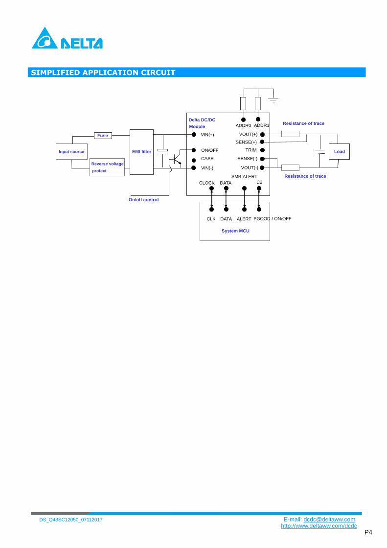
SIMPLIFIED APPLICATION CIRCUIT
VOUT(+)
TRIM
ADDR0 ADDR1
ON/OFF
Delta DC/DC Module
EMI filter
Fuse
Load Input source
System MCU
CLOCK DATA C2 SMB-ALERT
CLK DATA PGOOD / ON/OFF ALERT
On/off control
VIN(-)
SENSE(-)
SENSE(+)
VOUT(-)
VIN(+)
Reverse voltage
protect
Resistance of trace
Resistance of trace
CASE
DS_Q48SC12050_07112017 E-mail: [email protected]
http://www.deltaww.com/dcdc P5
ELECTRICAL CHARACTERISTICS CURVES
74
76
78
80
82
84
86
88
90
92
94
96
98
2 6 10 14 18 22 26 30 34 38 42 46 50
OUTPUT CURRENT (A)
EF
FIC
IEN
CY
(%)
36V 75V48V
2
6
10
14
18
22
26
30
34
38
42
2 6 10 14 18 22 26 30 34 38 42 46 50
OUTPUT CURRENT(A)P
OW
ER
DIS
SIP
AT
ION
(W
)
36V
48V
75V
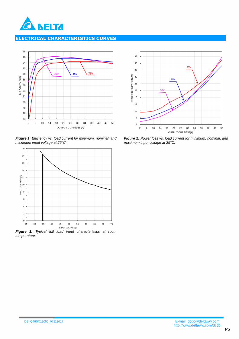
Figure 1: Efficiency vs. load current for minimum, nominal, and maximum input voltage at 25°C.
Figure 2: Power loss vs. load current for minimum, nominal, and maximum input voltage at 25°C.
0
2
4
6
8
10
12
14
16
18
20
25 30 35 40 45 50 55 60 65 70 75
INPUT VOLTAGE(V)
INP
UT
CU
RR
EN
T(A
)
Figure 3: Typical full load input characteristics at room temperature.
DS_Q48SC12050_07112017 E-mail: [email protected]
http://www.deltaww.com/dcdc P6
ELECTRICAL CHARACTERISTICS CURVES
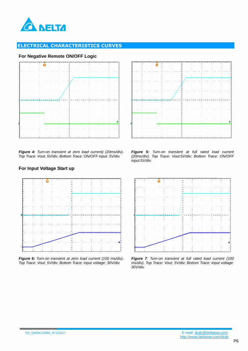
For Negative Remote ON/OFF Logic
Figure 4: Turn-on transient at zero load current) (20ms/div). Top Trace: Vout; 5V/div; Bottom Trace: ON/OFF input: 5V/div.
Figure 5: Turn-on transient at full rated load current (20ms/div). Top Trace: Vout:5V/div; Bottom Trace: ON/OFF input:5V/div.
For Input Voltage Start up
Figure 6: Turn-on transient at zero load current (100 ms/div). Top Trace: Vout; 5V/div; Bottom Trace: input voltage: 30V/div.
Figure 7: Turn-on transient at full rated load current (100 ms/div). Top Trace: Vout; 5V/div; Bottom Trace: input voltage: 30V/div.
DS_Q48SC12050_07112017 E-mail: [email protected]
http://www.deltaww.com/dcdc P7
ELECTRICAL CHARACTERISTICS CURVES
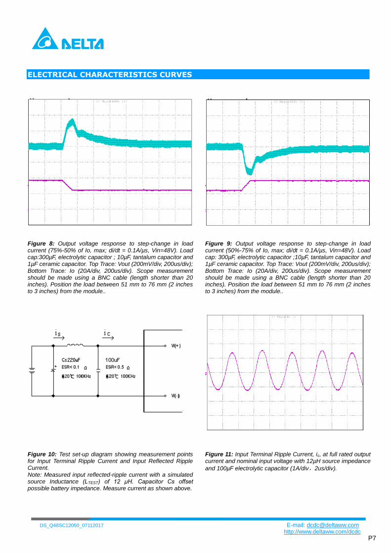
Figure 8: Output voltage response to step-change in load current (75%-50% of Io, max; di/dt = 0.1A/µs, Vin=48V). Load cap:300µF, electrolytic capacitor ; 10µF, tantalum capacitor and 1µF ceramic capacitor. Top Trace: Vout (200mV/div, 200us/div); Bottom Trace: Io (20A/div, 200us/div). Scope measurement should be made using a BNC cable (length shorter than 20 inches). Position the load between 51 mm to 76 mm (2 inches to 3 inches) from the module..
Figure 9: Output voltage response to step-change in load current (50%-75% of Io, max; di/dt = 0.1A/µs, Vin=48V). Load cap: 300µF, electrolytic capacitor ;10µF, tantalum capacitor and 1µF ceramic capacitor. Top Trace: Vout (200mV/div, 200us/div); Bottom Trace: Io (20A/div, 200us/div). Scope measurement should be made using a BNC cable (length shorter than 20 inches). Position the load between 51 mm to 76 mm (2 inches to 3 inches) from the module..
Figure 10: Test set-up diagram showing measurement points for Input Terminal Ripple Current and Input Reflected Ripple Current. Note: Measured input reflected-ripple current with a simulated source Inductance (LTEST) of 12 μH. Capacitor Cs offset possible battery impedance. Measure current as shown above.
Figure 11: Input Terminal Ripple Current, ic, at full rated output current and nominal input voltage with 12µH source impedance
and 100µF electrolytic capacitor (1A/div,2us/div).
DS_Q48SC12050_07112017 E-mail: [email protected]
http://www.deltaww.com/dcdc P8
ELECTRICAL CHARACTERISTICS CURVES
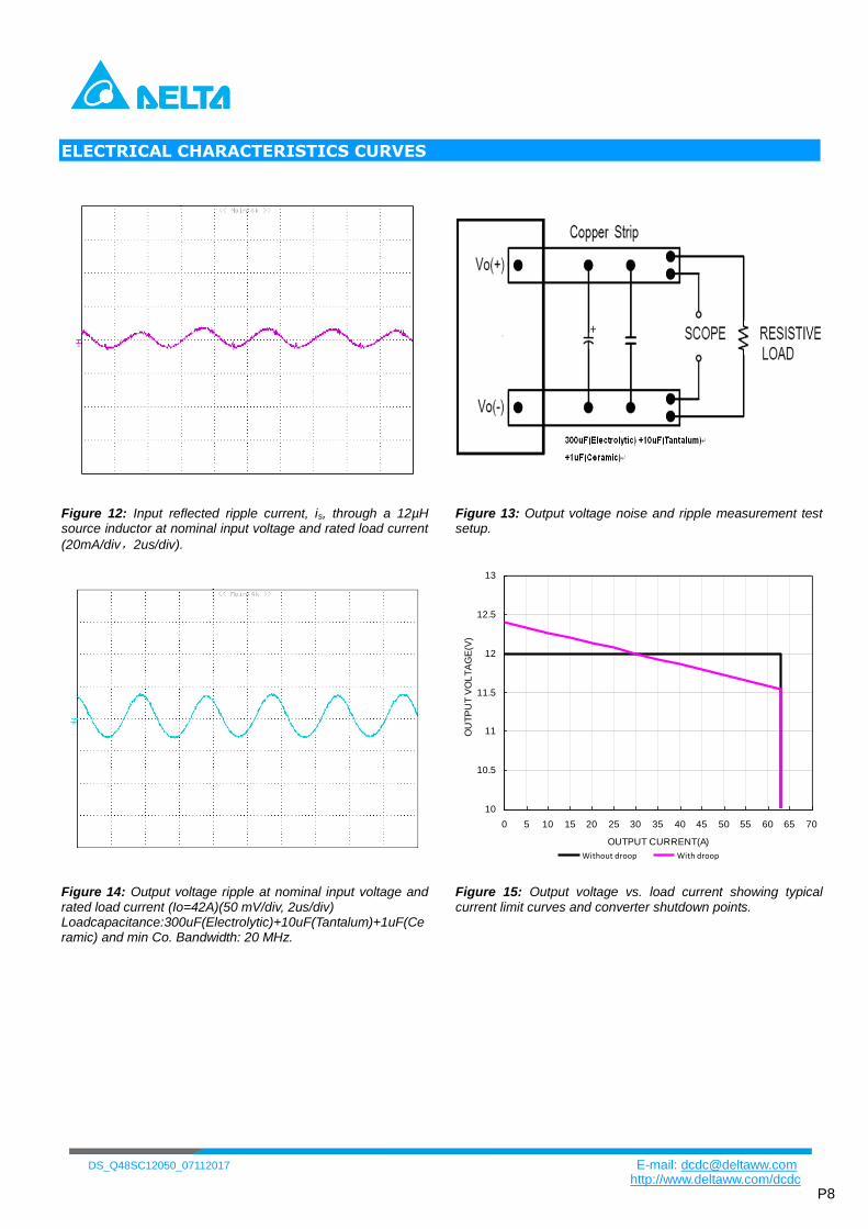
Figure 12: Input reflected ripple current, is, through a 12µH source inductor at nominal input voltage and rated load current
(20mA/div,2us/div).
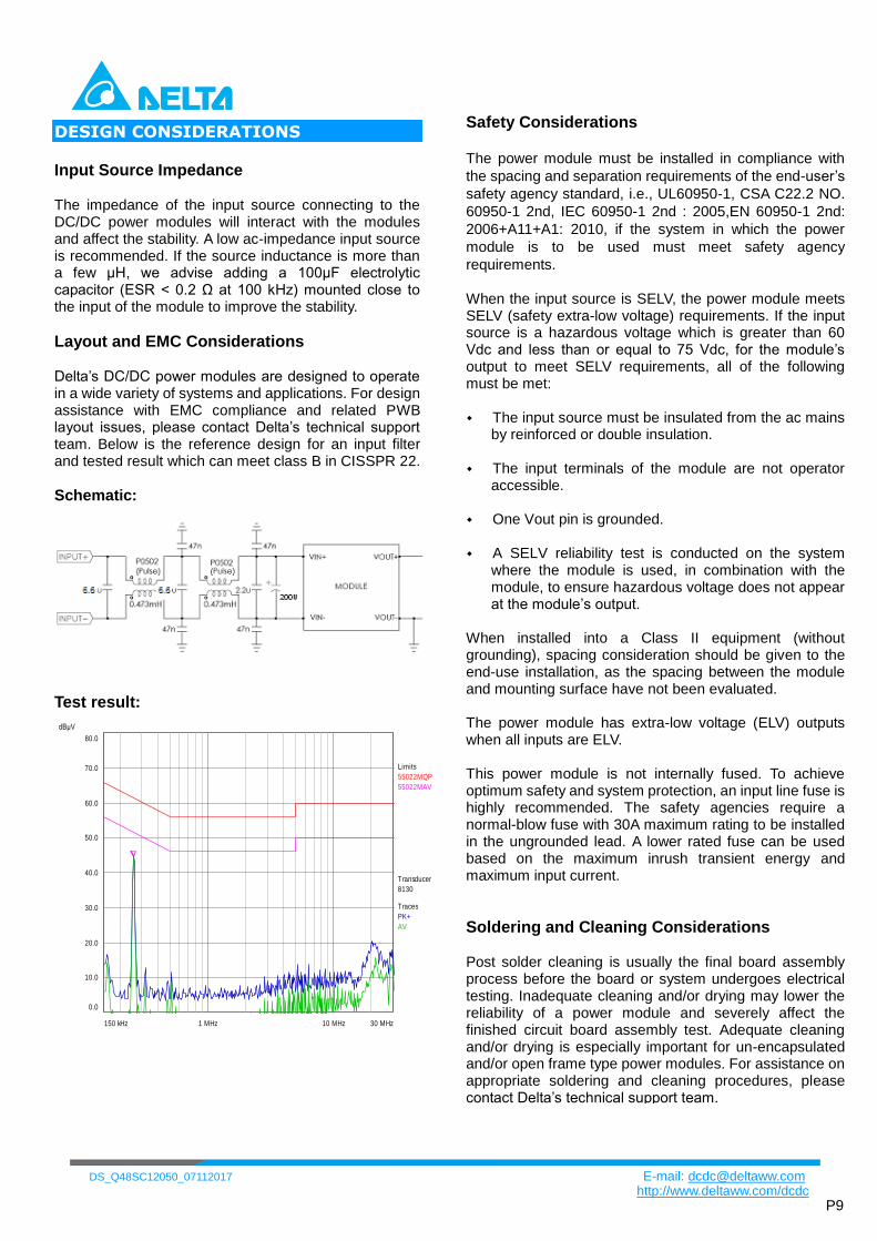
Figure 13: Output voltage noise and ripple measurement test setup.
10
10.5
11
11.5
12
12.5
13
0 5 10 15 20 25 30 35 40 45 50 55 60 65 70
OUTPUT CURRENT(A)
OU
TP
UT
VO
LT
AG
E(V
)
Without droop With droop
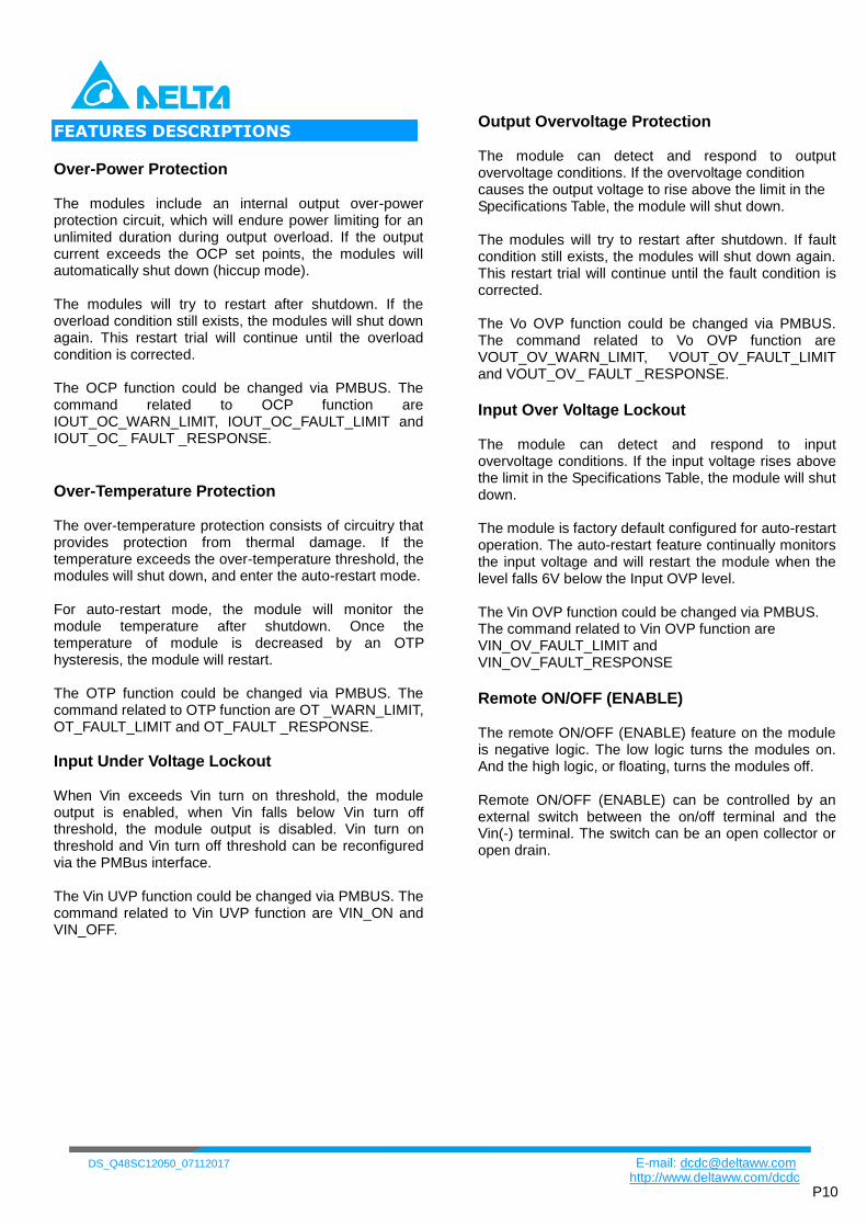
Figure 14: Output voltage ripple at nominal input voltage and rated load current (Io=42A)(50 mV/div, 2us/div) Loadcapacitance:300uF(Electrolytic)+10uF(Tantalum)+1uF(Ceramic) and min Co. Bandwidth: 20 MHz.
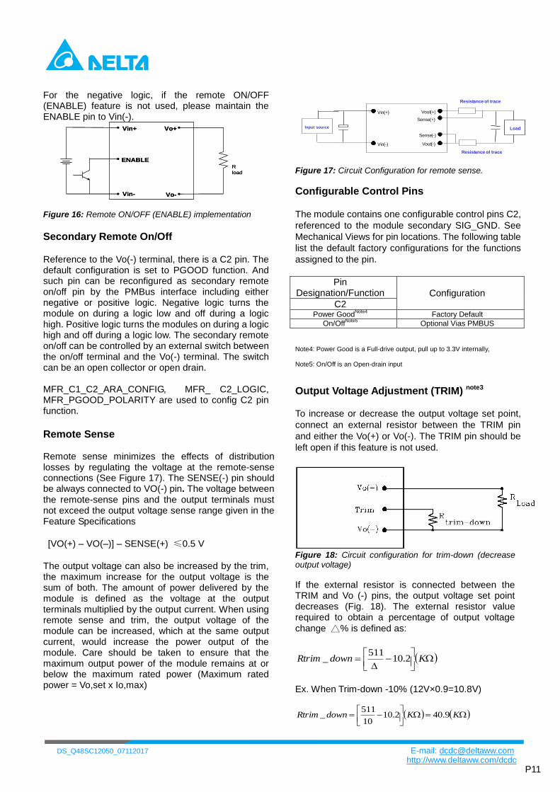
Figure 15: Output voltage vs. load current showing typical current limit curves and converter shutdown points.
DS_Q48SC12050_07112017 E-mail: [email protected]
http://www.deltaww.com/dcdc P9
DESIGN CONSIDERATIONS
Input Source Impedance
The impedance of the input source connecting to the DC/DC power modules will interact with the modules and affect the stability. A low ac-impedance input source is recommended. If the source inductance is more than a few μH, we advise adding a 100μF electrolytic capacitor (ESR < 0.2 Ω at 100 kHz) mounted close to the input of the module to improve the stability.
Layout and EMC Considerations
Delta’s DC/DC power modules are designed to operate in a wide variety of systems and applications. For design assistance with EMC compliance and related PWB layout issues, please contact Delta’s technical support team. Below is the reference design for an input filter and tested result which can meet class B in CISSPR 22.
Schematic:
Test result:
1 MHz 10 MHz150 kHz 30 MHz
10.0
20.0
30.0
40.0
50.0
60.0
70.0
0.0
80.0
dBμV
Limits
55022MQP
55022MAV
Transducer
8130
Traces
PK+
AV
25C, 48Vin, full load, Green line is average peak mode and blue line is quasi mode.
Safety Considerations
The power module must be installed in compliance with
the spacing and separation requirements of the end-user’s
safety agency standard, i.e., UL60950-1, CSA C22.2 NO.
60950-1 2nd, IEC 60950-1 2nd : 2005,EN 60950-1 2nd:
2006+A11+A1: 2010, if the system in which the power
module is to be used must meet safety agency
requirements. When the input source is SELV, the power module meets SELV (safety extra-low voltage) requirements. If the input source is a hazardous voltage which is greater than 60 Vdc and less than or equal to 75 Vdc, for the module’s output to meet SELV requirements, all of the following must be met: The input source must be insulated from the ac mains
by reinforced or double insulation. The input terminals of the module are not operator
accessible. One Vout pin is grounded. A SELV reliability test is conducted on the system
where the module is used, in combination with the module, to ensure hazardous voltage does not appear at the module’s output.
When installed into a Class II equipment (without grounding), spacing consideration should be given to the end-use installation, as the spacing between the module and mounting surface have not been evaluated. The power module has extra-low voltage (ELV) outputs when all inputs are ELV. This power module is not internally fused. To achieve optimum safety and system protection, an input line fuse is highly recommended. The safety agencies require a normal-blow fuse with 30A maximum rating to be installed in the ungrounded lead. A lower rated fuse can be used based on the maximum inrush transient energy and maximum input current.
Soldering and Cleaning Considerations Post solder cleaning is usually the final board assembly process before the board or system undergoes electrical testing. Inadequate cleaning and/or drying may lower the reliability of a power module and severely affect the finished circuit board assembly test. Adequate cleaning and/or drying is especially important for un-encapsulated and/or open frame type power modules. For assistance on appropriate soldering and cleaning procedures, please contact Delta’s technical support team.
DS_Q48SC12050_07112017 E-mail: [email protected]
http://www.deltaww.com/dcdc P10
Output Overvoltage Protection The module can detect and respond to output overvoltage conditions. If the overvoltage condition causes the output voltage to rise above the limit in the Specifications Table, the module will shut down. The modules will try to restart after shutdown. If fault condition still exists, the modules will shut down again. This restart trial will continue until the fault condition is corrected. The Vo OVP function could be changed via PMBUS. The command related to Vo OVP function are VOUT_OV_WARN_LIMIT, VOUT_OV_FAULT_LIMIT and VOUT_OV_ FAULT _RESPONSE.
Input Over Voltage Lockout The module can detect and respond to input overvoltage conditions. If the input voltage rises above the limit in the Specifications Table, the module will shut down. The module is factory default configured for auto-restart operation. The auto-restart feature continually monitors the input voltage and will restart the module when the level falls 6V below the Input OVP level. The Vin OVP function could be changed via PMBUS. The command related to Vin OVP function are VIN_OV_FAULT_LIMIT and VIN_OV_FAULT_RESPONSE
Remote ON/OFF (ENABLE) The remote ON/OFF (ENABLE) feature on the module is negative logic. The low logic turns the modules on. And the high logic, or floating, turns the modules off. Remote ON/OFF (ENABLE) can be controlled by an external switch between the on/off terminal and the Vin(-) terminal. The switch can be an open collector or open drain.
FEATURES DESCRIPTIONS
Over-Power Protection The modules include an internal output over-power protection circuit, which will endure power limiting for an unlimited duration during output overload. If the output current exceeds the OCP set points, the modules will automatically shut down (hiccup mode). The modules will try to restart after shutdown. If the overload condition still exists, the modules will shut down again. This restart trial will continue until the overload condition is corrected. The OCP function could be changed via PMBUS. The command related to OCP function are IOUT_OC_WARN_LIMIT, IOUT_OC_FAULT_LIMIT and IOUT_OC_ FAULT _RESPONSE.
Over-Temperature Protection The over-temperature protection consists of circuitry that provides protection from thermal damage. If the temperature exceeds the over-temperature threshold, the modules will shut down, and enter the auto-restart mode. For auto-restart mode, the module will monitor the module temperature after shutdown. Once the temperature of module is decreased by an OTP hysteresis, the module will restart. The OTP function could be changed via PMBUS. The command related to OTP function are OT _WARN_LIMIT, OT_FAULT_LIMIT and OT_FAULT _RESPONSE.
Input Under Voltage Lockout When Vin exceeds Vin turn on threshold, the module output is enabled, when Vin falls below Vin turn off threshold, the module output is disabled. Vin turn on threshold and Vin turn off threshold can be reconfigured via the PMBus interface. The Vin UVP function could be changed via PMBUS. The command related to Vin UVP function are VIN_ON and VIN_OFF.
DS_Q48SC12050_07112017 E-mail: [email protected]
http://www.deltaww.com/dcdc P11
For the negative logic, if the remote ON/OFF (ENABLE) feature is not used, please maintain the ENABLE pin to Vin(-).
R
load
Vin+
ENABLE
Vin-
Vo+
Vo-
R
load
Vin+
ENABLE
Vin-
Vo+
Vo- Figure 16: Remote ON/OFF (ENABLE) implementation
Secondary Remote On/Off
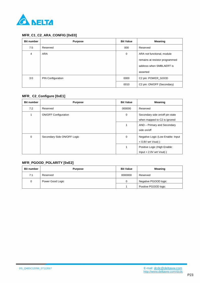
Reference to the Vo(-) terminal, there is a C2 pin. The default configuration is set to PGOOD function. And such pin can be reconfigured as secondary remote on/off pin by the PMBus interface including either negative or positive logic. Negative logic turns the module on during a logic low and off during a logic high. Positive logic turns the modules on during a logic high and off during a logic low. The secondary remote on/off can be controlled by an external switch between the on/off terminal and the Vo(-) terminal. The switch can be an open collector or open drain. MFR_C1_C2_ARA_CONFIG, MFR_ C2_LOGIC, MFR_PGOOD_POLARITY are used to config C2 pin function. Remote Sense Remote sense minimizes the effects of distribution losses by regulating the voltage at the remote-sense connections (See Figure 17). The SENSE(-) pin should be always connected to VO(-) pin. The voltage between the remote-sense pins and the output terminals must not exceed the output voltage sense range given in the Feature Specifications
[VO(+) – VO(–)] – SENSE(+) ≤0.5 V
The output voltage can also be increased by the trim, the maximum increase for the output voltage is the sum of both. The amount of power delivered by the module is defined as the voltage at the output terminals multiplied by the output current. When using remote sense and trim, the output voltage of the module can be increased, which at the same output current, would increase the power output of the module. Care should be taken to ensure that the maximum output power of the module remains at or below the maximum rated power (Maximum rated power = Vo,set x Io,max)
Vout ( + )
Load Input source
Vin ( - )
S ense ( - )
S ense ( + )
Vout ( - )
Vin ( + )
R esist ance of trace
R esist ance of trace
Figure 17: Circuit Configuration for remote sense.
Configurable Control Pins
The module contains one configurable control pins C2,
referenced to the module secondary SIG_GND. See
Mechanical Views for pin locations. The following table
list the default factory configurations for the functions
assigned to the pin.
Pin Designation/Function Configuration
C2 Power Good
Note4 Factory Default
On/OffNote5
Optional Vias PMBUS
Note4: Power Good is a Full-drive output, pull up to 3.3V internally, Note5: On/Off is an Open-drain input
Output Voltage Adjustment (TRIM) note3
To increase or decrease the output voltage set point,
connect an external resistor between the TRIM pin
and either the Vo(+) or Vo(-). The TRIM pin should be
left open if this feature is not used.
Figure 18: Circuit configuration for trim-down (decrease output voltage)
If the external resistor is connected between the TRIM and Vo (-) pins, the output voltage set point decreases (Fig. 18). The external resistor value required to obtain a percentage of output voltage
change △% is defined as:
KdownRtrim 2.10
511_
Ex. When Trim-down -10% (12V×0.9=10.8V)
KKdownRtrim 9.402.10
10
511_
DS_Q48SC12050_07112017 E-mail: [email protected]
http://www.deltaww.com/dcdc P12
Figure 19: Circuit configuration for trim-up (increase output voltage) If the external resistor is connected between the TRIM and Vo (+) the output voltage set point increases (Fig.19) The external resistor value required to obtain a percentage output voltage
change △% is defined as:
KupRtrim 2.10
511
1.225
) (100 Vo11.5_
Ex. When Trim-up +10% (12V×1.1=13.2V)
KupRtrim 3.8942.10
10
511
10225.1
)10100(1211.5_
Care should be taken to ensure that the maximum output power of the module remains at or below the maximum rated power. Note3: see the last page.
Power Good, PG The module provides a Power Good (PG) signal which is provided by the IC inside module, voltage level 3.3V, to indicate that the output voltage is within the normal output voltage range of the power module. The PG signal will be de-asserted to a low state if any condition such as overtemperature, overcurrent or loss of regulation occurs that would result in the output voltage going below the normal voltage range value. The Vout PG function could be changed via PMBUS. The command related to Vout PG function are POWER_GOOD_ON and POWER_GOOD_OFF. .
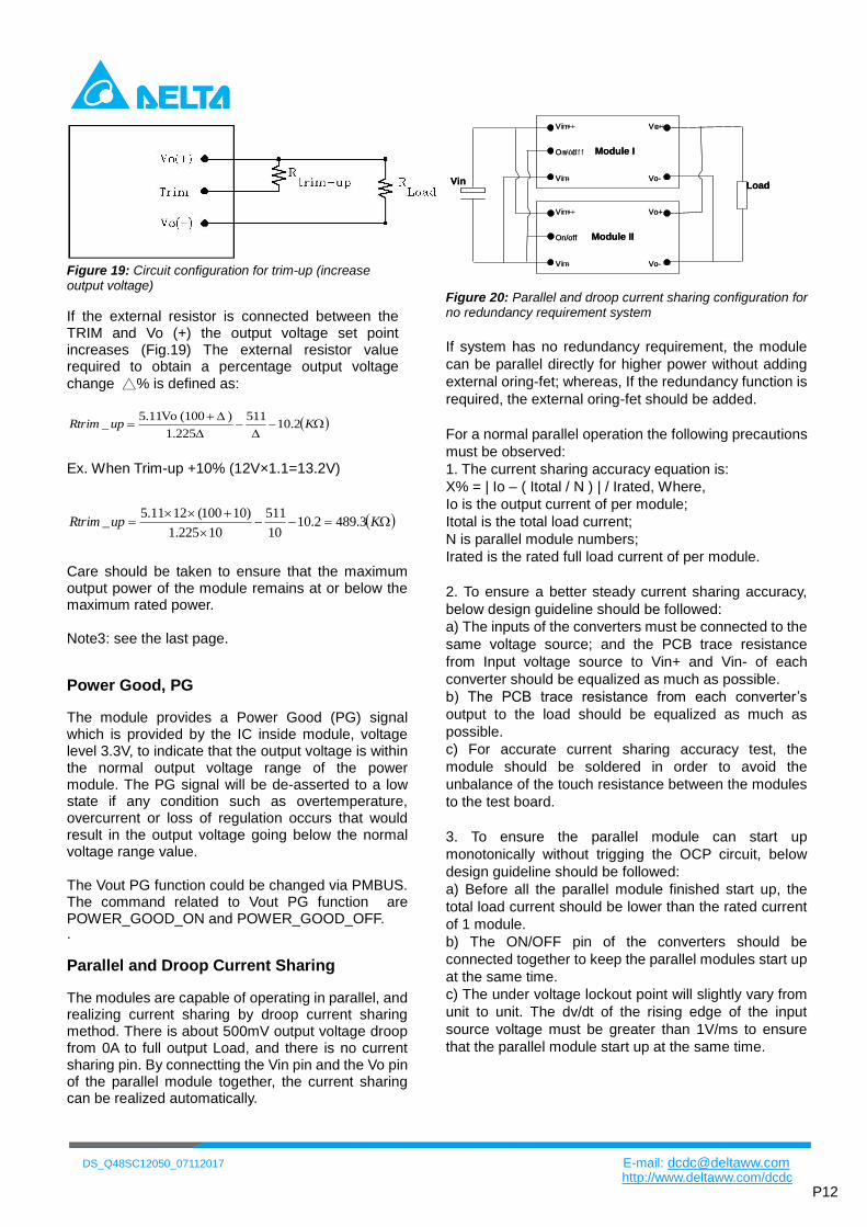
Parallel and Droop Current Sharing The modules are capable of operating in parallel, and realizing current sharing by droop current sharing method. There is about 500mV output voltage droop from 0A to full output Load, and there is no current sharing pin. By connectting the Vin pin and the Vo pin of the parallel module together, the current sharing can be realized automatically.
V i n +
V i n-
V i n +
V i n-
O n / o f f
V o +
Vo-
Module I
On/off
Vo+
Vo-
Module II
Vin Load
Vin+
Vin-
Vin+
Vin-
On/off
Vo+
Vo-
Module I
On/off
Vo+
Vo-
Module II
Vin Load
Figure 20: Parallel and droop current sharing configuration for no redundancy requirement system
If system has no redundancy requirement, the module
can be parallel directly for higher power without adding
external oring-fet; whereas, If the redundancy function is
required, the external oring-fet should be added.
For a normal parallel operation the following precautions
must be observed:
1. The current sharing accuracy equation is:
X% = | Io – ( Itotal / N ) | / Irated, Where,
Io is the output current of per module;
Itotal is the total load current;
N is parallel module numbers;
Irated is the rated full load current of per module.
2. To ensure a better steady current sharing accuracy,
below design guideline should be followed:
a) The inputs of the converters must be connected to the
same voltage source; and the PCB trace resistance
from Input voltage source to Vin+ and Vin- of each
converter should be equalized as much as possible.
b) The PCB trace resistance from each converter’s
output to the load should be equalized as much as
possible.
c) For accurate current sharing accuracy test, the
module should be soldered in order to avoid the
unbalance of the touch resistance between the modules
to the test board.
3. To ensure the parallel module can start up
monotonically without trigging the OCP circuit, below
design guideline should be followed:
a) Before all the parallel module finished start up, the
total load current should be lower than the rated current
of 1 module.
b) The ON/OFF pin of the converters should be
connected together to keep the parallel modules start up
at the same time.
c) The under voltage lockout point will slightly vary from
unit to unit. The dv/dt of the rising edge of the input
source voltage must be greater than 1V/ms to ensure
that the parallel module start up at the same time.
DS_Q48SC12050_07112017 E-mail: [email protected]
http://www.deltaww.com/dcdc P13
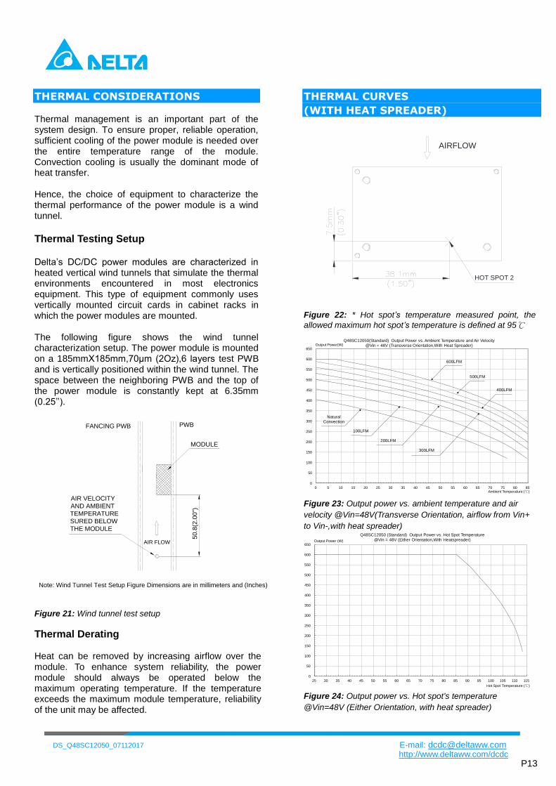
THERMAL CONSIDERATIONS Thermal management is an important part of the system design. To ensure proper, reliable operation, sufficient cooling of the power module is needed over the entire temperature range of the module. Convection cooling is usually the dominant mode of heat transfer. Hence, the choice of equipment to characterize the thermal performance of the power module is a wind tunnel.
Thermal Testing Setup Delta’s DC/DC power modules are characterized in heated vertical wind tunnels that simulate the thermal environments encountered in most electronics equipment. This type of equipment commonly uses vertically mounted circuit cards in cabinet racks in which the power modules are mounted. The following figure shows the wind tunnel characterization setup. The power module is mounted on a 185mmX185mm,70μm (2Oz),6 layers test PWB and is vertically positioned within the wind tunnel. The space between the neighboring PWB and the top of the power module is constantly kept at 6.35mm (0.25’’).
AIR FLOW
MODULE
PWB
50
.8(2
.00")
AIR VELOCITY
AND AMBIENT
TEMPERATURE
SURED BELOW
THE MODULE
FANCING PWB
Note: Wind Tunnel Test Setup Figure Dimensions are in millimeters and (Inches)
Figure 21: Wind tunnel test setup
Thermal Derating
Heat can be removed by increasing airflow over the module. To enhance system reliability, the power module should always be operated below the maximum operating temperature. If the temperature exceeds the maximum module temperature, reliability of the unit may be affected.
THERMAL CURVES
(WITH HEAT SPREADER)
AIRFLOW
HOT SPOT 2
Figure 22: * Hot spot’s temperature measured point, the
allowed maximum hot spot’s temperature is defined at 95℃
0
50
100
150
200
250
300
350
400
450
500
550
600
650
0 5 10 15 20 25 30 35 40 45 50 55 60 65 70 75 80 85
Output Power(W)
Ambient Temperature (℃)
Q48SC12050(Standard) Output Power vs. Ambient Temperature and Air Velocity
@Vin = 48V (Transverse Orientation,With Heat Spreader)
NaturalConvection
100LFM
200LFM
300LFM
500LFM
600LFM
400LFM
Figure 23: Output power vs. ambient temperature and air
velocity @Vin=48V(Transverse Orientation, airflow from Vin+
to Vin-,with heat spreader)
0
50
100
150
200
250
300
350
400
450
500
550
600
650
25 30 35 40 45 50 55 60 65 70 75 80 85 90 95 100 105 110 115
Q48SC12050 (Standard) Output Power vs. Hot Spot Temperature
@Vin = 48V (Either Orientation,With Heatspreader)
Hot Spot Temperature (℃)
Output Power (W)
Figure 24: Output power vs. Hot spot's temperature
@Vin=48V (Either Orientation, with heat spreader)
DS_Q48SC12050_07112017 E-mail: [email protected]
http://www.deltaww.com/dcdc P14
DIGITAL FEATURE DESCRIPTIONS The module has a digital PMBus interface to allow the module to be monitored, controlled and configured by the system. The module supports 4 PMBus signal lines, Data, Clock, SMBALERT (optional), Control (C2 pin, optional), and 2 Address line Addr0 and Addr1. More detail PMBus information can be found in the PMB Power Management Protocol Specification, Part I and part II, revision 1.2; which is shown in http://pmbus.org . Both 100kHz and 400kHz bus speeds are supported by the module. Connection for the PMBus interface should be following the High Power DC specifications given in section 3.1.3 in the SMBus specification V2.0 or the Low Power DC specifications in section 3.1.2. The complete SMBus specification is shown in http://smbus.org. The module supports the Packet Error Checking (PEC) protocol. It can check the PEC byte provided by the PMBus master, and include a PEC byte in all message responses to the master. And the module also can communicate with the master that does not implement the PEC mechanism. SMBALERT protocol is also supported by the module. SMBALERT line is also a wired-AND signal; by which the module can alert the PMBUS master via pulling the SMBALERT pin to an active low. There are only one way that the master and the module response to the alert of SMBALERT line. This way is for the module used in a system that does not support Alert Response Address (ARA). The module is to retain it’s resistor programmed address, when it is in an ALERT active condition. The master will communicate with the slave module using the programmed address, and using the various READ_STATUS commands to find who cause for the SMBALERT. The CLEAR_FAULTS command will clear the SMBALERT.
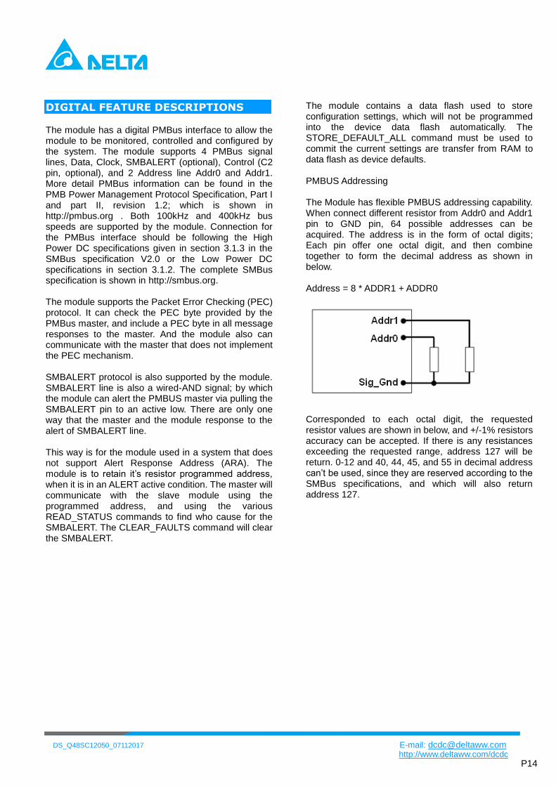
The module contains a data flash used to store configuration settings, which will not be programmed into the device data flash automatically. The STORE_DEFAULT_ALL command must be used to commit the current settings are transfer from RAM to data flash as device defaults. PMBUS Addressing The Module has flexible PMBUS addressing capability. When connect different resistor from Addr0 and Addr1 pin to GND pin, 64 possible addresses can be acquired. The address is in the form of octal digits; Each pin offer one octal digit, and then combine together to form the decimal address as shown in below. Address = 8 * ADDR1 + ADDR0
Corresponded to each octal digit, the requested resistor values are shown in below, and +/-1% resistors accuracy can be accepted. If there is any resistances exceeding the requested range, address 127 will be return. 0-12 and 40, 44, 45, and 55 in decimal address can’t be used, since they are reserved according to the SMBus specifications, and which will also return address 127.
DS_Q48SC12050_07112017 E-mail: [email protected]
http://www.deltaww.com/dcdc P15
Octal digit Resistor(Kohm)
0 10
1 15.4
2 23.7
3 36.5
4 54.9
5 84.5
6 130
7 200
PMBus Data Format
The module receives and report date in LINEAR format. The Exponent of the data words is fixed at a reasonable value for the command; altering the exponent is not supported. DIRECT format is not supported by the module. For commands that set or report any voltage thresholds related to the output voltage, the module supports the linear data format consisting of a two byte value with a 16-bit, unsigned mantissa, and a fixed exponent of -12. The format of the two data bytes is shown below:
The equation can be written as: Vout = Mantissa x 2
(-12)
For example, considering set Vout to 12V by VOUT_COMMAND, the read/write data can be calculated refer to below process: Mantissa =Vout/2
(-12)= 12/2
(-12)=49152;
Converter the calculated Mantissa to hexadecimal 0xC000.
For commands that set or report all other thresholds, including input voltages, output current, temperature, time and frequency, the supported linear data format is a two byte value with: an 11 bit, two’s complement mantissa , and a 5 bit, two’s complement exponent (scaling factor).The format of the two data bytes is shown as in below.
The equation can be written as: Value = Mantissa x 2
(exponent)
For example, considering set the turn on threshold of input under voltage lockout to 34V by VIN_ON command; the read/write data can be calculated refer to below process: Get the exponent of Vin, -3; whose binary is 11101 Mantissa =Vin/2
(-3)=34/2
(-3)=272;
Converter the calculated Mantissa to hexadecimal 110, then converter to binary 00100010000;Combine the exponent and the mantissa, 11101 and 00100010000; Converter binary 1110100100010000 to hexadecimal E910.
DS_Q48SC12050_07112017 E-mail: [email protected]
http://www.deltaww.com/dcdc P16
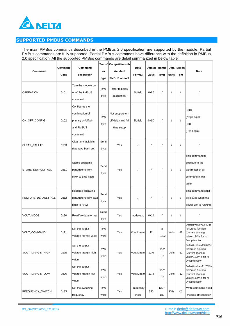
SUPPORTED PMBUS COMMANDS
The main PMBus commands described in the PMBus 2.0 specification are supported by the module. Partial PMBus commands are fully supported; Partial PMBus commands have difference with the definition in PMBus 2.0 specification. All the supported PMBus commands are detail summarized in below table
Command
Command
Code
Command
description
Transf
-er
type
Compatible with
standard
PMBUS or not?
Data
Format
Default
value
Range
limit
Data
units
Expon
-ent
Note
OPERATION 0x01
Turn the module on
or off by PMBUS
command
R/W
byte
Refer to below
description;
Bit field 0x80 / / / /
ON_OFF_CONFIG 0x02
Configures the
combination of
primary on/off pin
and PMBUS
command
R/W
byte
Not support turn
off delay and fall
time setup
Bit field 0x1D / / /
0x1D
(Neg Logic);
0x1F
(Pos Logic);
CLEAR_FAULTS 0x03
Clear any fault bits
that have been set
Send
byte
Yes / / / / / /
STORE_DEFAULT_ALL 0x11
Stores operating
parameters from
RAM to data flash
Send
byte
Yes / / / / /
This command is
effective to the
parameter of all
command in this
table.
RESTORE_DEFAULT_ALL 0x12
Restores operating
parameters from data
flash to RAM
Send
byte
Yes / / / / /
This command can't
be issued when the
power unit is running.
VOUT_MODE 0x20 Read Vo data format
Read
byte
Yes mode+exp 0x14 / / / /
VOUT_COMMAND 0x21
Set the output
voltage normal value
R/W
word
Yes Vout Linear 12
8
~13.2
Volts -12
Default value=12.4V is
for Droop function
(Current sharing),
value=12V is for no
Droop function
VOUT_MARGIN_HIGH 0x25
Set the output
voltage margin high
value
R/W
word
Yes Vout Linear 12.6
10.2
~13
Volts -12
Default value=13.02V is
for Droop function
(Current sharing),
value=12.6V is for no
Droop function
VOUT_MARGIN_LOW 0x26
Set the output
voltage margin low
value
R/W
word
Yes Vout Linear 11.4
10.2
~13
Volts -12
Default value=11.78V is
for Droop function
(Current sharing),
value=11.4V is for no
Droop function
FREQUENCY_SWITCH 0x33
Set the switching
frequency
R/W
word
Yes
Frequency
linear
130
120 ~
180
KHz -2
Write command need
module off condition
DS_Q48SC12050_07112017 E-mail: [email protected]
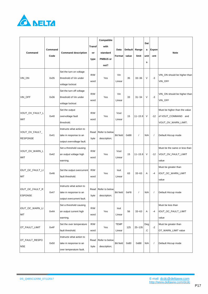
http://www.deltaww.com/dcdc P17
Command
Command
Code
Command description
Transf
-er
type
Compatible
with
standard
PMBUS or
not?
Data
Format
Default
value
Range
limit
Dat
a
unit
s
Expon
-ent
Note
VIN_ON 0x35
Set the turn on voltage
threshold of Vin under
voltage lockout
R/W
word
Yes
Vin
Linear
35 33~36 V -3
VIN_ON should be higher than
VIN_OFF
VIN_OFF 0x36
Set the turn off voltage
threshold of Vin under
voltage lockout
R/W
word
Yes
Vin
Linear
33 31~34 V -3
VIN_ON should be higher than
VIN_OFF
VOUT_OV_FAULT_L
IMIT
0x40
Set the output
overvoltage fault
threshold.
R/W
word
Yes
Vout
Linear
15 11~15.9 V -12
Must be higher than the value
of VOUT_COMMAND and
VOUT_OV_WARN_LIMIT;
VOUT_OV_FAULT_
RESPONSE
0x41
Instructs what action to
take in response to an
output overvoltage fault.
Read
byte
Refer to below
description;
Bit field 0xB8 / N/A / Default Hiccup mode
VOUT_OV_WARN_L
IMIT
0x42
Set a threshold causing
an output voltage high
warning.
R/W
word
Yes
Vout
Linear
15 11~15.9 V -12
Must be the same or less than
VOUT_OV_FAULT_LIMIT
value
IOUT_OC_FAULT_LI
MIT
0x46
Set the output overcurrent
fault threshold.
R/W
word
Yes
Iout
Linear
63 33~63 A -4
Must be greater than
IOUT_OC_WARN_LIMIT
value
IOUT_OC_FAULT_R
ESPONSE
0x47
Instructs what action to
take in response to an
output overcurrent fault.
Read
byte
Refer to below
description;
Bit field 0xF8 / N/A / Default Hiccup mode
IOUT_OC_WARN_LI
MIT
0x4A
Set a threshold causing
an output current high
warning.
R/W
word
Yes
Iout
Linear
56 33~63 A -4
Must be less than
IOUT_OC_FAULT_LIMIT
value
OT_FAULT_LIMIT 0x4F
Set the over temperature
fault threshold.
R/W
word
Yes
TEMP
Linear
125 25~135
Deg
.C
-2
Must be greater than
OT_WARN_LIMIT value
OT_FAULT_RESPO
NSE
0x50
Instructs what action to
take in response to an
over temperature fault.
Read
byte
Refer to below
description;
Bit field 0x80 0xB8 N/A / Default Hiccup mode
DS_Q48SC12050_07112017 E-mail: [email protected]
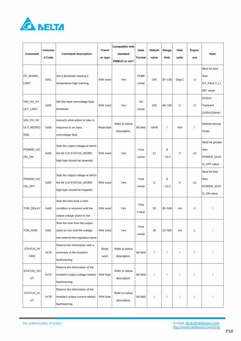
http://www.deltaww.com/dcdc P18
Command
Comman
d Code
Command description
Transf
-er type
Compatible with
standard
PMBUS or not?
Data
Format
Default
value
Range
limit
Data
units
Expon
-ent
Note
OT_WARN_
LIMIT
0x51
Set a threshold causing a
temperature high warning.
R/W word Yes
TEMP
Linear
100 25~135 Deg.C -2
Must be less
than
OT_FAULT_LI
MIT value
VIN_OV_FA
ULT_LIMIT
0x55
Set the input overvoltage fault
threshold.
R/W word Yes
Vin
Linear
100 48~100 V -3
Endure
Transient
(100V/100ms)
VIN_OV_FA
ULT_RESPO
NSE
0x56
Instructs what action to take in
response to an input
overvoltage fault.
Read byte
Refer to below
description;
Bit field 0XF8 / N/A /
Default Hiccup
mode
POWER_GO
OD_ON
0x5E
Sets the output voltage at which
the bit 3 of STATUS_WORD
high byte should be asserted.
R/W word Yes
Vout
Linear
11
8
~13.2
V -12
Must be greater
than
POWER_GOO
D_OFF value
POWER_GO
OD_OFF
0x5F
Sets the output voltage at which
the bit 3 of STATUS_WORD
high byte should be negated.
R/W word Yes
Vout
Linear
9
8
~13.2
V -12
Must be less
than
POWER_GOO
D_ON value
TON_DELAY 0x60
Sets the time from a start
condition is received until the
output voltage starts to rise
R/W word Yes
Time
Linear
20 20~500 ms -1 /
TON_RISE 0x61
Sets the time from the output
starts to rise until the voltage
has entered the regulation band.
R/W word Yes
Time
Linear
30 15~500 ms -1 /
STATUS_W
ORD
0x79
Returns the information with a
summary of the module's
fault/warning
Read
word
Refer to below
description;
Bit field / / / / /
STATUS_VO
UT
0x7A
Returns the information of the
module's output voltage related
fault/warning
R/W byte
Refer to below
description;
Bit field / / / / /
STATUS_IO
UT
0x7B
Returns the information of the
module's output current related
fault/warning
R/W byte
Refer to below
description;
Bit field / / / / /
DS_Q48SC12050_07112017 E-mail: [email protected]
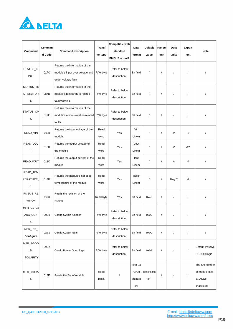
http://www.deltaww.com/dcdc P19
Command
Comman
d Code
Command description
Transf
-er type
Compatible with
standard
PMBUS or not?
Data
Format
Default
value
Range
limit
Data
units
Expon
-ent
Note
STATUS_IN
PUT
0x7C
Returns the information of the
module's input over voltage and
under voltage fault
R/W byte
Refer to below
description;
Bit field / / / / /
STATUS_TE
MPERATUR
E
0x7D
Returns the information of the
module's temperature related
fault/warning
R/W byte
Refer to below
description;
Bit field / / / / /
STATUS_CM
L
0x7E
Returns the information of the
module's communication related
faults.
R/W byte
Refer to below
description;
Bit field / / / / /
READ_VIN 0x88
Returns the input voltage of the
module
Read
word
Yes
Vin
Linear
/ / V -3 /
READ_VOU
T
0x8B
Returns the output voltage of
the module
Read
word
Yes
Vout
Linear
/ / V -12 /
READ_IOUT 0x8C
Returns the output current of the
module
Read
word
Yes
Iout
Linear
/ / A -4 /
READ_TEM
PERATURE_
1
0x8D
Returns the module's hot spot
temperature of the module
Read
word
Yes
TEMP
Linear
/ / Deg.C -2 /
PMBUS_RE
VISION
0x98
Reads the revision of the
PMBus
Read byte Yes Bit field 0x42 / / / /
MFR_C1_C2
_ARA_CONF
IG
0xE0 Config C2 pin function R/W byte
Refer to below
description;
Bit field 0x00 / / / /
MFR_ C2_
Configure
0xE1 Config C2 pin logic R/W byte
Refer to below
description;
Bit field 0x00 / / / /
MFR_PGOO
D
_POLARITY
0xE2
Config Power Good logic R/W byte
Refer to below
description;
Bit field 0x01 / / /
Default Positive
PGOOD logic
MFR_SERIA
L
0x9E Reads the SN of module
Read
block
/
Total 11
ASCII
charact
ers
‘xxxxxxxxx
xx’
/ / /
The SN number
of module use
11 ASCII
characters
DS_Q48SC12050_07112017 E-mail: [email protected]
http://www.deltaww.com/dcdc P20
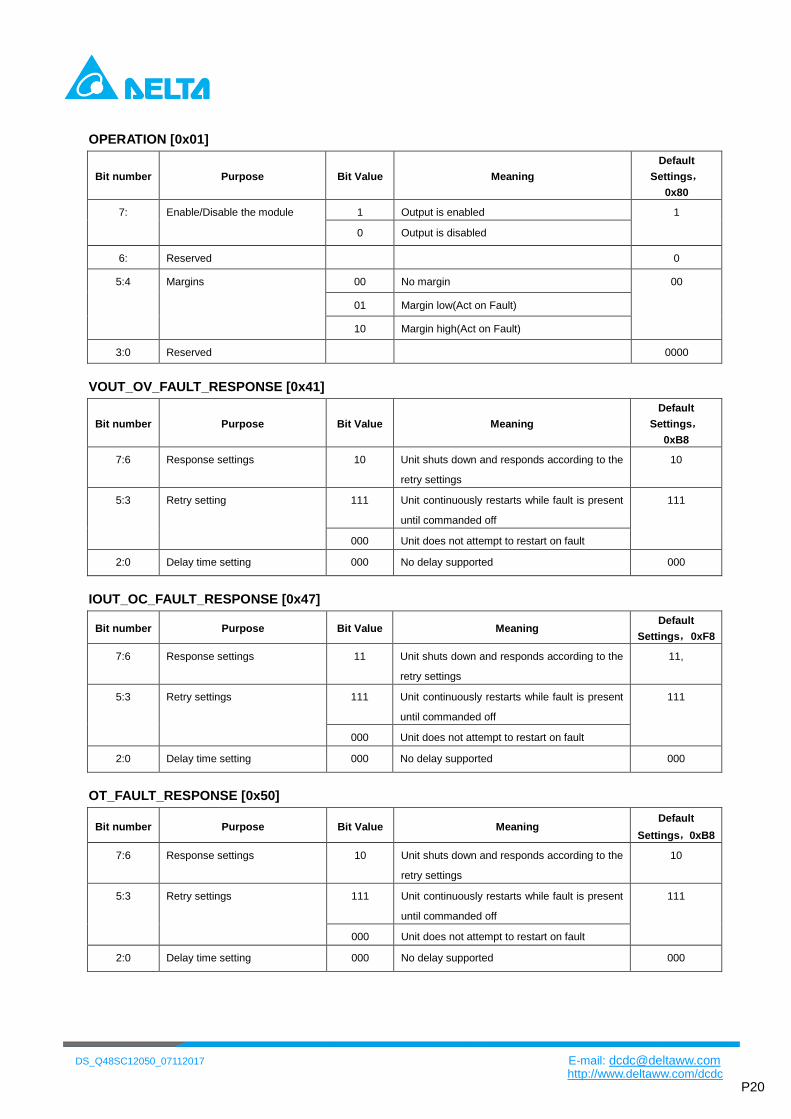
OPERATION [0x01]
Bit number Purpose Bit Value Meaning
Default
Settings,
0x80
7: Enable/Disable the module 1 Output is enabled 1
0 Output is disabled
6: Reserved 0
5:4 Margins
00 No margin 00
01 Margin low(Act on Fault)
10 Margin high(Act on Fault)
3:0 Reserved 0000
VOUT_OV_FAULT_RESPONSE [0x41]
Bit number Purpose Bit Value Meaning
Default
Settings,
0xB8
7:6 Response settings 10 Unit shuts down and responds according to the
retry settings
10
5:3 Retry setting
111 Unit continuously restarts while fault is present
until commanded off
111
000 Unit does not attempt to restart on fault
2:0 Delay time setting 000 No delay supported 000
IOUT_OC_FAULT_RESPONSE [0x47]
Bit number Purpose Bit Value Meaning Default
Settings, 0xF8
7:6 Response settings 11 Unit shuts down and responds according to the
retry settings
11,
5:3 Retry settings 111 Unit continuously restarts while fault is present
until commanded off
111
000 Unit does not attempt to restart on fault
2:0 Delay time setting 000 No delay supported 000
OT_FAULT_RESPONSE [0x50]
Bit number Purpose Bit Value Meaning Default
Settings,0xB8
7:6 Response settings 10 Unit shuts down and responds according to the
retry settings
10
5:3 Retry settings 111 Unit continuously restarts while fault is present
until commanded off
111
000 Unit does not attempt to restart on fault
2:0 Delay time setting 000 No delay supported 000
DS_Q48SC12050_07112017 E-mail: [email protected]
http://www.deltaww.com/dcdc P21
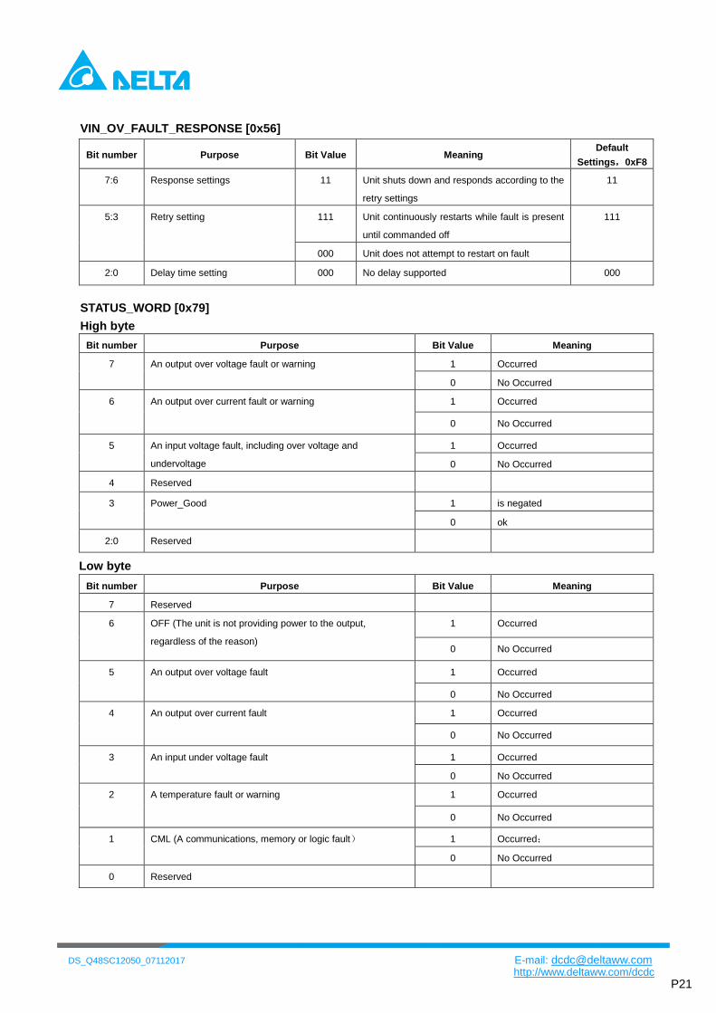
VIN_OV_FAULT_RESPONSE [0x56]
Bit number Purpose Bit Value Meaning Default
Settings,0xF8
7:6 Response settings 11 Unit shuts down and responds according to the
retry settings
11
5:3 Retry setting
111 Unit continuously restarts while fault is present
until commanded off
111
000 Unit does not attempt to restart on fault
2:0 Delay time setting 000 No delay supported 000
STATUS_WORD [0x79]
High byte
Bit number Purpose Bit Value Meaning
7 An output over voltage fault or warning 1 Occurred
0 No Occurred
6 An output over current fault or warning 1 Occurred
0 No Occurred
5 An input voltage fault, including over voltage and
undervoltage
1 Occurred
0 No Occurred
4 Reserved
3 Power_Good 1 is negated
0 ok
2:0 Reserved
Low byte
Bit number Purpose Bit Value Meaning
7 Reserved
6 OFF (The unit is not providing power to the output,
regardless of the reason)
1 Occurred
0 No Occurred
5 An output over voltage fault 1 Occurred
0 No Occurred
4 An output over current fault 1 Occurred
0 No Occurred
3 An input under voltage fault 1 Occurred
0 No Occurred
2 A temperature fault or warning 1 Occurred
0 No Occurred
1 CML (A communications, memory or logic fault) 1 Occurred;
0 No Occurred
0 Reserved
DS_Q48SC12050_07112017 E-mail: [email protected]
http://www.deltaww.com/dcdc P22
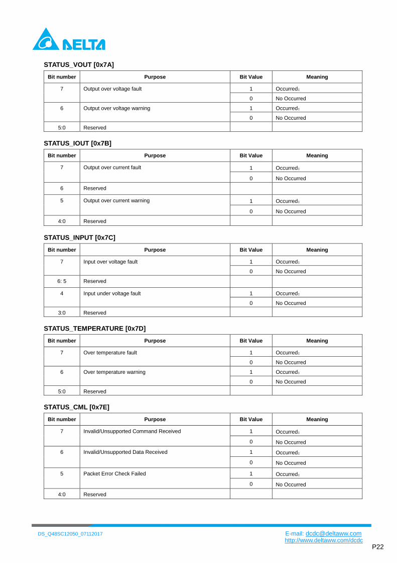
STATUS_VOUT [0x7A]
Bit number Purpose Bit Value Meaning
7
Output over voltage fault 1 Occurred;
0 No Occurred
6 Output over voltage warning 1 Occurred;
0 No Occurred
5:0 Reserved
STATUS_IOUT [0x7B]
Bit number Purpose Bit Value Meaning
7
Output over current fault 1 Occurred;
0 No Occurred
6 Reserved
5 Output over current warning 1 Occurred;
0 No Occurred
4:0 Reserved
STATUS_INPUT [0x7C]
Bit number Purpose Bit Value Meaning
7
Input over voltage fault 1 Occurred;
0 No Occurred
6: 5 Reserved
4 Input under voltage fault 1 Occurred;
0 No Occurred
3:0 Reserved
STATUS_TEMPERATURE [0x7D]
Bit number Purpose Bit Value Meaning
7
Over temperature fault 1 Occurred;
0 No Occurred
6 Over temperature warning 1 Occurred;
0 No Occurred
5:0 Reserved
STATUS_CML [0x7E]
Bit number Purpose Bit Value Meaning
7
Invalid/Unsupported Command Received 1 Occurred;
0 No Occurred
6 Invalid/Unsupported Data Received 1 Occurred;
0 No Occurred
5 Packet Error Check Failed 1 Occurred;
0 No Occurred
4:0 Reserved
DS_Q48SC12050_07112017 E-mail: [email protected]
http://www.deltaww.com/dcdc P23
MFR_C1_C2_ARA_CONFIG [0xE0]
Bit number Purpose Bit Value Meaning
7:5 Reserved 000 Reserved
4 ARA 0 ARA not functional, module
remains at resistor programmed
address when SMBLAERT is
asserted
3:0 PIN Configuration 0000 C2 pin: POWER_GOOD
0010 C2 pin: ON/OFF (Secondary)
MFR_ C2_Configure [0xE1]
Bit number Purpose Bit Value Meaning
7:2 Reserved 000000 Reserved
1 ON/OFF Configuration 0 Secondary side on/off pin state
when mapped to C2 is ignored
1 AND – Primary and Secondary
side on/off
0 Secondary Side ON/OFF Logic 0 Negative Logic (Low Enable: Input
< 0.8V wrt Vout(-)
1 Positive Logic (High Enable:
Input > 2.0V wrt Vout(-)
MFR_PGOOD_POLARITY [0xE2]
Bit number Purpose Bit Value Meaning
7:1 Reserved 0000000 Reserved
0 Power Good Logic 0 Negative PGOOD logic
1 Positive PGOOD logic
DS_Q48SC12050_07112017 E-mail: [email protected]
http://www.deltaww.com/dcdc P24
MECHANICAL DRAWING( WITH HEAT-SPREADER)
*For modules with through-hole pins and the optional heat spreader, they are intended for wave
soldering assembly onto system boards, please do not subject such modules through reflow
temperature profile.
Pin Specification:
Pins 1-4, 6~8 1.00mm (0.040”) diameter (All pins are copper with matte Tin plating over Nickel under plating) Pins 5,9 2. 1.50mm (0.059”) diameter (All pins are copper with matte Tin plating over Nickel under plating) Pins 10-16 1. SQ 0.50mm(0.020’’) ( All pins are copper with gold flash plating)
DS_Q48SC12050_07112017 E-mail: [email protected]
http://www.deltaww.com/dcdc P26
PART NUMBERING SYSTEM
Q 48 S C 120 50 N R D H
Type of
Product
Input
Voltage
Number of
Outputs
Product
Series
Output
Voltage
Output
Current
ON/OFF
Logic
Pin Length
/Type
Pin
Assignment Option Code
Q - Quarter
Brick
48 -
36~75V
S -
Single
C -
Series number
120 - 12V
50 - 50A P -
Positive
N -
Negative
R- 0.170”
N- 0.145”
K- 0.110”
D -
Digital pins
A -
Analog pins
I -
IBC pins
T -
Trim pins
Trim Pin Current
sharing
Heat
spreader Case pin
H Yes No Yes No
I No Droop Yes No
J No No Yes No
R Yes No Yes Yes
S No Droop Yes Yes
T No No Yes Yes
Note for mechanical pins option:
1. D- Digital pins*: with digital pins & sense pins & PG function.
2. A- Analog pins*: with sense pins, without digital pins
3. I- IBC pins*: without digital pins & sense pins
4. T- Trim pins: with digital pins, without sense pins
MODEL LIST
MODEL NAME INPUT OUTPUT EFF @
100%LOAD
Q48SC12050NRDH 36V~75V 19A 12V 50A 94.2%
Note3: If use VOUT_COMMAND of PMBUS to trim Vout set point, then the function of trim pin(7 pin) will be disabled
immediately. And if need enable the function of trim pin(7 pin) to trim Vout set point again, should turn off and turn on the
input voltage of module to restart module.
CONTACT: www.deltaww.com/dcdc Email: [email protected]
USA:
Telephone: East Coast: 978-656-3993 West Coast: 510-668-5100
Europe:
Phone: +31-20-655-0967
Asia & the rest of world:
Telephone: +886 3 4526107 ext 6220~6224
WARRANTY
Delta offers a two (2) year limited warranty. Complete warranty information is listed on our web site or is available upon request from Delta.
Information furnished by Delta is believed to be accurate and reliable. However, no responsibility is assumed by Delta for its use, nor for any infringements of patents or other rights of third parties, which may result from its use. No license is granted by implication or otherwise under any patent or patent rights of Delta. Delta reserves the right to revise these specifications at any time, without notice.