Embed Size (px)
Citation preview
DE58/DC58/DE108/DC108 LOGIC DESIGN DEC 2015
© IETE 1
Q.2 a. What is a Digital System? Explain the advantages and limitations of Digital Techniques over Analog Techniques. (8)
Answer: Digital System: A digital system is a combination of devices designed to manipulate logical information or physical quantities that are represented in digital form i.e., the quantities can take on only discrete values. Advantages of Digital Techniques over Analog Techniques: (i) Digital systems are generally easier to design: The circuits used in digital systems are
switching circuits, where exact values of voltage or current are not important, only the range (HIGH or LOW) in which they fall.
(ii) Information storage is easy: This is accomplished by special devices and circuits that can latch onto digital information and hold it for as long as necessary and mass storage techniques that can store billions of bits of information in a relatively small physical space. Analog storage capabilities are extremely limited.
(iii) Accuracy and precision are easier to maintain throughout the system: Once a signal is digitized, the information it contains does not deteriorate as it is processed. In analog systems, the voltage an current signals tend to be distorted by the effects of temperature, humidity and component tolerance variations in the circuits that process the signal.
(iv) Operation can be programmed: It is fairly easy to design digital systems whose operation is controlled by a set of stored instructions called a program. Analog systems can also be programmed, but the variety and the complexity of the available operations are severely limited.
(v) Digital circuits are less affected by noise: Spurious fluctuations in voltage (noise) are not as critical digital systems because the exact value of a voltage is not important, as long as the noise in not large enough to prevent us from distinguishing a HIGH from a LOW.
(vi) More digital circuitry can be fabricated on IC chips: More amount of digital circuitry are fabricated on IC chip, whereas analog circuitry has complexity with the use of devices that cannot be economically integrated (high value capacitors, precision resistors, inductors, transformers) have prevented analog systems from achieving the same high degree of integration.
Limitations of Digital Techniques over Analog Techniques:
(i) The real world is analog. (ii) Processing digitized signals takes time.
b. Convert the decimal number 82.67 to its equivalent binary number. (4) Answer:
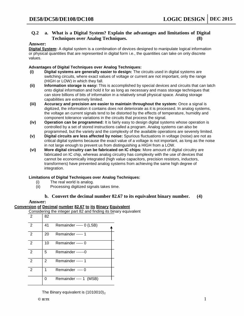
Conversion of Decimal number 82.67 to its Binary Equivalent Considering the integer part 82 and finding its binary equivalent
The Binary equivalent is (1010010)2
2 82
2 41 Remainder ----- 0 (LSB)
2 20 Remainder ----- 1
2 10 Remainder ----- 0
2 5 Remainder ------0
2 2 Remainder ----- 1
2 1 Remainder ---- 0
0 Remainder ---- 1 (MSB)
DE58/DC58/DE108/DC108 LOGIC DESIGN DEC 2015
© IETE 2
Now taking the fractional part i.e., 0.67 Fraction
Fraction X 2 Remainder New Fraction
Integer
0.67 1.34 0.34 1
0.34 0.68 0.68 0
0.68 1.36 0.36 1
0.36 0.72 0.72 0
0.72 1.44 0.44 1
0.44 0.88 0.88 0
0.88 1.76 0.76 1
0.76 1.52 0.52 1
It is seen that, it is not possible to get a zero as remainder even after 8 stages. The process continued further on an approximation can be made and the process is terminated here.
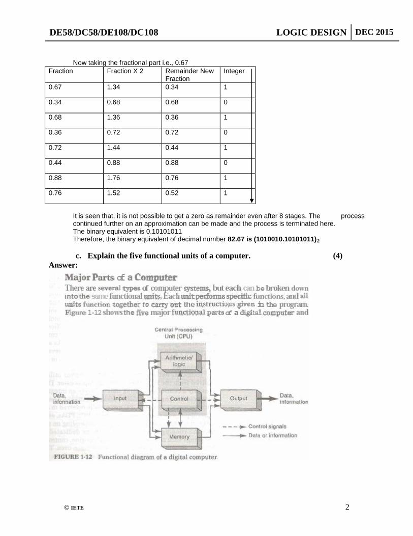
The binary equivalent is 0.10101011 Therefore, the binary equivalent of decimal number 82.67 is (1010010.10101011)2 c. Explain the five functional units of a computer. (4) Answer:
DE58/DC58/DE108/DC108 LOGIC DESIGN DEC 2015
© IETE 3
Q.3 a. Simplify the logic expression F = ABC + AB C + A BC + A BC + A B C using boolean algebraic theorems. (6) Answer: Simplification of the logic expression F = ABC + AB C + A B C + A BC + A B C F = ABC + AB C + A BC + A BC + A B C
F = A + B + C + ( A + B )C + A B C + A ( B + C ) + A B C
( ABC = A + B + C and AB = A + B by using Demorgan’s Laws)
= A + B + C + A C + B C + A B C + A B + A C + A B C
= A + A C+ B + B C + C + A C + A B C +A B + A B C
= A (1+C)+ B (1 + C) + C (1 + A) + A B C + A B + A B C
= A + B + C + A B C + A B + A B C { (1+C) = 1 and (1+A) = 1}
= ( A + A B ) + B (1 + AC) + C (1+ A B)
= ( A + B )+ B + C { ( A + A B ) = ( A + B ); (1+AC) = 1 and (1+ A B) =1}
F = ( A + B + C ) ( B + B = B ) b. Draw the logic diagram for 4-bit Even Parity Generator and explain its
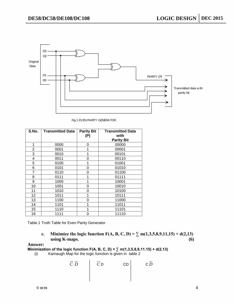
operation. (4) Answer: ) 4-bit Even Parity Generator: Fig.(1) show the logic diagram of 4-bit Even parity Generator, where a group of four bits as the data to be transmitted. The set of data to be transmitted is applied to the parity-generator circuit, which produces the even-parity bit, P at its output. The transmitted from the binary number from 0000 to 1111 and its parity bit is shown in the truth table of Table.1. The transmitted data is the summation of transmitted data and parity bit is also shown in Table.1.This parity bit is transmitted to the receiver along with the original data bits, making a total of five bits.
DE58/DC58/DE108/DC108 LOGIC DESIGN DEC 2015
© IETE 4
S.No. Transmitted Data Parity Bit (P)
Transmitted Data with
Parity Bit 1 0000 0 00000 2 0001 1 00001 3 0010 1 00101 4 0011 0 00110 5 0100 1 01001 6 0101 0 01010 7 0110 0 01100 8 0111 1 01111 9 1000 1 10001 10 1001 0 10010 11 1010 0 10100 12 1011 1 10111 13 1100 0 11000 14 1101 1 11011 15 1110 1 11101 16 1111 0 11110
Table.1 Truth Table for Even Parity Generator
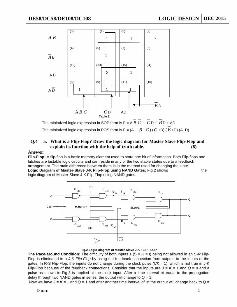
c. Minimize the logic function F(A, B, C, D) = ∑ m(1,3,5,8,9,11,15) + d(2,13) using K-maps. (6) Answer: Minimization of the logic function F(A, B, C, D) = ∑ m(1,3,5,8,9,11.15) + d(2,13)
(i) Karnaugh Map for the logic function is given in table 2 C D C D CD C D
PARITY (P)
Transmitted data w ith parity bit
D0D1
D2D3
Original Data
Fig.1 EVEN PARITY GENERATOR
DE58/DC58/DE108/DC108 LOGIC DESIGN DEC 2015
© IETE 5
A B A B
A B
A B
B D A B C C D AD Table 2
The minimized logic expression in SOP form is F = A B C + C D + B D + AD
The minimized logic expression in POS form is F = (A + B + C ) ( C +D) ( B +D) (A+D)
Q.4 a. What is a Flip-Flop? Draw the logic diagram for Master Slave Flip-Flop and explain its function with the help of truth table. (8)
Answer: Flip-Flop: A flip-flop is a basic memory element used to store one bit of information. Both Flip-flops and latches are bistable logic circuits and can reside in any of the two stable states due to a feedback arrangement. The main difference between them is in the method used for changing the state.
Logic Diagram of Master-Slave J-K Flip-Flop using NAND Gates: Fig.2 shows the logic diagram of Master-Slave J-K Flip-Flop using NAND gates.
J
K
CLK
G
G
G
G
G
G
G
G
3M
4M
1M
2M
3S
4S
1S
2S
PR
CLR
QM
_Q
M
___CLK
Q
_Q
SS
R S
MASTER SLAVE
Fig.2 Logic Diagram of Master-Slave J-K FLIP-FLOP
The Race-around Condition: The difficulty of both inputs 1 (S = R = I) being not allowed in an S-R Flip-Flop is eliminated in a J-K Flip-Flop by using the feedback connection from outputs to the inputs of the gates. In R-S Flip-Flop, the inputs do not change during the clock pulse (CK = 1), which is not true in J-K Flip-Flop because of the feedback connections. Consider that the inputs are J = K = 1 and Q = 0 and a pulse as shown in Fig.3 is applied at the clock input. After a time interval ∆t equal to the propagation delay through two NAND gates in series, the output will change to Q = 1. Now we have J = K = 1 and Q = 1 and after another time interval of ∆t the output will change back to Q =
(0)
(1) 1
(3) 1
(2) X
(4) (5) 1
(7)
(6)
(12) (13) X
(15) 1
(!4)
(8) 1
(9) 1
(11) 1
(10)
DE58/DC58/DE108/DC108 LOGIC DESIGN DEC 2015
© IETE 6
O. Hence, for the duration tp of the clock pulse, the output will oscillate back and forth between 0 and 1. At the end of the clock pulse, the value of Q is uncertain. This situation is referred to as the race-around condition. The race-around condition can be avoided if tp < ∆t < T. However, it may be difficult to satisfy this inequality because of very small propagation delays in ICs. A more practical method of overcoming this difficulty is the use of the master-slave (M-S) configuration.
tP
0 T
LEADING (POSITIVE) EDGE
TRAILING (NEGATIVE) EDGE
Fig.3 a Clock Pulse
A master-slave J-K Flip-Flop is a cascade of two S-R Flip-Flops with feedback from the outputs of the second to the inputs to the first as illustrated in Fig.2. Positive clock pulses are applied to the first Flip-Flop and the clock pulses are inverted before these are applied to the second Flip-Flop. When CK=1, the first Flop-Flop is enabled and the outputs QM and MQ respond to their inputs J and K according the
Table 7.1. At this time, the second Flip-Flop is inhibited because its clock is LOW ( CK = 0). When CK
goes LOW (CK = 1), the first Flop-Flop is inhibited and the second Flip-Flop is enabled, because now its
clock is HIGH (CK = 1). Therefore, the outputs Q and Q Follow the outputs QM and MQ respective (second and third rows of Table 3). Since the second Flip-Flop simply follows the first one, it is referred to as the Slave and the first one as the Master. Hence, this configuration is referred to as Master-Slave Flip-Flop. In this circuit, the inputs to the gates G3M and G4M do not change during the clock pulse, therefore the Race-around condition does not exist. The state of the Master-Slave Flip-Flop changes at the negative transition (trailing end).
Inputs
Output
PR
CLR
CLK
J
K
Q
0
0
X
X
X
Race Condition
0
1
X
X
X
1
1
0
X
X
X
0
1
1
X
0
0
No change
1
1
0
1
0
1
1
1
0
1
1
1
1
1
Toggle
Table 3 Truth Table of JK Master-Slave Flip-Flop
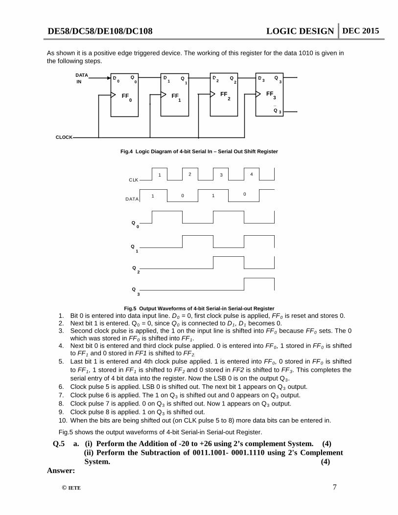
b. Explain the application of Flip-Flop as a Shift Register using D Flip-Flops. (8)
Answer: Application of Flip-Flop as a Shift Register (SERIAL IN - SERIAL OUT SHIFT REGISTER) using D Flip-Flops;
4 shows a 4 bit serial in - serial out shift register consisting of four D flip flops FF0 , FF1 , FF2 and FF3.
DE58/DC58/DE108/DC108 LOGIC DESIGN DEC 2015
© IETE 7
As shown it is a positive edge triggered device. The working of this register for the data 1010 is given in the following steps.
D Q D QD Q D Q0 0 1 1 2 2 3 3
FF FF FF FF1 2 30
DATA IN
CLOCK
_Q 3
Fig.4 Logic Diagram of 4-bit Serial In – Serial Out Shift Register
1 2 3 4
Q
Q
Q
Q
0
1
2
3
CLK
DATA1 0 1 0
Fig.5 Output Waveforms of 4-bit Serial-in Serial-out Register
1. Bit 0 is entered into data input line. D0 = 0, first clock pulse is applied, FF0 is reset and stores 0. 2. Next bit 1 is entered. Q0 = 0, since Q0 is connected to D1, D1 becomes 0. 3. Second clock pulse is applied, the 1 on the input line is shifted into FF0 because FF0 sets. The 0
which was stored in FF0 is shifted into FF1. 4. Next bit 0 is entered and third clock pulse applied. 0 is entered into FF0, 1 stored in FF0 is shifted
to FF1 and 0 stored in FF1 is shifted to FF2. 5. Last bit 1 is entered and 4th clock pulse applied. 1 is entered into FF0, 0 stored in FF0 is shifted
to FF1, 1 stored in FF1 is shifted to FF2 and 0 stored in FF2 is shifted to FF3. This completes the serial entry of 4 bit data into the register. Now the LSB 0 is on the output Q3.
6. Clock pulse 5 is applied. LSB 0 is shifted out. The next bit 1 appears on Q3 output. 7. Clock pulse 6 is applied. The 1 on Q3 is shifted out and 0 appears on Q3 output. 8. Clock pulse 7 is applied. 0 on Q3 is shifted out. Now 1 appears on Q3 output. 9. Clock pulse 8 is applied. 1 on Q3 is shifted out. 10. When the bits are being shifted out (on CLK pulse 5 to 8) more data bits can be entered in.
Fig.5 shows the output waveforms of 4-bit Serial-in Serial-out Register.
Q.5 a. (i) Perform the Addition of -20 to +26 using 2’s complement System. (4) (ii) Perform the Subtraction of 0011.1001- 0001.1110 using 2's Complement
System. (4) Answer:
DE58/DC58/DE108/DC108 LOGIC DESIGN DEC 2015
© IETE 8
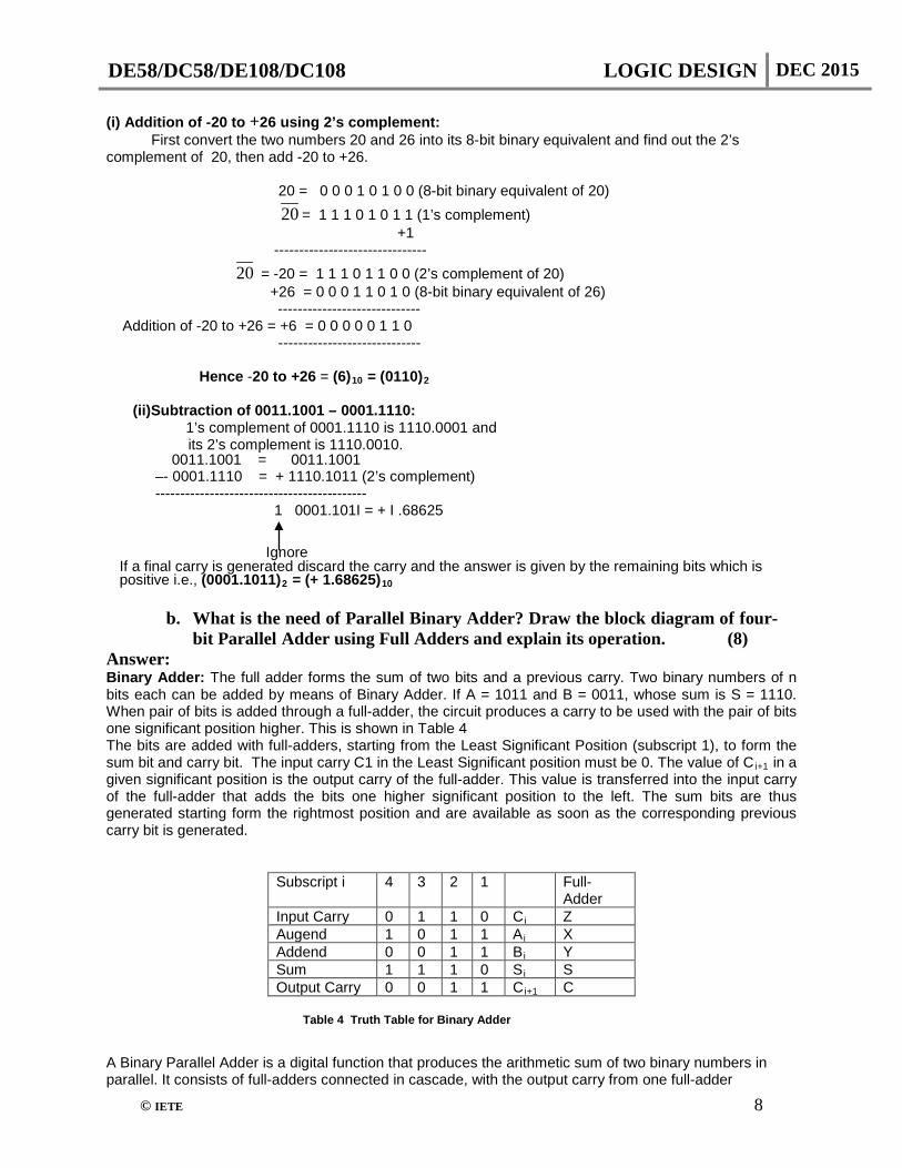
(i) Addition of -20 to +26 using 2’s complement: First convert the two numbers 20 and 26 into its 8-bit binary equivalent and find out the 2’s complement of 20, then add -20 to +26. 20 = 0 0 0 1 0 1 0 0 (8-bit binary equivalent of 20) 20 = 1 1 1 0 1 0 1 1 (1’s complement) +1 ------------------------------- 20 = -20 = 1 1 1 0 1 1 0 0 (2’s complement of 20) +26 = 0 0 0 1 1 0 1 0 (8-bit binary equivalent of 26) ----------------------------- Addition of -20 to +26 = +6 = 0 0 0 0 0 1 1 0 ----------------------------- Hence -20 to +26 = (6)10 = (0110)2
(ii)Subtraction of 0011.1001 – 0001.1110: 1’s complement of 0001.1110 is 1110.0001 and
its 2’s complement is 1110.0010. 0011.1001 = 0011.1001 –- 0001.1110 = + 1110.1011 (2’s complement) ------------------------------------------- 1 0001.101I = + I .68625
Ignore
If a final carry is generated discard the carry and the answer is given by the remaining bits which is positive i.e., (0001.1011)2 = (+ 1.68625)10
b. What is the need of Parallel Binary Adder? Draw the block diagram of four-bit Parallel Adder using Full Adders and explain its operation. (8)
Answer: Binary Adder: The full adder forms the sum of two bits and a previous carry. Two binary numbers of n
bits each can be added by means of Binary Adder. If A = 1011 and B = 0011, whose sum is S = 1110. When pair of bits is added through a full-adder, the circuit produces a carry to be used with the pair of bits one significant position higher. This is shown in Table 4
The bits are added with full-adders, starting from the Least Significant Position (subscript 1), to form the sum bit and carry bit. The input carry C1 in the Least Significant position must be 0. The value of Ci+1 in a given significant position is the output carry of the full-adder. This value is transferred into the input carry of the full-adder that adds the bits one higher significant position to the left. The sum bits are thus generated starting form the rightmost position and are available as soon as the corresponding previous carry bit is generated.
Subscript i 4 3 2 1 Full-Adder
Input Carry 0 1 1 0 Ci Z Augend 1 0 1 1 Ai X Addend 0 0 1 1 Bi Y Sum 1 1 1 0 Si S Output Carry 0 0 1 1 Ci+1 C
Table 4 Truth Table for Binary Adder A Binary Parallel Adder is a digital function that produces the arithmetic sum of two binary numbers in parallel. It consists of full-adders connected in cascade, with the output carry from one full-adder
DE58/DC58/DE108/DC108 LOGIC DESIGN DEC 2015
© IETE 9
connected to the input carry of the next full-adder. Fig.6 shows a 4-bit Binary Parallel Adder. The augend bits of A and the addend bits of the B are designated by subscript numbers from right to left, with subscript 1 denoting the low-order bit. The carries are connected in a chain through the full-adders. The input carry to the adder is C1 and the output carry is C5. The S outputs generate the required sum bits.
CC C C
C 1234
5
SSSS 1234
AAAA BBBB11223344
FULLADDER
FULLADDER
FULLADDER
FULLADDER
Fig.6 4-bit Binary Parallel Adder using Full-Adders
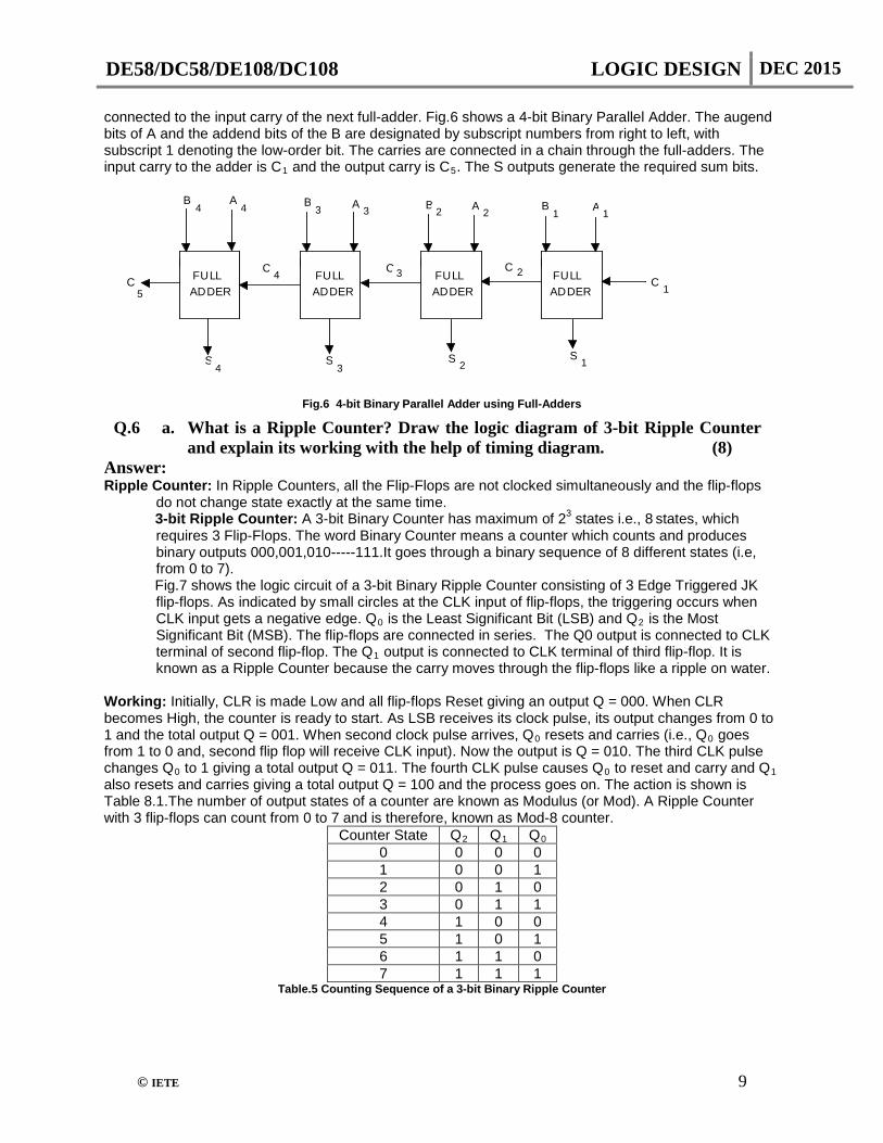
Q.6 a. What is a Ripple Counter? Draw the logic diagram of 3-bit Ripple Counter and explain its working with the help of timing diagram. (8)
Answer: Ripple Counter: In Ripple Counters, all the Flip-Flops are not clocked simultaneously and the flip-flops
do not change state exactly at the same time. 3-bit Ripple Counter: A 3-bit Binary Counter has maximum of 23 states i.e., 8 states, which
requires 3 Flip-Flops. The word Binary Counter means a counter which counts and produces binary outputs 000,001,010-----111.It goes through a binary sequence of 8 different states (i.e, from 0 to 7).
Fig.7 shows the logic circuit of a 3-bit Binary Ripple Counter consisting of 3 Edge Triggered JK flip-flops. As indicated by small circles at the CLK input of flip-flops, the triggering occurs when CLK input gets a negative edge. Q0 is the Least Significant Bit (LSB) and Q2 is the Most Significant Bit (MSB). The flip-flops are connected in series. The Q0 output is connected to CLK terminal of second flip-flop. The Q1 output is connected to CLK terminal of third flip-flop. It is known as a Ripple Counter because the carry moves through the flip-flops like a ripple on water.
Working: Initially, CLR is made Low and all flip-flops Reset giving an output Q = 000. When CLR
becomes High, the counter is ready to start. As LSB receives its clock pulse, its output changes from 0 to 1 and the total output Q = 001. When second clock pulse arrives, Q0 resets and carries (i.e., Q0 goes from 1 to 0 and, second flip flop will receive CLK input). Now the output is Q = 010. The third CLK pulse changes Q0 to 1 giving a total output Q = 011. The fourth CLK pulse causes Q0 to reset and carry and Q1 also resets and carries giving a total output Q = 100 and the process goes on. The action is shown is Table 8.1.The number of output states of a counter are known as Modulus (or Mod). A Ripple Counter with 3 flip-flops can count from 0 to 7 and is therefore, known as Mod-8 counter.
Counter State Q2 Q1 Q0 0 0 0 0 1 0 0 1 2 0 1 0 3 0 1 1 4 1 0 0 5 1 0 1 6 1 1 0 7 1 1 1
Table.5 Counting Sequence of a 3-bit Binary Ripple Counter
DE58/DC58/DE108/DC108 LOGIC DESIGN DEC 2015
© IETE 10
J J J
K K K
0
0
1
1
2
2
Q Q Q0 1 2
FF FF FF10 2
Q Q Q0 1 2
CLEAR
Cr Cr Cr
HIGH
CLOCKPULSES
Fig.7 Logic Diagram of 3-Bit Binary Ripple Counter
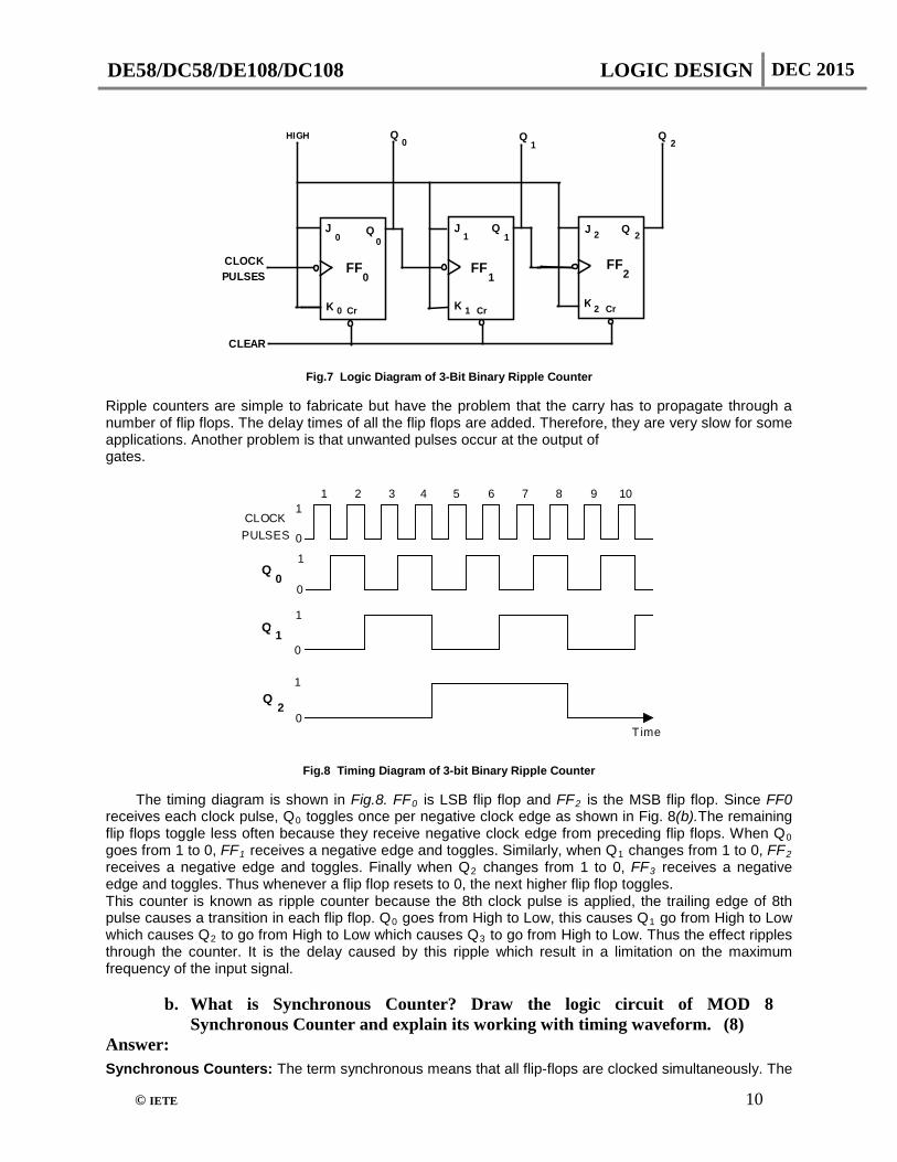
Ripple counters are simple to fabricate but have the problem that the carry has to propagate through a number of flip flops. The delay times of all the flip flops are added. Therefore, they are very slow for some applications. Another problem is that unwanted pulses occur at the output of gates.
1 2 3 4 5 6 7 8 9 10
CLOCKPULSES
1
1
1
1
0
0
0
0
Q
Q
Q
0
1
2
Time
Fig.8 Timing Diagram of 3-bit Binary Ripple Counter
The timing diagram is shown in Fig.8. FF0 is LSB flip flop and FF2 is the MSB flip flop. Since FF0
receives each clock pulse, Q0 toggles once per negative clock edge as shown in Fig. 8(b).The remaining flip flops toggle less often because they receive negative clock edge from preceding flip flops. When Q0 goes from 1 to 0, FF1 receives a negative edge and toggles. Similarly, when Q1 changes from 1 to 0, FF2 receives a negative edge and toggles. Finally when Q2 changes from 1 to 0, FF3 receives a negative edge and toggles. Thus whenever a flip flop resets to 0, the next higher flip flop toggles. This counter is known as ripple counter because the 8th clock pulse is applied, the trailing edge of 8th pulse causes a transition in each flip flop. Q0 goes from High to Low, this causes Q1 go from High to Low which causes Q2 to go from High to Low which causes Q3 to go from High to Low. Thus the effect ripples through the counter. It is the delay caused by this ripple which result in a limitation on the maximum frequency of the input signal. b. What is Synchronous Counter? Draw the logic circuit of MOD 8
Synchronous Counter and explain its working with timing waveform. (8) Answer: Synchronous Counters: The term synchronous means that all flip-flops are clocked simultaneously. The
DE58/DC58/DE108/DC108 LOGIC DESIGN DEC 2015
© IETE 11
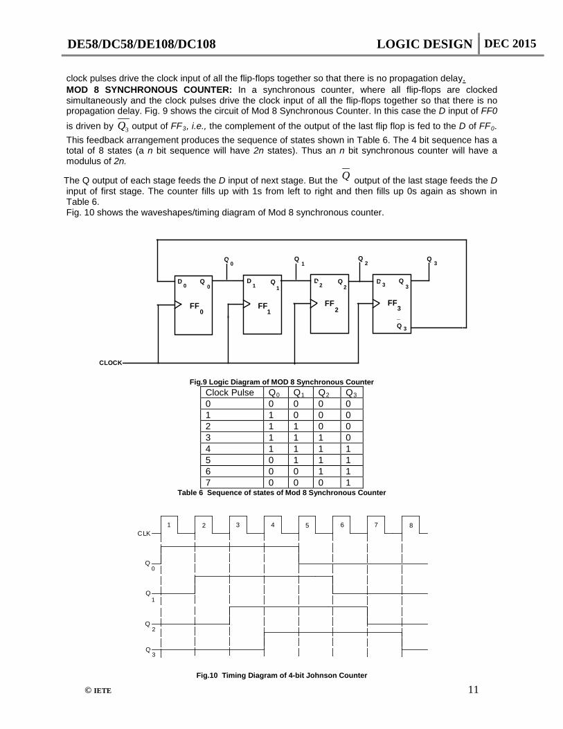
clock pulses drive the clock input of all the flip-flops together so that there is no propagation delay. MOD 8 SYNCHRONOUS COUNTER: In a synchronous counter, where all flip-flops are clocked
simultaneously and the clock pulses drive the clock input of all the flip-flops together so that there is no propagation delay. Fig. 9 shows the circuit of Mod 8 Synchronous Counter. In this case the D input of FF0 is driven by 3Q output of FF3, i.e., the complement of the output of the last flip flop is fed to the D of FF0. This feedback arrangement produces the sequence of states shown in Table 6. The 4 bit sequence has a total of 8 states (a n bit sequence will have 2n states). Thus an n bit synchronous counter will have a modulus of 2n.
The Q output of each stage feeds the D input of next stage. But the Q output of the last stage feeds the D input of first stage. The counter fills up with 1s from left to right and then fills up 0s again as shown in Table 6.
Fig. 10 shows the waveshapes/timing diagram of Mod 8 synchronous counter.
D D QD Q D Q0 0 1 1 2 2 3 3
FF FF FF FF1 2 30
CLOCK
_Q 3
Q
Q Q Q Q0 1 2 3
Fig.9 Logic Diagram of MOD 8 Synchronous Counter
Clock Pulse Q0 Q1 Q2 Q3 0 0 0 0 0 1 1 0 0 0 2 1 1 0 0 3 1 1 1 0 4 1 1 1 1 5 0 1 1 1 6 0 0 1 1 7 0 0 0 1
Table 6 Sequence of states of Mod 8 Synchronous Counter
1 2 3 4 5 6 7 8
Q
Q
Q
Q
0
1
2
3
CLK
Fig.10 Timing Diagram of 4-bit Johnson Counter
DE58/DC58/DE108/DC108 LOGIC DESIGN DEC 2015
© IETE 12
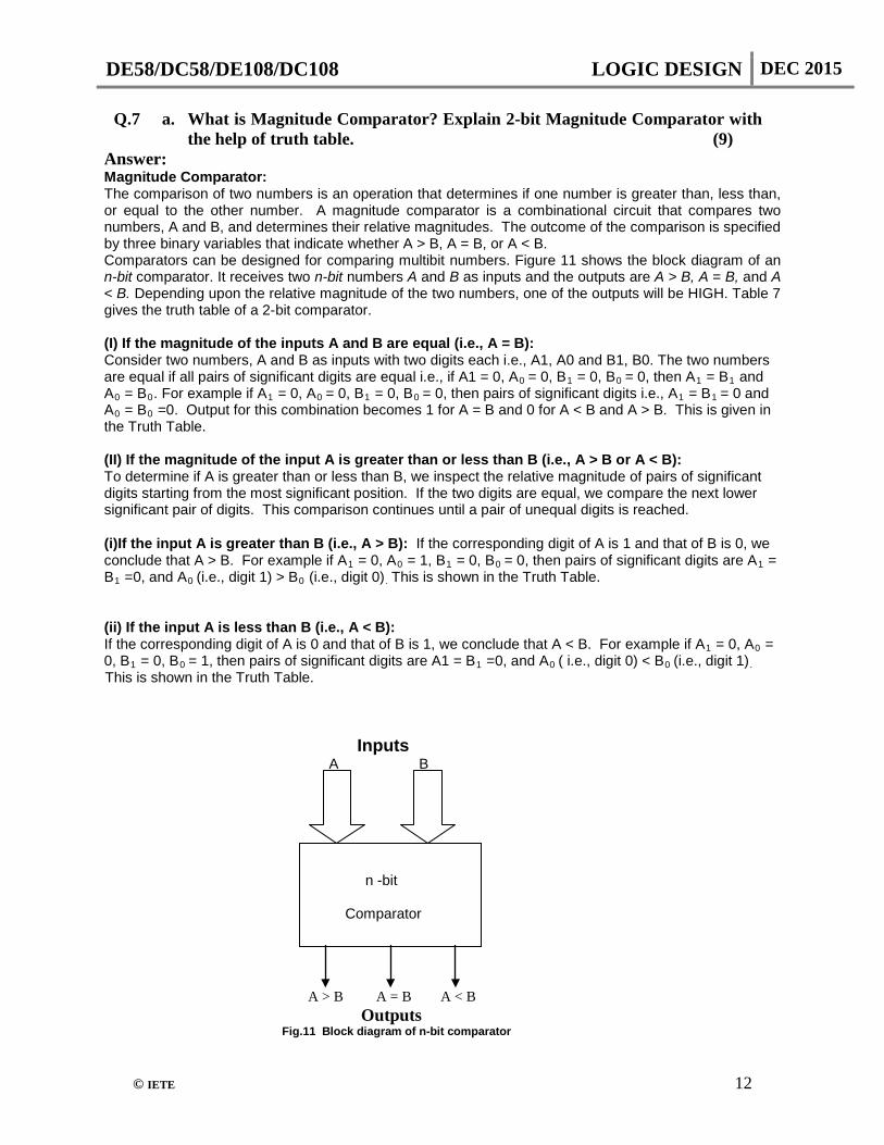
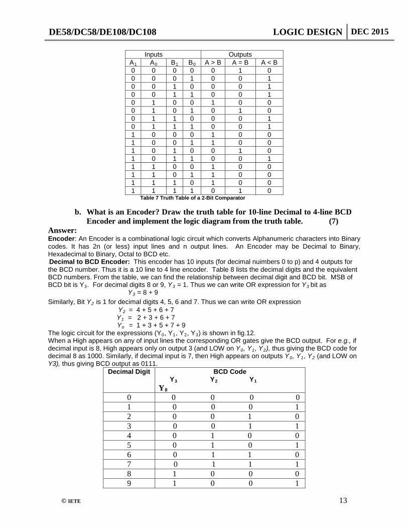
Q.7 a. What is Magnitude Comparator? Explain 2-bit Magnitude Comparator with the help of truth table. (9)
Answer: Magnitude Comparator: The comparison of two numbers is an operation that determines if one number is greater than, less than, or equal to the other number. A magnitude comparator is a combinational circuit that compares two numbers, A and B, and determines their relative magnitudes. The outcome of the comparison is specified by three binary variables that indicate whether A > B, A = B, or A < B. Comparators can be designed for comparing multibit numbers. Figure 11 shows the block diagram of an n-bit comparator. It receives two n-bit numbers A and B as inputs and the outputs are A > B, A = B, and A < B. Depending upon the relative magnitude of the two numbers, one of the outputs will be HIGH. Table 7 gives the truth table of a 2-bit comparator. (I) If the magnitude of the inputs A and B are equal (i.e., A = B): Consider two numbers, A and B as inputs with two digits each i.e., A1, A0 and B1, B0. The two numbers are equal if all pairs of significant digits are equal i.e., if A1 = 0, A0 = 0, B1 = 0, B0 = 0, then A1 = B1 and A0 = B0. For example if A1 = 0, A0 = 0, B1 = 0, B0 = 0, then pairs of significant digits i.e., A1 = B1 = 0 and A0 = B0 =0. Output for this combination becomes 1 for A = B and 0 for A < B and A > B. This is given in the Truth Table. (II) If the magnitude of the input A is greater than or less than B (i.e., A > B or A < B): To determine if A is greater than or less than B, we inspect the relative magnitude of pairs of significant digits starting from the most significant position. If the two digits are equal, we compare the next lower significant pair of digits. This comparison continues until a pair of unequal digits is reached.
(i)If the input A is greater than B (i.e., A > B): If the corresponding digit of A is 1 and that of B is 0, we conclude that A > B. For example if A1 = 0, A0 = 1, B1 = 0, B0 = 0, then pairs of significant digits are A1 = B1 =0, and A0 (i.e., digit 1) > B0 (i.e., digit 0). This is shown in the Truth Table.
(ii) If the input A is less than B (i.e., A < B): If the corresponding digit of A is 0 and that of B is 1, we conclude that A < B. For example if A1 = 0, A0 = 0, B1 = 0, B0 = 1, then pairs of significant digits are A1 = B1 =0, and A0 ( i.e., digit 0) < B0 (i.e., digit 1). This is shown in the Truth Table. Inputs A B n -bit Comparator A > B A = B A < B Outputs Fig.11 Block diagram of n-bit comparator
DE58/DC58/DE108/DC108 LOGIC DESIGN DEC 2015
© IETE 13
Inputs Outputs A1 A0 B1 B0 A > B A = B A < B 0 0 0 0 0 1 0 0 0 0 1 0 0 1 0 0 1 0 0 0 1 0 0 1 1 0 0 1 0 1 0 0 1 0 0 0 1 0 1 0 1 0 0 1 1 0 0 0 1 0 1 1 1 0 0 1 1 0 0 0 1 0 0 1 0 0 1 1 0 0 1 0 1 0 0 1 0 1 0 1 1 0 0 1 1 1 0 0 1 0 0 1 1 0 1 1 0 0 1 1 1 0 1 0 0 1 1 1 1 0 1 0
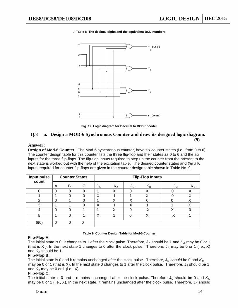
Table 7 Truth Table of a 2-Bit Comparator b. What is an Encoder? Draw the truth table for 10-line Decimal to 4-line BCD
Encoder and implement the logic diagram from the truth table. (7) Answer: Encoder: An Encoder is a combinational logic circuit which converts Alphanumeric characters into Binary codes. It has 2n (or less) input lines and n output lines. An Encoder may be Decimal to Binary, Hexadecimal to Binary, Octal to BCD etc. .Decimal to BCD Encoder: This encoder has 10 inputs (for decimal nuimbers 0 to p) and 4 outputs for the BCD number. Thus it is a 10 line to 4 line encoder. Table 8 lists the decimal digits and the equivalent BCD numbers. From the table, we can find the relationship between decimal digit and BCD bit. MSB of BCD bit is Y3. For decimal digits 8 or 9, Y3 = 1. Thus we can write OR expression for Y3 bit as Y3 = 8 + 9 Similarly, Bit Y2 is 1 for decimal digits 4, 5, 6 and 7. Thus we can write OR expression Y2 = 4 + 5 + 6 + 7 Y1 = 2 + 3 + 6 + 7 Yo = 1 + 3 + 5 + 7 + 9 The logic circuit for the expressions (Y0, Y1, Y2, Y3) is shown in fig.12. When a High appears on any of input lines the corresponding OR gates give the BCD output. For e.g., if decimal input is 8, High appears only on output 3 (and LOW on Y0, Y1, Y2), thus giving the BCD code for decimal 8 as 1000. Similarly, if decimal input is 7, then High appears on outputs Y0, Y1, Y2 (and LOW on Y3), thus giving BCD output as 0111.
Decimal Digit BCD Code Y3 Y2 Y1 Y0
0 0 0 0 0 1 0 0 0 1 2 0 0 1 0 3 0 0 1 1 4 0 1 0 0 5 0 1 0 1 6 0 1 1 0 7 0 1 1 1 8 1 0 0 0 9 1 0 0 1
DE58/DC58/DE108/DC108 LOGIC DESIGN DEC 2015
© IETE 14
. Table 8 The decimal digits and the equivalent BCD numbers
3
2
1
0
Y
Y
Y ( MSB )
Y ( LSB )
98
7
65
4
3
2
1
Fig. 12 Logic diagram for Decimal to BCD Encoder
Q.8 a. Design a MOD-6 Synchronous Counter and draw its designed logic diagram.
(9) Answer: Design of Mod-6 Counter: The Mod-6 synchronous counter, have six counter states (i.e., from 0 to 6). The counter design table for this counter lists the three flip-flop and their states as 0 to 6 and the six inputs for the three flip-flops. The flip-flop inputs required to step up the counter from the present to the next state is worked out with the help of the excitation table. The desired counter states and the J K inputs required for counter flip-flops are given in the counter design table shown in Table No. 9. Input pulse
count Counter States
A B C
Flip-Flop Inputs
JA KA JB KB JC KC 0 0 0 0 1 X 0 X 0 X 1 1 0 0 X 1 1 X 0 X 2 0 1 0 1 X X 0 0 X 3 1 1 0 X 1 X 1 1 X 4 0 0 1 1 X 0 X X 0 5 1 0 1 X 1 0 X X 1
6(0) 0 0 0
Table 9 Counter Design Table for Mod-6 Counter
Flip-Flop A: The initial state is 0. It changes to 1 after the clock pulse. Therefore, JA should be 1 and KA may be 0 or 1 (that is X ). In the next state 1 changes to 0 after the clock pulse. Therefore, JA may be 0 or 1 (i.e., X) and KA should be 1. Flip-Flop B: The initial state is 0 and it remains unchanged after the clock pulse. Therefore, JB should be 0 and KB may be 0 or 1 (that is X). In the next state 0 changes to 1 after the clock pulse. Therefore, JB should be 1 and KB may be 0 or 1 (i.e., X). Flip-Flop C: The initial state is 0 and it remains unchanged after the clock pulse. Therefore JC should be 0 and KC may be 0 or 1 (i.e., X). In the next state, it remains unchanged after the clock pulse. Therefore, JC should
DE58/DC58/DE108/DC108 LOGIC DESIGN DEC 2015
© IETE 15
be 0 and KC may be 0 or 1 (i.e., X).The JK inputs required for this have been determined with the help of the excitation table, shown in Table No.8. The flip-flop input values are entered in Karnaugh maps shown in Fig. 13 ((i), (ii), (iii), (iv), (v), and (vi)) and a boolean expression is found for the inputs to the three flip-flops and then each expression is simplified. As all the counter states have not been utilized, Xs (don't) are entered to denote un-utilized states. The simplified expressions for each input have been shown under each map. Finally, these minimal expressions for the flip-flop inputs are used to draw a logic diagram for the counter shown in fig.14. As before, the JK inputs required for this have been determined with the help of the excitation table, (Table 9.). These input values are entered in Karnaugh maps Fig. 13 [i to vi] and a boolean expression is found for the inputs to the three flip-flops and then each expression is simplified. Xs have been entered in those counter states which have not been utilized. The simplified expressions for each input have been shown under each map and finally a logic diagram based on these expressions is drawn and is shown in Fig. 13 [i to vi].
B C B C BC B C B C B C B C B C
A
1
1
X
1
A
X
X
X
X
A
X
X
X
X
A
1
1
X
1
Map for JA Map for KA JA = 1 KA = 1 Fig.(i) Fig.(ii)
B C B C BC B C B C B C B C B C A
0
0
X
X
A
X
X
X
0
A
1
0
X
X
A
X
X
X
1
Map for JB Map for KB JB = A C KB = A Fig.(iii) Fig.(iv)
B C B C BC B C B C B C B C B C A
0
X
X
0
A
X
0
X
X
A
0
X
X
1
A
X
1
X
X
Map for JC Map for KC JC = AB KC = A Fig.(v) Fig.(vi)
Fig. 13 Karnaugh Maps for JA,KA,JB,KB,JC,KC
DE58/DC58/DE108/DC108 LOGIC DESIGN DEC 2015
© IETE 16
J
K
A
A
A
FFA
CLOCKPULSES
_A
J
K
C
C
C
FFC
_C
J
K
B
B
B
FFB
_B
1
1
AB
C
Fig. 14 Logic Diagram for MOD-6 Synchronous Counter
b. Draw the logic diagram for 4-bit Serial Input and Serial Output Shift Register and explain its working with timing waveform. (7)
Answer: SERIAL IN - SERIAL OUT SHIFT REGISTER: Fig. 15 shows a 4 bit serial in - serial out shift register consisting of four D flip flops FF0, FF1, FF2 and
FF3. As shown it is a positive edge triggered device. The working of this register for the data 1010 is given in the following steps.
D Q D QD Q D Q0 0 1 1 2 2 3 3
FF FF FF FF1 2 30
DATA IN
CLOCK
_Q 3
Fig. 15 Logic Diagram of 4-bit Serial In – Serial Out Shift Register
1 2 3 4
Q
Q
Q
Q
0
1
2
3
CLK
DATA1 0 1 0
Fig.16 Output Waveforms of 4-bit Serial-in Serial-out Register
DE58/DC58/DE108/DC108 LOGIC DESIGN DEC 2015
© IETE 17
1. Bit 0 is entered into data input line. D0 = 0, first clock pulse is applied, FF0 is reset and stores 0. 2. Next bit 1 is entered. Q0 = 0, since Q0 is connected to D1, D1 becomes 0. 3. Second clock pulse is applied, the 1 on the input line is shifted into FF0 because FF0 sets. The 0
which was stored in FF0 is shifted into FF1. 4. Next bit 0 is entered and third clock pulse applied. 0 is entered into FF0, 1 stored in FF0 is shifted
to FF1 and 0 stored in FF1 is shifted to FF2. 5. Last bit 1 is entered and 4th clock pulse applied. 1 is entered into FF0, 0 stored in FF0 is shifted
to FF1, 1 stored in FF1 is shifted to FF2 and 0 stored in FF2 is shifted to FF3. This completes the serial entry of 4 bit data into the register. Now the LSB 0 is on the output Q3.
6. Clock pulse 5 is applied. LSB 0 is shifted out. The next bit 1 appears on Q3 output. 7. Clock pulse 6 is applied. The 1 on Q3 is shifted out and 0 appears on Q3 output. 8. Clock pulse 7 is applied. 0 on Q3 is shifted out. Now 1 appears on Q3 output. 9. Clock pulse 8 is applied. 1 on Q3 is shifted out. 10. When the bits are being shifted out (on CLK pulse 5 to 8) more data bits can be entered in.
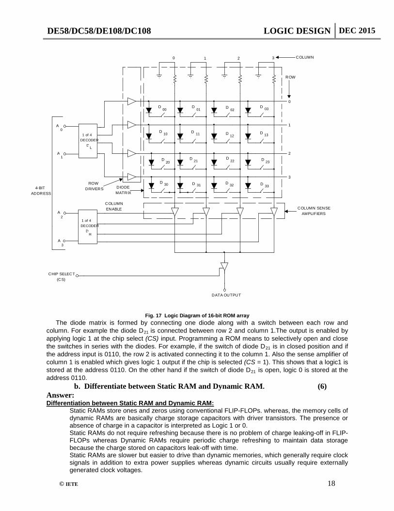
Fig. 16 shows the output waveforms of 4-bit Serial-in Serial-out Register. Q.9 a. Draw and explain the architecture of 16 X 8 ROM. (10) Answer:
Architecture of 16 X 8 ROM: A read-only memory is an array of selectively open and closed unidirectional contacts .A 16 X 8 ROM array is shown in Fig. 17. To select any one of the 16 bits, a 4-bit address (A3, A2, A1, A0) is required. The lower order two bits (A1, A0) are decoded by the decoder DL which selects one of the four rows, whereas the higher order two bits (A3, A2) are decoded by the decoder DH which activates one of the four column sense amplifiers.
DE58/DC58/DE108/DC108 LOGIC DESIGN DEC 2015
© IETE 18
1 of 4DECODER D
1 of 4 DECODER D
L
H
CHIP SELECT (CS)
DATA OUTPUT
0
1
2
3
0 1 2 3
COLUMN SENSE AMPLIFIERS
A
A
A
A
0
1
2
3
ROW
COLUMN
COLUMN ENABLE
DIODEMATRIX
ROWDRIVERS 4-BIT
ADDRESS
D
D
D
D
D
D
D
D D
DD
D
DD D
D
00 01
10 11
20
30
21
03
13
02
12
22
32
23
3331
Fig. 17 Logic Diagram of 16-bit ROM array The diode matrix is formed by connecting one diode along with a switch between each row and
column. For example the diode D21 is connected between row 2 and column 1.The output is enabled by applying logic 1 at the chip select (CS) input. Programming a ROM means to selectively open and close the switches in series with the diodes. For example, if the switch of diode D21 is in closed position and if the address input is 0110, the row 2 is activated connecting it to the column 1. Also the sense amplifier of column 1 is enabled which gives logic 1 output if the chip is selected (CS = 1). This shows that a logic1 is stored at the address 0110. On the other hand if the switch of diode D21 is open, logic 0 is stored at the address 0110. b. Differentiate between Static RAM and Dynamic RAM. (6) Answer: Differentiation between Static RAM and Dynamic RAM:
Static RAMs store ones and zeros using conventional FLIP-FLOPs. whereas, the memory cells of dynamic RAMs are basically charge storage capacitors with driver transistors. The presence or absence of charge in a capacitor is interpreted as Logic 1 or 0. Static RAMs do not require refreshing because there is no problem of charge leaking-off in FLIP-FLOPs whereas Dynamic RAMs require periodic charge refreshing to maintain data storage because the charge stored on capacitors leak-off with time. Static RAMs are slower but easier to drive than dynamic memories, which generally require clock signals in addition to extra power supplies whereas dynamic circuits usually require externally generated clock voltages.

DE58/DC58/DE108/DC108 LOGIC DESIGN DEC 2015
© IETE 19
Advantages of Static RAMs over Dynamic RAMs: (i)Higher speed of operation (faster) i.e, lower access –time.
(ii)Does not require refreshing. Advantages of Static RAMs over Dynamic RAMs:
(i)Higher number of bits storage on a given silicon chip area. i.e., Higher packaging density. (ii)Lower power consumption.

DE58/DC58/DE108/DC108 LOGIC DESIGN DEC 2015
© IETE 20
TEXT BOOK
I. Digital Systems – Principles and Applications, Ronald J Tocci, Neal S. Wildmer, Gregory L. Moss, Ninth Edition, Pearson Education, 2008