Embed Size (px)
Citation preview

Q0

The work reported in this document was peroed a Lino Labouatorya ceofor research operated by Massachusetts istitute of Technolo. ThiU work wosponsored by the Defense Advanced Re r Pojects Agency under Air ForceContract F12S84J0-C.00 (ARPA Order 3797).
The views and conclusions contained in this document are those of the contractor andshould not be interpreted as necessarily representing the offical policie eitherexpressed or implied, of the United States Government.
The Public Affairs Office has reviewed this report, and it isreleasable to the National Technical Information Service,where it will be available to the general public, includingforeign nationals.
¶"[is technical report has been reviewed and is approved for publication,
FOR THE COMMANDER
Thomas J. Alpert, Major, USAFChief, ESD Lincoln Laboratory Project Office
I
Non-Lincoln Recipients
PLEASE DO NOT RETURNPermission is given to destroy this documentwhen it is no longer needed.

% 7.
MASSACHUSETTS INSTITUTE OF TECHNOLOGY
LINCOLN LABORATORY
RESTRUCTURABLE VLSI PROGRAM
SEMIANNUAL TECHNICAL SUMMARY REPORT
TO THE
DEFENSE ADVANCED RESEARCH PROJECTS AGENCY
1I APRIL - 30 SEPTEMBER 1992
ISSUED 12 JANUARY 1983
Approved for public release; distribution unlimited. *E T E
MAR 3 11983
Aq
LEXINGTON MASSACHTUSETTS
All~"i DTCrpol-.;
iAoe ns will be In buaon limtdwhiteo
S.I.-.-- -

I,.
ABSITRACT
This report describes work on the Restructurable
VLSI Research Progre. sppnrsored by the Information
Processing Techniques Office of the Defense Advanced
Research Projects Agency during the semiannual period
1 April through 30 September: 1982. C-
STA-
Z~ Da
tiii
.y

TABLE OF CONTENTS
Abstract jiii
I. PROGRAM OVERVIEW AND SUMMARY
A. Overview !B. Summary of Progress 2
1. Design Aids for RVLSI 32. RVLSI Technology 33. Testing 44. Applications 4
II. DESIGN AIDS FOR RVLSI 7
A. MACPITTS 7B. Mask Artwork Analysis Tools 17C. LBS - The Lincoln Boolean Synthesizer 18
1. Introduction 182. Chronology 193. Weinberger Arrays 20 ¶4. Miscellaneous Layout Features 245. Software Engineering Issues 25
6. LBS User Level 277. Summary 33 3
III. RVLSI TECHNOLOGY 35
IV. TESTING 43
V. APPLICATIONS 47
A. Digital Integrator 471. Phase 0 Integrator 472. Phase 1 Wafer 51
B. DSP Chip Designs 521. Systolic Correlators 522. Digital AGC Controller 53
C. Vector Digital Signal Processor (VDSP) 531. Introduction 532. Vector Processor 553. Program Complexity 554. Hardware Architectures and Chaining 575. Breakdown of the Instruction Architecture 586. Full Dyadic 60
References 62
V

r. . . . . . .- - - - ' -, -, - . - • o =
"RESTRUCTURABLd VLSI PROGRAM
.. PROGRAM OVERVIEW AND SUMMARY
"A. OVERVIEW
The main objective of the Lincoln Restructurable VLSI Progrw, (RVLSI) is
to develop methodologies and architectures for implementing wafer-scale
systems with complexities approaching a million gates. In our approach, we
envisage a modular style of architecture comprising an array of cells
embedded in a regilar interconnection matrix. Ideally, the cells should
consist of only a few basic types. The interconnection matrix is a fixed
pattern of metal lines augmented by a complement of pigratmable switches or
links. Conceptually, the links could be either volati'e or nonvolatile.
They could be of an electronic nature such as a transiator switch, or could
be permanently programmed through some mechanism such as a laser. The RVLSI
Program is currently focusing on laser-formed interconnect.
The link concept offers the potential for a highly flexible,
restructurable type of interconnect technology that could be exploited in a
variety of ways. For example, logical cells or subsystems found to be
faulty at wafer-probe time could be permanently excised from the rest of the
wafer. The flexible interconnect could also be used to *jump around' faulty
logic and tie in redundant cells judiciously scattered around the wafer for
chis purpose. slo, the interconnect could be tailored to a specific
application in or •e .inimize electrical degradations and performance
penalties caused by unused wiring.
Further, the testing of a particular logical subsystem buried deep
within a complex wafer-scale system poses a very difficult problem. A
pruperly designed restructurable interconnect matrix could be temporarily
*4 configured to render internal cells both controllable and observable from
the wafer ptriphery. In this way, each component cell or a tractable cluster
of cells could be tested in straightforward manner using standard techniques.
i1
F.

With an electronic linking mechanism it is possible to think in terms of
a dynamically reconfigurable system. auch a feature could be used to alterthe fLnctional mode of a system sobject to changes in the operating
scenario, or it could be used to support somb degree of fault tolerance ifthe system architecture was suitably designed.
Several major areas of research have been identified in the context of
the RVLSI concept:
(1) System architectures and partitionings for whole-wafer
implementations.
.(2) Placement and routing strategies for optimal utilization
of redundant resources and efficient interconnect.
(3) Assignment and linking algorithms to exploit redundancy
and flexible interconnect.
(4) Methods for expediting cell design with emphasis on
functional level descriptions, enhanced testability, and
fault tolerance.
(5) Methods for testing complex, multiple-cell, whole-wafer
systems.
Complementary work on the development of various link and interconnect
technologies aa well a, fabrication/procensing technology is being supported
by the Lincoln Air Force Line Program, and results are reported unier the
Lincoln Laboratory Advanced Electronic Technology Quarterly Technical
Summary.
B. SUMMARY OF PROGRESS
Work for this period is reported und r four headings: Design Aids for
RVLSI (Sec. II), RVLSI Technology (See. III), Testing (Sec. TV), and
Applications (Sec. V). The following paragraphs summarize progress to date.
2

I. Design Aids for RVL81
An initial version of the MACPITTS silicon compiler has been made
available for internal use. This version of the compiler features a variety
of improvements in the specific areas of memory/run-time efficiency, layout
area efficiency, and electrical uerrormance. These improvements involved a
rewrite of the L5 geometric layout language, the incorporation of packing
and ordering algorithms to reduce the area requirements of the Weinberger
array and the data path internal bus complex, and the judicious use of metal
and polysilicon for long interconnects. To improve user friendliness, an
interpretive type simulator has been added to aid in design validation and a
user manual has been prepared. Two modest test circuits have been processed
through MOSIS at 5 uan and found to function properly. Maximum clock rates
weee observed to be in the I- to 2-M4Hz range indicating that further
improvements in circuit performance are warranted.
Versions of the Lincoln mask design rule checker (H4DRC) are now
operational for 4- and 5-M MOSIS NMOS with buried conLacts as well as
Lincoln and M4OSIS/JPL CMOS. Designs comprising as much as 80,000 rectangles
have been successfull7 checked requiring about 80 CPU minutes. A CHOS node
extractor is atso currently operational for both Lincoln and MDSIS processes
as well as a modified form of the M.I.T. switch-level simuletor.
A CMOS-oriented automatic synthesis tool for implementing Boolean logic
has been developed. This system, called the Lincoln Boolean Synthesizer
(LBS), ia based on a Weinberger array style of gate layout. A simulator also
has been written to expedite design verification. Sieveral test designs were
submitted on the July CMOS run.
2. RVLSI Technology
A lateral type of laser programmable link has been evaluated which is
compatible with the 1-level-metal MOSIS processing environment. Polyimide is
used as the link insulator material. This substance, when volatized by a
laser pulse, is converted to a nearly purely carbonaceous conductive residie.
3

- - , - - . . - G " . ' ,- • •' • . . ."' t • * ' ,• '- •;'; • ••, • ,'
K Sxtevisive analyeis of test data indic;ates resistances typically beaween 1 and
2 kn. An uncommitted, laser progrmmable 256-gate Weinberger array tas been
submittea to HOSIS as a test vehicle. The polyinide layer wiil be added at
"-" Lincoln. A 4-bit ALU similar to the classical 74!81 has been laid out on the
gate array and will constitute the first feasibility demonstration.
3. Testing
A compact, inexpensive, easily replicated circuit tester has been
defined based on the 4-bit casuadable tester-on-chip (TOC) slice. The tester
consists of a UART, an address generator complex, and any number of 4-bit-
widt modular circuit test interface boards. The board modules consist of a
4K test vector memory complex and a TOC chip. The address generator
involves a second custom circuit specialized for this purpose. The designs
of the TOC and address generator chips are well under way using the MACPITTS
silicon compiler. A design goal is maximum compatibility of this system with
the Stanford IC test language.
4. Applications
A Phase 0 (limited capability) digital integrator wafee was
successfully linked thereby demonstrating the basic viability Gf the laser-
based restructuring concept from start to finish. A 5 x 7 array of 4-bit
counter cells was probed and 21 wree found functional. Three percent of the
interconnecL was discovered to be faulty. A somewhat specinlized RVLSI CAD
tool package (LSH) was used for logical/physical device specification, test
data analysis, and assignment/linking. This system was coupled with the
restructurable wafer editor software (RWED) which automatically made the
required laser zaps and cuts te assemble a wcrking 4 x 4 array of cells. The
ability to check interconnect and test-while-zap proved essential.
The full 3-in. wafer design for the Phase I (full capability) digital
integrator has been completed. Processing through the third mask level has
been completed. The design includes 200-percent cell redundency and
4
6.

100-percent interconnect redundancy. The link population has been reduced to
about 15-percent of the maximum possible, A clock distribution system has
been designed and verified through SPICS simulation to be capable of
eupporting 25-101s operation. The wafer will ba triuad to 2.25 in. 2 for
final packaging.
An architectural study has been initiated investigating vector-oriented
computing structures for digital signal processing in terms of their
throughput capability, complexity, programmability, and menability to VLSI
implementation. A programmer's model has been developed based on an APL-likelanguage. Novel concepts under investigation Include the explicit hardware
chaining of function modules to reduce memory access overhead. Variouscrossbar switch structures are being examined as potential candidates for
supporting tiae chaining feature. Initial indications are that a bit serial
crossbar approach represents the only practical means of implementing a
switch of the dimensionality needed and analyses of the performance
degradations introduced by this technique are under way using selected signal
processing benchmarks.
U'
5
ra

II. DESIGH AIDS FOR RYLS1
A. MACP1ITTS
Durin.g the second half of FY 82 the initial HMI10 version of the HACPITTS
system was finished and installed for general internal use. Many changes and
enhancements were required before the compiler could be made viailable.
These improve.aents fell into several ctcegories. One task was to make the
compiler accommodate large designs more gracefully. This involved developing
new algorithms or implementation strategies to improve speed and memory
efficiency. Another task was to enhance silicon area efficiency. The
current main NMOS fabrication source is the DARPA/MOSIS silicon foundry. For
mask fabrication related reasons, user chip sizes are restricted to about
7 by 9 mm. M4ost of the larger designs generated thus far have tended to
exceed that area. Considerable effort has been expended in reducing the sise
of these designs by creating denser layouts, using better routing and packing
algorithms and exploiting finer minimum feature sizes. Electrical
performance is also an area of continuing concern and will involve furthercircuit design improvements. Finally, since MACPITTS row has a smaller usercommunity, some effort has been devoted to providing a design validation
mechanism through simulation.
The MACPITTS system structure has changed since the last Semiannual1
Technical Summary. It is depicted in Fig. I, where the rectangles are major
system components and the circles represent data in files or intermediate
data structures. One notable change is that state sequencers are no longer
laid out as a separate entity. Since a sequencer is simply a register or a
group of registers and an incrementer, it can be efficiently merged into the
data path and control. This was done primarily to simplify the chip layout
and did not affect the size of a design by more than ±5 percent. Another
change is that there is no longer a simulator as such. During development of
the MACPITTS system, a simulator was required to help debug the compiler. It
operated from the intermediate object code and would point to problems if the
÷'7
S• : . . .. - _ _ _ • ,. • • . . . .• •. .. •. __ _• • . . .• . . . . -.7

SOURCE
USER
nEFAULTLIBRAR(Y PIREPASS INTERPRETER
TECHNOLOGY-INDEPENDENT FEATURE EXTRACTION
PATA CONTROL FLAGS PINS
PATH
LAYOUT LAYOUT LAYOUT LAYOUT
-- PLACEMENT AND ROUTING
C
Fig. 1. MACPITTS structure.
8
t'J

object code was incorrect. Now that the compiler design is relatively
stable, use of simulation at this level has been discontinued. Instead, in
order for the designer to check the correctness of his program, a MACPITTS
source code interpreter has been written. This interpreter is screen
oriented and user friendly. The setup time is also faster than the old
simulator, since it operates from the source code instead of the intermediate
code. It has been tested on all the sample designs and found to be useful.
However, the interpretation speed on large designs is slow and could be
"improved.
In any compiler, speed and memory consumption are important
considerations. In the case of MACPITTS, the compiler worked well for small
designs but required an inordinate amount of memory when compiling larger
designs. This was due to the fact that the internal representation of the
layout was kept entirely in virtual memory as the circuit was being compiled.
Using the LISP list representation for rectangles, each rectangle consumes
approximately 6- bytes of memory. With perhaps I Mbyte of memory left over
afte-.r loading the MACPITTS compiler, etc., there is room for only 16K
rectangles. Large designs can easily surpass this limit.
The solution involved a rewrite of the L5 layout language component to
allow off-loading of completed sections of the layout into a disk file. The
major change to L5 entailed the creation of a "defsymbol" macro. Defsymbol
is similar to a normal function definition except that it is intended for use
when the function is totally applicative and returns a layout item. When a
routine which has been defined using defsymbol io called, L5 first checks to
see whether that routine has been called before with the same arguments. If
so, it returns immediately with a CIF symbol call to that symbol which has
already been defined. If not, it executes the body of the function, dumps
the layout to file as a CIF symbol, remembers the CIF symbol number and
parameters to the defsymbol call, and returns a CIF symbol call to the newly
created symbol. This has two benefits. First, the amount of memory required
is decreased drastically. Large designs can be compiled in as little as 500K
of virtual memory. Second, the compilation time is decreased since the
unnecessary recomputation of layout for routines which are called
9

repetitively has been removed. Many of the layout routines in the MACPITTS
compiler needed modification to make use of defsymbol.
During the last reporting period some major enhancements were made to
the layout portions of the compiler as well. These enhancements, detailed
below, comprised primarily layout optimizations which were required to enable
fabrication of larger MACPITTS designs.(1) The Weinberger array layout was changed to eliminate
the long ground lines. The length of the ground
lines would have caused larger designs to fail.
This layout is also four times as compact as the oldlayout.
(2) The ordering routines that increase the bus density
in both the data path and control have been
upgraded. The speed of these heuristics could be
improved further.
(3) Signal lines were routed in polysilicon instead of
diffusion. This allowed closer spacing of signal
lines and should improve performance.
Another way to shrink the size of the design is by using a finer
geometry process, such as 3 or 4 Um. This is accomplished by a simple
variable change in most of the MACPITTS system. However, the present I/O pad
designs are not lambda scalable. Therefore, for each feature size, a new set
of pads is required. A general mechanism for including new sets of pads was
written and 4-um pads were adapted from the MOSIS CIF library.
After any substantial change in the compiler, it is exercised by
attempting to compile the extensive set of snmDte programs which have
accumulated during the design of MACPITTS. Short descriptions of some of
these programs follow:
COUNTER is a 4-bit resettable counter which is
programmable to count to any number between one and
sixteen.
10

SHIFTER is a 4-bit universal shift register which
can be loaded and read from a tri-state bi-directional
bus and can shift both left and right.
ADDRESSER is a device which is meant to attach to a
microprocessor bus and provide chip select signals for
devices attached to that bus. The device is programmed
with a match address, match mask, and chip select
" polarity. Whenever it senses an address on the bus
matching the match address under the match mask, a chip
select pin is asserted according to the selected
polarity.
TAXI is a taxicab meter controller.
TOC is a 4-bit slice of an extendable test
vector applicator.
FRISC is a 16-bit stack-oriented microprocessor.
CORR is a correlator base on an in-house systolic
architecture.
APU is part of a 32-bit floating-point processor
chip.
ADD-SUB is an 8-bit adder subtracter circuit
useful in discrete cosine transform applications.
One part of the compiler checkout process involves fabricating MACPITTS
generated designs. Three designs, the COUNTER, SHIFTER, and ADD-SUB were
fabricated through MOSIS in the third quarter of FY 82. COUNTER and SHIFTER
were tested on a simple test setup and found to work functionally. They have
also been tented on the Tektronix 3260 tester. The maximum obtainable clock
rate was I MHz for the COUNTER and 2 MHz for the SHIFTER. These results were
somewhat disappointing and have prompted more concern regarding the circuit
performance of MACPITTS generated chips. Microphotographs for both circuits
appear in Figs. 2 and 3. It is important to note that, during the compiler
development, all the standard VLSI CAD tools were used to check out the
' 11

Fig. 2. Photomicrnorapli of shifter design.
13

.01 -w- 1 ap
Fig. 3.Photouiicrogrdph of counter design.
15

automatically generated designs. As the compiler gets wvre uses, the need
for these other tools for checkout should diminish, sirce the end product
will be correct by construction.
Additionally, a user's manual has been written and internal laboratory
usage is being encouraged. User feedback will be helpful in focusing irn on
further improvements in the definition language and target architecture
capabilities. Due to the suboptimal circuit speed, another development focus
will bi on improvement of the electrical performance of generated designs.
In particular, greater attention should be paid to the dividing of long
signal lines emanating from the control section. Also, the clock
distribution and organelles should be designed with greater care. Note that
these improvements do not drastically change the intrinsic operating concept
or internal structure of the MACPITTS system, but are more properly
characterized as gradual refinements. It is expected that several larger
designs will be submitted for fabrication in the near future. Some of these
designs will be drawn from the candidates described above, in particular TOC.
Others will be produced by the internal user community as they become
familiar with the capabilities of the MACPITTS system.
M. ASK ARTWORK ANALYSIS TOOLS
This past six months marked a period of intensivi effort in the area of2
application for the MDRC system. We now have fully operational geometric
design rule checking for the following technologies:
(1) 4OSIS NMOS 5-Pm rules (with buried contacts).
(2) MOSIS NMOS 4-pm rules (with buried contacts).
(3) M10SIS JPL CMOS.
(4) LL CMOS.We have checked artwork from a variety of sources, ranging from CALMA
custom layouts to MACPITTS compiled designs. We have produced a variety of
outputs including text file listing of errors, stipple plots, and magnetic
tape suitable for reading on the CALMA system. We have been able to check
17
L

all design rules, and generate no false alarms. The largest designs chz.ked
to date have been the MACPITTS compiled TOC (cf. Sec. 111-D) and FRISC chips.
These chips comprise approximately 80,000 rectangles each and were handled
easily by the system. Checking time was apnroximately 80 CPU minutes.
Because of the layout method, these chips represent close to a worst-case
situation for the checker. Indications are that run-time can be improved for
large chips.
The MDRC system was expanded to provide a node extraction capability.
The designer specifies a set of node extraction rules for a particular
process, in manner similar to the way geometric design rules are specified.
These rules are then translated into zhe appropriate low-level Mask Data
Processing (MDP) primitives which, along with the artwork, drive the MuP
program. The primary, output from this node extraction is a transistor
network file, suitable for switch-level simulation. We have node extracted
and switch-level simulated MOSIS NMOS, MOSIS CMOS, and Lincoln CMOS desig'as
(including two-level metal).
The artwork analysis tools described above have proven invaluable in
expediting CALMA custom layouts such as the Phase 0 integrator cell
(Sec. Ill-A), and debugging and verifying circuit sythesis tools such as
MACPITTS and LBS (Secs. I-A, I-C).
C. LBS - THE LINCOLN BOOLEAN SYNTHESIZER
I. Introduction
Because of the pace of fabrication improvements, a real VLSI design,
especially in its layout phase, is attempting to track a fast-moving target.
it is not unusual for a large design to be partially complete when design
"rules and fabrication parameters are changed, necessitating substantial
rework or use of the inferior process. In the production phase of any
moderately successful design even more fabricatIon improvements can be
expected, and the decision to redesign or not is similarly painful.
18
- - - - - - --

The lambda-based, scaled design style promulgated by Ne*d and Convey 3 is
one method of incorporating fabrication improvements without redoing the IC
layout. Using this method, reduction in size of one feature cannot be
utilized until all fabrication features can be reduced by the same amount.
This lambda-based scaling design style is analogous to instruction set upward
compatibility in a family of computer processors.
The LBS style of IC design allows more flexible incorporation of
fabrication improvements, also without redoing ':he desigi specification. The
LBS upward compatibility is based on an analogy with a high-level language
compiler. The user specifies design at the logic level, which is technology
independent. The lowest level layout routines of the compiler are rewritten
f~r each improvement in fabrication capability. Designs take advantage of
improved fabrication capabilities by being recompiled to the new technology.
A critical question is: Can a compiler such as LBS be retargeted to new
fabrication capabilities as fast, or faster than those new capabilities can
be physically instituted? This question can now be tentatively answered in
the affirmative. LBS was implemented for the MOSIS bulk CM1DS process in the
two months between the announcement of design rules and the close of the
first fabrication run. A minor design rule change was brought to our
attention two weeks before the close and was 4iccessfully incorporated in
LBS. Seven small-to-medium scale designs which had been created in the LBS
format were quickly retargeted to the new rules.
2. Chronology
The imminent availability of a CMOS process for the DARPA VLSI community
was announced in June 1982. Design rules also were released at this time and
the closing date for the first run was set for early July. Lincoln
Laboratory decided to participate by implementing a Boolean expression
synthesizer for CMOS and using it to produce several designs. We already had
experience implementing a BooleAn logic synthesizer as part of the MACPITTS4
silicon compiler effort.
19

A short investigation determined the suitability of Weinberger arrays
for CaDS. Weinberger arrays are the l(ACPITTS mechanism for implementing
Boolean logic. In 0OS they are easily laid out and piaked, and signals
between gates are eouted without difficulty. Several of the advantages of
NMDS Weinberger arrays are compromised if a straightforward implementation in
CMDS is attempted. However, we were able to demonstrate compiler-level
transformation for problem cases which resulted in simple and alectrically
acceptable Weinberger array layouts.
The task of comnleting LBS was then split into two major parts. The
first part consisted of generating tha array layout from a topclogiial
* intermediate format. The second part consisted of determining the format of
* LBS user specifications and generating the intermediate format from thim.
Pad layout, power, ground, and signal routing were other tasks which needed
to be completed before a complete chip could be designed.
Finally, the Lincoln "technology independent" rules checker and node
extractor had to be "personalised" for the MLSIS CODS design rules. As it
happeaed, the NOSIS CMOS run was not closed to designs until late July.
Several designs were coded in LBS including a 4-bit ALU, several master-
slave static flip-.lops, and in osnibus of adders, half.adders, and random
logic. Also, an LBS simolPtor va% ccn.structed which opetates frcm the
topological intermediate (ormat.
Two weeks before zhe close, we discovered that we were using an early
(and hence in.;orrect) set of design rules. Apparently others had done the
same, since we were notified of this by MOSIS before we had submitted any
designs. The layout rourii'es and rules checker and node extractor technology
personalizations were modified, 6nJ the designs recompiled and rechecked in
time.
3. Weinberger Arrays
5Weinberge- arrays are the ?4ACPII'TS method of implementing Boolean
logic. Interesting algorithms were and are still being developed for
20
Z1
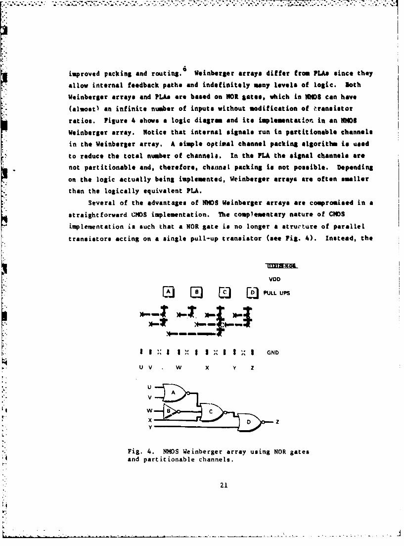
improved packing and routing.* Weinberger arrays differ from PLAs since they
allow internal feedback paths and indefinitely many levels of logic. both
Weinberger arrays and PLA& are based on NOR gates, which in IND8 can have
(almost) an infinite number of inputs without modification of ýransostor
ratios. Figure 4 shows a logic diagram and its implementatiorn in an N368
Weinberger array. Notice that internal signals run tn partitionable channels
in the Weinberger array. A simple optival channel packing algorithm is used
to reduce the total number of channels. In the PLA the signal channels are
- .not partitionable and, therefore, channal packing is not possible. Depending
on the logic actually being implemented, Weinberger arrays are often smaller
than the logically equivalent PLA.
Several of the advantages of NM8 Weinberger arrays are compromised in a
straightforward CMOS implementation. The complementary nature of CHOS
implementation is such that a NOR gate is no longer a structure of parallel
transistors acting on a single pull-up transistor (see Fig. 4). Instead, the
VDD
E]L~] ~] [~PULL UPS
l : I '" l l ( I II .. I ,
UV . W x Y z
A.A
w B C
Fig. 4. NMOS Weinberger array using NOR gatesand partitionable channels.
21

pull-up transistor is replaced by a series structmre of P-channel
transistors. This series structure means that a CNDB A)R gate, with a fixed
transistor width-to-length ratio, cannot tolerate a largt, variation in the
number of inputs. Modifying the width-to-length ratios of the gates
depending on the number of inputs makes the array layout considerably more
difficult. No other gate type, such as HAND or AID-OR-invert has the desired
ratio independence either.
The ratio and other problem were finessed by demonstrating that the
compiler could transform any problea specification into one utilizing only
fixed-ratio NOR gates. For example, a gate with too many inputs can be
partitioned into smaller gates, and followed by some combining logic
- (Fig. 5). Natu,'ally, this may increase the number of levels of logic in the
* critical path and hence decrease the performance of the circuit. However,
the compiler can often be much smarter and transform the initial
specification, rather than the intermediate NOR gate expression. Also, it is
not clear to what extent a single large gate, even when optimally sized, willbe faster than three levels of small gates when placed into a complete
circuit.
1 20829-N ]
-e
Fig. 5. NOR gate partitioning.
22
L

On the other side of the coin, a Weinberger array layout can also reduce
some CHOS electrical problems. The CMOS array can be organised so as to
.equire a single P-tub. The interface between tub and substrate areas is of
intense concern. Diffusion conductors which can be used within each area
cannot cross the boundary, thus reducing the connectivity. The boundary also
form a gap in which no active devices can be placed, reducing effective
area. Of most serious concern, it is at the interface where CMOS latch-up
takes place aud where, in turn, preventive steps must be taken. Because of
this, lees restrictive methodologies, such as STICK (Ref. 7) and SLAP
(Ref. 8), may noc provide advantages commensurate with their added
implementation complexity.
Other researchers are implementing AND-OR-invert logic in a Weinberger9array style. Comparison of results in NIES, however, showed that an AND-OR-
invert implementation of a logic function did not have an appreciable area
advantage over a NOR implementation of the same function. While there may 1 e
some advantage in speed using AND-OR-invert gates, we decided to use only NOR
gates for simplicity in implementation and retargetability.
With the decision to compile LBS to a CMOS Weinberger array, several
other layout decisions were made. It was decided that each signal lino
between gates would run both in the substrate and the P-tub. This was
combined with a rough gate layout which allowed not only an input at every
signal channel but an output from the gate into any channel as well (Fig. 6).
This unrestricted output is freely available in NMOS because .jf the parallel
structure of the NOR gate. It is also available in the CHOS P-tub. However,
in the substrate, the NOR gate's serial structure restricts the output
placement. Additional conductors must therefore be added to the layout in
the substrate.
Many SPICE simulations were done to determine the appropriate transistor
ratios, their implied input limit per gate, and the sensitivity of these to
reasonable modification of fabrication parameters. The N-channel transistors
are 2 X long and 4 A wide. The P-channel transistors are 2 X long and 10 X
wide. Dimensions are balanced for a carrier mobility ratio of 3:1 and for
23

I X CONTACT CUT- -I * P-CHANNEL
P-TUB L I I 1 -1 J TRANSISTOR
U V W X Y
Fig. 6. CMOS Weinberger array.
proidr operation of a 4-input NOR gate driving a fanout of 4. Gates ranging
in complexity from inverters to 6 inputs work reasonably well.
The use of NOR gates was considered. Because the mobility is less for
P-channel transistors they must be made wider. To then place thems in series(as in NOR gates) appears wasteful. By using NAND gates instead, the P-
channel transistors would be placed in parallel and the N-channel transistors
in series. In the actual layout, however, the parallel "ladder" structure
with the narrow gates is well matched to the serial structure of wider gates.
4. Miscellaneous Layout Features
Two layout measures have been taken to prevent latch-up. First, the
power and ground busses run between the P-tub and the active N-substrate
region. Secondly, the P-tub is "tacked" to ground at many points around its
perimeter. Likewise, the substrate is connected to Vdd at points around its
24

perimeter. Although these are elementary measures, they have proved
effective for Lincoln Laboratory's CMOS gate-array designs. As other
measures are discovered, we believe it will be more reasonable to embody this
expertise in the program than to expect every designer to iicorporate all theG
latest knowledge.
Simple input and output pads were designed. Since the LBS language does
not support tri-state signals, there was no neP4 to design tri-state pads.
The signal interconnect between the Weinberger array and the input and
output pads was simplified by constraining the input pads to be on one side
and the output pads on the opposite side. Power and ground pads were placed
on the other two sides. The signals were then routed to the nad- on each
side using a one-jog river-router developed for MACPITTS. An input structure
was developed which brings a signal from the input routing channel into a
specified internal signal channel. Two gate types were developed, one with
an output tab which brings the signal into the output signal routing Ohannel,
and one which is only a gate.
5. Software Engineering Issues
The compiler is partitioned so that improvements in layout and changes
to layout design rules, algorithm advances in gate and signal packing, and
logic transformation of the user specification are Rll independent.
The user specification is not usually in terms of NOR gates. Rather,
complex expressions of ORs, ANDs, !.ORs, NANDs, XORs, etc., are provided.
These expressions must be transformed into ones involving only those gates
which are supported by the rest of LBS, which at this time consists only of
NORs and inputs. In the course of the transformation, reduction as well as
expansion may take place, depending on the capability of the transformation
algorithms. For example, algotithms for PLAs are krown which transform
arbitrary Boolean logic with no feedback into the optimal number of terms.
Because Weinberger arrays have fewer constraints than PLAs, optimal
* algorithms are not known. However, new heuristics are constantly being
* . developed and tested. The result of the transformation section is a gate
* specification in Topological Intermediate Format (TIF).
25
a .

The next section of LBS packs the gates and inter-gate signals to
minimize the area. Once the first section has reduced the number of gates,
the length of the array is fixed. However, by permuting the order of the
• .gates within the array and then packing the inter-gate signals into tracks,
the width of the array may be reduced considerably. An optimal packing
algorithm is presently incorporated. However, the optimal permutation
"algorithm is not known, and again, heuristics are constantly being developed
and tested. The result of this section is also in TIF.
Finally, the layout routines input the topological form and layout mask
level geometry. This section has also been upgraded for better performance
characteristics. This is also the section which must be modified foi new and
improved technologies.
"The three most important software routines thus interface by means of
TIF items. A fourth routine, the LBS simulator, also accepts TIF input.Thus, the TIF is one of the most critical software engineering items.
There is exactly one TIF element for each column in the array, where a
column is one of gate, input, or output. From the possible structures, we
can determine the required information in an element in TIF.
Because of the differences between intra-array input and output and chip
input and output, the following terminology will be adopted. "Input" and
"output" refer to chip input and output and their respective column types in
the Weinberger array. "Drive" will refer to the output of a gate or column
of the Weinberger array and may drive a signal into the array, or it may be
of type output, in which case it is an output from the array and connects off
the chip. It is entirely possible to have a column of type output which does
not drive an intra-array signal. Inputs bring signals into the array.
Within the array, therefore, an input column hAs no arguments and one drive.
Each TIF element must specify a type: input, output, or gate. It must
specify which signal channel (if any) the column will drive within the array.
Since the channels are partitionable, this specification must also include
the start and end colum-i numbers for this signal. Finally, if the element is
a gate or output, the channel numbers of the gate arguments must be
specified. In addition, the column name (if any) and the gate operation are
specified. At present only NOR can be specified in the operation field.
26
K" ': • i. '; , - ' •

6. LBS User Level
The LBS user level is text and logic expression oriented. We decided
not to use graphics input for several reasons. For example, text terminals
can be found at nearly every staff member's desk. Since LBS designs require
only connectivity specifications and not geometrical, graphics is leess
necessary than in other IC design methodologies. Text may also be more
concise. Finally, the test format is similar to that of MACPITTS, and so we
have some familiarity with it. A graphics facility would have required
considerable extra effort.
An LBS specification consists of a set of Boolean logic equations called
a "network." The network will specify input,.output, and logic. Network
inputs and outputs are s.,-called "named" items. As such they can be simply
referenced in the logic specification. Network inputs are driven by external
circuitry and network outputs drive external circuitry. When an LBS-
generated circuit is fabricated inputs and outputs will be bound to leads ofthe chip.
a. Boolean Expressions
The backbone of LBS specifications is the Boolean expression. A Boolean
expression consists of an operation and a list of arguments, viz:
(or a b)
This expression will construct circuitry (called a "gate") to or the items
named a and b. Other supported operators are NOR, AND, NAND, NOT, and XOR.
Arguments may be named items such as network inputs, or they may be other
expressions, viz:
(or a (xor c d)).
In this case a gate will be constructed to evaluate the XOR of c and d.
Another gate will OR that result with a. There is no practical limit to this
nesting or cascading of operations. Incidentally, all the operators except
NOT accept any number of arguments, not just two.
27

b. Outputs and Internals
The results of Boolean expressions can be named as an output of the
network:
(out a (or b c))
This creates a network output named a which is attached to the gate
evaluating the OR of b and c. Note that since it is an output, a is a named
value and can be used as such in other logic expressions.
Sometimes it is useful to create a named value which is neither an input
nor an output of the network. This name will be referenced internally,
somewhat like a local variable in a subroutine.
(setq a (or b c))
creates a named value which is neither input nor output but can be used in
other logic expressions as though it were.
c. Observation on Efficiency
Let us consider the two networks:
((setq temp (nor a b))
(out ol (xor temp c))
(out o2 (xor temp d)))
and
((out ol (xor (nor a b) c))
(out o2 (xor (nor a b) d)))
Logically these are equivalent. However, it would seem that by using temp
the first specification creates 3 gates (two XORs and one NOR), while the
second specification creates 4 gates (two XORs and two NORs). There is an
interesting analogy here between this IC design example and similar
controversy between standard procedural languages and the so-called
"applicative" or "functional" languages. What actually happens is that LBS
works a little harder on the second specification, detects that two identical
NOR gates are being called for, and generates the same layout for both
specifications.
28
d. An Example
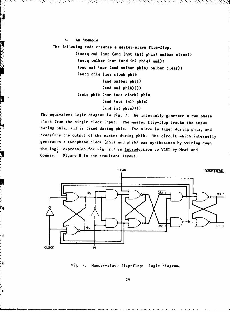
The following code creates a master-slave flip-flop.
((setq oul (nor (and (not inl) phim) oulbar clear))
(setq omlbar (nor (and inl phia) oml))
(out oal (nor (and omlbar phib) ostbar clear))
(setq phia (nor clock phib
(and omlbar phib)
(and oml phib))))
(setq phib (nor (not clock) phis
(and (not inl) phia)
(and inl phia))))The equivalent logic diagram is Fig. 7. We internally generate a two-phase
clock from the single clock input. The master flip-flop tracks the inputduring phia, And is fixed during phib. The slave is fixed during phia, and
transfers the output of the master during phib. The circuit which internallygenerates a two-phase clock (phia and phib) was synthesized by writing down
the logic expression for Fig. 7.7 in Introduction to VLSI by Head an~i
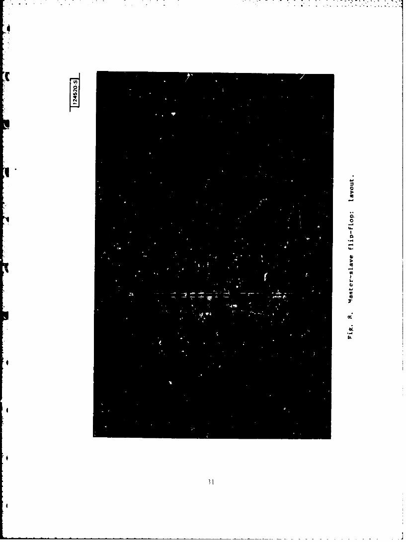
Conway.3 F'igure 8 is the resultant layout.
CLEAR ' 1 N N--
L4
CLOCK IN
Fig. 7. Master-slave flip-flop: logic diagram.
29
'4.
0
4.~
6)
-4
iI
.1.1
S. . . .. . . .. . . . . . . .

7. Summary
LBS is an intermediate-level design specification well matched to MDSIS
..C capabilities. A design specification in LBS average& about 2 gates per
line of code. There is, therefore, no substantial design effort penalty in
using LBS rather than other intermediate-level specification approaches. The
LBS specification can be compiled and recompiled in any technology for which
an LBS synthesizer has been implemented.Ii. The LBS C)MDS synthesizer was designed and implemented in approximately"four man-months. A CMDS design rules change was incorporated in about I man-
week. We estimate that a change to another well-understood technology would
take a&proximately 2 man-months. It is unlikely that the designs could have
been laid out by hand in the time provided, msch less retargeted for the new
rules. The retargetability feature of LBS proves advantageous very quickly
given the pievailing rate of IC fabrication improvements.
33

III. RVLSI TECHNOLOGY
A lateral link has been developed for superposition on the MOSIS NMOS
process. This structure has the advantage of comatibility vith a one-level
metal process. A layer of polyimide insulator is placed on top of a metal
gap and volatized with Lhe laser, leaving a conducting carbon deposit.
Combined with existing laser cutting techniques, this will provide the
ability to make and break signal connections on a MOSIS circuit.
Figure 9 is a scanning electron micrograph of a typical link, after the
s.-ser pulse. It consists of two metal lines, each 15 M wide, and a
separation gap of 2.0 Pm. The layered formation is the crater in the
polyimide. It is indicative of the two-dimensional molecular structure.
Figure 10 is an auger analysis of the laser crater on top of the metal.
It show- that the composition of the conducting material is primarily carbon.
In particular, there is virtually no nitrogen left after the laser heating
proc- sa.
about 1600 U.nks made to date, only two exhibited resistances higher
than '"f. Table I shows the results of a subset of this run. Each entry is
the mean resistance and sigma for 41 links of the specified line width and
gap.
A venicle for demonstration of the use of these links in MOSIS circuits
has bee ;ubmitted for fabrication in the August 1982 run. This project is a
completely uncommitted Weinberger-style gate array. This restructurable
array contains 64 columns, each segmentable in four places, providing up to
256 NOR gates. Each of these one-fourth columns is crossed by 8 tracks for
interconnections between gates.
Figure 11 is a color plot of a small section of such an array. It
contains 4 columns and 4 tracks. The real array contains four structures
like the one shown, but with 64 columns and 8 tracks. These structures are
stacked on top of one another, with the column joined by cut points. In
Fig. 11, the pull-ups at the top of each column can be optionally cut off
with the laser. This increases the number of possible connections to a
35

- . ---.-.
0-4
-4
"40
U
U'I
-4
UU
U)
bO'.4
.4
4
36
4
- � � - .- - - . - - -- - -

to 11~
IL act t 0
I-
o 00
p. .1-. u
u U
N w -
C4 0
(3I/Na U~
K 37
- - -- - - - - - - - -

TABLE I
MEAN RESISTANCES OF POLYIMIDZ LINKS ACROSS VARIOUS STRUCTURES
Gap Width (oan)
1.6 om 2.0 iin 2.4 an 3.0 pa 4.0 at 5.0 omLine Width (ki) (k) (k) (kO) ,k) (kl)
•4 on
Mean 1.04 1.05 1.08Std. deviation 0.108 0.109 0.133
7iimMean 0.854 0.844 0.875Std. deviation 0.106 0.091 0.107
10 umMean 0.634 0.648 n.691 0.735Std. deviation 0.073 0.057 0.071 0.079
15 .W4tan 0.473 0.4!3 0.556 0.645 0.687 0.752Std. deviation 0.257 0.043 0.059 0.058 0.064 0.116
38
F4 J
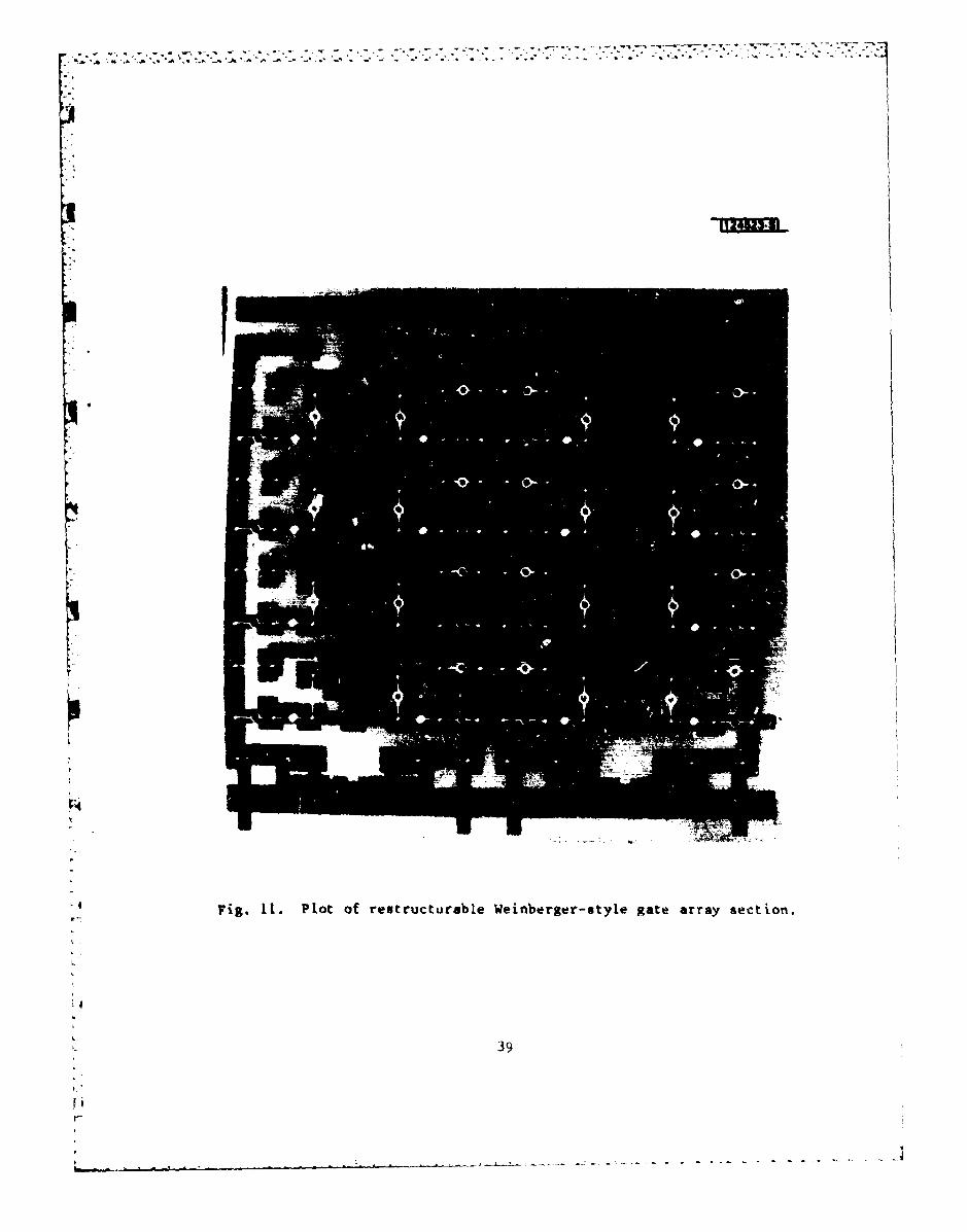
Fig 11-.- Plo of retut l Weinberger-style gate array- section.
I39
0 S
r•
___g I. Po o etucual -JnegrsyeRaearysc~n

• . ., i . . * - .: . o " '/ ; . - - . •. - . .- .. .- - .. -...-.-~- • /- :-. .,--• . .- • . L
neighboring gate (above or below) by sacrificing that gate. At each pull-
down site on the column several laser operations may be performed:
(a) The track crossing that site may be segmented.
(b) The pull-down transistor nay be attached, source to
the column, &ate to the track.
(c) A cross point may be formied between the track and
the column. This is used to tap off the output of
one gate for connection to the input of another.
The first attempt at programing of this array will be to implement a
4-bit aritInetic logic unit slice identical to the classical 74181 TTL part.
The topology of the ALU has been mapped onto the array by hand, but remains
to be switch-level simulated.
41

IV. TESTING
The TOC system is a functional IC tester, consisting of an array of
4-pin slices, together with a small amount of common interface and control
* circuitry. In keeping with the TOC philosophy of dynamic circuit testing,
there is a provision for looping through hold sequences, using one mmory
bank, while the other is being reloaded.
Figure 12 is a block diagram of the TOC system. Each slice consists of
a single custom NMOS circuit (TOC-DUT), and a pair of 4K- by 12-bit static
memories. Rach slice will drive four pins of the device under test (DUT).
The banks are used to hold both the vectors to, and the responses from, the
device under test. One bank is loaded by the host while the other drives the
test sequence.
Test vectors are encoded with three memory bits for each pin (hence the
12 bits for four pins). These three bits form an octal number, or coimmand,
used for indicating what to do with the pin during that state, and logging
* DUT errors.
The other major component of the system is TOC-ADDR. This unit, in
response to a few control inputs supplied by the first slice, will generate
the appropriate addresses for the memory banks.
Testing proceeds as follows:
(a) Characters from the host) containing test vectors in
K octal format, are loaded into the first memory bank
of each slice. The vector list contains a one-time
test, followed by a repeated portion. This second
part can be used to keep dynamic circuits "alive."
(b) The "go" command is issued by the host, and the
first portion of the test is performed, with the
0 results stored in the second memory bank. The host
is informed that either the test was successful, or
that there were errors, and the TOC system starts
looping through the "keep alive" sequence.
43

Ir
q I U)
u z
a -- 4---- c
cQ CC
I~ CI
I LI
K: I_ _ _ _ _ _ _
- 0 [0= p
(nN
44

"(c) During this holding pattern, the host is free to
examine the second memory bank to find out where
errors were, and then load it with the next set of
vectors.
(d) When the "go" command is reissued, the memory banks
switch roles, and the sequence continues with step (b).
This design will apply a test vector every microcycle. Comercially
available memory circuits, suitable for this application, have been selected.
The decision was made to keep the UART for the system off the TOC chip, and
an appropriate part was selected for this function.
One alternative that is being considered is combining the functions of
TOC-DUT and TOC-ADDR into a single chip type. In this implementation, the
TOC chip is really performing two completely different functions. MACPITTS
provides a method for describing these two functions as one design, yet
produces in hardware only the union of the resources used by either, not the
sum. The MACPITTS description of this dual-function TOC chip is under
construction.
45
j

V. APPLICATIONS
A. DIGITAL INTEGRATOR
The digital integrator which is serving as an RVLS1 demonstration
vehicle comprises 236 10-bit counters, an equal number of latches, and input
and output shift registers. It is partitioned into 64 4-counter cells. Two
implementations are in fabrication.
1. Phase 0 Integrator
In the Phase 0 implementation each cell, which is only one 4-bit
counter and associated circuitry, is implemented with a CMDS gate array. A
2-in. wafer contains 49 of these cells with interconnect having a patential
link at every intersection of the horizontal and vertical buses. One of
these wafers was laser linked to build our first wafer-scale device.
Figure 13 is a photograph of this packaged wafer.
Due to the inaccessibility for testing of some of the tracks in the
outside cells, only a 5 x 7 array was usable. The cells were tested on awafer prober and 21 good cells were found. The capacitance of all tracks,both wafer length and cell stubs, was measured; about 3 percent of the tracks
were bad.
A set of programs writ~en to assist in design and fabricution of
another demonstration vehicle, an FFT system, was used for the integrator.
The programs are used to generate descriptions of the logical and physical
devices, analyze test data, and perform assignment and linking. The
algorithms for finding signal paths (linking) are rather simple and oriented
toward the type of nets found in these two systems, i.e., 2-point and bus.
The physical nets can be displayed on a color display and it is possible to
manually intervene in the assignment and linking. This set of programs is
called LSH (Link Shell). "Prom the test results assignment and linking were
performed for a 16-cell system and the results were used by the RWED program
to control the laser restructuring. Laser restructuring proceeded
47

* r c1rr -. -. -. *. N N. ¾ - -% -.- '---w---',. -w j-w-- -. -w
A
NI..a''I
0
0
4J
U
0\JK
a'-- I
I'-I',
49

automatically except for intervention at each cell for testing of the
partially completed wafer and manual realignimnt of the laser table. A
video tape record was made of the entire process. Since testing was
"performed at a low clock rate, only after completion of laser linking was it
discovered that some links had a high impedance which prevented higher speed
operation. Titese links were repaired by a second application of a laser
pul.se.
It appears that the links were made at a laser power level too near the
threshold for linking because of a fear (subsequently determined to be
unfounded) that a higher power might cause dmage to link tabs, and because
the bottom barrier cxide thickness in the link structure was near the
maximum for good linking. On the next wafer more use will be made of the
laser test structures to establish the proper laser power level. Signal
"paths were ýerou~ed around two line-to-substrate shorts which may have been
caused by laser missligmnen•. There were no problems with the cutting of
interconnect metal. During the diagnosti~c and repair process, considerable
use was made of laser probing to help locate high impedance links.
After repairs, one cell could not be cleared bezause of damage incurred
during mechanical probing and one cell does not count, apparently because of
an internal defect. Otherwise, the wafer operates correctly. Wafer testing
was done on the Tektronix 3260 unit which proved quite versatile for
diagnostic evaluation.
From this first experience we are convinced that the interconnect
testing is an important part of the process and the capacitance measurement
appears to be quite an effective way to do the testing. Likewise, testing
during linking is valuable and the importance of doing realistic testing was
demonstrated. Additional Phase G wafers will be processed to completion.
2. Phase 1 Wafer
4
"This wafer will have input and output buffers on the wafer periphery. A
two-level distribution system for the 25-MHz clock will be used and SPICE
simulations show that 25-M4z operations should be achievable with worst-case
.5

. . . ..-.. . . ... " • -? . . '- : _ . . .":•'• •. . ... . .. .. ". -. • '.. . ,. . ., .:- • ....- \ ".
fabrication parameters. Based upon our experience with the Phase 0 wafer,
all tracks are probeable for capacitance measurements. These wafers will be2
packaged in 2.25-in. packages of the type usually used for hybrid circuits.
B. DSP CHIP DESIGNS
1. Systolic Correlators
A systolic correlator for single-bit reference, multi-bit data has been
designed in another group at Lincoln Laboratory. It is cascadable with cell-
to-cell connections in one dimension plus power and clock lines and would
make an interesting RVLSI application for systems which need very long
correlations. With some help from RVLSI personnel, three architecturally
distinct versions of this circuit were designed using in-house CAD tools andfabricated by MOSIS. Some details of these chips are given in Table II.
TABLE II
CUSTOM NMOS SYSTOLIC CORRELATORS
Characteristics Area, Speed, Yield Comments
4 data, I reference bit 2.1 x 4.1 m2
4 samples 5.5 t4Hz Design on CALMA12-bit accumulation 4/5
2 data, I reference bit 3.5 x 3.5 mm
8 samples 4.4 M11z PLA cell5-bit accumulation 2/4
Window correlator 1.2 x 0.8 mm2 Larger andI data, I reference bit I ?41z faster design4 samples 4/4 in fabrication5-bit accumulation
52

S•,.- * .. -.- • - ..• - -;.* ,-.,-------1-.1-... --.--..-. -•,. ...•_ • i- . -.-i ,. •. "'. .: -. -.
2. D)igital AGC Controller
A MACPITTS circuit has been designed to implement the digital control
portion of an automatic gain control (AGC) for the analog-to-digital (A/D)
conversion subsystem of a narrowband speech coder. The input to the circuit
is the digital output of the A/D converter while the circuit's output is adigital value feeding a digitally controlled audio attenuator which
immediately precedes the A/D conventer. Additional inputs to the AGC circuit
include a sample strobe, speech coder frame strobe, and push-to-talk input.
The controller is based on a CCITT standard "fast-attack/slow-decay"
algorithm. The circuit's output or, equivalently, the audio attenuation is
increased when the A/D is observed to be saturating. When the input to the
A/D is at too low a level, the audio attenuation value is decreased.
Constraints are placed on the speed at which the attenuation is decreased in
order to avoid responding to normally occurring gain fluctuations and pauses
in speech. Finally, to maintain the integrity of the speech coders analysis
algorithm, changes in the digital attenuation value occur only at frame
boundaries.2
The circuit's dimensions are 5.4 x 4.5 mm using 4-um rules and
comprisec 2198 transistors. The circuit has passed design rule checking andnode extraction has been completed using the M.I.T. program "node-extract."
Switch-level simulation is in progress using the M.I.T. "nl" program.
C. VECTOR DIGITAL SIGNAL PROCESSOR (VDSP)
1. Introduction
We have been investigating the applicability of a vector-oriented
processor to digital signal processing. If it proves suitable, we will
design it using MACPITTS or LBS in either NMOS or CMOS. The benefit of a
specific application focus is that it provides a slice through all the
problems to be en-ountered in VLSI and RVLSI. Major issues to be addressed
53

include testing and wafer-scale interconnect, plus the development of
additional design tools motivated by actual system requirements.
We are investigating vector processing based on the following chain of
reasoning:
Thesis: The switching speed of MDS devices is such too
slow to build an effective conventional
processor.
Antithesis: NMOS is the easiest technology in which to
design.
Synthesis: We will replace raw speed with parallelism and
hardware control complexity.
Desideratum: Increase in parallelism and hardware
complexity must not be reflected in
programing complexity.
Two methods of achieving the above synthesis that are popular in
microprocessor design Are pipelining and horizontal microcoding. Pipelining
increases throughput, at the expense of control complexity. Unfortunately,
utilizing more than a t. pipelined execution stages in a conventional
instruction architecture causes programming difficulties. Horizontal
microcoding may provide many functional units (adders, mtltipliers, etc.),
allowing the programmer to access and keep all busy in parallel. However,
this method is also known to cause programmer headache. Other methods that
require networks of multiple processors are even more complex to program.
One method that has been used in the high-speed computer world is to combine
pipelining with vectr • ru i . A third method is massively parallel
architectures such as the ILLIAC IV for Single Instruction Multiple Data
(SIMD) programming. Again, this methodology has not matured to the point
that programming a SI14D machine -early as convenient as progranming a
standard machine.
54
2. Vector Processor
The "vector" in vector processor refers to the processor's preferreddeta type, not to the number or topology of processing units. The advantages
of a vector processor are as follows:
(a) Algorithms are often naturally expressed or expressible
mathematically in some vector notation.(b) Vector machines require fewer instruction fetches than
conventional (hereafter referred to as "scalar")
machines.
(c) Vector machines can titilize pipelining without
programmer control complexity. For example, if twovectors are to be muultiplied it is trivially "k•nown" by
the hardware that the result of mut.tiplying the first
two elements is not needed before the next two elements
can be multiplied. This meant that a pipelined
multiplier can be used, with the second pair of
operands being input to the multiplier before the
results from the first pair are available. The vector
machine has increased its multiply throughput to the
limit of the pipelined multiplier, without the
programer being aware of the delay in obtaining the
results.
(d) Due to advantages (b) and (c), the vector processor ian
execute data read/writes nearly every cycle.
3. Program Complexity
We have implied that programming a vector machine is not very much moredifficult than programming a straightforward scalar machine for the same job.
There are very few programmers who would accept that statement without some
55

2o.
support. We have considered the inner loop of three basic digital signal-
processing algorithms: lattice filter cell, second-order section of a
recursive filter bank, and F!r butterfly. These algorithms were coded for
the Lincoln LDSP, a coviventional scaler processor of the single accumulator
type. Because our preliminary vector instruction architecture has a single
accumulator vector, code translation was extremely simple. Almost all LDSP
instructions simply carried over into vector instruction3, removing the
. innermost loop. For example, the lattice filter algorithm is diagramed in
* Fig. 14. The innermost loop in LDSP code is c(ompared to its VDSP equivalent
in Fig. 15. The third instruction in the VDSP code act.ually uses the input
"speechin" value. The corresponding LDSP instruction uses a temporary
variable to accumulate from one loop execution to the next. This means that
a pre-loop setup is necessary to initialize the temporary variable to the"speechin" value (code not shown). Another difference betwen LDSP and VDSP
code is in the behavior of the loop instruction. The VDSP code, of course,
does not have one. However, the LDSP instruction trhat is used has the side
effect of allowing the execution of the next instruction b.fcre it loops
back!
-ThIi2456-NI
S COUTPUT
K.,
T T
Fig. 14. Lattice filter algorithm diagram.
56

- - - . . - . - - -- - - o - - - o . - -, - - - - n , -- t . • ."
LDSP CODE VECTOR PROCESSOR CODE
loop dix BRL T - SRLmulfx KS T - TOKS
add& TRLTMP T 1] -spechinIt& TRLTMP T- + Tmulfx KS T-T*KS
addax BRL T-T+BRLjpzx loopstax BRL+1 T-IT
Fig. 15. Comparison of LDSP and VDSP code for lattice filter.
4. Hardware Architecturee and Chaining
Several hardware architectures for the proposed instruction archi-
tecture are under consideration. These entail trade-offs between memory
cycles dnd control complexity. Fortunately, all will use the same basic
instruction architecture so that programmers will not have to reorient
themselves if the simplest one is built first and higher performance ones
built later. The highest performsnce hardware architecture being considered
uses a technique termed "chrining." Chaining is used by the Cray-I
supercomputer, and its adaptation to our smaller processor may not be
justifiable in terms of the added control overhead.
Chaining involves the dynamic pipelining of two or more instruction
units withini the processing unit. For example, the lattice filter code can
be represented as the data-flow diagram of Fig. 16. If there is a
sufficient supply of multipliers, adders, and other units, internal
interconnect can be dynamically reconfigured to link the output of one unit
5
57

KS SPEECHIN K R
Fig. 16. Lattice filter data-flow diagram.
*to the input of the next without an intermediate write/read vector cycle.
This is advantageous in terms of performance and is concealed from the
programmaer due to the nature of the instruction architecture's single
* accumulator vector.
Even greater performance can be obtained if adiitional adder and
multiplier units are available and the arithmetic expression to be executed
* is longer. On the other hand, the extra units sit idle if the expression is
- shorter. Again, this is all compatible with the same proposed instruction
architecture seen by the programmer.
5. Breakdown of the Instruction Architecture
0 Unfortunately, the full chaining capability cannot be used with the
* instruction architecture. For exaple, consider the second-order section~
* data-flow graph of Fig. 17. The second-order section (and the FFT) have
* data-flow graphs that are much more balanced trees than the lattice filter.
58

I C91 D1 C82 D2 CA2 D2 CA, D,
X X
D1 0 D2
Fig. 17. Second-order section data-flow graph. (Note the balancedtree aspect of the graph compared to the more linear structure cfthe lattice graph.)
The difficulty with the balanced tree is that it cannot be represented as a
chain of single accumulator instructions (without reads and writes to
temporary variables).
In deference to APL, we now refer to the restrictive implications of
the single accumulator architectures as "restricted dyadic." The restrictionV is that only one of the two operands to a dyadic function may be generalexpression, the otl'-: muist be a memory read. When the second-order section
is written for a single accumulator instruction architecture, either vectoror scalar, its performance is considerably degraded. Not only is the full
parallelism no longer utilized, but many additional memory read/write cycles
4 must now be executed.
59

6. Full Dyadic
in view of the advantages of full dyadic (equivalently: full cross-bar
* or full chaining), we have begun to study its hardware and software
implications.
For software, the primary implication is that the LDSP-like single
* accumulator programmers' model must be dropped. The replacement programmers'
* model has not yet been decided on and is the subject of continuing research.
- ~Just as an example of sowe instruction issues, reconsider the data-flow graph
of the second-order section (Fig. 17). Notice that Dl and D2 are both inputs
and outputs. What this means is that Dl and D2 are "master-slav." registers.
The outputs of these registers are fixed wehile the calculations proceed
* through the operations tree. Then the output taps for Dl and D2 are loaded
into the registers and the output tap for 0 is read. The new value for 1 is
* then presented to the operations tree, and the cycle repeats. This sort of
operation in common in digital signal processing (also digital hardware in
general, and in process flow simulations), but such capabilities are seldom
found in programmning languages (among the few languages which do have similar
* ~capabilities are MACPITTS and Dynamo).0
The most straightforward method implementing full chaining in hardware
is to connect a mass of functional units to a large cross-bar switch
(Fig. 17). Examination of the three model algorithms shows that roughly
10 function units and 10 memory ports ccai be kept busy. With 24-bit words
- ~and two input and one output operands per function, the cross-bar size is~
720 x 480. This is too complex, even for wafer-scale integration.
Fortunately, it has been demonstrated theoretically that bit-serial.
arithmetic does not suffer as much degradation as 1/24 compared to the
24-bit, word parallel approach. Due to the wafer-scale approach, the actual
*performance difference should be less, or even reverred. The bit-serial
4 functional units are not as large as the word-parallel so more of the system
* ~can be accoimmodated on a single wafer. This means that inter-unit
communication could be considerably faster than for a printed circuit or
* wire-wrap board level word-parallel design.
60

In order to properly analyze the bit-serial vs word-parallel trade-offs,
we intend to design some function units using our Lincoln Boolean Synthesizer
(Sec. I-C). These designs will then be simulated to estimate their speed
vis-a-vis estimates of word-parallel functional units.
61

REFERENCES
I. Restructurable VLSI Program Semiannual Technical Sumary,Lincoln Laboratory, M.I.T. (31 March 1982), DTIC AD-A120471.
2. A.J. Giovinaizo, "A Mask Design Rule Checking System," Proc.Intl. Conf. on Circuits and Computers (October 1980),pp. 932-936.
3. C.A. Mead and L.A. Conway, Introduction to VLSI Systems(Addison-Wesley, Reading, Massachusetts, 1980).
4. J.M. Siskind, J.R. Southard, and K.W. Crouch, "GeneratingCustom High Performance VLSI Designs from SuccinctAlgorithmic Descriptions," Proc. Conf. on Advanced Researchin VLSI, January 1982.
5. A. Weinberger, "A Large Scale Integration of ADS ComplexLogic: A Layout Method," IEEE JSSC SC-2, 182-190(December 1967).
6. C.E. Leiserson, private communication.
7. JD. Williams, "Sticks - A New Approach to LSI Design,"M.S. Thesis, Department of Electrical Engineering andComputer Sciences, Massachusetts Institute of Technology,June 1977.
8. S.P. Reiss and J.E. Savage, "SLAP - A Silicon LayoutProgram," Brown University Technical Report No. CS-82-17(June 1982).
9. S. Johnson, private communication, July 1982.
10. J.R. Southard, A. Domic, and K.W. Crouch, "LBS - LincolrvBoolean Synthesizer," Technical Report 622, LincolnLaboratory, M.I.T. (1 September 1982), DTIC AD-120999.
FE
62
I .

a UNCLASSIFIED
SECURITY CLASSIFICATION OF THIS PAGE (Vbim Dissii Nossw.
REPORT DOCUMENTATION PAGE ___________________
I. REPORT NUMER j OM ACCEUI 11a I. uECONN CATALOG
4. TITLE (and Subedal) L. "M OF IMPORT A PERSON VEED
Semiannual Technical SummaryRestructurable VLSI Program 1 April - 30 September 1982
s. ý rnouM .wRuinRTm i
7. ALFIOR(s) I. CoanTAC ON SamT EME(s)
Peter E. Blankenship F1962B4IO-C-002
I. PERFORMING ORGANIZATION SAIRE AID ADDRESS It. PROGRAM EILEMENT. PROJECT. TAMLincoln Laboratory, M.I.T. ARPA Order 3797P.O. Bo 7 Program Element No. 61101ELexington. MA 02173-0073 Project No. 2D30
11. CONTROLLING OFFICE OWME A0D ADDRESS 12. IMPORT DATEDefense Advanced Research Projects Agency 30 September 19821400 Wilson Boulevard 13. mumm OF PAGESArlin~gton, VA 22209 70
14. MONITORING AGENCY NAME & ADDRESS (if differeut froms Controfflag Off1ce) is. SECUETY CLASS. (of"th repart)
Electronic Syetems roivision Ucasfe
Hansicom AFB, MIA 01731 16a. DECLASSIFICATION DOWNGRADING SCHEDULE
1S. DISTRIBUTION STATEMENT (of dauis Report)
Approved for public release; distribution unlimited.
17. DISTRIBUTION STATEMENT (a/ the abstract ente~red in Rilcd 201, lfdiffeentn from Report)
18. SUPPLEMENTARY MOTES
None
19. KEY WORDS (Copnsinu do n reverse side if neressmry andi identify by bhod-k number)
VLIcustomnization routingRemtructurable VLSI (RVLSI) hardware description language systolic arrayprogrammable interconnect placement integratordefect avoidance
20. ABSTRACT (Cuntinue, do reiwar " aidf nweesaary and identify by Worek munsiorr)
This report describes work on the Restructurable VLSI Research Program sponsored by) the Informa-tion Proc-essing Techniques Office of the Defense Advanced Research Projects Agency during the semi-
* annual period I April through 30 September 1982.
00 FORM 1473 EDITION OF I1 I'.V 15615 OBSOLETE UNCLASSIFIED1 Jan 73 SECURITY CLASSIFICATION OF THIS PAGE (Whe An, EMi8uAnfgi)