Embed Size (px)
Citation preview
PXI ExpressTM
NI PXIe-1065 User Manual
NI PXIe-1065 User Manual
January 2017371990D-01

Support
Worldwide Technical Support and Product Informationni.com
Worldwide Offices
Visit ni.com/niglobal to access the branch office websites, which provide up-to-date contact information, support phone numbers, email addresses, and current events.
National Instruments Corporate Headquarters
11500 North Mopac Expressway Austin, Texas 78759-3504 USA Tel: 512 683 0100
For further support information, refer to the NI Services appendix. To comment on NI documentation, refer to the NI website at ni.com/info and enter the Info Code feedback.
© 2007–2017 National Instruments. All rights reserved.
Legal Information
Limited WarrantyThis document is provided ‘as is’ and is subject to being changed, without notice, in future editions. For the latest version, refer to ni.com/manuals. NI reviews this document carefully for technical accuracy; however, NI MAKES NO EXPRESS OR IMPLIED WARRANTIES AS TO THE ACCURACY OF THE INFORMATION CONTAINED HEREIN AND SHALL NOT BE LIABLE FOR ANY ERRORS.
NI warrants that its hardware products will be free of defects in materials and workmanship that cause the product to fail to substantially conform to the applicable NI published specifications for one (1) year from the date of invoice.
For a period of ninety (90) days from the date of invoice, NI warrants that (i) its software products will perform substantially in accordance with the applicable documentation provided with the software and (ii) the software media will be free from defects in materials and workmanship.
If NI receives notice of a defect or non-conformance during the applicable warranty period, NI will, in its discretion: (i) repair or replace the affected product, or (ii) refund the fees paid for the affected product. Repaired or replaced Hardware will be warranted for the remainder of the original warranty period or ninety (90) days, whichever is longer. If NI elects to repair or replace the product, NI may use new or refurbished parts or products that are equivalent to new in performance and reliability and are at least functionally equivalent to the original part or product.
You must obtain an RMA number from NI before returning any product to NI. NI reserves the right to charge a fee for examining and testing Hardware not covered by the Limited Warranty.
This Limited Warranty does not apply if the defect of the product resulted from improper or inadequate maintenance, installation, repair, or calibration (performed by a party other than NI); unauthorized modification; improper environment; use of an improper hardware or software key; improper use or operation outside of the specification for the product; improper voltages; accident, abuse, or neglect; or a hazard such as lightning, flood, or other act of nature.
THE REMEDIES SET FORTH ABOVE ARE EXCLUSIVE AND THE CUSTOMER’S SOLE REMEDIES, AND SHALL APPLY EVEN IF SUCH REMEDIES FAIL OF THEIR ESSENTIAL PURPOSE.
EXCEPT AS EXPRESSLY SET FORTH HEREIN, PRODUCTS ARE PROVIDED "AS IS" WITHOUT WARRANTY OF ANY KIND AND NI DISCLAIMS ALL WARRANTIES, EXPRESSED OR IMPLIED, WITH RESPECT TO THE PRODUCTS, INCLUDING ANY IMPLIED WARRANTIES OF MERCHANTABILITY, FITNESS FOR A PARTICULAR PURPOSE, TITLE OR NON-INFRINGEMENT, AND ANY WARRANTIES THAT MAY ARISE FROM USAGE OF TRADE OR COURSE OF DEALING. NI DOES NOT WARRANT, GUARANTEE, OR MAKE ANY REPRESENTATIONS REGARDING THE USE OF OR THE RESULTS OF THE USE OF THE PRODUCTS IN TERMS OF CORRECTNESS, ACCURACY, RELIABILITY, OR OTHERWISE. NI DOES NOT WARRANT THAT THE OPERATION OF THE PRODUCTS WILL BE UNINTERRUPTED OR ERROR FREE.
In the event that you and NI have a separate signed written agreement with warranty terms covering the products, then the warranty terms in the separate agreement shall control.
CopyrightUnder the copyright laws, this publication may not be reproduced or transmitted in any form, electronic or mechanical, including photocopying, recording, storing in an information retrieval system, or translating, in whole or in part, without the prior written consent of National Instruments Corporation.
National Instruments respects the intellectual property of others, and we ask our users to do the same. NI software is protected by copyright and other intellectual property laws. Where NI software may be used to reproduce software or other materials belonging to others, you may use NI software only to reproduce materials that you may reproduce in accordance with the terms of any applicable license or other legal restriction.
End-User License Agreements and Third-Party Legal NoticesYou can find end-user license agreements (EULAs) and third-party legal notices in the following locations:
• Notices are located in the <National Instruments>\_Legal Information and <National Instruments> directories.
• EULAs are located in the <National Instruments>\Shared\MDF\Legal\license directory.
• Review <National Instruments>\_Legal Information.txt for information on including legal information in installers built with NI products.
U.S. Government Restricted RightsIf you are an agency, department, or other entity of the United States Government (“Government”), the use, duplication, reproduction, release, modification, disclosure or transfer of the technical data included in this manual is governed by the Restricted Rights provisions under Federal Acquisition Regulation 52.227-14 for civilian agencies and Defense Federal Acquisition Regulation Supplement Section 252.227-7014 and 252.227-7015 for military agencies.
TrademarksRefer to the NI Trademarks and Logo Guidelines at ni.com/trademarks for more information on NI trademarks.
ARM, Keil, and µVision are trademarks or registered of ARM Ltd or its subsidiaries.
LEGO, the LEGO logo, WEDO, and MINDSTORMS are trademarks of the LEGO Group.
TETRIX by Pitsco is a trademark of Pitsco, Inc.
FIELDBUS FOUNDATION™ and FOUNDATION™ are trademarks of the Fieldbus Foundation.
EtherCAT® is a registered trademark of and licensed by Beckhoff Automation GmbH.
CANopen® is a registered Community Trademark of CAN in Automation e.V.
DeviceNet™ and EtherNet/IP™ are trademarks of ODVA.
Go!, SensorDAQ, and Vernier are registered trademarks of Vernier Software & Technology. Vernier Software & Technology and vernier.com are trademarks or trade dress.
Xilinx is the registered trademark of Xilinx, Inc.
Taptite and Trilobular are registered trademarks of Research Engineering & Manufacturing Inc.
FireWire® is the registered trademark of Apple Inc.
Linux® is the registered trademark of Linus Torvalds in the U.S. and other countries.
Handle Graphics®, MATLAB®, Simulink®, Stateflow®, and xPC TargetBox® are registered trademarks, and Simulink Coder™, TargetBox™, and Target Language Compiler™ are trademarks of The MathWorks, Inc.
Tektronix®, Tek, and Tektronix, Enabling Technology are registered trademarks of Tektronix, Inc.
The Bluetooth® word mark is a registered trademark owned by the Bluetooth SIG, Inc.
The ExpressCard™ word mark and logos are owned by PCMCIA and any use of such marks by National Instruments is under license.
The mark LabWindows is used under a license from Microsoft Corporation. Windows is a registered trademark of Microsoft Corporation in the United States and other countries.
Other product and company names mentioned herein are trademarks or trade names of their respective companies.
Members of the National Instruments Alliance Partner Program are business entities independent from NI and have no agency, partnership, or joint-venture relationship with NI.
PatentsFor patents covering NI products/technology, refer to the appropriate location: Help»Patents in your software, the patents.txt file on your media, or the National Instruments Patent Notice at ni.com/patents.
Export Compliance InformationRefer to the Export Compliance Information at ni.com/legal/export-compliance for the NI global trade compliance policy and how to obtain relevant HTS codes, ECCNs, and other import/export data.
WARNING REGARDING USE OF NATIONAL INSTRUMENTS PRODUCTSYOU ARE ULTIMATELY RESPONSIBLE FOR VERIFYING AND VALIDATING THE SUITABILITY AND RELIABILITY OF THE PRODUCTS WHENEVER THE PRODUCTS ARE INCORPORATED IN YOUR SYSTEM OR APPLICATION, INCLUDING THE APPROPRIATE DESIGN, PROCESS, AND SAFETY LEVEL OF SUCH SYSTEM OR APPLICATION.
PRODUCTS ARE NOT DESIGNED, MANUFACTURED, OR TESTED FOR USE IN LIFE OR SAFETY CRITICAL SYSTEMS, HAZARDOUS ENVIRONMENTS OR ANY OTHER ENVIRONMENTS REQUIRING FAIL-SAFE PERFORMANCE, INCLUDING IN THE OPERATION OF NUCLEAR FACILITIES; AIRCRAFT NAVIGATION; AIR TRAFFIC CONTROL SYSTEMS; LIFE SAVING OR LIFE SUSTAINING SYSTEMS OR SUCH OTHER MEDICAL DEVICES; OR ANY OTHER APPLICATION IN WHICH THE FAILURE OF THE PRODUCT OR SERVICE COULD LEAD TO DEATH, PERSONAL INJURY, SEVERE PROPERTY DAMAGE OR ENVIRONMENTAL HARM (COLLECTIVELY, “HIGH-RISK USES”). FURTHER, PRUDENT STEPS MUST BE TAKEN TO PROTECT AGAINST FAILURES, INCLUDING PROVIDING BACK-UP AND SHUT-DOWN MECHANISMS. NI EXPRESSLY DISCLAIMS ANY EXPRESS OR IMPLIED WARRANTY OF FITNESS OF THE PRODUCTS OR SERVICES FOR HIGH-RISK USES.
© National Instruments | v
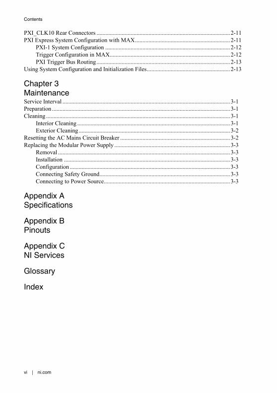
Contents
About This ManualRelated Documentation .................................................................................................... vii
Chapter 1Getting StartedUnpacking......................................................................................................................... 1-1What You Need to Get Started ......................................................................................... 1-1Key Features ..................................................................................................................... 1-2Chassis Description .......................................................................................................... 1-4Optional Equipment.......................................................................................................... 1-5
EMC Filler Panels .................................................................................................... 1-5Rack Mount Kit ........................................................................................................ 1-5Slot Blockers............................................................................................................. 1-5
NI PXIe-1065 Chassis Backplane Overview.................................................................... 1-6Interoperability with CompactPCI............................................................................ 1-6System Controller Slot.............................................................................................. 1-6Hybrid Peripheral Slots ............................................................................................ 1-7PXI Peripheral Slots ................................................................................................. 1-7PXI Express Peripheral Slots.................................................................................... 1-7System Timing Slot .................................................................................................. 1-7PXI Local Bus .......................................................................................................... 1-9PXI Trigger Bus........................................................................................................ 1-10System Reference Clock........................................................................................... 1-10PXIe_SYNC_CTRL ................................................................................................. 1-13
Chapter 2Installation and ConfigurationSafety Information............................................................................................................ 2-1Chassis Cooling Considerations ....................................................................................... 2-2
Providing Adequate Clearance ................................................................................. 2-2Chassis Ambient Temperature Definition ................................................................ 2-3Setting Fan Speed ..................................................................................................... 2-4Installing Filler Panels .............................................................................................. 2-4Installing Slot Blockers ............................................................................................ 2-4
Rack Mounting ................................................................................................................. 2-4Connecting Safety Ground ............................................................................................... 2-4Connecting to Power Source ............................................................................................ 2-5Installing a PXI Express System Controller ..................................................................... 2-5Installing Peripheral Modules........................................................................................... 2-7Power Inhibit Switch LED Indicator ................................................................................ 2-8Remote Voltage Monitoring and Control ......................................................................... 2-9Inhibit Mode Switch ......................................................................................................... 2-10
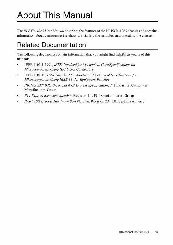
Contents
vi | ni.com
PXI_CLK10 Rear Connectors ..........................................................................................2-11PXI Express System Configuration with MAX................................................................2-11
PXI-1 System Configuration ....................................................................................2-12Trigger Configuration in MAX.................................................................................2-12PXI Trigger Bus Routing..........................................................................................2-13
Using System Configuration and Initialization Files........................................................2-13
Chapter 3MaintenanceService Interval .................................................................................................................3-1Preparation ........................................................................................................................3-1Cleaning ............................................................................................................................3-1
Interior Cleaning .......................................................................................................3-1Exterior Cleaning......................................................................................................3-2
Resetting the AC Mains Circuit Breaker ..........................................................................3-2Replacing the Modular Power Supply ..............................................................................3-3
Removal ....................................................................................................................3-3Installation ................................................................................................................3-3Configuration ............................................................................................................3-3Connecting Safety Ground........................................................................................3-3Connecting to Power Source.....................................................................................3-3
Appendix ASpecifications
Appendix BPinouts
Appendix CNI Services
Glossary
Index
© National Instruments | vii
About This Manual
The NI PXIe-1065 User Manual describes the features of the NI PXIe-1065 chassis and contains information about configuring the chassis, installing the modules, and operating the chassis.
Related DocumentationThe following documents contain information that you might find helpful as you read this manual:
• IEEE 1101.1-1991, IEEE Standard for Mechanical Core Specifications for Microcomputers Using IEC 603-2 Connectors
• IEEE 1101.10, IEEE Standard for Additional Mechanical Specifications for Microcomputers Using IEEE 1101.1 Equipment Practice
• PICMG EXP.0 R1.0 CompactPCI Express Specification, PCI Industrial Computers Manufacturers Group
• PCI Express Base Specification, Revision 1.1, PCI Special Interest Group
• PXI-5 PXI Express Hardware Specification, Revision 2.0, PXI Systems Alliance
© National Instruments | 1-1
1Getting Started
This chapter describes the key features of the NI PXIe-1065 chassis and lists the kit contents and optional equipment you can order from National Instruments.
UnpackingCarefully inspect the shipping container and the chassis for damage. Check for visible damage to the metal work. Check to make sure all handles, hardware, and switches are undamaged. Inspect the inner chassis for any possible damage, debris, or detached components. If damage appears to have been caused during shipment, file a claim with the carrier. Retain the packing material for possible inspection and/or reshipment.
What You Need to Get StartedThe NI PXIe-1065 chassis kit contains the following items:
NI PXIe-1065 chassis
Filler panels
AC power cable—refer to Table 1-1 for AC power cables
NI PXIe-1065 User Manual
Software media with PXI Platform Services 2.0 or higher
Read Me First: Safety and Electromagnetic Compatibility
Chassis number labels
1-2 | ni.com
Chapter 1 Getting Started
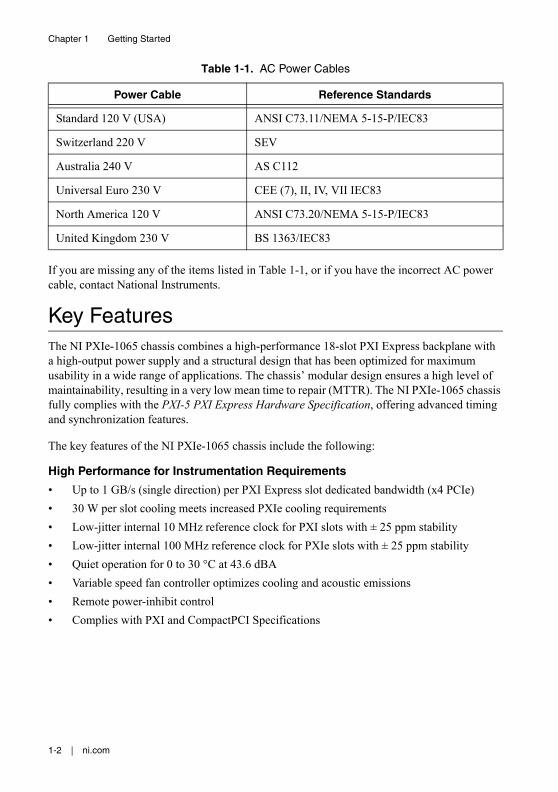
If you are missing any of the items listed in Table 1-1, or if you have the incorrect AC power cable, contact National Instruments.
Key FeaturesThe NI PXIe-1065 chassis combines a high-performance 18-slot PXI Express backplane with a high-output power supply and a structural design that has been optimized for maximum usability in a wide range of applications. The chassis’ modular design ensures a high level of maintainability, resulting in a very low mean time to repair (MTTR). The NI PXIe-1065 chassis fully complies with the PXI-5 PXI Express Hardware Specification, offering advanced timing and synchronization features.
The key features of the NI PXIe-1065 chassis include the following:
High Performance for Instrumentation Requirements
• Up to 1 GB/s (single direction) per PXI Express slot dedicated bandwidth (x4 PCIe)
• 30 W per slot cooling meets increased PXIe cooling requirements
• Low-jitter internal 10 MHz reference clock for PXI slots with ± 25 ppm stability
• Low-jitter internal 100 MHz reference clock for PXIe slots with ± 25 ppm stability
• Quiet operation for 0 to 30 °C at 43.6 dBA
• Variable speed fan controller optimizes cooling and acoustic emissions
• Remote power-inhibit control
• Complies with PXI and CompactPCI Specifications
Table 1-1. AC Power Cables
Power Cable Reference Standards
Standard 120 V (USA) ANSI C73.11/NEMA 5-15-P/IEC83
Switzerland 220 V SEV
Australia 240 V AS C112
Universal Euro 230 V CEE (7), II, IV, VII IEC83
North America 120 V ANSI C73.20/NEMA 5-15-P/IEC83
United Kingdom 230 V BS 1363/IEC83
© National Instruments | 1-3
NI PXIe-1065 User Manual
High Reliability
• 0 to 55 °C extended temperature range
• Power supply, temperature, and fan monitoring
• HALT tested for increased reliability
• Field replaceable power supply shuttle
Multi-Chassis Support
• PXIe System Timing Slot for tight synchronization across chassis
• Rear CLK10 I/O connectors
• Switchless CLK10 routing
Optional Features
• Front and rear rack-mount kits
• Replacement power supply shuttle
• EMC filler panels
• Slot blockers for improved cooling performance
• Factory installation services
1-4 | ni.com
Chapter 1 Getting Started
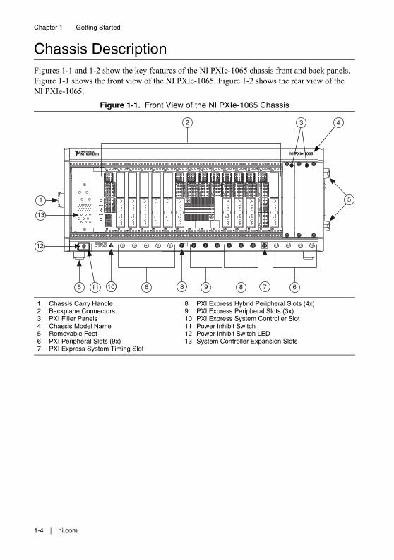
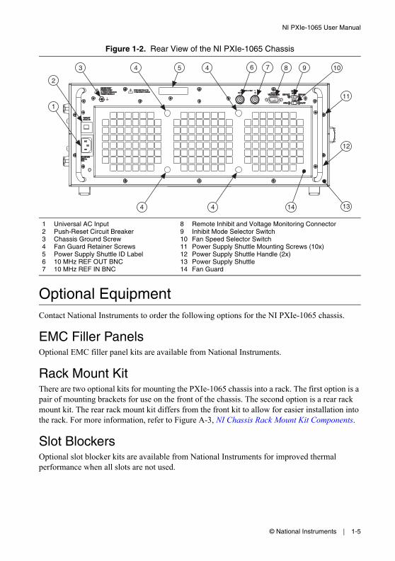
Chassis DescriptionFigures 1-1 and 1-2 show the key features of the NI PXIe-1065 chassis front and back panels. Figure 1-1 shows the front view of the NI PXIe-1065. Figure 1-2 shows the rear view of the NI PXIe-1065.
Figure 1-1. Front View of the NI PXIe-1065 Chassis
1 Chassis Carry Handle2 Backplane Connectors3 PXI Filler Panels4 Chassis Model Name5 Removable Feet6 PXI Peripheral Slots (9x)7 PXI Express System Timing Slot
8 PXI Express Hybrid Peripheral Slots (4x)9 PXI Express Peripheral Slots (3x)10 PXI Express System Controller Slot11 Power Inhibit Switch12 Power Inhibit Switch LED13 System Controller Expansion Slots
181716151312111098765432
NI PXIe-1065
4
8
3
11
1H
14H H H
65 689 7810
2
1
13
5
12
© National Instruments | 1-5
NI PXIe-1065 User Manual
Figure 1-2. Rear View of the NI PXIe-1065 Chassis
Optional EquipmentContact National Instruments to order the following options for the NI PXIe-1065 chassis.
EMC Filler PanelsOptional EMC filler panel kits are available from National Instruments.
Rack Mount KitThere are two optional kits for mounting the PXIe-1065 chassis into a rack. The first option is a pair of mounting brackets for use on the front of the chassis. The second option is a rear rack mount kit. The rear rack mount kit differs from the front kit to allow for easier installation into the rack. For more information, refer to Figure A-3, NI Chassis Rack Mount Kit Components.
Slot BlockersOptional slot blocker kits are available from National Instruments for improved thermal performance when all slots are not used.
1 Universal AC Input2 Push-Reset Circuit Breaker3 Chassis Ground Screw4 Fan Guard Retainer Screws5 Power Supply Shuttle ID Label6 10 MHz REF OUT BNC7 10 MHz REF IN BNC
8 Remote Inhibit and Voltage Monitoring Connector9 Inhibit Mode Selector Switch10 Fan Speed Selector Switch11 Power Supply Shuttle Mounting Screws (10x)12 Power Supply Shuttle Handle (2x)13 Power Supply Shuttle14 Fan Guard
3 4 8
12
1
2
4
5 9
1314
6 7 10
11
4
4
1-6 | ni.com
Chapter 1 Getting Started
NI PXIe-1065 Chassis Backplane OverviewThis section provides an overview of the backplane features for the NI PXIe-1065 chassis.
Interoperability with CompactPCIThe design of the NI PXIe-1065 provides you the flexibility to use the following devices in a single PXI Express chassis:
• PXI Express compatible products
• CompactPCI Express compatible 4-Link system controller products
• CompactPCI Express compatible Type-2 peripheral products
• PXI peripheral products
• Standard CompactPCI peripheral products
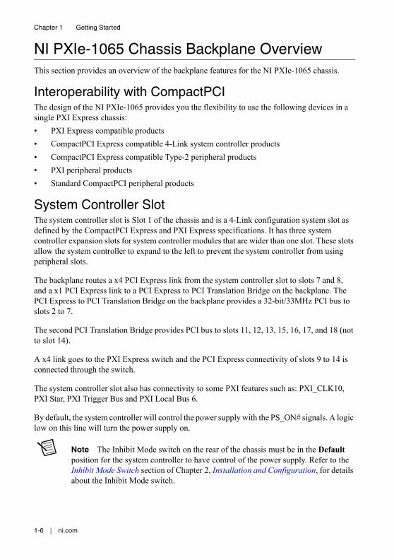
System Controller SlotThe system controller slot is Slot 1 of the chassis and is a 4-Link configuration system slot as defined by the CompactPCI Express and PXI Express specifications. It has three system controller expansion slots for system controller modules that are wider than one slot. These slots allow the system controller to expand to the left to prevent the system controller from using peripheral slots.
The backplane routes a x4 PCI Express link from the system controller slot to slots 7 and 8, and a x1 PCI Express link to a PCI Express to PCI Translation Bridge on the backplane. The PCI Express to PCI Translation Bridge on the backplane provides a 32-bit/33MHz PCI bus to slots 2 to 7.
The second PCI Translation Bridge provides PCI bus to slots 11, 12, 13, 15, 16, 17, and 18 (not to slot 14).
A x4 link goes to the PXI Express switch and the PCI Express connectivity of slots 9 to 14 is connected through the switch.
The system controller slot also has connectivity to some PXI features such as: PXI_CLK10, PXI Star, PXI Trigger Bus and PXI Local Bus 6.
By default, the system controller will control the power supply with the PS_ON# signals. A logic low on this line will turn the power supply on.
Note The Inhibit Mode switch on the rear of the chassis must be in the Default position for the system controller to have control of the power supply. Refer to the Inhibit Mode Switch section of Chapter 2, Installation and Configuration, for details about the Inhibit Mode switch.
© National Instruments | 1-7
NI PXIe-1065 User Manual
Hybrid Peripheral SlotsThe chassis provides four hybrid peripheral slots as defined by the PXI-5 PXI Express Hardware Specification: slot 7 and slots 11 to 13. A hybrid peripheral slot can accept the following peripheral modules:
• A PXI Express Peripheral with x4 or x1 PCI Express link to the system slot or through a switch to the system slot.
• A CompactPCI Express Type-2 Peripheral with x4 or x1 PCI Express link to the system slot or through a switch to the system slot.
• A hybrid-compatible PXI Peripheral module that has been modified by replacing the J2 connector with an XJ4 connector installed in the upper eight rows of J2. Refer to the PXI Express Specification for details. The PXI Peripheral communicates through the backplane’s 32-bit PCI bus.
• A CompactPCI 32-bit peripheral on the backplane’s 32-bit PCI bus.
The hybrid peripheral slots provide full PXI Express functionality and 32-bit PXI functionality except for PXI Local Bus. The hybrid peripheral slot only connects to PXI Local Bus 6 left and right.
PXI Peripheral SlotsThere are nine PXI peripheral slots which will accept PXI or CompactPCI peripherals: slots 2 to 6 and slots 15 to 18. These slots are on the backplane’s 32-bit PCI busses. These slots offer full PXI functionality, but have no PXI Express features. The 64-bit PCI signals on the P2 connectors are not connected.
PXI Express Peripheral SlotsThere are three PXI Express peripheral slots: slots 8 to 10. Slot 8 is directly connected to the system slot with a x4 PCI Express link. Slots 9 and 10 are connected to the system slot through a PCI Express switch. PXI Express peripheral slots can accept the following modules:
• A PXI Express Peripheral with x4 or x1 PCI Express link to the system slot or through a switch to the system slot.
• A CompactPCI Express Type-2 Peripheral with x4 or x1 PCI Express link to the system slot or through a switch to the system slot.
System Timing SlotThe System Timing Slot is slot 14. The system timing slot will accept the following peripheral modules:
• A PXI Express System Timing Module with x4 or x1 PCI Express link to the system slot through a PCIe switch.
• A PXI Express Peripheral with x4 or x1 PCI Express link to the system slot through a PCIe switch.
• A CompactPCI Express Type-2 Peripheral with x4 or x1 PCI Express link to the system slot through a PCIe switch.
1-8 | ni.com
Chapter 1 Getting Started
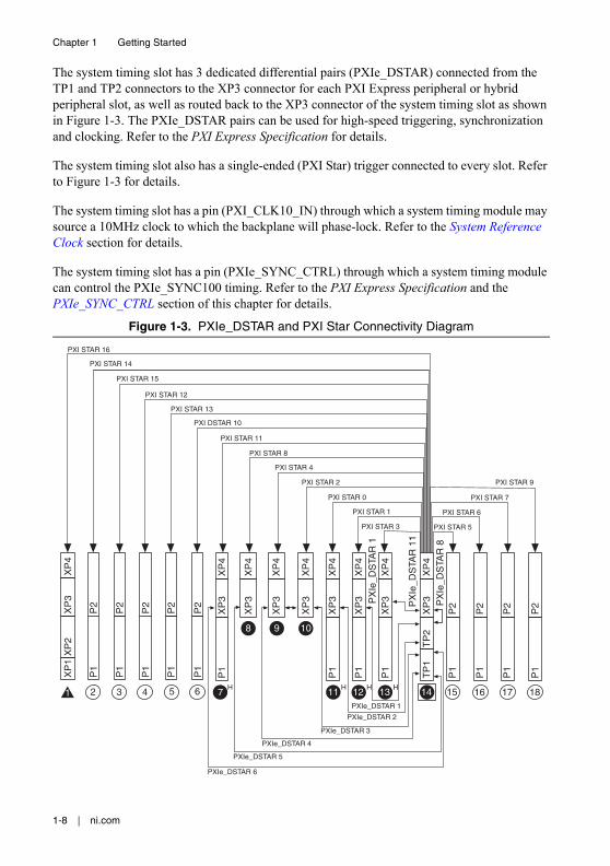
The system timing slot has 3 dedicated differential pairs (PXIe_DSTAR) connected from the TP1 and TP2 connectors to the XP3 connector for each PXI Express peripheral or hybrid peripheral slot, as well as routed back to the XP3 connector of the system timing slot as shown in Figure 1-3. The PXIe_DSTAR pairs can be used for high-speed triggering, synchronization and clocking. Refer to the PXI Express Specification for details.
The system timing slot also has a single-ended (PXI Star) trigger connected to every slot. Refer to Figure 1-3 for details.
The system timing slot has a pin (PXI_CLK10_IN) through which a system timing module may source a 10MHz clock to which the backplane will phase-lock. Refer to the System Reference Clock section for details.
The system timing slot has a pin (PXIe_SYNC_CTRL) through which a system timing module can control the PXIe_SYNC100 timing. Refer to the PXI Express Specification and the PXIe_SYNC_CTRL section of this chapter for details.
Figure 1-3. PXIe_DSTAR and PXI Star Connectivity Diagram
P2
P1
XP
4X
P3
TP
2T
P1
P2
P1
P2
P1
P2
P1
P1
P1
P1
XP
4X
P3
XP
4X
P3
XP
4X
P3
XP
4X
P3
XP
4X
P3
XP
4X
P3
XP
4X
P3
P2
P1
P2
P1
P2
P1
P2
P1
P2
P1
P1
XP
4X
P3
XP
2X
P1
PX
Ie_D
STA
R 1
1
PX
Ie_D
STA
R 8
PXIe_DSTAR 6
PXIe_DSTAR 5
PXIe_DSTAR 3
PXIe_DSTAR 2
PXIe_DSTAR 1
PX
Ie_D
STA
R 1
PXIe_DSTAR 4
PXI STAR 3
PXI STAR 1
PXI STAR 2 PXI STAR 9
PXI STAR 7
PXI STAR 6
PXI STAR 5
PXI STAR 4
PXI STAR 8
PXI STAR 11
PXI DSTAR 10
PXI STAR 13
PXI STAR 12
PXI STAR 15
PXI STAR 14
PXI STAR 16
PXI STAR 0
1
8 9 10
7H 11 H H12 H13 14 1565432 16 17 18
© National Instruments | 1-9
NI PXIe-1065 User Manual
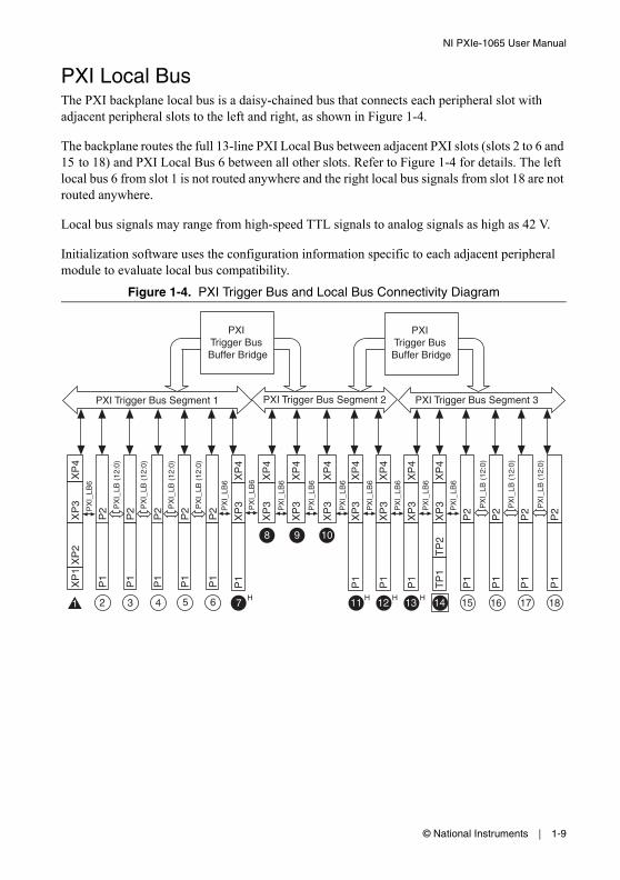
PXI Local BusThe PXI backplane local bus is a daisy-chained bus that connects each peripheral slot with adjacent peripheral slots to the left and right, as shown in Figure 1-4.
The backplane routes the full 13-line PXI Local Bus between adjacent PXI slots (slots 2 to 6 and 15 to 18) and PXI Local Bus 6 between all other slots. Refer to Figure 1-4 for details. The left local bus 6 from slot 1 is not routed anywhere and the right local bus signals from slot 18 are not routed anywhere.
Local bus signals may range from high-speed TTL signals to analog signals as high as 42 V.
Initialization software uses the configuration information specific to each adjacent peripheral module to evaluate local bus compatibility.
Figure 1-4. PXI Trigger Bus and Local Bus Connectivity Diagram
P2
P1
XP
4X
P3
TP
2T
P1
P2
P1
P2
P1
P2
P1
P1
P1
P1
XP
4X
P3
XP
4X
P3
XP
4X
P3
XP
4X
P3
XP
4X
P3
XP
4X
P3
XP
4X
P3
P2
P1
P2
P1
P2
P1
P2
P1
P2
P1
P1
XP
4X
P3
XP
2X
P1
PX
I_LB
6
PX
I_LB
6
PX
I_LB
6
PX
I_LB
6
PX
I_LB
6
PX
I_LB
6
PX
I_LB
6
PX
I_LB
6
PX
I_LB
6
PX
I_LB
6
PX
I_LB
(12
:0)
PX
I_LB
(12
:0)
PX
I_LB
(12
:0)
PX
I_LB
(12
:0)
PX
I_LB
(12
:0)
PX
I_LB
(12
:0)
PX
I_LB
(12
:0)
PXI Trigger Bus Buffer Bridge
PXI Trigger Bus Buffer Bridge
PXI Trigger Bus Segment 1 PXI Trigger Bus Segment 2 PXI Trigger Bus Segment 3
1
8 9 10
7H 11 H H12 H13 14 1565432 16 17 18
1-10 | ni.com
Chapter 1 Getting Started
PXI Trigger BusAll slots on the same PXI bus segment share eight PXI trigger lines. You can use these trigger lines in a variety of ways. For example, you can use triggers to synchronize the operation of several different PXI peripheral modules. In other applications, one module located in the system timing slot can control carefully timed sequences of operations performed on other modules in the system. Modules can pass triggers to one another, allowing precisely timed responses to asynchronous external events the system is monitoring or controlling.
The PXI trigger lines from adjacent PXI trigger bus segments can be routed in either direction across the PXI trigger bridges through buffers. This allows you to send trigger signals to, and receive trigger signals from, every slot in the chassis. Static trigger routing (user-specified line and directional assignments) can be configured through Measurement & Automation Explorer (MAX). Dynamic routing of triggers (automatic line assignments) is supported through certain National Instruments drivers like NI-DAQmx.
Note Although any trigger line may be routed in either direction, it cannot be routed in more than one direction at a time.
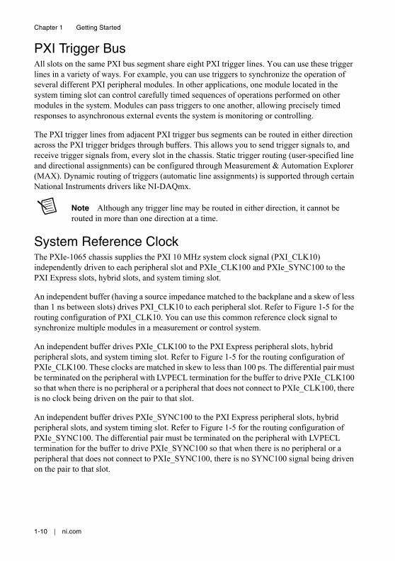
System Reference ClockThe PXIe-1065 chassis supplies the PXI 10 MHz system clock signal (PXI_CLK10) independently driven to each peripheral slot and PXIe_CLK100 and PXIe_SYNC100 to the PXI Express slots, hybrid slots, and system timing slot.
An independent buffer (having a source impedance matched to the backplane and a skew of less than 1 ns between slots) drives PXI_CLK10 to each peripheral slot. Refer to Figure 1-5 for the routing configuration of PXI_CLK10. You can use this common reference clock signal to synchronize multiple modules in a measurement or control system.
An independent buffer drives PXIe_CLK100 to the PXI Express peripheral slots, hybrid peripheral slots, and system timing slot. Refer to Figure 1-5 for the routing configuration of PXIe_CLK100. These clocks are matched in skew to less than 100 ps. The differential pair must be terminated on the peripheral with LVPECL termination for the buffer to drive PXIe_CLK100 so that when there is no peripheral or a peripheral that does not connect to PXIe_CLK100, there is no clock being driven on the pair to that slot.
An independent buffer drives PXIe_SYNC100 to the PXI Express peripheral slots, hybrid peripheral slots, and system timing slot. Refer to Figure 1-5 for the routing configuration of PXIe_SYNC100. The differential pair must be terminated on the peripheral with LVPECL termination for the buffer to drive PXIe_SYNC100 so that when there is no peripheral or a peripheral that does not connect to PXIe_SYNC100, there is no SYNC100 signal being driven on the pair to that slot.
© National Instruments | 1-11
NI PXIe-1065 User Manual
Figure 1-5. Distribution of PXI_CLK10, PXIe_CLK100, and PXIe_SYNC100
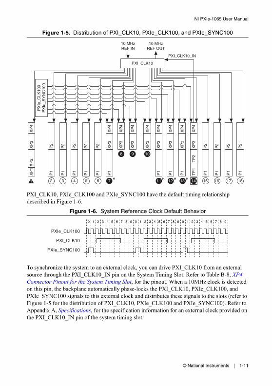
PXI_CLK10, PXIe_CLK100 and PXIe_SYNC100 have the default timing relationship described in Figure 1-6.
Figure 1-6. System Reference Clock Default Behavior
To synchronize the system to an external clock, you can drive PXI_CLK10 from an external source through the PXI_CLK10_IN pin on the System Timing Slot. Refer to Table B-8, XP4 Connector Pinout for the System Timing Slot, for the pinout. When a 10MHz clock is detected on this pin, the backplane automatically phase-locks the PXI_CLK10, PXIe_CLK100, and PXIe_SYNC100 signals to this external clock and distributes these signals to the slots (refer to Figure 1-5 for the distribution of PXI_CLK10, PXIe_CLK100 and PXIe_SYNC100). Refer to Appendix A, Specifications, for the specification information for an external clock provided on the PXI_CLK10_IN pin of the system timing slot.
P2
P1
XP
4X
P3
TP
2T
P1
P2
P1
P2
P1
P2
P1
P1
P1
P1
XP
4X
P3
XP
4X
P3
XP
4X
P3
XP
4X
P3
XP
4X
P3
XP
4X
P3
XP
4X
P3
P2
P1
P2
P1
P2
P1
P2
P1
P2
P1
XP
4X
P3
XP
2X
P1
P1
10 MHzREF IN
10 MHzREF OUT
PXI_CLK10_IN
1
8 9 10
PX
Ie_C
LK10
0P
XIe
_SY
NC
100
PXI_CLK10
7H 11 H H12 H13 14 1565432 16 17 18
PXIe_CLK100
PXI_CLK10
PXIe_SYNC100
0 1 2 3 4 5 6 7 8 9 0 1 2 3 4 5 6 7 8 9 0 1 2 3 4 5 6 7 8 9
1-12 | ni.com
Chapter 1 Getting Started
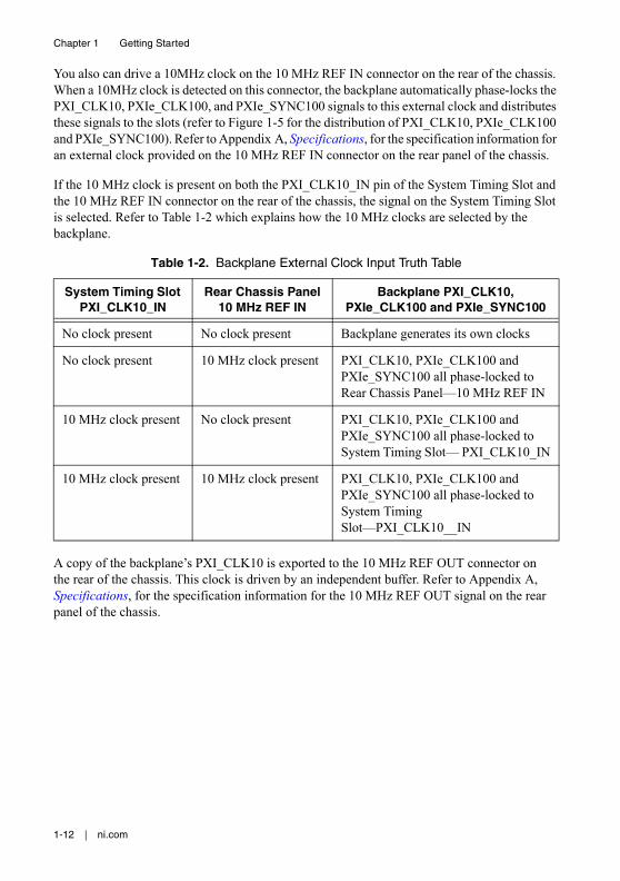
You also can drive a 10MHz clock on the 10 MHz REF IN connector on the rear of the chassis. When a 10MHz clock is detected on this connector, the backplane automatically phase-locks the PXI_CLK10, PXIe_CLK100, and PXIe_SYNC100 signals to this external clock and distributes these signals to the slots (refer to Figure 1-5 for the distribution of PXI_CLK10, PXIe_CLK100 and PXIe_SYNC100). Refer to Appendix A, Specifications, for the specification information for an external clock provided on the 10 MHz REF IN connector on the rear panel of the chassis.
If the 10 MHz clock is present on both the PXI_CLK10_IN pin of the System Timing Slot and the 10 MHz REF IN connector on the rear of the chassis, the signal on the System Timing Slot is selected. Refer to Table 1-2 which explains how the 10 MHz clocks are selected by the backplane.
A copy of the backplane’s PXI_CLK10 is exported to the 10 MHz REF OUT connector on the rear of the chassis. This clock is driven by an independent buffer. Refer to Appendix A, Specifications, for the specification information for the 10 MHz REF OUT signal on the rear panel of the chassis.
Table 1-2. Backplane External Clock Input Truth Table
System Timing Slot PXI_CLK10_IN
Rear Chassis Panel10 MHz REF IN
Backplane PXI_CLK10, PXIe_CLK100 and PXIe_SYNC100
No clock present No clock present Backplane generates its own clocks
No clock present 10 MHz clock present PXI_CLK10, PXIe_CLK100 and PXIe_SYNC100 all phase-locked to Rear Chassis Panel—10 MHz REF IN
10 MHz clock present No clock present PXI_CLK10, PXIe_CLK100 and PXIe_SYNC100 all phase-locked to System Timing Slot— PXI_CLK10_IN
10 MHz clock present 10 MHz clock present PXI_CLK10, PXIe_CLK100 and PXIe_SYNC100 all phase-locked to System Timing Slot—PXI_CLK10__IN
© National Instruments | 1-13
NI PXIe-1065 User Manual
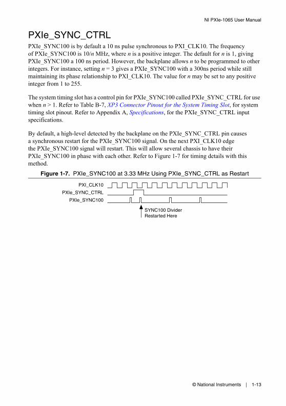
PXIe_SYNC_CTRLPXIe_SYNC100 is by default a 10 ns pulse synchronous to PXI_CLK10. The frequency of PXIe_SYNC100 is 10/n MHz, where n is a positive integer. The default for n is 1, giving PXIe_SYNC100 a 100 ns period. However, the backplane allows n to be programmed to other integers. For instance, setting n = 3 gives a PXIe_SYNC100 with a 300ns period while still maintaining its phase relationship to PXI_CLK10. The value for n may be set to any positive integer from 1 to 255.
The system timing slot has a control pin for PXIe_SYNC100 called PXIe_SYNC_CTRL for use when n > 1. Refer to Table B-7, XP3 Connector Pinout for the System Timing Slot, for system timing slot pinout. Refer to Appendix A, Specifications, for the PXIe_SYNC_CTRL input specifications.
By default, a high-level detected by the backplane on the PXIe_SYNC_CTRL pin causes a synchronous restart for the PXIe_SYNC100 signal. On the next PXI_CLK10 edge the PXIe_SYNC100 signal will restart. This will allow several chassis to have their PXIe_SYNC100 in phase with each other. Refer to Figure 1-7 for timing details with this method.
Figure 1-7. PXIe_SYNC100 at 3.33 MHz Using PXIe_SYNC_CTRL as Restart
PXI_CLK10
PXIe_SYNC_CTRL
PXIe_SYNC100
SYNC100 DividerRestarted Here
© National Instruments | 2-1
2Installation and Configuration
This chapter describes how to prepare and operate the NI PXIe-1065 chassis.
Before connecting the chassis to a power source, read this chapter and the Read Me First: Safety and Electromagnetic Compatibility document included with your kit.
Safety Information
Caution Before undertaking any troubleshooting, maintenance, or exploratory procedure, carefully read the following caution notices.
This equipment contains voltage hazardous to human life and safety, and is capable of inflicting personal injury.
• Chassis Grounding—The chassis requires a connection from the premise wire safety ground to the chassis ground. The earth safety ground must be connected during use of this equipment to minimize shock hazards. Refer to the Connecting Safety Ground section for instructions on connecting safety ground.
• Live Circuits—Operating personnel and service personnel must not remove protective covers when operating or servicing the chassis. Adjustments and service to internal components must be undertaken by qualified service technicians. During service of this product, the mains connector to the premise wiring must be disconnected. Dangerous voltages may be present under certain conditions; use extreme caution.
• Explosive Atmosphere—Do not operate the chassis in conditions where flammable gases are present. Under such conditions, this equipment is unsafe and may ignite the gases or gas fumes.
• Part Replacement—Only service this equipment with parts that are exact replacements, both electrically and mechanically. Contact National Instruments for replacement part information. Installation of parts with those that are not direct replacements may cause harm to personnel operating the chassis. Furthermore, damage or fire may occur if replacement parts are unsuitable.
• Modification—Do not modify any part of the chassis from its original condition. Unsuitable modifications may result in safety hazards.
2-2 | ni.com
Chapter 2 Installation and Configuration
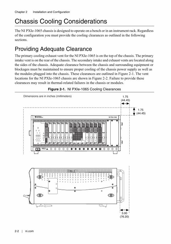
Chassis Cooling ConsiderationsThe NI PXIe-1065 chassis is designed to operate on a bench or in an instrument rack. Regardless of the configuration you must provide the cooling clearances as outlined in the following sections.
Providing Adequate ClearanceThe primary cooling exhaust vent for the NI PXIe-1065 is on the top of the chassis. The primary intake vent is on the rear of the chassis. The secondary intake and exhaust vents are located along the sides of the chassis. Adequate clearance between the chassis and surrounding equipment or blockages must be maintained to ensure proper cooling of the chassis power supply as well as the modules plugged into the chassis. These clearances are outlined in Figure 2-1. The vent locations for the NI PXIe-1065 chassis are shown in Figure 2-2. Failure to provide these clearances may result in thermal-related failures in the chassis or modules.
Figure 2-1. NI PXIe-1065 Cooling Clearances
181716151312111098765432
NI PXIe-1065
1H
14H H H
1.75(44.45)
1.75 (44.45)
3.00(76.20)
Dimensions are in inches (millimeters)
© National Instruments | 2-3
NI PXIe-1065 User Manual
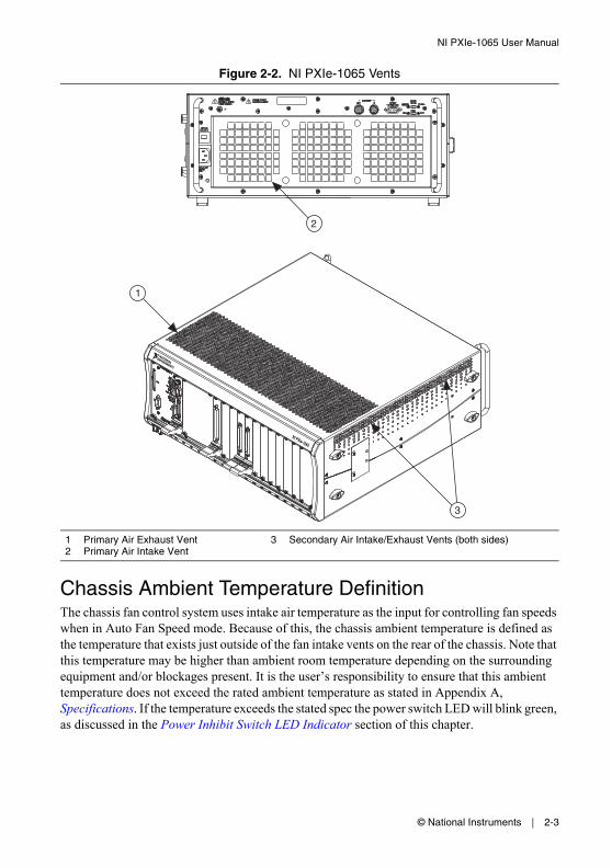
Figure 2-2. NI PXIe-1065 Vents
Chassis Ambient Temperature DefinitionThe chassis fan control system uses intake air temperature as the input for controlling fan speeds when in Auto Fan Speed mode. Because of this, the chassis ambient temperature is defined as the temperature that exists just outside of the fan intake vents on the rear of the chassis. Note that this temperature may be higher than ambient room temperature depending on the surrounding equipment and/or blockages present. It is the user’s responsibility to ensure that this ambient temperature does not exceed the rated ambient temperature as stated in Appendix A, Specifications. If the temperature exceeds the stated spec the power switch LED will blink green, as discussed in the Power Inhibit Switch LED Indicator section of this chapter.
1 Primary Air Exhaust Vent2 Primary Air Intake Vent
3 Secondary Air Intake/Exhaust Vents (both sides)
2
3
1
NI PXIe-1065
2-4 | ni.com
Chapter 2 Installation and Configuration
Setting Fan SpeedThe fan-speed selector switch is on the rear panel of the NI PXIe-1065 chassis. Refer to Figure 1-2, Rear View of the NI PXIe-1065 Chassis, to locate the fan-speed selector switch. Select High for maximum cooling performance or Auto for improved acoustic performance. When set to Auto, the fan speed is determined by chassis intake air temperature.
Installing Filler PanelsTo maintain proper module cooling performance, install filler panels (provided with the chassis) in unused or empty slots. Secure with the captive mounting screws provided.
Installing Slot BlockersThe cooling performance of the chassis can be improved by installing optional slot blockers. Refer to ni.com for more details.
Rack MountingRack mount applications require the optional rack mount kits available from National Instruments. Refer to the instructions supplied with the rack mount kits to install your NI PXIe-1065 chassis in an instrument rack. Refer to Figure A-3, NI Chassis Rack Mount Kit Components.
Note You may want to remove the feet from the NI PXIe-1065 chassis when rack mounting. To do so, remove the screws holding the feet in place.
Connecting Safety Ground
Caution The NI PXIe-1065 chassis are designed with a three-position NEMA 5-15 style plug for the U.S. that connects the ground line to the chassis ground. To minimize shock hazard, make sure the electrical power outlet you use to power the chassis has an appropriate earth safety ground.
If your power outlet does not have an appropriate ground connection, you must connect the premise safety ground to the chassis grounding screw located on the rear panel. Refer to Figure 1-2, Rear View of the NI PXIe-1065 Chassis, to locate the chassis grounding screw. To connect the safety ground, complete the following steps:
1. Connect a 16 AWG (1.3 mm) wire to the chassis grounding screw using a grounding lug. The wire must have green insulation with a yellow stripe or must be noninsulated (bare).
2. Attach the opposite end of the wire to permanent earth ground using toothed washers or a toothed lug.
© National Instruments | 2-5
NI PXIe-1065 User Manual
Connecting to Power Source
Caution Do not install modules prior to performing the following power-on test.
To completely remove power, you must disconnect the AC power cable.
Attach input power through the rear AC inlet using the appropriate AC power cable supplied. Refer to Figure 1-2, Rear View of the NI PXIe-1065 Chassis, to locate the AC inlet.
The Inhibit Mode switch allows you to power on the chassis or place it in standby mode. Set the Inhibit Mode switch on the back of the chassis to the Manual position. Observe that all fans become operational and the power switch LED is a steady green. Switching the Inhibit Mode switch to the Default position allows the system controller to control the power supply.
Installing a PXI Express System ControllerThis section contains general installation instructions for installing a PXI Express system controller in a NI PXIe-1065 chassis. Refer to your PXI Express system controller user manual for specific instructions and warnings. To install a system controller, complete the following steps:
1. Connect the AC power source to the PXI Express chassis before installing the system controller. The AC power cord grounds the chassis and protects it from electrical damage while you install the system controller.
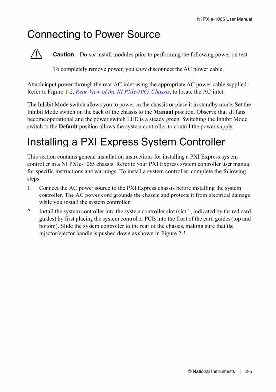
2. Install the system controller into the system controller slot (slot 1, indicated by the red card guides) by first placing the system controller PCB into the front of the card guides (top and bottom). Slide the system controller to the rear of the chassis, making sure that the injector/ejector handle is pushed down as shown in Figure 2-3.
2-6 | ni.com
Chapter 2 Installation and Configuration
Figure 2-3. Installing a PXIe System Controller
3. When you begin to feel resistance, pull up on the injector/ejector handle to seat the system controller fully into the chassis frame. Secure the system controller front panel to the chassis using the system controller front-panel mounting screws.
4. Connect the keyboard, mouse, and monitor to the appropriate connectors. Connect devices to ports as required by your system configuration.
5. Power on the chassis. Verify that the system controller boots. If the system controller does not boot, refer to your system controller user manual.
1 NI PXI Express System Controller2 NI PXIe-1065 Chassis
3 Injector/Ejector Handle4 System Controller Front Panel Mounting Screws (4x)
3
1
4
2
NI PXIe-1065
© National Instruments | 2-7
NI PXIe-1065 User Manual
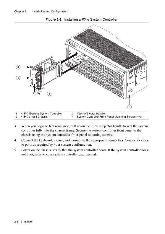
Figure 2-4 shows a PXI Express system controller installed in the system controller slot of a NI PXIe-1065 chassis. You can place CompactPCI, CompactPCI Express, PXI, or PXI Express modules in other slots depending on the slot type.
Figure 2-4. NI PXI Express System Controller Installed in a NI PXIe-1065 Chassis
Installing Peripheral Modules
Caution The NI PXIe-1065 chassis has been designed to accept a variety of peripheral module types in different slots. To prevent damage to the chassis, ensure that the peripheral module is being installed into a slot designed to accept it. Refer to Chapter 1, Getting Started, for a description of the various slot types.
This section contains general installation instructions for installing a peripheral module in a NI PXIe-1065 chassis. Refer to your peripheral module user manual for specific instructions and warnings. To install a module, complete the following steps:
1. Connect the AC power source to the PXI Express chassis before installing the module. The AC power cord grounds the chassis and protects it from electrical damage while you install the module.
2. Ensure that the chassis is powered off.
1 NI PXIe-1065 Chassis 2 NI PXIe System Controller 3 Injector/Ejector Rail
1
2
3
NI PXIe-1065
2-8 | ni.com
Chapter 2 Installation and Configuration
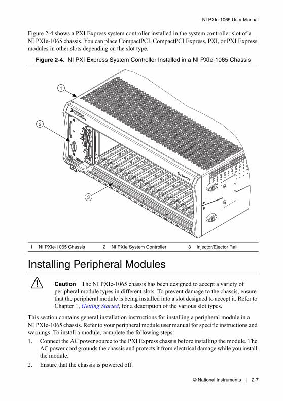
3. Install a module into a chassis slot by first placing the module card PCB into the front of the card guides (top and bottom), as shown in Figure 2-5. Slide the module to the rear of the chassis, making sure that the injector/ejector handle is pushed down as shown in Figure 2-3.
4. When you begin to feel resistance, push up on the injector/ejector handle to fully seat the module into the chassis frame. Secure the module front panel to the chassis using the module front-panel mounting screws.
Figure 2-5. Installing PXI, PXI Express, or CompactPCI Peripheral Modules
Power Inhibit Switch LED IndicatorThe chassis power inhibit switch has an integrated LED. This LED indicates one of four different conditions:
• If the inhibit switch LED is steady green (not flashing), the chassis is powered on and operating normally.
• If the inhibit switch LED is flashing green, the air-intake temperature has exceeded the chassis operating range.
1 Peripheral Module Front Panel Mounting Screws (2x)2 NI PXI Express System Controller3 NI PXIe-1065 Chassis
4 Injector/Ejector Rail5 Injector/Ejector Handle6 PXI Peripheral Module
3
2
4
NI PXIe-1065
1
6
5
© National Instruments | 2-9
NI PXIe-1065 User Manual
• If the inhibit switch LED is flashing red, the power supply outputs are not within voltage regulation requirements.
• If the inhibit switch LED is steady red, the system fans or power supply fan has failed. The remaining fans will automatically be driven high.
Note If two system fans or both of the power supply fans fail the chassis will shut down automatically, preventing the chassis and modules from damage due to overheating.
Remote Voltage Monitoring and ControlThe NI PXIe-1065 chassis supports remote voltage monitoring and inhibiting through a female 9-pin D-SUB (DB-9) connector located on the rear panel. Table 2-1 shows the pinout of the 9-pin D-SUB (DB-9) connector.
Caution When connecting digital voltmeter probes to the rear 9-pin D-SUB (DB-9) connector, be careful not to short the probe leads together. Doing so could damage the power supply.
Table 2-1. Remote Inhibit and Voltage Monitoring Connector Pinout
DB-9 Pin Signal
1 Logic Ground
2 +5 VDC
3 Reserved
4 +3.3 VDC
5 Inhibit (Active Low)
6 +12 VDC
7 Reserved
8 -12 VDC
9 Logic Ground
1 2 3 4 5
6 97 8
2-10 | ni.com
Chapter 2 Installation and Configuration
You can use a digital voltmeter to ensure all voltage levels in the NI PXIe-1065 chassis are within the allowable limits. Referring to Table 2-2, connect one lead of the voltmeter to a supply pin on the remote voltage monitoring connector (9-pin D-SUB) on the rear panel. Refer to Table 2-1 for a pinout diagram of the remote voltage monitoring connector. Connect the reference lead of the voltmeter to one of the ground pins. Compare each voltage reading to the values listed in Table 2-2.
Note Use the rear-panel 9-pin D-SUB connector to check voltages only. Do not use the connector to supply power to external devices.
If the voltages fall within the specified ranges, the chassis complies with the CompactPCI voltage-limit specifications.
Inhibit Mode SwitchOn the rear panel of the chassis there is an Inhibit Mode switch. Refer to Figure 1-2, Rear View of the NI PXIe-1065 Chassis, for the location. The Inhibit Mode switch is recessed to prevent it from accidentally being switched.
The Inhibit Mode switch should be in the Default position when normal power inhibit switch functionality is desired. If the user needs to power on a chassis without a system controller installed the switch should be in the Manual position.
When the Inhibit Mode switch is set to the Manual position, the power supplies are enabled, and you can use the Inhibit signal (active low) on pin 5 of the Remote Inhibit and Voltage Monitoring connector to power off the chassis. To remotely power off the chassis, connect the Inhibit pin (pin 5) to a Logic Ground pin (pin 1 or 9). As long as this connection exists, the chassis will remain off (standby); when you remove this connection, the chassis turns on.
Note For the Remote Inhibit signal to control the On/Off (standby) state of the chassis, the Inhibit Mode switch must be in the Manual position.
Table 2-2. Power Supply Voltages at Voltage Monitoring Connector (DB-9)
Pin Supply Acceptable Voltage Range
2 +5 V 4.75 to 5.25 V
4 +3.3 V 3.135 to 3.465 V
6 +12 V 11.4 to 12.6 V
8 -12 V -12.6 to -11.4 V
1, 9 Logic Ground 0 V
© National Instruments | 2-11
NI PXIe-1065 User Manual
PXI_CLK10 Rear ConnectorsThere are two BNC connectors on the rear of the NI PXIe-1065 chassis for PXI_CLK10. The connectors are labeled IN and OUT. You can use them for supplying the backplane with PXI_CLK10 or routing the backplane’s PXI_CLK10 to another chassis. Refer to the System Reference Clock section of Chapter 1, Getting Started, for details about these signals.
PXI Express System Configuration with MAXThe PXI Platform Services software included with your chassis automatically identifies your PXI Express system components to generate a pxiesys.ini file. You can configure your entire PXI system and identify PXI-1 chassis through Measurement & Automation Explorer (MAX), included with your system controller. MAX creates the pxiesys.ini and pxisys.ini file, which define your PXI system parameters. MAX also provides an interface to route and reserve triggers so dynamic routing, through drivers such as DAQmx, avoids double-driving and potentially damaging trigger lines. For more information about routing and reserving PXI triggers, refer to KnowledgeBase 3TJDOND8 at ni.com/support.
The configuration steps for single or multiple-chassis systems are the same.
Figure 2-6. Multichassis Configuration in MAX
2-12 | ni.com
Chapter 2 Installation and Configuration
PXI-1 System Configuration1. Launch MAX.
2. In the Configuration tree, click the Devices and Interfaces branch to expand it.
3. If the PXI system controller has not yet been configured, it is labeled PXI System (Unidentified). Right-click this entry to display the pop-up menu, then select the appropriate system controller model from the Identify As submenu.
4. Click the PXI system controller. The chassis (or multiple chassis, in a multichassis configuration) is listed below it. Identify each chassis by right-clicking its entry, then selecting the appropriate chassis model through the Identify As submenu. Further expanding the PXI System branch shows all devices in the system that can be recognized by NI-VISA. When your system controller and all your chassis are identified, the required pxisys.ini file is complete.
The PXI specification allows for many combinations of PXI chassis and system modules. To assist system integrators, the manufacturers of PXI chassis and system modules must document the capabilities of their products. PXI Express devices must provide a driver and .ini file for identification. These files are provided as part of the PXI Platform Services software included with your system controller. The minimum documentation requirements for PXI-1 are contained in .ini files, which consist of ASCII text. System integrators, configuration utilities, and device drivers can use these .ini files.
The capability documentation for a PXI-1 chassis is contained in a chassis.ini file provided by the chassis manufacturer. The information in this file is combined with information about the system controller to create a single PXI-1 system initialization file called pxisys.ini (PXI System Initialization). The NI system controller uses MAX to generate the pxisys.ini file from the chassis.ini file.
Device drivers and other utility software read the pxiesys.ini and pxisys.ini file to obtain system information. For detailed information about initialization files, refer to the PXI specification at www.pxisa.org.
Trigger Configuration in MAXEach chassis has one or more trigger buses, each with eight lines numbered 0 through 7 that can be reserved and routed statically or dynamically. Static reservation pre-allocates a trigger line to prevent its configuration by a user program. Dynamic reservation/routing/deallocation is on the fly within a user program based upon National Instruments APIs such as NI-DAQmx. Static reservation of trigger lines can be implemented by the user in MAX through the Triggers tab. Reserved trigger lines will not be used by PXI modules dynamically configured by programs such as NI-DAQmx. This prevents the instruments from double-driving the trigger lines, possibly damaging devices in the chassis. In the default configuration, trigger lines on each bus are independent. For example, if trigger line 3 is asserted on trigger bus 0, by default it will not be automatically asserted on any other trigger bus.
© National Instruments | 2-13
NI PXIe-1065 User Manual
Complete the following steps to reserve these trigger lines in MAX.
1. In the Configuration tree, click on the PXI chassis branch you want to configure.
2. Then, in the right-hand pane, toward the bottom, click on the Triggers tab.
3. Select which trigger lines you would like to statically reserve.
4. Click the Apply button.
PXI Trigger Bus RoutingSome National Instruments chassis, such as the PXI-1065 and the PXI-1044/1045, have the capability to route triggers from one bus to others within the same chassis using the Trigger Routing tab in MAX, as shown in Figure 2-6.
Note Selecting any non-disabled routing automatically reserves the line in all trigger buses being routed to. If you are using NI-DAQmx, it will reserve and route trigger lines for you, so you won’t have to route trigger lines manually.
Complete the following steps to configure trigger routings in MAX.
1. In the Configuration tree, select the chassis in which you want to route trigger lines.
2. In the right-hand pane, select the Trigger Routing tab near the bottom.
3. For each trigger line, select Route Right, Route Outward From Middle, or Route Left to route triggers on that line in the described direction, or select Disabled for the default behavior with no manual routing.
4. Click the Apply button.
Using System Configuration and Initialization FilesThe PXI Express specification allows many combinations of PXI Express chassis and system modules. To assist system integrators, the manufacturers of PXI Express chassis and system modules must document the capabilities of their products. The minimum documentation requirements are contained in .ini files, which consist of ASCII text. System integrators, configuration utilities, and device drivers can use these .ini files.
The capability documentation for the NI PXIe-1065 chassis is contained in the chassis.ini file on the software media that comes with the chassis. The information in this file is combined with information about the system controller to create a single system initialization file called pxisys.ini (PXI System Initialization). The system controller manufacturer either provides a pxisys.ini file for the particular chassis model that contains the system controller or provides a utility that can read an arbitrary chassis.ini file and generate the corresponding pxisys.ini file. System controllers from NI provide the pxisys.ini file for the NI PXIe-1065 chassis, so you should not need to use the chassis.ini file. Refer to the documentation provided with the system controller or to ni.com/support for more information on pxisys.ini and chassis.ini files.
2-14 | ni.com
Chapter 2 Installation and Configuration
Device drivers and other utility software read the pxisys.ini file to obtain system information. The device drivers should have no need to directly read the chassis.ini file. For detailed information regarding initialization files, refer to the PXI Express specification at www.pxisa.org.
© National Instruments | 3-1
3Maintenance
This chapter describes basic maintenance procedures you can perform on the NI PXIe-1065 chassis.
Caution Disconnect the power cable prior to servicing a NI PXIe-1065 chassis.
Service IntervalClean dust from the chassis exterior (and interior) as needed, based on the operating environment. Periodic cleaning increases reliability.
PreparationThe information in this section is designed for use by qualified service personnel. Read the Read Me First: Safety and Electromagnetic Compatibility document included with your kit before attempting any procedures in this chapter.
Caution Many components within the chassis are susceptible to static discharge damage. Service the chassis only in a static-free environment. Observe standard handling precautions for static-sensitive devices while servicing the chassis. Always wear a grounded wrist strap or equivalent while servicing the chassis.
CleaningCleaning procedures consist of exterior and interior cleaning of the chassis. Refer to your module user documentation for information on cleaning the individual CompactPCI or PXI Express modules.
Caution Always disconnect the AC power cable before cleaning or servicing the chassis.
Interior CleaningUse a dry, low-velocity stream of air to clean the interior of the chassis. Use a soft-bristle brush for cleaning around components.
3-2 | ni.com
Chapter 3 Maintenance
Exterior CleaningClean the exterior surfaces of the chassis with a dry lint-free cloth or a soft-bristle brush. If any dirt remains, wipe with a cloth moistened in a mild soap solution. Remove any soap residue by wiping with a cloth moistened with clear water. Do not use abrasive compounds on any part of the chassis.
Caution Avoid getting moisture inside the chassis during exterior cleaning, especially through the top vents. Use just enough moisture to dampen the cloth.
Do not wash the front- or rear-panel connectors or switches. Cover these components while cleaning the chassis.
Do not use harsh chemical cleaning agents; they may damage the chassis. Avoid chemicals that contain benzene, toluene, xylene, acetone, or similar solvents.
Resetting the AC Mains Circuit BreakerIf the NI PXIe-1065 chassis is connected to an AC source and encounters an over-current condition, the circuit breaker on the rear panel will trip to prevent damage to the chassis. Complete the following steps to reset the circuit breaker.
1. Turn off the chassis.
2. Disconnect the AC power cable.
3. Depress the circuit breaker to reset it.
4. Reconnect the AC power cable.
5. Turn on the chassis.
If the circuit breaker trips again, complete the following steps:
1. Turn off the chassis.
2. Disconnect the AC power cable.
3. Remove all modules from the chassis.
4. Complete the procedure described in the Connecting to Power Source section of Chapter 2, Installation and Configuration. If the power switch LED is not a steady green, contact National Instruments.
5. Verify that the NI PXIe-1065 chassis can meet the power requirements of your CompactPCI or PXI Express modules. Overloading the chassis can cause the breaker to trip. Refer to Appendix A, Specifications.
6. The over-current condition that caused the circuit breaker to trip may be due to a faulty CompactPCI or PXI Express module. Refer to the documentation supplied with the modules for troubleshooting information.
© National Instruments | 3-3
NI PXIe-1065 User Manual
Replacing the Modular Power SupplyThis section describes how to remove, configure, and install the AC power supply shuttle in the NI PXIe-1065 chassis.
Caution Disconnect the power cable prior to replacing the power supply.
Do not attempt to use a power supply shuttle from another chassis such as the NI PXI-1044/1045. Doing so may damage your chassis and the power supply shuttle.
Before connecting the power supply shuttle to a power source, read this section and the Read Me First: Safety and Electromagnetic Compatibility document included with the kit.
RemovalThe NI PXIe-1065 AC power supply is a replacement part for the NI PXIe-1065 AC chassis. Before attempting to replace the power supply shuttle, verify that there is adequate clearance behind the chassis. Disconnect the power cable from the power supply shuttle on the back of the chassis. Identify the ten mounting screws for the NI PXIe-1065 that attach the power supply shuttle to the chassis. Refer to Figure 1-2, Rear View of the NI PXIe-1065 Chassis, for the screw locations. Using a Phillips screwdriver, remove the screws. Pull on the two rear handles of the power supply shuttle to remove it from the back of the chassis.
InstallationEnsure that there is no visible damage to the new power supply shuttle. Verify that the housing and connector on the new power supply shuttle have no foreign material inside. Remove the protective cap on the PXI_CLK10 connector. Install the new power supply shuttle into the opening on the rear of the chassis. Replace and tighten the ten screws with a Phillips screwdriver.
ConfigurationThe fan-speed selector switch is on the rear panel of the power supply shuttle. Refer to Figure 1-2, Rear View of the NI PXIe-1065 Chassis, to locate the fan-speed selector. Select High for maximum cooling performance (recommended) or Auto for quieter operation. Set the Inhibit Mode switch to the Default position.
Connecting Safety GroundRefer to the Connecting Safety Ground section of Chapter 2, Installation and Configuration.
Connecting to Power SourceRefer to the Connecting to Power Source section of Chapter 2, Installation and Configuration.
© National Instruments | A-1
ASpecifications
This appendix contains specifications for the NI PXIe-1065 chassis.
Caution Specifications are subject to change without notice.
Electrical
AC Input
Input voltage range 100 to 240 VAC
Operating voltage range1 90 to 264 VAC
Input frequency 50 Hz to 60 Hz
Operating frequency range1 47 to 63 Hz
Input current rating 10 to 5 A
Over-current protection 12 A circuit breaker
Line regulation
3.3 V <±0.2%
5 V <±0.1%
±12 V <±0.1%
Efficiency 70% typical
Power disconnect The AC power cable provides main power disconnect. The front-panel power switch causes the internal chassis power supply to provide DC power to the CompactPCI/PXI Express backplane. You also can use the rear-panel D-SUB 9-pin connector and power mode switch to control the internal chassis power supply.
1 The operating range is guaranteed by design.
A-2 | ni.com
Appendix A Specifications
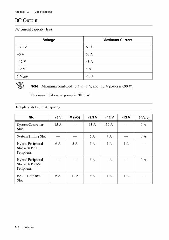
DC Output
DC current capacity (IMP)
Note Maximum combined +3.3 V, +5 V, and +12 V power is 699 W.
Maximum total usable power is 701.5 W.
Backplane slot current capacity
Voltage Maximum Current
+3.3 V 60 A
+5 V 50 A
+12 V 45 A
-12 V 4 A
5 VAUX 2.0 A
Slot +5 V V (I/O) +3.3 V +12 V -12 V 5 VAUX
System Controller Slot
15 A — 15 A 30 A — 1 A
System Timing Slot — — 6 A 4 A — 1 A
Hybrid Peripheral Slot with PXI-1 Peripheral
6 A 5 A 6 A 1 A 1 A —
Hybrid Peripheral Slot with PXI-5 Peripheral
— — 6 A 4 A — 1 A
PXI-1 Peripheral Slot
6 A 11 A 6 A 1 A 1 A —
© National Instruments | A-3
NI PXIe-1065 User Manual
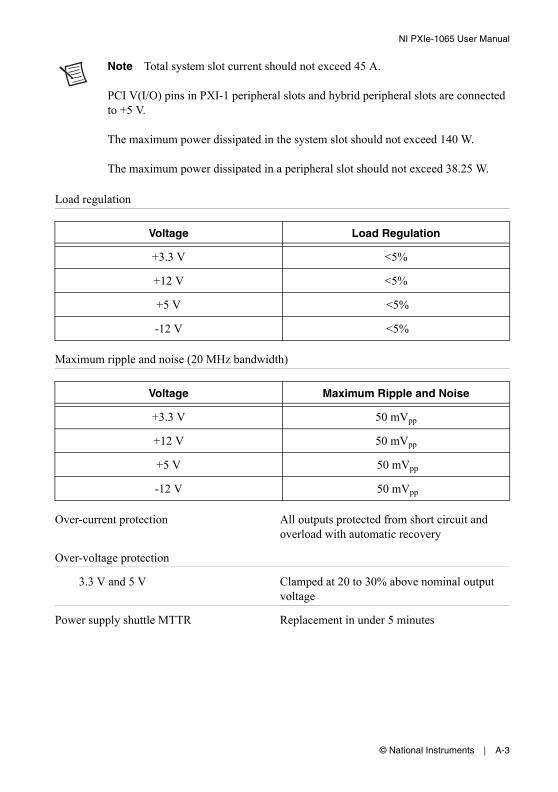
Note Total system slot current should not exceed 45 A.
PCI V(I/O) pins in PXI-1 peripheral slots and hybrid peripheral slots are connected to +5 V.
The maximum power dissipated in the system slot should not exceed 140 W.
The maximum power dissipated in a peripheral slot should not exceed 38.25 W.
Load regulation
Maximum ripple and noise (20 MHz bandwidth)
Over-current protection All outputs protected from short circuit and overload with automatic recovery
Over-voltage protection
3.3 V and 5 V Clamped at 20 to 30% above nominal output voltage
Power supply shuttle MTTR Replacement in under 5 minutes
Voltage Load Regulation
+3.3 V <5%
+12 V <5%
+5 V <5%
-12 V <5%
Voltage Maximum Ripple and Noise
+3.3 V 50 mVpp
+12 V 50 mVpp
+5 V 50 mVpp
-12 V 50 mVpp
A-4 | ni.com
Appendix A Specifications
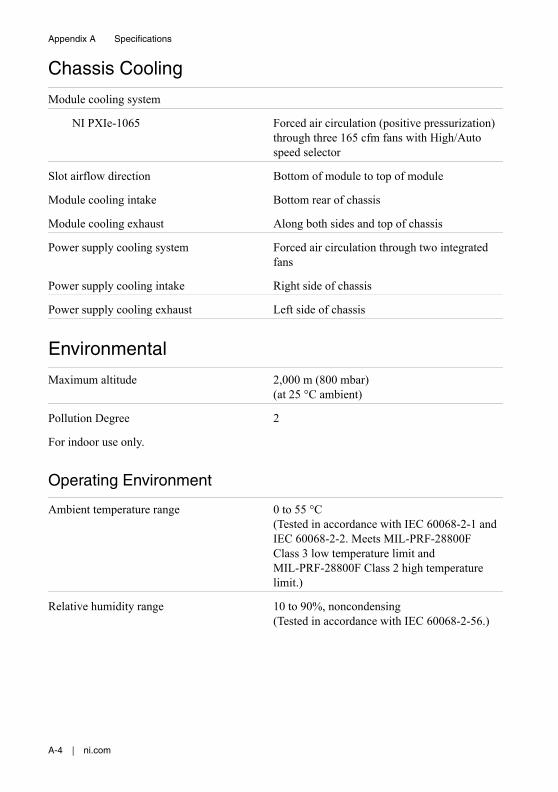
Chassis Cooling
Module cooling system
NI PXIe-1065 Forced air circulation (positive pressurization) through three 165 cfm fans with High/Auto speed selector
Slot airflow direction Bottom of module to top of module
Module cooling intake Bottom rear of chassis
Module cooling exhaust Along both sides and top of chassis
Power supply cooling system Forced air circulation through two integrated fans
Power supply cooling intake Right side of chassis
Power supply cooling exhaust Left side of chassis
Environmental
Maximum altitude 2,000 m (800 mbar) (at 25 °C ambient)
Pollution Degree 2
For indoor use only.
Operating Environment
Ambient temperature range 0 to 55 °C (Tested in accordance with IEC 60068-2-1 and IEC 60068-2-2. Meets MIL-PRF-28800F Class 3 low temperature limit and MIL-PRF-28800F Class 2 high temperature limit.)
Relative humidity range 10 to 90%, noncondensing (Tested in accordance with IEC 60068-2-56.)
© National Instruments | A-5
NI PXIe-1065 User Manual
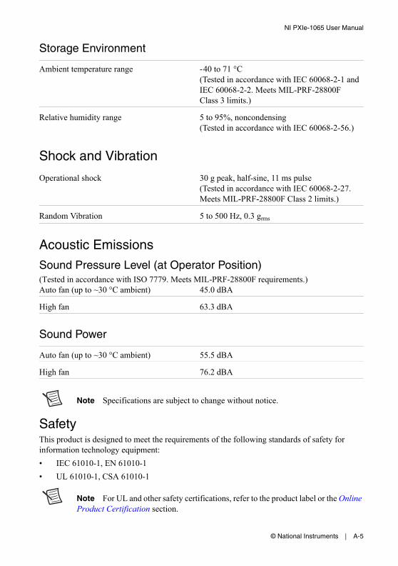
Storage Environment
Ambient temperature range -40 to 71 °C (Tested in accordance with IEC 60068-2-1 and IEC 60068-2-2. Meets MIL-PRF-28800F Class 3 limits.)
Relative humidity range 5 to 95%, noncondensing (Tested in accordance with IEC 60068-2-56.)
Shock and Vibration
Operational shock 30 g peak, half-sine, 11 ms pulse (Tested in accordance with IEC 60068-2-27. Meets MIL-PRF-28800F Class 2 limits.)
Random Vibration 5 to 500 Hz, 0.3 grms
Acoustic Emissions
Sound Pressure Level (at Operator Position)(Tested in accordance with ISO 7779. Meets MIL-PRF-28800F requirements.)Auto fan (up to ~30 °C ambient) 45.0 dBA
High fan 63.3 dBA
Sound Power
Auto fan (up to ~30 °C ambient) 55.5 dBA
High fan 76.2 dBA
Note Specifications are subject to change without notice.
SafetyThis product is designed to meet the requirements of the following standards of safety for information technology equipment:
• IEC 61010-1, EN 61010-1
• UL 61010-1, CSA 61010-1
Note For UL and other safety certifications, refer to the product label or the Online Product Certification section.

A-6 | ni.com
Appendix A Specifications
Electromagnetic CompatibilityThis product meets the requirements of the following EMC standards for electrical equipment for measurement, control, and laboratory use:
• EN 61326 (IEC 61326): Class A emissions; Basic immunity
• EN 55011 (CISPR 11): Group 1, Class A emissions
• AS/NZS CISPR 11: Group 1, Class A emissions
• FCC 47 CFR Part 15B: Class A emissions
• ICES-001: Class A emissions
Note For the standards applied to assess the EMC of this product, refer to the Online Product Certification section.
Note For EMC compliance, operate this device with shielded cabling.
CE ComplianceThis product meets the essential requirements of applicable European Directives as follows:
• 2006/95/EC; Low-Voltage Directive (safety)
• 2004/108/EC; Electromagnetic Compatibility Directive (EMC)
Online Product CertificationRefer to the product Declaration of Conformity (DoC) for additional regulatory compliance information. To obtain product certifications and the DoC for this product, visit ni.com/certification, search by model number or product line, and click the appropriate link in the Certification column.
Environmental ManagementNI is committed to designing and manufacturing products in an environmentally responsible manner. NI recognizes that eliminating certain hazardous substances from our products is beneficial to the environment and to NI customers.
For additional environmental information, refer to the Minimize Our Environmental Impact web page at ni.com/environment. This page contains the environmental regulations and directives with which NI complies, as well as other environmental information not included in this document.
Waste Electrical and Electronic Equipment (WEEE)EU Customers At the end of the product life cycle, all products must be sent to a WEEE recycling center. For more information about WEEE recycling centers, National Instruments WEEE initiatives, and compliance with WEEE Directive 2002/96/EC on Waste and Electronic Equipment, visit ni.com/environment/weee.
© National Instruments | A-7
NI PXIe-1065 User Manual
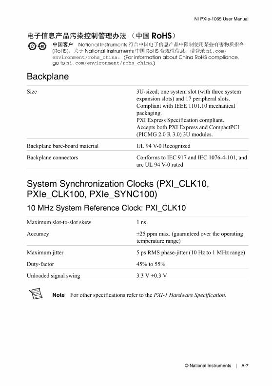
Backplane
Size 3U-sized; one system slot (with three system expansion slots) and 17 peripheral slots.Compliant with IEEE 1101.10 mechanical packaging.PXI Express Specification compliant.Accepts both PXI Express and CompactPCI (PICMG 2.0 R 3.0) 3U modules.
Backplane bare-board material UL 94 V-0 Recognized
Backplane connectors Conforms to IEC 917 and IEC 1076-4-101, and are UL 94 V-0 rated
System Synchronization Clocks (PXI_CLK10, PXIe_CLK100, PXIe_SYNC100)
10 MHz System Reference Clock: PXI_CLK10
Maximum slot-to-slot skew 1 ns
Accuracy ±25 ppm max. (guaranteed over the operating temperature range)
Maximum jitter 5 ps RMS phase-jitter (10 Hz to 1 MHz range)
Duty-factor 45% to 55%
Unloaded signal swing 3.3 V ±0.3 V
Note For other specifications refer to the PXI-1 Hardware Specification.
RoHSNational Instruments
(RoHS) National Instruments RoHS ni.com/environment/rohs_china (For information about China RoHS compliance, go to ni.com/environment/rohs_china.)
A-8 | ni.com
Appendix A Specifications
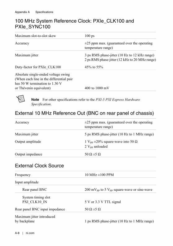
100 MHz System Reference Clock: PXIe_CLK100 and PXIe_SYNC100
Maximum slot-to-slot skew 100 ps
Accuracy ±25 ppm max. (guaranteed over the operating temperature range)
Maximum jitter 3 ps RMS phase-jitter (10 Hz to 12 kHz range)2 ps RMS phase-jitter (12 kHz to 20 MHz range)
Duty-factor for PXIe_CLK100 45% to 55%
Absolute single-ended voltage swing(When each line in the differential pairhas 50 W termination to 1.30 Vor Thévenin equivalent) 400 to 1000 mV
Note For other specifications refer to the PXI-5 PXI Express Hardware Specification.
External 10 MHz Reference Out (BNC on rear panel of chassis)
Accuracy ±25 ppm max. (guaranteed over the operating temperature range)
Maximum jitter 5 ps RMS phase-jitter (10 Hz to 1 MHz range)
Output amplitude 1 VPP ±20% square-wave into 50 Ω2 VPP unloaded
Output impedance 50 Ω ±5 Ω
External Clock Source
Frequency 10 MHz ±100 PPM
Input amplitude
Rear panel BNC 200 mVPP to 5 VPP square-wave or sine-wave
System timing slotPXI_CLK10_IN 5 V or 3.3 V TTL signal
Rear panel BNC input impedance 50 Ω ±5 Ω
Maximum jitter introducedby backplane 1 ps RMS phase-jitter (10 Hz to 1 MHz range)
© National Instruments | A-9
NI PXIe-1065 User Manual
PXIe_SYNC_CTRL
VIH 2.0 to 5.5 V
VIL 0 to 0.8 V
PXI Star Trigger
Maximum slot-to-slot skew 250 ps
Backplane characteristic impedance 65 Ω ±10%
Note For PXI slot to PXI Star mapping refer to the System Timing Slot section of Chapter 1, Getting Started.
For other specifications refer to the PXI-1 Hardware Specification.
PXI Differential Star Triggers (PXIe-DSTARA, PXIe-DSTARB, PXIe-DSTARC)
Maximum slot-to-slot skew 150 ps
Maximum differential skew 25 ps
Backplane differential impedance 100 Ω ±10%
Note For PXIe slot to PXI_DSTAR mapping refer to the System Timing Slot section of Chapter 1, Getting Started.
For other specifications, the NI PXIe-1065 complies with the PXI-5 PXI Express Hardware Specification.
Mechanical
Overall dimensions
Standard chassis
Height 6.97 in. (177.1 mm)
Width 18.30 in. (464.8 mm)
Depth 18.40 in. (467.4 mm)
A-10 | ni.com
Appendix A Specifications
Note 0.57 in. (14.5 mm) is added to height when feet are installed. When tilted with front feet extended on table top, height is increased approximately 2.08 in. (52.8 mm) in front and 0.583 in. (14.8 mm) in rear.
Weight 12.8 kg (28.2 lb)
Chassis materials Sheet Aluminum (5052-H32, 3003-H14, and 6061-T6), Extruded Aluminum (6060-T6), and Cold Rolled Steel, PC-ABS, Santoprene, Nylon
Finish Conductive Clear Iridite on AluminumElectroplated Nickel on Cold Rolled SteelPolyurethane Enamel
© National Instruments | A-11
NI PXIe-1065 User Manual
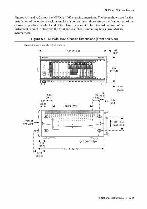
Figures A-1 and A-2 show the NI PXIe-1065 chassis dimensions. The holes shown are for the installation of the optional rack mount kits. You can install those kits on the front or rear of the chassis, depending on which end of the chassis you want to face toward the front of the instrument cabinet. Notice that the front and rear chassis mounting holes (size M4) are symmetrical.
Figure A-1. NI PXIe-1065 Chassis Dimensions (Front and Side)
0.57(14.5)
Dimensions are in inches (millimeters)
0.30 (7.25)
.39(9.9)
17.54 (445.6)
6.97(177.1)
3.54(90.0)
1.84(46.8)
17.11 (434.6)
3.19(81.1)
2.12(53.8)
1.58(40.1)
1.14(29.1)
1.37(34.8)
10.21 (259.1)
181716151312111098765432
NI PXIe-1065
1H
14H H H
1.82(46.3)
1.82(46.3)
Front ofPXI Card
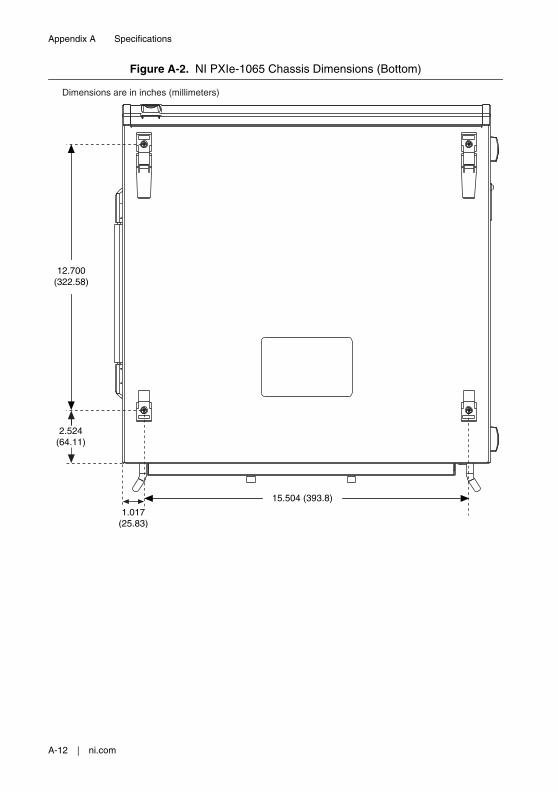
A-12 | ni.com
Appendix A Specifications
Figure A-2. NI PXIe-1065 Chassis Dimensions (Bottom)
1.017(25.83)
2.524(64.11)
15.504 (393.8)
12.700(322.58)
Dimensions are in inches (millimeters)
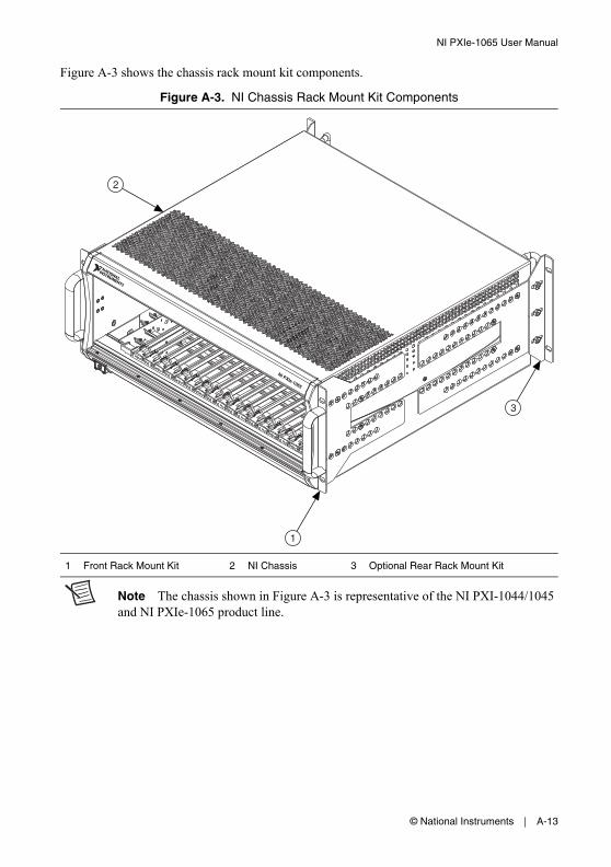
© National Instruments | A-13
NI PXIe-1065 User Manual
Figure A-3 shows the chassis rack mount kit components.
Figure A-3. NI Chassis Rack Mount Kit Components
Note The chassis shown in Figure A-3 is representative of the NI PXI-1044/1045 and NI PXIe-1065 product line.
1 Front Rack Mount Kit 2 NI Chassis 3 Optional Rear Rack Mount Kit
3
NI PXIe-1065
2
1
© National Instruments | B-1
BPinouts
This appendix describes the connector pinouts for the NI PXIe-1065 chassis backplane.
Table B-1 shows the XP1 connector pinout for the System Controller slot.
Table B-2 shows the XP2 Connector Pinout for the System Controller slot.
Table B-3 shows the XP3 Connector Pinout for the System Controller slot.
Table B-4 shows the XP4 Connector Pinout for the System Controller slot.
Table B-5 shows the TP1 Connector Pinout for the System Controller slot.
Table B-6 shows the TP2 Connector Pinout for the System Timing slot.
Table B-7 shows the XP3 Connector Pinout for the System Timing slot.
Table B-8 shows the XP4 Connector Pinout for the System Timing slot.
Table B-9 shows the P1 connector pinout for the peripheral slots.
Table B-10 shows the P2 connector pinout for the peripheral slots.
Table B-11 shows the P1 connector pinout for the Hybrid peripheral slots.
Table B-12 shows the XP3 Connector Pinout for the Hybrid peripheral slots.
Table B-13 shows the XP4 Connector Pinout for the Hybrid peripheral slots.
For more detailed information, refer to the PXI-5 PXI Express Hardware Specification, Revision 2.0. Contact the PXI Systems Alliance for a copy of the specification.
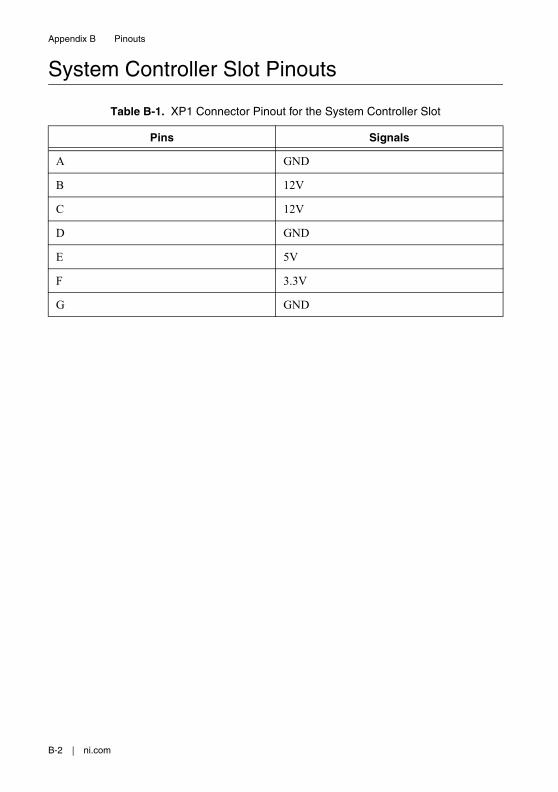
B-2 | ni.com
Appendix B Pinouts
System Controller Slot Pinouts
Table B-1. XP1 Connector Pinout for the System Controller Slot
Pins Signals
A GND
B 12V
C 12V
D GND
E 5V
F 3.3V
G GND
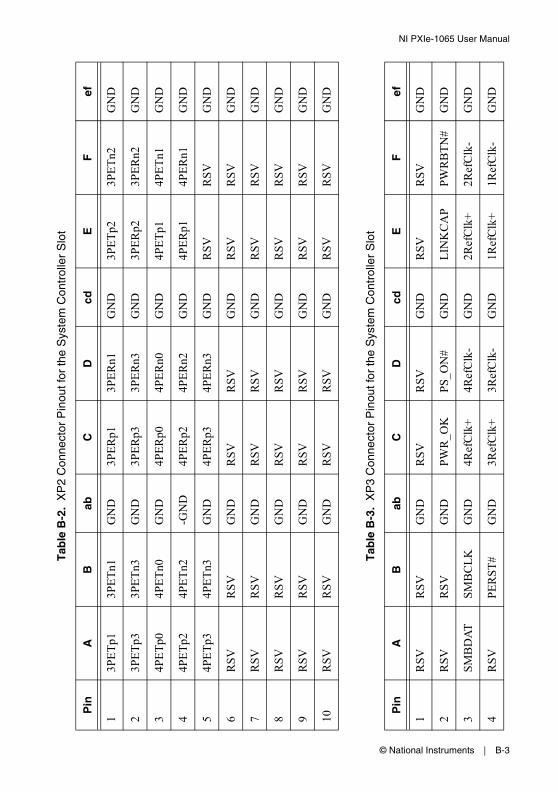
NI PXIe-1065 User Manual
© National Instruments | B-3
Tab
le B
-2.
XP
2 C
onne
ctor
Pin
out f
or th
e S
yste
m C
ontr
olle
r S
lot
Pin
AB
abC
Dcd
EF
ef
13P
ET
p13P
ET
n1G
ND
3PE
Rp1
3PE
Rn1
GN
D3P
ET
p23P
ET
n2G
ND
23P
ET
p33P
ET
n3G
ND
3PE
Rp3
3PE
Rn3
GN
D3P
ER
p23P
ER
n2G
ND
34P
ET
p04P
ET
n0G
ND
4PE
Rp0
4PE
Rn0
GN
D4P
ET
p14P
ET
n1G
ND
44P
ET
p24P
ET
n2-G
ND
4PE
Rp2
4PE
Rn2
GN
D4P
ER
p14P
ER
n1G
ND
54P
ET
p34P
ET
n3G
ND
4PE
Rp3
4PE
Rn3
GN
DR
SV
RS
VG
ND
6R
SV
RS
VG
ND
RS
VR
SV
GN
DR
SV
RS
VG
ND
7R
SV
RS
VG
ND
RS
VR
SV
GN
DR
SV
RS
VG
ND
8R
SV
RS
VG
ND
RS
VR
SV
GN
DR
SV
RS
VG
ND
9R
SV
RS
VG
ND
RS
VR
SV
GN
DR
SV
RS
VG
ND
10R
SV
RS
VG
ND
RS
VR
SV
GN
DR
SV
RS
VG
ND
Tab
le B
-3.
XP
3 C
onne
ctor
Pin
out f
or th
e S
yste
m C
ontr
olle
r S
lot
Pin
AB
abC
Dcd
EF
ef
1R
SV
RS
VG
ND
RS
VR
SV
GN
DR
SV
RS
VG
ND
2R
SV
RS
VG
ND
PW
R_O
KP
S_O
N#
GN
DL
INK
CA
PPW
RB
TN
#G
ND
3S
MB
DA
TS
MB
CL
KG
ND
4Ref
Clk
+4R
efC
lk-
GN
D2R
efC
lk+
2Ref
Clk
-G
ND
4R
SV
PE
RST
#G
ND
3Ref
Clk
+3R
efC
lk-
GN
D1R
efC
lk+
1Ref
Clk
-G
ND
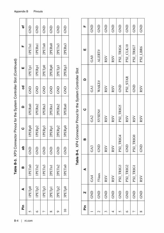
Appendix B Pinouts
B-4 | ni.com
51P
ET
p01P
ET
n0G
ND
1PE
Rp0
1PE
Rn0
GN
D1P
ET
p11P
ET
n1G
ND
61P
ET
p21P
ET
n2G
ND
1PE
Rp2
1PE
Rn2
GN
D1P
ER
p11P
ER
n1G
ND
71P
ET
p31P
ET
n3G
ND
1PE
Rp3
1PE
Rn3
GN
D2P
ET
p02P
ET
n0G
ND
82P
ET
p12P
ET
n1G
ND
2PE
Rp1
2PE
Rn1
GN
D2P
ER
p02P
ER
n0G
ND
92P
ET
p22P
ET
n2G
ND
2PE
Rp2
2PE
Rn2
GN
D2P
ET
p32P
ET
n3G
ND
103P
ET
p03P
ET
n0G
ND
3PE
Rp0
3PE
Rn0
GN
D2P
ER
p32P
ER
n3G
ND
Tab
le B
-4.
XP
4 C
onne
ctor
Pin
out f
or th
e S
yste
m C
ontr
olle
r S
lot
Pin
ZA
BC
DE
F
1G
ND
GA
4G
A3
GA
2G
A1
GA
0G
ND
2G
ND
5Vau
xG
ND
SYSE
N#
WA
KE
#A
LE
RT
#G
ND
3G
ND
RS
VR
SV
RS
VR
SV
RS
VG
ND
4G
ND
RS
VR
SV
RS
VR
SV
RS
VG
ND
5G
ND
PXI_
TR
IG3
PX
I_T
RIG
4P
XI_
TR
IG5
GN
DP
XI_
TR
IG6
GN
D
6G
ND
PXI_
TR
IG2
GN
DR
SV
PX
I_S
TAR
PX
I_C
LK
10G
ND
7G
ND
PXI_
TR
IG1
PX
I_T
RIG
0R
SV
GN
DP
XI_
TR
IG7
GN
D
8G
ND
RS
VG
ND
RS
VR
SV
PX
I_L
BR
6G
ND
Tab
le B
-3.
XP
3 C
onne
ctor
Pin
out f
or th
e S
yste
m C
ontr
olle
r S
lot (
Con
tinue
d)
Pin
AB
abC
Dcd
EF
ef
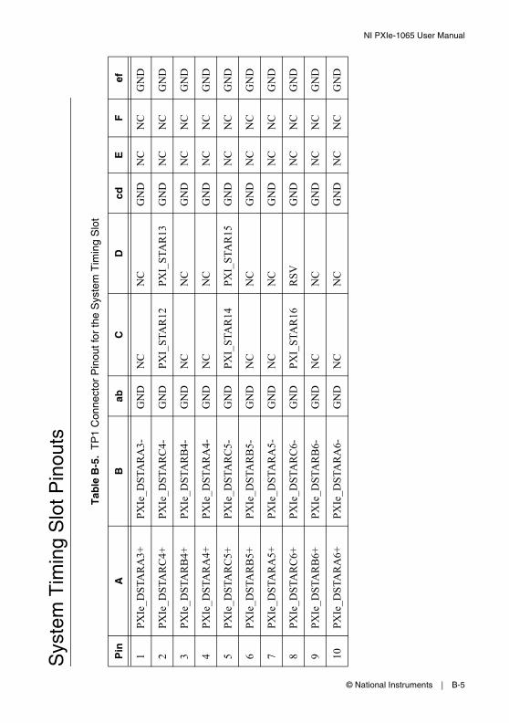
NI PXIe-1065 User Manual
© National Instruments | B-5
Sys
tem
Tim
ing
Slo
t Pin
outs
Tab
le B
-5.
TP
1 C
onne
ctor
Pin
out f
or th
e S
yste
m T
imin
g S
lot
Pin
AB
abC
Dcd
EF
ef
1P
XIe
_DS
TAR
A3+
PXIe
_DST
AR
A3-
GN
DN
CN
CG
ND
NC
NC
GN
D
2P
XIe
_DS
TAR
C4+
PX
Ie_D
STA
RC
4-G
ND
PX
I_S
TAR
12P
XI_
STA
R13
GN
DN
CN
CG
ND
3P
XIe
_DS
TAR
B4+
PX
Ie_D
STA
RB
4-G
ND
NC
NC
GN
DN
CN
CG
ND
4P
XIe
_DS
TAR
A4+
PXIe
_DST
AR
A4-
GN
DN
CN
CG
ND
NC
NC
GN
D
5P
XIe
_DS
TAR
C5+
PX
Ie_D
STA
RC
5-G
ND
PX
I_S
TAR
14P
XI_
STA
R15
GN
DN
CN
CG
ND
6P
XIe
_DS
TAR
B5+
PX
Ie_D
STA
RB
5-G
ND
NC
NC
GN
DN
CN
CG
ND
7P
XIe
_DS
TAR
A5+
PXIe
_DST
AR
A5-
GN
DN
CN
CG
ND
NC
NC
GN
D
8P
XIe
_DS
TAR
C6+
PX
Ie_D
STA
RC
6-G
ND
PX
I_S
TAR
16R
SV
GN
DN
CN
CG
ND
9P
XIe
_DS
TAR
B6+
PX
Ie_D
STA
RB
6-G
ND
NC
NC
GN
DN
CN
CG
ND
10P
XIe
_DS
TAR
A6+
PXIe
_DST
AR
A6-
GN
DN
CN
CG
ND
NC
NC
GN
D
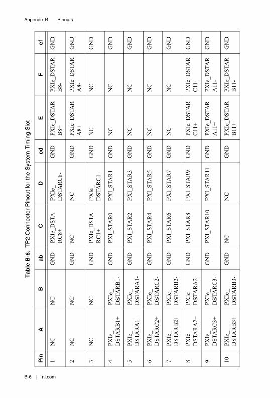
Appendix B Pinouts
B-6 | ni.com
Tab
le B
-6.
TP
2 C
onne
ctor
Pin
out f
or th
e S
yste
m T
imin
g S
lot
Pin
AB
abC
Dcd
EF
ef
1N
CN
CG
ND
PX
Ie_D
STA
RC
8+P
XIe
_D
STA
RC
8-G
ND
PX
Ie_D
STA
RB
8+PX
Ie_D
STA
RB
8-G
ND
2N
CN
CG
ND
NC
NC
GN
DP
XIe
_DS
TAR
A8+
PXIe
_DST
AR
A8-
GN
D
3N
CN
CG
ND
PX
Ie_D
STA
RC
1+P
XIe
_D
STA
RC
1-G
ND
NC
NC
GN
D
4PX
Ie_
DS
TAR
B1+
PX
Ie_
DS
TAR
B1-
GN
DP
XI_
STA
R0
PX
I_S
TAR
1G
ND
NC
NC
GN
D
5PX
Ie_
DS
TAR
A1+
PX
Ie_
DS
TAR
A1-
GN
DP
XI_
STA
R2
PX
I_S
TAR
3G
ND
NC
NC
GN
D
6PX
Ie_
DS
TAR
C2+
PX
Ie_
DS
TAR
C2-
GN
DP
XI_
STA
R4
PX
I_S
TAR
5G
ND
NC
NC
GN
D
7PX
Ie_
DS
TAR
B2+
PX
Ie_
DS
TAR
B2-
GN
DP
XI_
STA
R6
PX
I_S
TAR
7G
ND
NC
NC
GN
D
8PX
Ie_
DS
TAR
A2+
PX
Ie_
DS
TAR
A2-
GN
DP
XI_
STA
R8
PX
I_S
TAR
9G
ND
PX
Ie_D
STA
RC
11+
PXIe
_DST
AR
C11
-G
ND
9PX
Ie_
DS
TAR
C3+
PX
Ie_
DS
TAR
C3-
GN
DP
XI_
STA
R10
PX
I_S
TAR
11G
ND
PX
Ie_D
STA
RA
11+
PXIe
_DST
AR
A11
-G
ND
10PX
Ie_
DS
TAR
B3+
PX
Ie_
DS
TAR
B3-
GN
DN
CN
CG
ND
PX
Ie_D
STA
RB
11+
PXIe
_DST
AR
B11
-G
ND
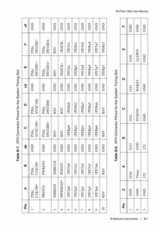
NI PXIe-1065 User Manual
© National Instruments | B-7
Tab
le B
-7.
XP
3 C
onne
ctor
Pin
out f
or th
e S
yste
m T
imin
g S
lot
Pin
AB
abC
Dcd
EF
ef
1P
XIe
_C
LK
100+
PX
Ie_
CL
K10
0-G
ND
PX
Ie_
SY
NC
100+
PX
Ie_
SY
NC
100-
GN
DP
XIe
_D
STA
RC
+P
XIe
_D
STA
RC
-G
ND
2P
RS
NT
#P
WR
EN
#G
ND
PX
Ie_
DS
TAR
B+
PX
Ie_
DS
TAR
B-
GN
DP
XIe
_D
STA
RA
+P
XIe
_D
STA
RA
-G
ND
3S
MB
DA
TS
MB
CL
KG
ND
RS
VR
SV
GN
DR
SV
RS
VG
ND
4M
PWR
GD
*P
ER
ST#
GN
DR
SV
RS
VG
ND
1Ref
Clk
+1R
efC
lk-
GN
D
51P
ET
p01P
ET
n0G
ND
1PE
Rp0
1PE
Rn0
GN
D1P
ET
p11P
ET
n1G
ND
61P
ET
p21P
ET
n2G
ND
1PE
Rp2
1PE
Rn2
GN
D1P
ER
p11P
ER
n1G
ND
71P
ET
p31P
ET
n3G
ND
1PE
Rp3
1PE
Rn3
GN
D1P
ET
p41P
ET
n4G
ND
81P
ET
p51P
ET
n5G
ND
1PE
Rp5
1PE
Rn5
GN
D1P
ER
p41P
ER
n4G
ND
91P
ET
p61P
ET
n6G
ND
1PE
Rp6
1PE
Rn6
GN
D1P
ET
p71P
ET
n7G
ND
10R
SV
RS
VG
ND
RS
VR
SV
GN
D1P
ER
p71P
ER
n7G
ND
Tab
le B
-8.
XP
4 C
onne
ctor
Pin
out f
or th
e S
yste
m T
imin
g S
lot
Pin
ZA
BC
DE
F
1G
ND
GA
4G
A3
GA
2G
A1
GA
0G
ND
2G
ND
5Vau
xG
ND
SYSE
N#
WA
KE
#A
LE
RT
#G
ND
3G
ND
12V
12V
GN
DG
ND
GN
DG
ND
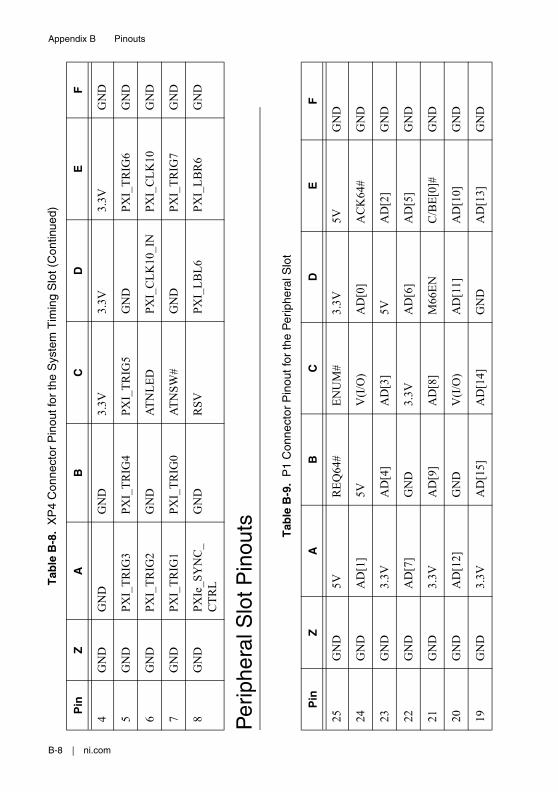
Appendix B Pinouts
B-8 | ni.com
Per
iphe
ral S
lot P
inou
ts
4G
ND
GN
DG
ND
3.3V
3.3V
3.3V
GN
D
5G
ND
PX
I_T
RIG
3P
XI_
TR
IG4
PX
I_T
RIG
5G
ND
PX
I_T
RIG
6G
ND
6G
ND
PX
I_T
RIG
2G
ND
AT
NL
ED
PX
I_C
LK
10_I
NP
XI_
CL
K10
GN
D
7G
ND
PX
I_T
RIG
1P
XI_
TR
IG0
AT
NS
W#
GN
DP
XI_
TR
IG7
GN
D
8G
ND
PX
Ie_S
YN
C_
CT
RL
GN
DR
SV
PX
I_L
BL
6P
XI_
LB
R6
GN
D
Tab
le B
-9.
P1
Con
nect
or P
inou
t for
the
Per
iphe
ral S
lot
Pin
ZA
BC
DE
F
25G
ND
5VR
EQ
64#
EN
UM
#3.
3V5V
GN
D
24G
ND
AD
[1]
5VV
(I/O
)A
D[0
]A
CK
64#
GN
D
23G
ND
3.3V
AD
[4]
AD
[3]
5VA
D[2
]G
ND
22G
ND
AD
[7]
GN
D3.
3VA
D[6
]A
D[5
]G
ND
21G
ND
3.3V
AD
[9]
AD
[8]
M66
EN
C/B
E[0
]#G
ND
20G
ND
AD
[12]
GN
DV
(I/O
)A
D[1
1]A
D[1
0]G
ND
19G
ND
3.3V
AD
[15]
AD
[14]
GN
DA
D[1
3]G
ND
Tab
le B
-8.
XP
4 C
onne
ctor
Pin
out f
or th
e S
yste
m T
imin
g S
lot (
Con
tinue
d)
Pin
ZA
BC
DE
F
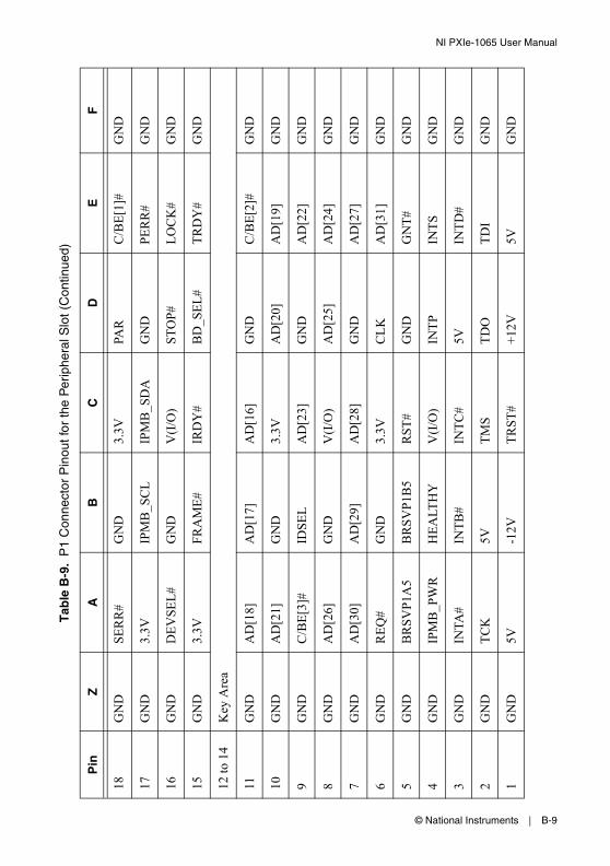
NI PXIe-1065 User Manual
© National Instruments | B-9
18G
ND
SE
RR
#G
ND
3.3V
PAR
C/B
E[1
]#G
ND
17G
ND
3.3V
IPM
B_S
CL
IPM
B_S
DA
GN
DP
ER
R#
GN
D
16G
ND
DE
VS
EL
#G
ND
V(I
/O)
STO
P#
LO
CK
#G
ND
15G
ND
3.3V
FR
AM
E#
IRD
Y#
BD
_SE
L#
TR
DY
#G
ND
12 to
14
Key
Are
a
11G
ND
AD
[18]
AD
[17]
AD
[16]
GN
DC
/BE
[2]#
GN
D
10G
ND
AD
[21]
GN
D3.
3VA
D[2
0]A
D[1
9]G
ND
9G
ND
C/B
E[3
]#ID
SE
LA
D[2
3]G
ND
AD
[22]
GN
D
8G
ND
AD
[26]
GN
DV
(I/O
)A
D[2
5]A
D[2
4]G
ND
7G
ND
AD
[30]
AD
[29]
AD
[28]
GN
DA
D[2
7]G
ND
6G
ND
RE
Q#
GN
D3.
3VC
LK
AD
[31]
GN
D
5G
ND
BR
SV
P1A
5B
RS
VP
1B5
RST
#G
ND
GN
T#
GN
D
4G
ND
IPM
B_P
WR
HE
ALT
HY
V(I
/O)
INT
PIN
TS
GN
D
3G
ND
INTA
#IN
TB
#IN
TC
#5V
INT
D#
GN
D
2G
ND
TC
K5V
TM
ST
DO
TD
IG
ND
1G
ND
5V-1
2VT
RST
#+
12V
5VG
ND
Tab
le B
-9.
P1
Con
nect
or P
inou
t for
the
Per
iphe
ral S
lot (
Con
tinue
d)
Pin
ZA
BC
DE
F
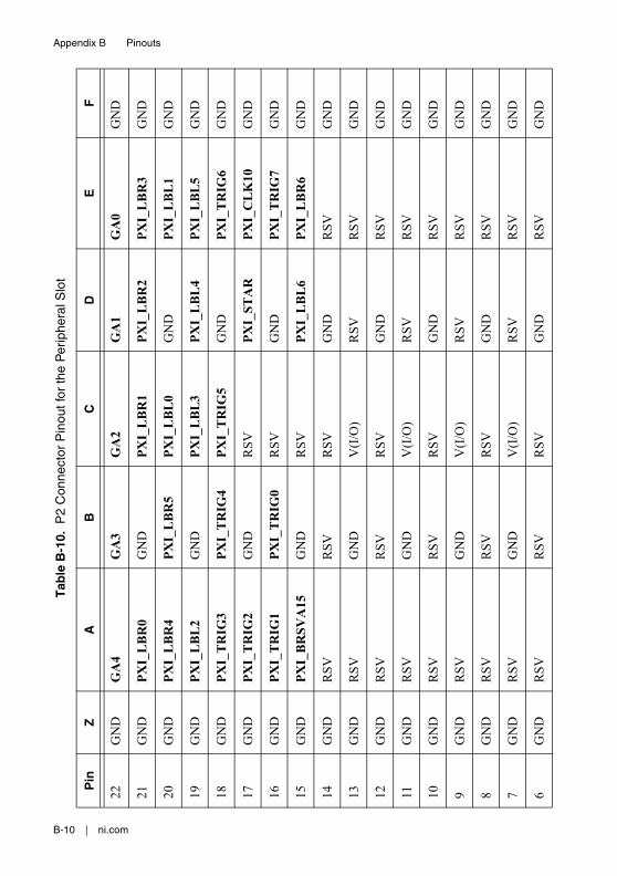
Appendix B Pinouts
B-10 | ni.com
Tab
le B
-10.
P2
Con
nect
or P
inou
t for
the
Per
iphe
ral S
lot
Pin
ZA
BC
DE
F
22G
ND
GA
4G
A3
GA
2G
A1
GA
0G
ND
21G
ND
PXI_
LB
R0
GN
DPX
I_L
BR
1PX
I_L
BR
2PX
I_L
BR
3G
ND
20G
ND
PXI_
LB
R4
PXI_
LB
R5
PXI_
LB
L0
GN
DPX
I_L
BL1
GN
D
19G
ND
PXI_
LB
L2
GN
DPX
I_L
BL
3PX
I_L
BL
4PX
I_L
BL5
GN
D
18G
ND
PXI_
TR
IG3
PXI_
TR
IG4
PXI_
TR
IG5
GN
DPX
I_T
RIG
6G
ND
17G
ND
PXI_
TR
IG2
GN
DR
SV
PXI_
STA
RPX
I_C
LK
10G
ND
16G
ND
PXI_
TR
IG1
PXI_
TR
IG0
RS
VG
ND
PXI_
TR
IG7
GN
D
15G
ND
PXI_
BR
SVA
15G
ND
RS
VPX
I_L
BL
6PX
I_L
BR
6G
ND
14G
ND
RS
VR
SV
RS
VG
ND
RS
VG
ND
13G
ND
RS
VG
ND
V(I
/O)
RS
VR
SV
GN
D
12G
ND
RS
VR
SV
RS
VG
ND
RS
VG
ND
11G
ND
RS
VG
ND
V(I
/O)
RS
VR
SV
GN
D
10G
ND
RS
VR
SV
RS
VG
ND
RS
VG
ND
9G
ND
RS
VG
ND
V(I
/O)
RS
VR
SV
GN
D
8G
ND
RS
VR
SV
RS
VG
ND
RS
VG
ND
7G
ND
RS
VG
ND
V(I
/O)
RS
VR
SV
GN
D
6G
ND
RS
VR
SV
RS
VG
ND
RS
VG
ND
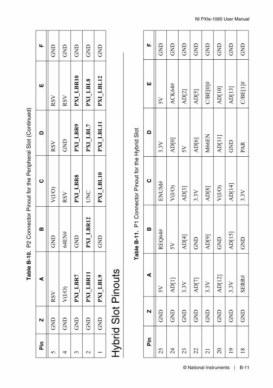
NI PXIe-1065 User Manual
© National Instruments | B-11
Hyb
rid S
lot P
inou
ts
5G
ND
RS
VG
ND
V(I
/O)
RS
VR
SV
GN
D
4G
ND
V(I
/O)
64E
N#
RS
VG
ND
RS
VG
ND
3G
ND
PXI_
LB
R7
GN
DPX
I_L
BR
8PX
I_L
BR
9PX
I_L
BR
10G
ND
2G
ND
PXI_
LB
R11
PXI_
LB
R12
UN
CPX
I_L
BL
7PX
I_L
BL8
GN
D
1G
ND
PXI_
LB
L9
GN
DPX
I_L
BL
10PX
I_L
BL
11PX
I_L
BL12
GN
D
Tab
le B
-11.
P1
Con
nect
or P
inou
t for
the
Hyb
rid S
lot
Pin
ZA
BC
DE
F
25G
ND
5VR
EQ
64#
EN
UM
#3.
3V5V
GN
D
24G
ND
AD
[1]
5VV
(I/O
)A
D[0
]A
CK
64#
GN
D
23G
ND
3.3V
AD
[4]
AD
[3]
5VA
D[2
]G
ND
22G
ND
AD
[7]
GN
D3.
3VA
D[6
]A
D[5
]G
ND
21G
ND
3.3V
AD
[9]
AD
[8]
M66
EN
C/B
E[0
]#G
ND
20G
ND
AD
[12]
GN
DV
(I/O
)A
D[1
1]A
D[1
0]G
ND
19G
ND
3.3V
AD
[15]
AD
[14]
GN
DA
D[1
3]G
ND
18G
ND
SE
RR
#G
ND
3.3V
PAR
C/B
E[1
]#G
ND
Tab
le B
-10.
P2
Con
nect
or P
inou
t for
the
Per
iphe
ral S
lot (
Con
tinue
d)
Pin
ZA
BC
DE
F
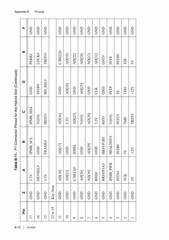
Appendix B Pinouts
B-12 | ni.com
17G
ND
3.3V
IPM
B_S
CL
IPM
B_S
DA
GN
DP
ER
R#
GN
D
16G
ND
DE
VS
EL
#G
ND
V(I
/O)
STO
P#
LO
CK
#G
ND
15G
ND
3.3V
FR
AM
E#
IRD
Y#
BD
_SE
L#
TR
DY
#G
ND
12 to
14
Key
Are
a
11G
ND
AD
[18]
AD
[17]
AD
[16]
GN
DC
/BE
[2]#
GN
D
10G
ND
AD
[21]
GN
D3.
3VA
D[2
0]A
D[1
9]G
ND
9G
ND
C/B
E[3
]#ID
SE
LA
D[2
3]G
ND
AD
[22]
GN
D
8G
ND
AD
[26]
GN
DV
(I/O
)A
D[2
5]A
D[2
4]G
ND
7G
ND
AD
[30]
AD
[29]
AD
[28]
GN
DA
D[2
7]G
ND
6G
ND
RE
Q#
GN
D3.
3VC
LK
AD
[31]
GN
D
5G
ND
BR
SV
P1A
5B
RS
VP
1B5
RST
#G
ND
GN
T#
GN
D
4G
ND
IPM
B_P
WR
HE
ALT
HY
#V
(I/O
)IN
TP
INT
SG
ND
3G
ND
INTA
#IN
TB
#IN
TC
#5V
INT
D#
GN
D
2G
ND
TC
K5V
TM
ST
DO
TD
IG
ND
1G
ND
5V-1
2VT
RST
#+
12V
5VG
ND
Tab
le B
-11.
P1
Con
nect
or P
inou
t for
the
Hyb
rid S
lot (
Con
tinue
d)
Pin
ZA
BC
DE
F
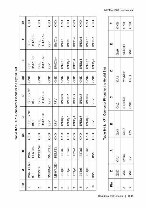
NI PXIe-1065 User Manual
© National Instruments | B-13
Tab
le B
-12.
XP
3 C
onne
ctor
Pin
out f
or th
e H
ybrid
Slo
t
Pin
AB
abC
Dcd
EF
ef
1P
XIe
_CL
K1
00+
PX
Ie_
CL
K10
0-G
ND
PX
Ie_S
YN
C10
0+P
XIe
_SY
NC
100-
GN
DP
XIe
_D
STA
RC
+P
XIe
_D
STA
RC
-G
ND
2P
RS
NT
#P
WR
EN
#G
ND
PX
Ie_
DST
AR
B+
PX
Ie_
DST
AR
B-
GN
DP
XIe
_D
STA
RA
+P
XIe
_D
STA
RA
-G
ND
3S
MB
DA
TS
MB
CL
KG
ND
RS
VR
SV
GN
DR
SV
RS
VG
ND
4M
PW
RG
D*
PER
ST#
GN
DR
SV
RS
VG
ND
1Ref
Clk
+1R
efC
lk-
GN
D
51P
ET
p01P
ET
n0G
ND
1PE
Rp0
1PE
Rn0
GN
D1P
ET
p11P
ET
n1G
ND
61P
ET
p21P
ET
n2G
ND
1PE
Rp2
1PE
Rn2
GN
D1P
ER
p11P
ER
n1G
ND
71P
ET
p31P
ET
n3G
ND
1PE
Rp3
1PE
Rn3
GN
D1P
ET
p41P
ET
n4G
ND
81P
ET
p51P
ET
n5G
ND
1PE
Rp5
1PE
Rn5
GN
D1P
ER
p41P
ER
n4G
ND
91P
ET
p61P
ET
n6G
ND
1PE
Rp6
1PE
Rn6
GN
D1P
ET
p71P
ET
n7G
ND
10R
SV
RS
VG
ND
RS
VR
SV
GN
D1P
ER
p71P
ER
n7G
ND
Tab
le B
-13.
XP
4 C
onne
ctor
Pin
out f
or th
e H
ybrid
Slo
t
Pin
ZA
BC
DE
F
1G
ND
GA
4G
A3
GA
2G
A1
GA
0G
ND
2G
ND
5Vau
xG
ND
SYSE
N#
WA
KE
#A
LE
RT
#G
ND
3G
ND
12V
12V
GN
DG
ND
GN
DG
ND
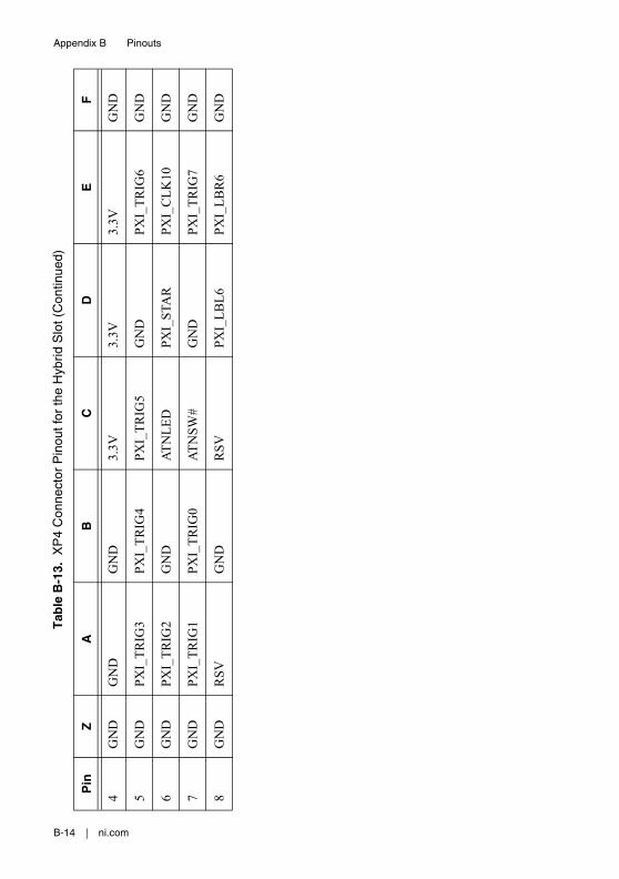
Appendix B Pinouts
B-14 | ni.com
4G
ND
GN
DG
ND
3.3V
3.3V
3.3V
GN
D
5G
ND
PXI_
TR
IG3
PX
I_T
RIG
4P
XI_
TR
IG5
GN
DP
XI_
TR
IG6
GN
D
6G
ND
PXI_
TR
IG2
GN
DA
TN
LE
DP
XI_
STA
RP
XI_
CL
K10
GN
D
7G
ND
PXI_
TR
IG1
PX
I_T
RIG
0A
TN
SW#
GN
DP
XI_
TR
IG7
GN
D
8G
ND
RS
VG
ND
RS
VP
XI_
LB
L6
PX
I_L
BR
6G
ND
Tab
le B
-13.
XP
4 C
onne
ctor
Pin
out f
or th
e H
ybrid
Slo
t (C
ontin
ued)
Pin
ZA
BC
DE
F
© National Instruments | C-1
CNI Services
NI provides global services and support as part of our commitment to your success. Take advantage of product services in addition to training and certification programs that meet your needs during each phase of the application life cycle; from planning and development through deployment and ongoing maintenance.
To get started, register your product at ni.com/myproducts.
As a registered NI product user, you are entitled to the following benefits:
• Access to applicable product services.
• Easier product management with an online account.
• Receive critical part notifications, software updates, and service expirations.
Log in to your MyNI user profile to get personalized access to your services.
Services and Resources
• Maintenance and Hardware Services—NI helps you identify your systems’ accuracy and reliability requirements and provides warranty, sparing, and calibration services to help you maintain accuracy and minimize downtime over the life of your system. Visit ni.com/services for more information.
– Warranty and Repair—All NI hardware features a one-year standard warranty that is extendable up to five years. NI offers repair services performed in a timely manner by highly trained factory technicians using only original parts at an NI service center.
– Calibration—Through regular calibration, you can quantify and improve the measurement performance of an instrument. NI provides state-of-the-art calibration services. If your product supports calibration, you can obtain the calibration certificate for your product at ni.com/calibration.
• System Integration—If you have time constraints, limited in-house technical resources, or other project challenges, National Instruments Alliance Partner members can help. To learn more, call your local NI office or visit ni.com/alliance.
C-2 | ni.com
Appendix C NI Services
• Training and Certification—The NI training and certification program is the most effective way to increase application development proficiency and productivity. Visit ni.com/training for more information.
– The Skills Guide assists you in identifying the proficiency requirements of your current application and gives you options for obtaining those skills consistent with your time and budget constraints and personal learning preferences. Visit ni.com/skills-guide to see these custom paths.
– NI offers courses in several languages and formats including instructor-led classes at facilities worldwide, courses on-site at your facility, and online courses to serve your individual needs.
• Technical Support—Support at ni.com/support includes the following resources:
– Self-Help Technical Resources—Visit ni.com/support for software drivers and updates, a searchable KnowledgeBase, product manuals, step-by-step troubleshooting wizards, thousands of example programs, tutorials, application notes, instrument drivers, and so on. Registered users also receive access to the NI Discussion Forums at ni.com/forums. NI Applications Engineers make sure every question submitted online receives an answer.
– Software Support Service Membership—The Standard Service Program (SSP) is a renewable one-year subscription included with almost every NI software product, including NI Developer Suite. This program entitles members to direct access to NI Applications Engineers through phone and email for one-to-one technical support, as well as exclusive access to online training modules at ni.com/self-paced-training. NI also offers flexible extended contract options that guarantee your SSP benefits are available without interruption for as long as you need them. Visit ni.com/ssp for more information.
• Declaration of Conformity (DoC)—A DoC is our claim of compliance with the Council of the European Communities using the manufacturer’s declaration of conformity. This system affords the user protection for electromagnetic compatibility (EMC) and product safety. You can obtain the DoC for your product by visiting ni.com/certification.
For information about other technical support options in your area, visit ni.com/services, or contact your local office at ni.com/contact.
You also can visit the Worldwide Offices section of ni.com/niglobal to access the branch office websites, which provide up-to-date contact information, support phone numbers, email addresses, and current events.
© National Instruments | G-1
Glossary
Symbol Prefix Value
p pico 10-12
n nano 10-9
μ micro 10-6
m milli 10-3
k kilo 103
M mega 106
G giga 109
T tera 1012
Symbols
° Degrees.
≥ Equal or greater than.
≤ Equal or less than.
% Percent.
A
A Amperes.
AC Alternating current.
ANSI American National Standards Institute.
Auto Automatic fan speed control.
AWG American Wire Gauge.
Glossary
G-2 | ni.com
B
backplane An assembly, typically a printed circuit board, with connectors and signal paths that bus the connector pins.
BNC Bayonet Neill Concelman connector; a commonly used coaxial connector.
C
C Celsius.
cfm Cubic feet per minute.
CFR Code of Federal Regulations.
cm Centimeters.
CompactPCI An adaptation of the Peripheral Component Interconnect (PCI) Specification 2.1 or later for industrial and/or embedded applications requiring a more robust mechanical form factor than desktop PCI. It uses industry standard mechanical components and high-performance connector technologies to provide an optimized system intended for rugged applications. It is electrically compatible with the PCI Specification, which enables low-cost PCI components to be utilized in a mechanical form factor suited for rugged environments.
CSA Canadian Standards Association.
D
daisy-chain A method of propagating signals along a bus, in which the devices are prioritized on the basis of their position on the bus.
DB-9 A 9-pin D-SUB connector.
DC Direct current.
DoC Declaration of Conformity.
D-SUB Subminiature D connector.
NI PXIe-1065 User Manual
© National Instruments | G-3
E
efficiency Ratio of output power to input power, expressed as a percentage.
EIA Electronic Industries Association.
EMC Electromagnetic Compatibility.
EMI Electromagnetic Interference.
F
FCC Federal Communications Commission.
filler panel A blank module front panel used to fill empty slots in the chassis.
G
g (1) grams; (2) a measure of acceleration equal to 9.8 m/s2.
GPIB General Purpose Interface Bus (IEEE 488).
gRMS A measure of random vibration. The root mean square of acceleration levels in a random vibration test profile.
H
hr Hours.
Hz Hertz; cycles per second.
I
IEC International Electrotechnical Commission; an organization that sets international electrical and electronics standards.
IEEE Institute of Electrical and Electronics Engineers.
IMP Mainframe peak current.
Glossary
G-4 | ni.com
in. Inches.
inhibit To turn off.
J
jitter A measure of the small, rapid variations in clock transition times from their nominal regular intervals. Units: seconds RMS.
K
kg Kilograms.
km Kilometers.
L
lb Pounds.
LED Light emitting diode.
line regulation The maximum steady-state percentage that a DC voltage output will change as a result of a specified change in input AC voltage (step change from 90 to 132 VAC or 180 to 264 VAC).
load regulation The maximum steady-state percentage that a DC voltage output will change as a result of a step change from no-load to full-load output current.
M
m Meters.
MHz Megahertz. One million Hertz; one Hertz equals one cycle per second.
mi Miles.
ms Milliseconds.
NI PXIe-1065 User Manual
© National Instruments | G-5
MTBF Mean time between failure.
MTTR Mean time to repair.
N
NEMA National Electrical Manufacturers Association.
NI National Instruments.
P
power supply shuttle A removable module that contains the chassis power supply.
PXI PCI eXtensions for Instrumentation.
PXI_CLK10 10 MHz PXI system reference clock.
R
RH Relative humidity.
RMS Root mean square.
S
s Seconds.
skew Deviation in signal transmission times.
slot blocker An assembly installed into an empty slot to improve the airflow in adjacent slots.
standby The backplane is unpowered (off), but the chassis is still connected to AC power mains.
System controller A module configured for installation in Slot 1of a PXI chassis. This device is unique in the PXI system in that it performs the system controller functions, including clock sourcing and arbitration for data transfers across the backplane. Installing such a device into any other slot can damage the device, the PXI backplane, or both.
Glossary
G-6 | ni.com
system reference clock
A 10 MHz clock, also called PXI_CLK10, that is distributed to all peripheral slots in the chassis, as well as a BNC connector on the rear of chassis labeled 10 MHz REF OUT. The system reference clock can be used for synchronization of multiple modules in a measurement or control system. The 10 MHz REF IN and OUT BNC connectors on the rear of the chassis can be used to synchronize multiple chassis to one reference clock. The PXI backplane specification defines implementation guidelines for PXI_CLK10.
System Timing slot This slot is located at slot 4 and has dedicated trigger lines to other slots.
T
TTL Transistor-transistor logic.
U
UL Underwriter’s Laboratories.
V
V Volts.
VAC Volts alternating current.
Vpp Peak-to-peak voltage.
W
W Watts.
© National Instruments | I-1
Index
AAC power cables (table), 1-2
Bbackplane
hybrid peripheral slots, 1-6interoperability with CompactPCI, 1-6overview, 1-5PXI Express peripheral slots, 1-7PXI local bus, routing, 1-9PXI peripheral slots, 1-7PXIe_SYNC_CTRL, 1-12, 1-13specifications, A-7system controller slot, 1-6system reference clock, 1-10
default behavior (figure), 1-11routing (figure), 1-11
system timing slot, 1-7trigger bus, 1-9
Ccables, power (table), 1-2CE compliance specifications, A-6chassis ambient temperature definitions, 2-3chassis cooling considerations
ambient temperature definitions, 2-3clearances, 2-2
figure, 2-2vents (figure), 2-3
chassis initialization file, 2-13chassis ventilation (figure), 2-3clearances for chassis cooling, 2-2
figure, 2-2CLK10 rear connectors, 2-11CompactPCI
interoperability with NI PXIe-1065 backplane, 1-6
configuration in MAX (figure), 2-11configuration. See installation, configuration,
and operationconnector pinouts. See pinouts
coolingair cooling of PXIe-1065 chassis, 2-2filler panel installation, 2-4setting fan speed, 2-4slot blocker installation, 2-4
DDB-9 connector
pinout (table), 2-9power supply voltages (table), 2-10
dimensions (figure), A-11, A-12documentation, related, vii
Eelectromagnetic compatibility, A-6EMC filler panel kit, 1-5external clock source specifications, A-8
Ffan, setting speed, 2-4filler panel installation, 2-4
Gground, connecting, 2-4
Hhybrid peripheral slots, description, 1-6hybrid slot pinouts
P1 connector (table), B-11XP3 connector (table), B-13XP4 connector (table), B-13
IIEC 320 inlet, 1-5, 2-5inhibit mode switch, 2-10installation, configuration, and operation
chassis initialization file, 2-13configuration in MAX (figure), 2-11connecting safety ground, 2-4filler panel installation, 2-4
Index
I-2 | ni.com
installing a PXI Express system controller, 2-5
figure, 2-6module installation
CompactPCI or PXI modules (figure), 2-8
peripheral module installation, 2-7figure, 2-8
PXI Express configuration in MAX, 2-11
PXI Express system controller installed in a NI PXIe-1065 chassis (figure), 2-7
PXI-1 configuration in MAX, 2-12rack mounting, 2-4remote voltage monitoring and
inhibiting interface, 2-9setting fan speed, 2-4site considerations, 2-2slot blocker installation, 2-4testing power up, 2-5unpacking the PXIe-1065, 1-1
installing a PXI Express system controller (figure), 2-6
interoperability with CompactPCI, 1-6
Kkey features, 1-2kit contents, 1-1
Llocal bus, routing (figure), 1-9
Mmaintenance of NI PXIe-1065 chassis, 3-1
cleaningexterior cleaning, 3-2interior cleaning, 3-1
preparation, 3-1resetting the AC mains circuit
breaker, 3-2service interval, 3-1static discharge damage (caution), 3-1
NNI PXIe-1065
fan speed, setting, 2-4front view (figure), 1-4installation. See installation,
configuration, and operationkey features, 1-2maintenance. See maintenance of
NI PXIe-1065 chassisoptional equipment, 1-5rack mounting, 2-4rear view of NI PXIe-1065 chassis, 1-5safety ground, connecting, 2-4unpacking, 1-1
NI PXIe-1065 backplanehybrid peripheral slots, 1-6interoperability with CompactPCI, 1-6overview, 1-5PXI Express peripheral slots, 1-7PXI local bus, routing, 1-9PXI peripheral slots, 1-7PXIe_SYNC_CTRL, 1-12
using as restart (figure), 1-13specifications, A-7system controller slot, 1-6system reference clock, 1-10
default behavior (figure), 1-11routing (figure), 1-11
system timing slot, 1-7trigger bus, 1-9
Ooptional equipment, 1-5
Pperipheral module installation, 2-7
figure, 2-8peripheral slot pinouts
P1 connector (table), B-8P2 connector (table), B-10
pinouts, B-1DB-9 connector (table), 2-9
power cables (table), 1-2
NI PXIe-1065 User Manual
© National Instruments | I-3
power inhibit switch LED indicator, 2-8power supply
connecting to, 2-5remote voltage monitoring and
inhibiting interface, 2-9replacing, 3-3
configuration, 3-3connecting safety ground, 3-3connecting to power source, 3-3installation, 3-3removal, 3-3
voltages at voltage monitoring connector (DB-9) (table), 2-9
power up, testing, 2-5PXI differential star trigger specifications
(PXIe-DSTARA, PXIe-DSTARB, PXIe-DSTARC), A-9
PXI Express configuration in MAX, 2-11PXI Express peripheral slots, description, 1-7PXI Express system controller, 2-5
figure, 2-6installing in a NI PXIe-1065 chassis
(figure), 2-7PXI local bus, routing, 1-9PXI peripheral slots, description, 1-7PXI star trigger specifications, A-9PXI star, routing, 1-8PXI-1 configuration in MAX, 2-12PXIe_DSTAR, routing, 1-8PXIe_SYNC_CTRL, 1-12
specifications, A-9using as restart (figure), 1-13
Rrack mount kit dimensions (figure), A-13rack mounting, 2-4
kit, 1-5related documentation, viiremote voltage monitoring and inhibiting
interface, 2-9replacing the power supply, 3-3
Ssafety and caution notices, 2-1safety ground, connecting, 2-4safety, specifications, A-5service interval, 3-1setting fan speed, 2-4slot blocker
installation, 2-4kit, 1-5
specificationsacoustic emissions
sound power, A-5sound pressure level (at operator
position), A-5backplane
10 MHz system reference clock (PXI_CLK10), A-7
100 MHz Reference Out BNC, A-8100 MHz system reference clock
(PXIe_CLK100 and PXIe_SYNC100), A-8
CE compliance, A-6chassis cooling, A-4dimensions (figure), A-11, A-12electrical
AC input, A-1DC output, A-2
electromagnetic compatibility, A-6environmental
operating environment, A-4storage environment, A-5
external clock source, A-8mechanical, A-9PXI differential star triggers
(PXIe-DSTARA, PXIe-DSTARB, PXIe-DSTARC), A-9
PXI star trigger, A-9PXIe_SYNC_CTRL, A-9rack mount kit dimensions (figure), A-13safety, A-5shock and vibration, A-5system reference clocks, A-7
Index
I-4 | ni.com
static discharge damage (caution), 3-1system controller slot
description, 1-6pinouts
XP1 connector (table), B-2XP2 connector (table), B-3XP3 connector (table), B-3XP4 connector (table), B-4
system reference clock, 1-10default behavior (figure), 1-11routing (figure), 1-11specifications, A-7
system timing slotdescription, 1-7pinouts
TP1 connector (table), B-5TP2 connector (table), B-6XP3 connector (table), B-7XP4 connector (table), B-7
Ttesting power up, 2-5trigger bus, 1-9
Uunpacking the NI PXIe-1065 chassis, 1-1
Vvoltage monitoring connector. See DB-9
connectorvoltages at voltage monitoring connector
(DB-9) (table), 2-10