Embed Size (px)
Citation preview

Features
Single output current up to 2.5A
10 watts maximum output power
4:1 ultra wide input voltage range of 9-36 and 18-75VDC
Six-sided continuous shield
High efficiency up to 84%
Low profile: 2.001.000.40 inch (50.825.410.2 mm )
Fixed switching frequency
RoHS compliant
No minimum load
Input to output isolation: 1600Vdc,min
Operating case temperature range: 100°C max
Output over-voltage protection
Over-current protection, auto-recovery
Output short circuit protection
Options
Heat sinks available for extended operation
Remote on/off and logic configurations
PXD10-xxWSxx Single Output DC/DC Converter
9 to 36 Vdc and 18 to 75 Vdc input, 3.3 to 15 Vdc Single Output, 10W
General Description
The PXD10-xxWSxx single output series offers 10 watts of output power from a 2 X 1 X 0.4 inch package. Ithas 4:1 ultra wide input voltage of 9-36VDC, 18-75VDC,features 1600VDC of isolation, short circuit, overvoltage protection, and six sided shielding. All models are particularly suited to telecommunications,industrial, mobile telecom and test equipment applications.
Table of Contents
Absolute Maximum Rating P2 Thermal Considerations P25
Output Specification P2 Remote ON/OFF Control P26
Input Specification P3 Heat Sink P27
General Specification P4 Mechanical Data P27
Characteristic Curves P5 Recommended Pad Layout P28
Test Configurations P21 Soldering Considerations P28
EMC Consideration P22 Packaging Information P29
Input Source Impedance P24 Part Number Structure P29
Output Over Current Protection P24 Safety and Installation Instruction P30
Output Over Voltage Protection P24 MTBF and Reliability P30
Short Circuit Protection P24
Applications
Distributed power architectures
Computer equipment
Communications equipment

DataSheet10W, Single Output
VER:00 Page 2 of 30 Issued Date:2009/03/02
Absolute Maximum Rating
Parameter Model Min Max UnitInput Voltage
Continuous
Transient (100ms)
24WSxx48WSxx24WSxx48WSxx
367550100
VDC
OperatingAmbient Temperature (with derating) All -40 85 °COperating Case Temperature 100 °CStorage Temperature All -55 105 °C
Output Specification
Parameter Model Min Typ Max Unit
Output Voltage Range
(Vin = Vin(nom); Full Load ; TA=25 °C)
xxWS3P3
xxWS05
xxWS12
xxWS15
3.267
4.95
11.88
14.85
3.3
5
12
15
3.333
5.05
12.12
15.15
VDC
Output Regulation
Line (Vin(min) to Vin(max) at Full Load)
Load (0% to 100% of Full Load)
All ±0.2
±0.5
%
Output Ripple & Noise
Peak -to- Peak (20MHz bandwidth)All 50 mVP-P
Temperature Coefficient All ±0.02 %/°C
Output Voltage Overshoot
(Vin(min) to Vin(max); Full Load ; TA=25°C)All 0 5 % VOUT
Dynamic Load Response
(Vin = Vin(nom); TA=25°C)
Load step change from75% to 100% or 100 to 75% of Full LoadPeak Deviation
Setting Time (VOUT 10% peak deviation)
All
All
200
250
mV
μS
Output Current xxWS3P3
xxWS05
xxWS12
xxWS15
0
0
0
0
2500
2000
830
670
mA
Output Over Voltage Protection
(Zener diode clamp)
xxWS3P3
xxWS05
xxWS12
xxWS15
3.9
6.2
15
18
VDC
Output Over Current Protection All 130 150 % FL.
Output Short Circuit Protection All Hiccup, automatic recovery

DataSheet10W, Single Output
VER:00 Page 3 of 30 Issued Date:2009/03/02
Input Specification
Parameter Model Min Typ Max Unit
Operating Input Voltage 24WSxx
48WSxx
9
18
24
48
36
75Vdc
Input Current
(Maximum value at Vin = Vin(nom); Full Load)
24WS3P3
24WS05
24WS12
24WS15
48WS3P3
48WS05
48WS12
48WS15
465
548
519
544
239
270
259
262
mA
Input Standby Current
(Typical value at Vin = Vin(nom); No Load)
24WS3P3
24WS05
24WS12
24WS15
48WS3P3
48WS05
48WS12
48WS15
13
11
16
26
10
9
9
11
mA
Input Reflected Ripple Current
(5 to 20MHz, 12μH source impedance)All 30 mAP-P
Start Up Time
(Vin = Vin(nom) and constant resistive load)
Power up
All
20mS
Remote On/Off Control (Option)
(The On/Off pin voltage is referenced to -VIN)
Positive logic
On/Off pin High Voltage (Remote On)
On/Off pin Low Voltage (Remote Off)
Negative logic
On/Off pin High Voltage (Remote On)
On/Off pin Low Voltage (Remote Off)
Suffix –P
Suffix –P
Suffix –N
Suffix –N
3.5
0
0
3.5
12
1.2
1.2
12
VDC
Remote Off Input Current All 20 mA
Input Current of Remote Control Pin All -0.5 1 mA

DataSheet10W, Single Output
VER:00 Page 4 of 30 Issued Date:2009/03/02
General Specification
Parameter Model Min Typ Max Unit
Efficiency
(Vin = Vin(nom); Full Load ; TA=25°C)
24WS3P3
24WS05
24WS12
24WS15
48WS3P3
48WS05
48WS12
48WS15
78
80
84
81
76
81
84
84
%
Isolation Voltage
Input to Output
Input to Case, Output to Case
All 1600
1600
VDC
Isolation Resistance All 1 GΩ
Isolation Capacitance All 300 pF
Switching Frequency All 300 kHz
Weight All 27.0 g
MTBF
Bellcore TR-NWT-000332, TC=40°C
MIL-HDBK-217F
All 1.976×10⁶
1.416×10⁶
hours
DataSheet10W, Single Output
VER:00 Page 5 of 30 Issued Date:2009/03/02
Characteristic Curves
All test conditions are at 25°C.The figures are for PXD10-24WS3P3
Efficiencyversus Output Current Power Dissipation versus Output Current
Efficiencyversus Input Voltage. Full Load DeratingOutputCurrentversusAmbientTemperatureandAirflow
Vin = Vin(nom)
DeratingOutputCurrentVersusAmbientTemperaturewithHeat-Sink
andAirflow,Vin =Vin(nom)

DataSheet10W, Single Output
VER:00 Page 6 of 30 Issued Date:2009/03/02
Characteristic Curves (Continued)
All test conditions are at 25°C.The figures are for PXD10-24WS3P3
Typical Output Ripple and Noise.
Vin = Vin(nom) ; Full Load
Transient Response to Dynamic Load Change from
100% to 75% to 100% of Full Load ; Vin =Vin(nom)
Typical Input Start-Up and Output Rise Characteristic
Vin = Vin(nom) ; Full Load
Using ON/OFFVoltageStart-Up and Vo Rise Characteristic
Vin = Vin(nom) ; Full Load
ConductionEmission of EN55022 Class A
Vin = Vin(nom) ; Full Load
ConductionEmission of EN55022 Class B
Vin = Vin(nom) ; Full Load

DataSheet10W, Single Output
VER:00 Page 7 of 30 Issued Date:2009/03/02
Characteristic Curves
All test conditions are at 25°C.The figures are for PXD10-24WS05
Efficiencyversus Output Current Power Dissipation versus Output Current
Efficiencyversus Input Voltage. Full Load DeratingOutputCurrentversusAmbientTemperatureandAirflow
Vin = Vin(nom)
DeratingOutputCurrentVersusAmbientTemperaturewithHeat-Sink
andAirflow,Vin =Vin(nom)

DataSheet10W, Single Output
VER:00 Page 8 of 30 Issued Date:2009/03/02
Characteristic Curves (Continued)
All test conditions are at 25°C.The figures are for PXD10-24WS05
Typical Output Ripple and Noise.
Vin = Vin(nom) ; Full Load
Transient Response to Dynamic Load Change from
100% to 75% to 100% of Full Load ; Vin =Vin(nom)
Typical Input Start-Up and Output Rise Characteristic
Vin = Vin(nom) ; Full Load
Using ON/OFFVoltageStart-Up and Vo Rise Characteristic
Vin = Vin(nom) ; Full Load
ConductionEmission of EN55022 Class A
Vin = Vin(nom) ; Full Load
ConductionEmission of EN55022 Class B
Vin = Vin(nom) ; Full Load

DataSheet10W, Single Output
VER:00 Page 9 of 30 Issued Date:2009/03/02
Characteristic Curves (Continued)
All test conditions are at 25°C.The figures are for PXD10-24WS12
Efficiencyversus Output Current Power Dissipation versus Output Current
Efficiencyversus Input Voltage. Full Load DeratingOutputCurrentversusAmbientTemperatureandAirflow
Vin = Vin(nom)
DeratingOutputCurrentVersusAmbientTemperaturewithHeat-Sink
andAirflow,Vin =Vin(nom)

DataSheet10W, Single Output
VER:00 Page 10 of 30 Issued Date:2009/03/02
Characteristic Curves (Continued)
All test conditions are at 25°C.The figures are for PXD10-24WS12
Typical Output Ripple and Noise.
Vin = Vin(nom) ; Full Load
Transient Response to Dynamic Load Change from
100% to 75% to 100% of Full Load ; Vin =Vin(nom)
Typical Input Start-Up and Output Rise Characteristic
Vin = Vin(nom) ; Full Load
Using ON/OFFVoltageStart-Up and Vo Rise Characteristic
Vin = Vin(nom) ; Full Load
ConductionEmission of EN55022 Class A
Vin = Vin(nom) ; Full Load
ConductionEmission of EN55022 Class B
Vin = Vin(nom) ; Full Load

DataSheet10W, Single Output
VER:00 Page 11 of 30 Issued Date:2009/03/02
Characteristic Curves (Continued)
All test conditions are at 25°C.The figures are for PXD10-24WS15
Efficiencyversus Output Current Power Dissipation versus Output Current
Efficiencyversus Input Voltage. Full Load DeratingOutputCurrentversusAmbientTemperatureandAirflow
Vin = Vin(nom)
DeratingOutputCurrentVersusAmbientTemperaturewithHeat-Sink
andAirflow,Vin =Vin(nom)

DataSheet10W, Single Output
VER:00 Page 12 of 30 Issued Date:2009/03/02
Characteristic Curves (Continued)
All test conditions are at 25°C.The figures are for PXD10-24WS15
Typical Output Ripple and Noise.
Vin = Vin(nom) ; Full Load
Transient Response to Dynamic Load Change from
100% to 75% to 100% of Full Load ; Vin =Vin(nom)
Typical Input Start-Up and Output Rise Characteristic
Vin = Vin(nom) ; Full Load
Using ON/OFFVoltageStart-Up and Vo Rise Characteristic
Vin = Vin(nom) ; Full Load
ConductionEmission of EN55022 Class A
Vin = Vin(nom) ; Full Load
ConductionEmission of EN55022 Class B
Vin = Vin(nom) ; Full Load

DataSheet10W, Single Output
VER:00 Page 13 of 30 Issued Date:2009/03/02
Characteristic Curves (Continued)
All test conditions are at 25°C.The figures are for PXD10-48WS3P3
Efficiencyversus Output Current Power Dissipation versus Output Current
Efficiencyversus Input Voltage. Full Load DeratingOutputCurrentversusAmbientTemperatureandAirflow
Vin = Vin(nom)
DeratingOutputCurrentVersusAmbientTemperaturewithHeat-Sink
andAirflow,Vin =Vin(nom)

DataSheet10W, Single Output
VER:00 Page 14 of 30 Issued Date:2009/03/02
Characteristic Curves (Continued)
All test conditions are at 25°C.The figures are for PXD10-48WS3P3
Typical Output Ripple and Noise.
Vin = Vin(nom) ; Full Load
Transient Response to Dynamic Load Change from
100% to 75% to 100% of Full Load ; Vin =Vin(nom)
Typical Input Start-Up and Output Rise Characteristic
Vin = Vin(nom) ; Full Load
Using ON/OFFVoltageStart-Up and Vo Rise Characteristic
Vin = Vin(nom) ; Full Load
ConductionEmission of EN55022 Class A
Vin = Vin(nom) ; Full Load
ConductionEmission of EN55022 Class B
Vin = Vin(nom) ; Full Load
DataSheet10W, Single Output
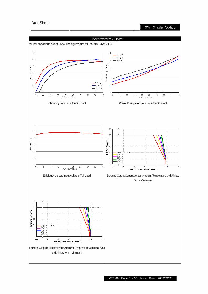
VER:00 Page 15 of 30 Issued Date:2009/03/02
Characteristic Curves (Continued)
All test conditions are at 25°C.The figures are for PXD10-48WS05
Efficiencyversus Output Current Power Dissipation versus Output Current
Efficiencyversus Input Voltage. Full Load DeratingOutputCurrentversusAmbientTemperatureandAirflow
Vin = Vin(nom)
DeratingOutputCurrentVersusAmbientTemperaturewithHeat-Sink
andAirflow,Vin =Vin(nom)

DataSheet10W, Single Output
VER:00 Page 16 of 30 Issued Date:2009/03/02
Characteristic Curves (Continued)
All test conditions are at 25°C.The figures are for PXD10-48WS05
Typical Output Ripple and Noise.
Vin = Vin(nom) ; Full Load
Transient Response to Dynamic Load Change from
100% to 75% to 100% of Full Load ; Vin =Vin(nom)
Typical Input Start-Up and Output Rise Characteristic
Vin = Vin(nom) ; Full Load
Using ON/OFFVoltageStart-Up and Vo Rise Characteristic
Vin = Vin(nom) ; Full Load
ConductionEmission of EN55022 Class A
Vin = Vin(nom) ; Full Load
ConductionEmission of EN55022 Class B
Vin = Vin(nom) ; Full Load

DataSheet10W, Single Output
VER:00 Page 17 of 30 Issued Date:2009/03/02
Characteristic Curves (Continued)
All test conditions are at 25°C.The figures are for PXD10-48WS12
Efficiencyversus Output Current Power Dissipation versus Output Current
Efficiencyversus Input Voltage. Full Load DeratingOutputCurrentversusAmbientTemperatureandAirflow
Vin = Vin(nom)
DeratingOutputCurrentVersusAmbientTemperaturewithHeat-Sink
andAirflow,Vin =Vin(nom)

DataSheet10W, Single Output
VER:00 Page 18 of 30 Issued Date:2009/03/02
Characteristic Curves (Continued)
All test conditions are at 25°C.The figures are for PXD10-48WS12
Typical Output Ripple and Noise.
Vin = Vin(nom) ; Full Load
Transient Response to Dynamic Load Change from
100% to 75% to 100% of Full Load ; Vin =Vin(nom)
Typical Input Start-Up and Output Rise Characteristic
Vin = Vin(nom) ; Full Load
Using ON/OFFVoltageStart-Up and Vo Rise Characteristic
Vin = Vin(nom) ; Full Load
ConductionEmission of EN55022 Class A
Vin = Vin(nom) ; Full Load
ConductionEmission of EN55022 Class B
Vin = Vin(nom) ; Full Load
DataSheet10W, Single Output
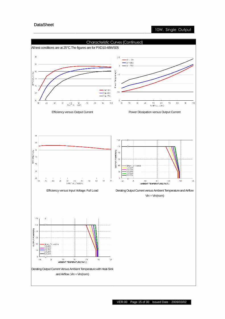
VER:00 Page 19 of 30 Issued Date:2009/03/02
Characteristic Curves (Continued)
All test conditions are at 25°C.The figures are for PXD10-48WS15
Efficiencyversus Output Current Power Dissipation versus Output Current
Efficiencyversus Input Voltage. Full Load DeratingOutputCurrentversusAmbientTemperatureandAirflow
Vin = Vin(nom)
DeratingOutputCurrentVersusAmbientTemperaturewithHeat-Sink
andAirflow,Vin =Vin(nom)

DataSheet10W, Single Output
VER:00 Page 20 of 30 Issued Date:2009/03/02
Characteristic Curves (Continued)
All test conditions are at 25°C.The figures are for PXD10-48WS15
Typical Output Ripple and Noise.
Vin = Vin(nom) ; Full Load
Transient Response to Dynamic Load Change from
100% to 75% to 100% of Full Load ; Vin =Vin(nom)
Typical Input Start-Up and Output Rise Characteristic
Vin = Vin(nom) ; Full Load
Using ON/OFFVoltageStart-Up and Vo Rise Characteristic
Vin = Vin(nom) ; Full Load
ConductionEmission of EN55022 Class A
Vin = Vin(nom) ; Full Load
ConductionEmission of EN55022 Class B
Vin = Vin(nom) ; Full Load

DataSheet10W, Single Output
VER:00 Page 21 of 30 Issued Date:2009/03/02
Testing Configurations
Input reflected-ripple current measurement test:
Component Value Voltage ReferenceL 12μH ---- ----C 100μF 100V Aluminum Electrolytic Capacitor
Peak-to-peak output ripple & noise measurement test
Output voltage and efficiencymeasurement test
Note:All measurements are taken at the module terminals.
%100
inin
oo
IV
IVEfficiency

DataSheet10W, Single Output
VER:00 Page 22 of 30 Issued Date:2009/03/02
EMC considerations
Suggested schematic for EN55022 conducted emission ClassAlimits
Recommended layout with input filter
To meet conducted emissions EN55022 CLASSAthe following components are needed:
PXD10-24WSxx
Component Value Voltage ReferenceC1 1μF 50V 1210 MLCCC2, C3 1000pF 2KV 1808 MLCC
PXD10-48WSxx
Component Value Voltage ReferenceC1 1.5μF 100V 1812 MLCCC2, C3 1000pF 2KV 1808 MLCC

DataSheet10W, Single Output
VER:00 Page 23 of 30 Issued Date:2009/03/02
EMC considerations (Continued)
Suggested schematic for EN55022 conducted emission Class B limits
Recommended layout with input filter
To meet conducted emissions EN55022 CLASS B the following components are needed:
PXD10-24WSxx
Component Value Voltage ReferenceC1 2.2μF 50V 1812 MLCCC3, C4 1000pF 2KV 1808 MLCCL1 325μH ---- Common Choke
PXD10-48WSxx
Component Value Voltage ReferenceC1, C2 2.2μF 100V 1812 MLCCC3, C4 1000pF 2KV 1808 MLCCL1 325μH ---- Common Choke
Common Choke L1 is defined as follows:
■
L-325μH±35% / DCR-35mΩ, max
A height: 8.8 mm, Max
■ Test condition-100kHz / 100mV
■ Recommended through hole-Φ0.8mm
■ All dimensions in millimeters

DataSheet10W, Single Output
VER:00 Page 24 of 30 Issued Date:2009/03/02
Input Source Impedance
The converter should be connected to a low impedance input source. Highly inductive source impedance can
affect the stability of the converter Input external L-C filter is recommended to minimize input reflected ripple current.
The inductor is a simulated source impedance of 12μH and the capacitor is Nippon chemi-con KY series 100μF/100V.
The capacitor must be located as close as possible to the input terminals of the converter for lowest impedance.
Output Over Current Protection
When excessive output currents occur in the system, circuit protection is required on all converters. Normally,
overload current is maintained at approximately 150 percent of rated current for PXF40-xxSxx series.
Hiccup-mode is a method of operation in a converter whose purpose is to protect the power supply from being
damaged during an over-current fault condition. It also enables the converter to restart when the fault is removed.
There are other ways of protecting the converter when it is over-loaded, such as the maximum current limiting or current
foldback methods.
One of the problems resulting from over current is that excessive heat may be generated in power devices;
especially MOSFET and Schottky diodes and the temperature of these devices may exceed their specified limits. A
protection mechanism has to be used to prevent these power devices from being damaged.
The operation of hiccup is as follows. When the current sense circuit sees an over-current event, the controller shuts
off the converter for a given time and then tries to start up the converter again. If the over-load condition has been
removed, the converter will start up and operate normally; otherwise, the controller will see another over-current event
and will shut off the converter again, repeating the previous cycle. Hiccup operation has none of the drawbacks of the
other two protection methods, although its circuit is more complicated because it requires a timing circuit. The excess
heat due to overload lasts for only a short duration in the hiccup cycle, hence the junction temperature of the power
devices is much lower.
Output Over Voltage Protection
The output over-voltage protection consists of an output Zener diode that monitors the voltage on the output
terminals. If the voltage on the output terminals exceeds the over-voltage protection threshold, then the Zener diode
clamps the output voltage.
Short Circuit Protection
Continuous, hiccup and auto-recovery mode.

DataSheet10W, Single Output
VER:00 Page 25 of 30 Issued Date:2009/03/02
Thermal Consideration
The converter operates in a variety of thermal environments; however, sufficient cooling should be provided to help
ensure reliable operation of the unit. Heat is removed by conduction, convection, and radiation to the surrounding
environment. Proper cooling can be verified by measuring the point as shown in the figure below. The temperature at
this location should not exceed 100°C. When Operating, adequate cooling must be provided to maintain the test point
temperature at or below 100°C. Although the maximum point temperature of the power modules is 100°C, lowering
this temperature yields higher reliability.
Measurement shown in inches(mm) TOP VIEW

DataSheet10W, Single Output
VER:00 Page 26 of 30 Issued Date:2009/03/02
Remote ON/OFF Control (Option)
Remote control is an optional feature.
Positive logic:
Turns the module On during logic High on the On/Off pin and turns Off during logic Low.
Negative logic:
Turns the module On during logic Low on the On/Off pin and turns Off during logic High.
The On/Off pin is an open collector/drain logic input signal (Von/off) that referenced to -VIN.
Remote On/Off Implementation
Isolated-Control Remote On/Off
Level Control Using TTLOutput
Level Control Using Line Voltage

DataSheet10W, Single Output
VER:00 Page 27 of 30 Issued Date:2009/03/02
Heat Sink
Use heat-sink (7G-0020A) for lowering temperature and higher reliability of the module.
All dimensions in Inches (mm)
Mechanical Data
PIN CONNECTION
PIN Function
1 + INPUT
2 - INPUT
3 + OUTPUT
5 - OUTPUT
6 CTRL(Option)
1.All dimensions in Inches (mm)
Tolerance:x.xx±0.02 (x.x±0.5)
x.xxx±0.01 (x.xx±0.25)
2. Pin pitch tolerance ±0.01(0.25)
3. Pin dimension tolerance ±0.014(0.35)

DataSheet10W, Single Output
VER:00 Page 28 of 30 Issued Date:2009/03/02
Recommended Pad Layout
1.All dimensions in Inches (mm)
Tolerance:x.xx±0.02 (x.x±0.5)
x.xxx±0.01 (x.xx±0.25)
2. Pin pitch tolerance ±0.01(0.25)
Soldering Considerations
Lead free wave solder profile for PXD10-xxWSxx series.
Zone Reference Parameter
Preheat zone Rise temp. speed : 3°C / sec max.
Preheat temp. : 100~130°C
Actual heating Peak temp. : 250~260°C
Peak time (T1+T2 time) : 4~6 sec
Reference Solder:Sn-Ag-Cu / Sn-Cu
HandWelding: Soldering iron-Power 90W
Welding Time:2-4 sec
Temp.: 380-400 °C

DataSheet10W, Single Output
VER:00 Page 29 of 30 Issued Date:2009/03/02
Packaging Information
All dimensions in millimeters
20 PCS per
Tube
Part Number Structure
Note 1. Maximum value at nominal input voltage and full load of standard type.Note 2. Typical value at nominal input voltage and full load.
Output Current Input CurrentModelNumber
InputRange
OutputVoltage Max. Load Full Load
(1)
Eff(2)
(%)
PXD10-24WS3P3 9 – 36 VDC 3.3VDC 2500mA 465mA 78
PXD10-24WS05 9 – 36 VDC 5VDC 2000mA 548mA 80
PXD10-24WS12 9 – 36 VDC 12VDC 830mA 519mA 84
PXD10-24WS15 9 – 36 VDC 15VDC 670mA 544mA 81
PXD10-48WS3P3 18 – 75 VDC 3.3VDC 2500mA 239mA 76
PXD10-48WS05 18 – 75 VDC 5VDC 2000mA 270mA 81
PXD10-48WS12 18 – 75 VDC 12VDC 830mA 259mA 84
PXD10-48WS15 18 – 75 VDC 15VDC 670mA 262mA 84
Input Voltage Range24 9 ~ 36V48 18 ~ 75V
Max. Output Power10 Watts
Single Output Output Voltage3P3 3.3VDC05 5VDC12 12VDC15 15VDC
Remote ControlNo Suffix: Without Remote ControlSuffix –P: Positive LogicSuffix –N: Negative Logic
4:1 Ultra Wide Input Range
PXD 10 – 48 WS 05 -P

DataSheet10W, Single Output
VER:00 Page 30 of 30 Issued Date:2009/03/02
Safety and Installation Instruction
Fusing Consideration
Caution: This converter is not internally fused.An input line fuse must always be used.
This encapsulated converter can be used in a wide variety of applications, ranging from simple stand-alone operation to
an integrated part of a sophisticated power architecture. For maximum flexibility, internal fusing is not included; however,
to achieve maximum safety and system protection, always use an input line fuse. The safety agencies require a
slow-blow fuse with maximum rating of 5A. Based on the information provided in this data sheet on Inrush energy and
maximum dc input current; the same type of fuse with lower rating can be used. Refer to the fuse manufacturer’s data
for further information.
MTBF and Reliability
The MTBF of PXD10-xxWSxx series of DC/DC converters has been calculated using
Bellcore TR-NWT-000332 Case I: 50% stress, Operating Temperature at 40°C (Ground fixed and controlled
environment ). The resulting figure for MTBF is 1.976×10⁶hours.
MIL-HDBK 217F NOTICE2 FULL LOAD, Operating Temperature at 25℃°C. The resulting figure for MTBF is
1.416 × 10⁶hours.