Embed Size (px)
Citation preview
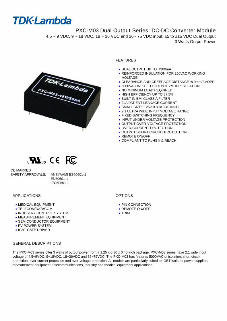
PXC-M03 Dual Output Series: DC-DC Converter Module4.5 ~ 9 VDC, 9 ~ 18 VDC, 18 ~ 36 VDC and 36~ 75 VDC input; ±5 to ±15 VDC Dual Output
3 Watts Output Power
FEATURES
DUAL OUTPUT UP TO ±300mA REINFORCED INSULATION FOR 250VAC WORKING
VOLTAGE CLEARANCE AND CREEPAGE DISTANCE :8.0mm/2MOPP 5000VAC INPUT TO OUTPUT 2MOPP ISOLATION NO MINIMUM LOAD REQUIRED HIGH EFFICIENCY UP TO 87.5% BUILT-IN EMI CLASS A FILTER 2μA PATIENT LEAKAGE CURRENT SMALL SIZE: 1.250.800.40 INCH 2:1 ULTRA WIDE INPUT VOLTAGE RANGE FIXED SWITCHING FREQUENCY INPUT UNDER-VOLTAGE PROTECTION OUTPUT OVER-VOLTAGE PROTECTION OVER-CURRENT PROTECTION OUTPUT SHORT CIRCUIT PROTECTION REMOTE ON/OFF COMPLIANT TO RoHS II & REACH
CE MARKEDSAFETY APPROVALS: ANSI/AAMI ES60601-1
EN60601-1IEC60601-1
APPLICATIONS OPTIONS
MEDICAL EQUIPMENT TELECOM/DATACOM INDUSTRY CONTROL SYSTEM MEASUREMENT EQUIPMENT SEMICONDUCTOR EQUIPMENT PV POWER SYSTEM IGBT GATE DRIVER
PIN CONNECTION REMOTE ON/OFF TRIM
GENERAL DESCRIPTIONS
The PXC-M03 series offer 3 watts of output power from a 1.25 x 0.80 x 0.40 inch package. PXC-M03 series have 2:1 wide inputvoltage of 4.5~9VDC, 9~18VDC, 18~36VDC and 36~75VDC. The PXC-M03 has features 5000VAC of isolation, short circuitprotection, over-current protection and over-voltage protection. All models are particularly suited to IGBT isolated power supplies,measurement equipment, telecommunications, industry and medical equipment applications.
PXC-M03-DUAL
2 Application Note www.us.tdk-lambda.com/lp VER: 03 2015/05/15
Contents
Output Specifications 3Input Specifications 4General Specifications 5Environmental Specifications 5EMC Characteristics 5Characteristic Curves
PXC-M03-05D05 6PXC-M03-05D12 8PXC-M03-05D15 10PXC-M03-12D05 12PXC-M03-12D12 14PXC-M03-12D15 16PXC-M03-24D05 18PXC-M03-24D12 20PXC-M03-24D15 22PXC-M03-48D05 24PXC-M03-48D12 26PXC-M03-48D15 28
Output Voltage Adjustment 30Input Source Impedance 31Output Over Current Protection 32Output Short Circuitry Protection 32Output Over Voltage Protection 32Thermal Considerations 32Remote On/off Control 33EMS Considerations 34Mechanical Data 35Recommended Pad Layout 36Soldering Considerations 36Packaging Information 37Part Number Structure 37Safety and Installation Instruction 37MTBF and Reliability 37
PXC-M03-DUAL
3 Application Note www.us.tdk-lambda.com/lp VER: 03 2015/05/15
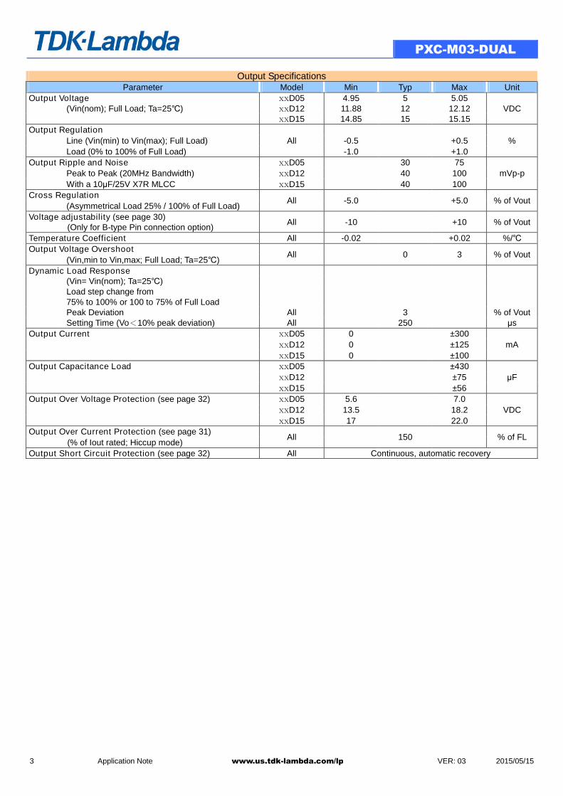
Output SpecificationsParameter Model Min Typ Max Unit
Output Voltage xxD05 4.95 5 5.05VDC(Vin(nom); Full Load; Ta=25℃) xxD12 11.88 12 12.12
xxD15 14.85 15 15.15
Output Regulation
All %Line (Vin(min) to Vin(max); Full Load) -0.5 +0.5
Load (0% to 100% of Full Load) -1.0 +1.0
Output Ripple and Noise xxD05 30 75
mVp-pPeak to Peak (20MHz Bandwidth) xxD12 40 100
With a 10μF/25V X7R MLCC xxD15 40 100
Cross RegulationAll -5.0 +5.0 % of Vout
(Asymmetrical Load 25% / 100% of Full Load)
Voltage adjustability (see page 30)(Only for B-type Pin connection option)
All -10 +10 % of Vout
Temperature Coefficient All -0.02 +0.02 %/℃
Output Voltage OvershootAll 0 3 % of Vout
(Vin,min to Vin,max; Full Load; Ta=25℃)
Dynamic Load Response(Vin= Vin(nom); Ta=25℃)Load step change from75% to 100% or 100 to 75% of Full LoadPeak Deviation All 3 % of VoutSetting Time (Vo<10% peak deviation) All 250 μs
Output Current xxD05 0 ±300
mAxxD12 0 ±125
xxD15 0 ±100
Output Capacitance Load xxD05 ±430
μFxxD12 ±75
xxD15 ±56
Output Over Voltage Protection (see page 32) xxD05 5.6 7.0
VDCxxD12 13.5 18.2
xxD15 17 22.0
Output Over Current Protection (see page 31)All 150 % of FL
(% of Iout rated; Hiccup mode)
Output Short Circuit Protection (see page 32) All Continuous, automatic recovery
PXC-M03-DUAL
4 Application Note www.us.tdk-lambda.com/lp VER: 03 2015/05/15
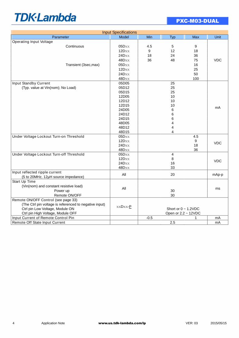
Input SpecificationsParameter Model Min Typ Max Unit
Operating Input Voltage
VDC
Continuous 05Dxx 4.5 5 9
12Dxx 9 12 18
24Dxx 18 24 36
48Dxx 36 48 75
Transient (3sec,max) 05Dxx 16
12Dxx 25
24Dxx 50
48Dxx 100
Input Standby Current 05D05 25
mA
(Typ. value at Vin(nom); No Load) 05D12 2505D15 2512D05 1012D12 1012D15 1024D05 624D12 624D15 648D05 448D12 448D15 4
Under Voltage Lockout Turn-on Threshold 05Dxx 4.5
VDC12Dxx 924Dxx 1848Dxx 36
Under Voltage Lockout Turn-off Threshold 05Dxx 4
VDC12Dxx 824Dxx 1648Dxx 33
Input reflected ripple currentAll 20 mAp-p
(5 to 20MHz, 12μH source impedance)
Start Up Time
All ms(Vin(nom) and constant resistive load)
Power up 30
Remote ON/OFF 30
Remote ON/OFF Control (see page 33)
xxDxx-P(The Ctrl pin voltage is referenced to negative input)Ctrl pin Low Voltage, Module ON Short or 0 ~ 1.2VDCCtrl pin High Voltage, Module OFF Open or 2.2 ~ 12VDC
Input Current of Remote Control Pin -0.5 1 mA
Remote Off State Input Current 2.5 mA
PXC-M03-DUAL
5 Application Note www.us.tdk-lambda.com/lp VER: 03 2015/05/15
General SpecificationsParameter Model Min Typ Max Unit
Efficiency 05D05 83
%
(Vin(nom); Full Load; Ta=25℃) 05D12 8605D15 8612D05 83.512D12 87.512D15 86.524D05 8324D12 8724D15 8648D05 8348D12 8648D15 86
Isolation voltage (1 minute)All VAC
Input to Output 5000
Isolation capacitance All 12 17 pF
Leakage current (240VAC,60Hz) All 2 μA
Switching Frequency All 135 150 165 kHz
Clearance/Creepage All 8 mm
Weight All 14.0 g
MTBF(see page 37)All hours
MIL-HDBK-217F Ta=25ºC, Full load 6.444 x 10⁶
Safety ApprovalsAll
ANSI/AAMI ES60601-1IEC60601-1, EN60601-1
Case Material Non-conductive black plastic
Base Material All Non-conductive black plastic
Potting Material All Silicone (UL94 V-0)
Environmental SpecificationsParameter Model Min Typ Max Unit
Operating Ambient Temperature
All ℃Without Derating -40 94
With Derating 94 105
Storage Temperature All -55 125 ℃
Thermal Impedance (20LFM) All 18 ℃/W
Relative humidity All 5 95 % RH
Thermal Shock All MIL-STD-810F
Vibration All MIL-STD-810F
EMC CharacteristicsCharacteristic Standard Condition Level
EMI EN55011
Module stand-alone Class AEN55022
FCC Part 18
EN55011
With external input filter Class BEN55022
FCC Part 18
ESD EN61000-4-2Air ±8kV
Perf. Criteria AContact ±6kV
Radiated Immunity EN61000-4-3 10V/m Perf. Criteria A
Fast Transient(see page 34) EN61000-4-4 ±2kV Perf. Criteria A
Surge(see page 34) EN61000-4-5 ±2kV Perf. Criteria A
Conducted Immunity EN61000-4-6 10V r.m.s Perf. Criteria A
PXC-M03-DUAL
6 Application Note www.us.tdk-lambda.com/lp VER: 03 2015/05/15
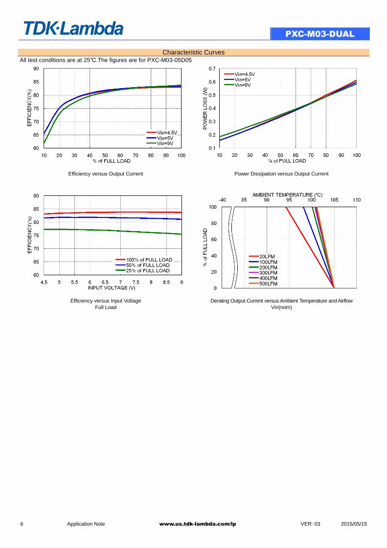
Characteristic CurvesAll test conditions are at 25℃.The figures are for PXC-M03-05D05
Efficiency versus Output Current Power Dissipation versus Output Current
Efficiency versus Input Voltage Derating Output Current versus Ambient Temperature and AirflowFull Load Vin(nom)
PXC-M03-DUAL
7 Application Note www.us.tdk-lambda.com/lp VER: 03 2015/05/15
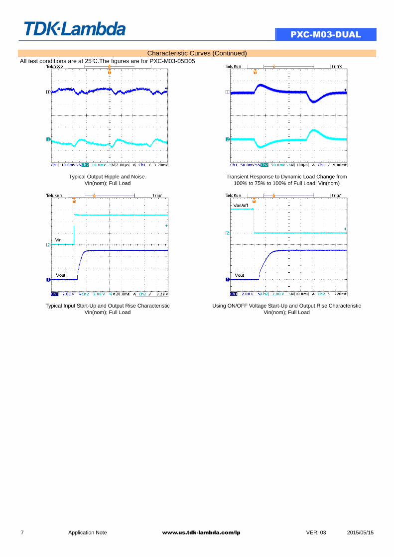
Characteristic Curves (Continued)All test conditions are at 25℃.The figures are for PXC-M03-05D05
Typical Output Ripple and Noise. Transient Response to Dynamic Load Change fromVin(nom); Full Load 100% to 75% to 100% of Full Load; Vin(nom)
Typical Input Start-Up and Output Rise Characteristic Using ON/OFF Voltage Start-Up and Output Rise CharacteristicVin(nom); Full Load Vin(nom); Full Load
PXC-M03-DUAL
8 Application Note www.us.tdk-lambda.com/lp VER: 03 2015/05/15
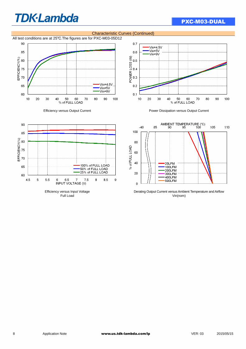
Characteristic Curves (Continued)All test conditions are at 25℃.The figures are for PXC-M03-05D12
Efficiency versus Output Current Power Dissipation versus Output Current
Efficiency versus Input Voltage Derating Output Current versus Ambient Temperature and AirflowFull Load Vin(nom)
PXC-M03-DUAL
9 Application Note www.us.tdk-lambda.com/lp VER: 03 2015/05/15
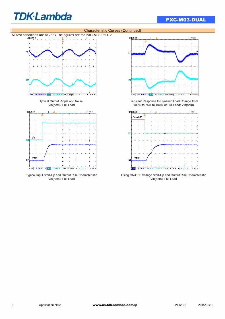
Characteristic Curves (Continued)All test conditions are at 25℃.The figures are for PXC-M03-05D12
Typical Output Ripple and Noise. Transient Response to Dynamic Load Change fromVin(nom); Full Load 100% to 75% to 100% of Full Load; Vin(nom)
Typical Input Start-Up and Output Rise Characteristic Using ON/OFF Voltage Start-Up and Output Rise CharacteristicVin(nom); Full Load Vin(nom); Full Load
PXC-M03-DUAL
10 Application Note www.us.tdk-lambda.com/lp VER: 03 2015/05/15
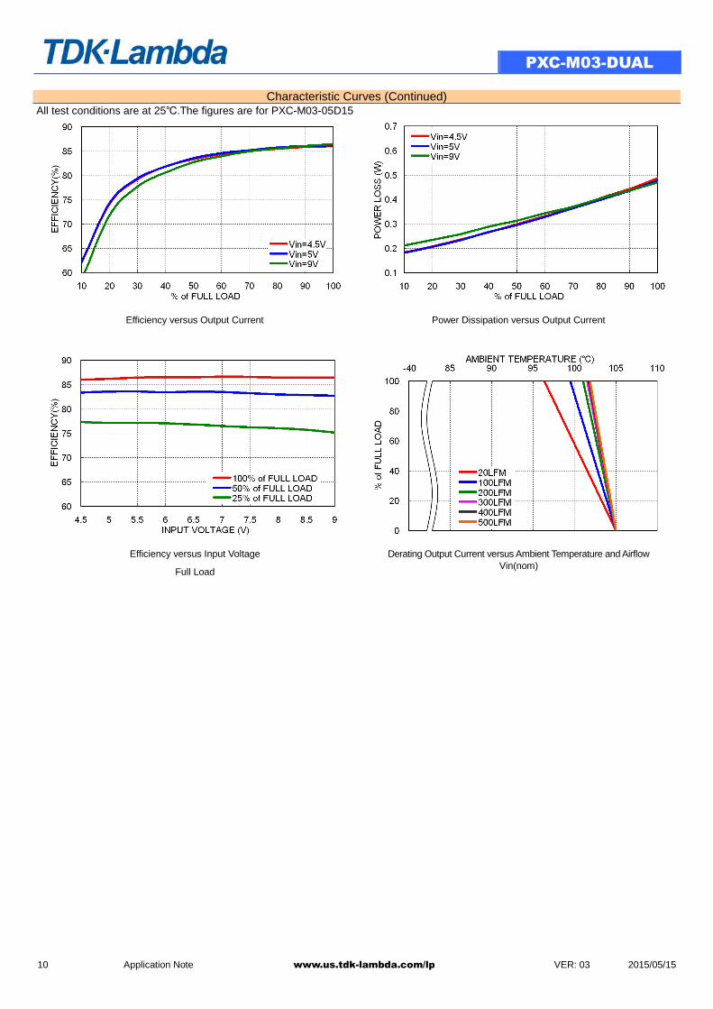
Characteristic Curves (Continued)All test conditions are at 25℃.The figures are for PXC-M03-05D15
Efficiency versus Output Current Power Dissipation versus Output Current
Efficiency versus Input Voltage Derating Output Current versus Ambient Temperature and Airflow
Full LoadVin(nom)
PXC-M03-DUAL
11 Application Note www.us.tdk-lambda.com/lp VER: 03 2015/05/15
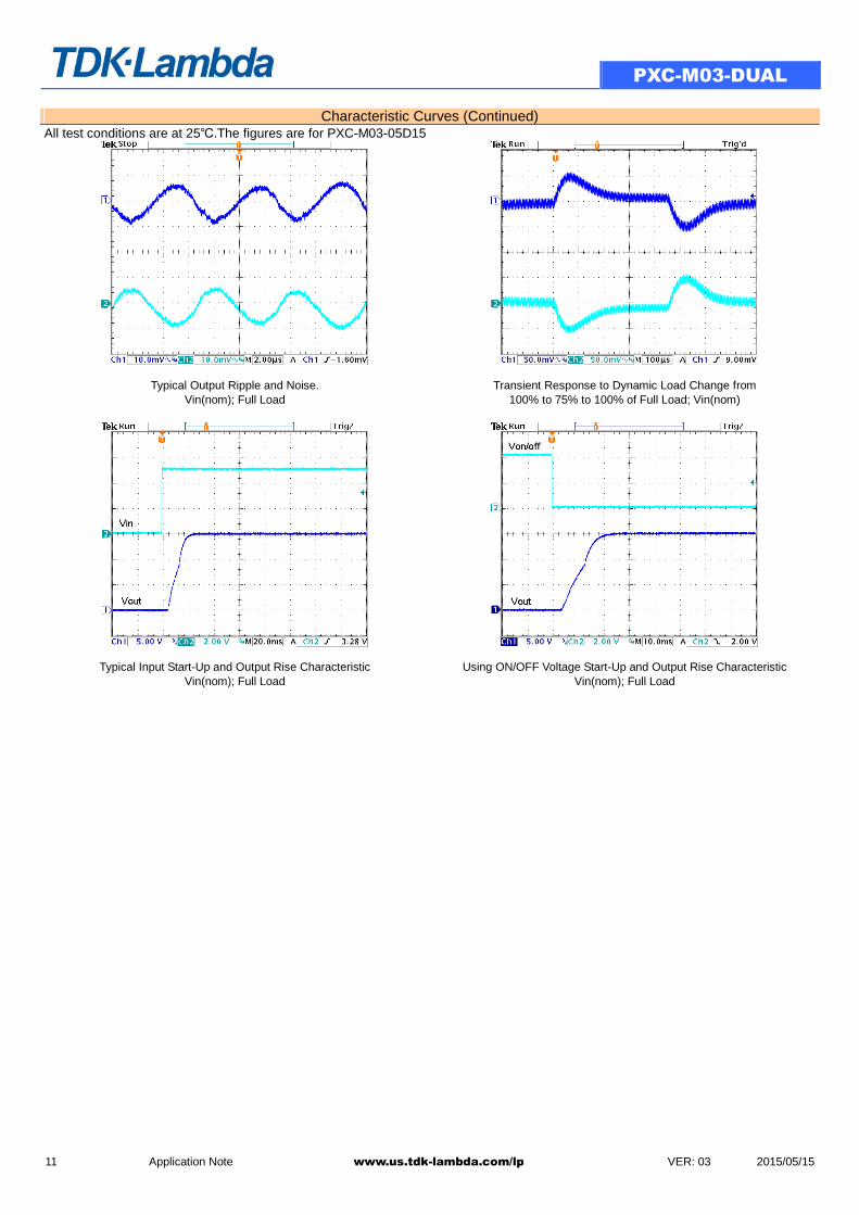
Characteristic Curves (Continued)All test conditions are at 25℃.The figures are for PXC-M03-05D15
Typical Output Ripple and Noise. Transient Response to Dynamic Load Change fromVin(nom); Full Load 100% to 75% to 100% of Full Load; Vin(nom)
Typical Input Start-Up and Output Rise Characteristic Using ON/OFF Voltage Start-Up and Output Rise CharacteristicVin(nom); Full Load Vin(nom); Full Load
PXC-M03-DUAL
12 Application Note www.us.tdk-lambda.com/lp VER: 03 2015/05/15
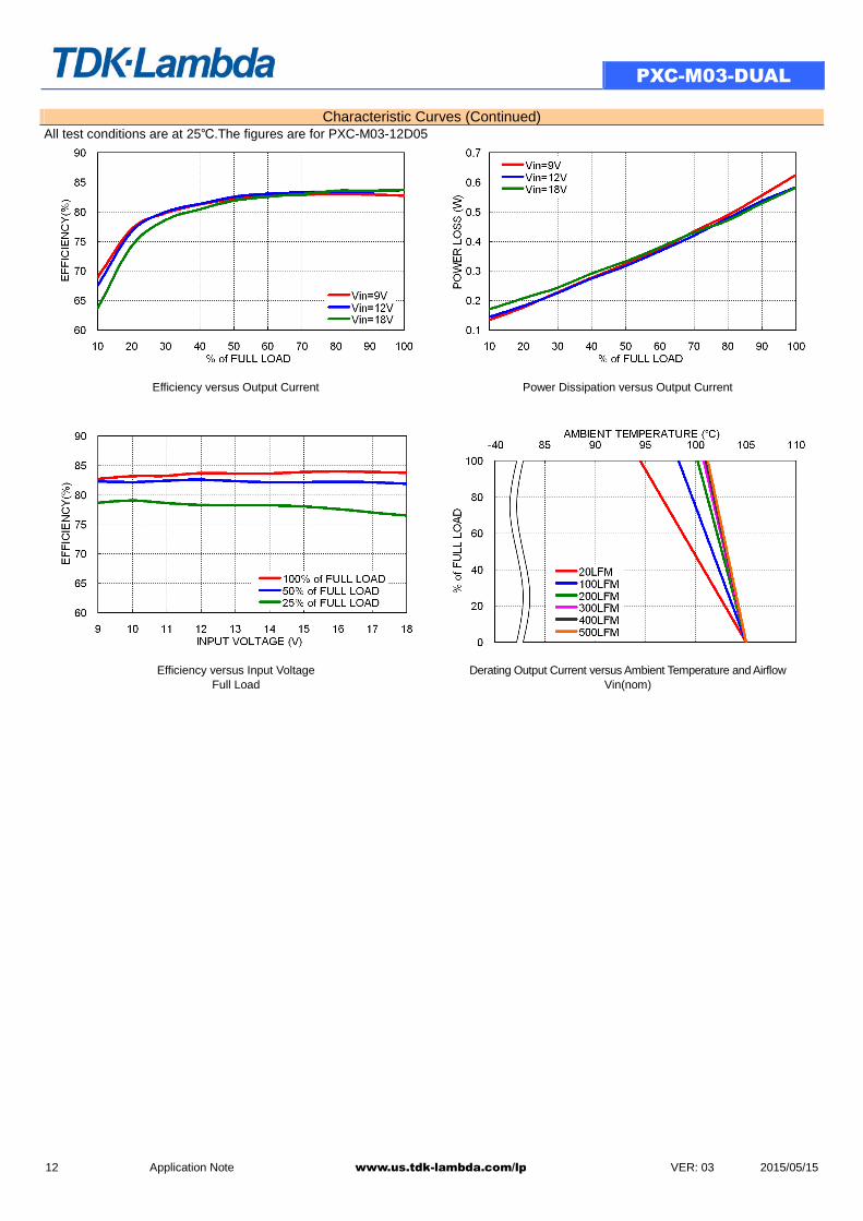
Characteristic Curves (Continued)All test conditions are at 25℃.The figures are for PXC-M03-12D05
Efficiency versus Output Current Power Dissipation versus Output Current
Efficiency versus Input Voltage Derating Output Current versus Ambient Temperature and AirflowFull Load Vin(nom)
PXC-M03-DUAL
13 Application Note www.us.tdk-lambda.com/lp VER: 03 2015/05/15
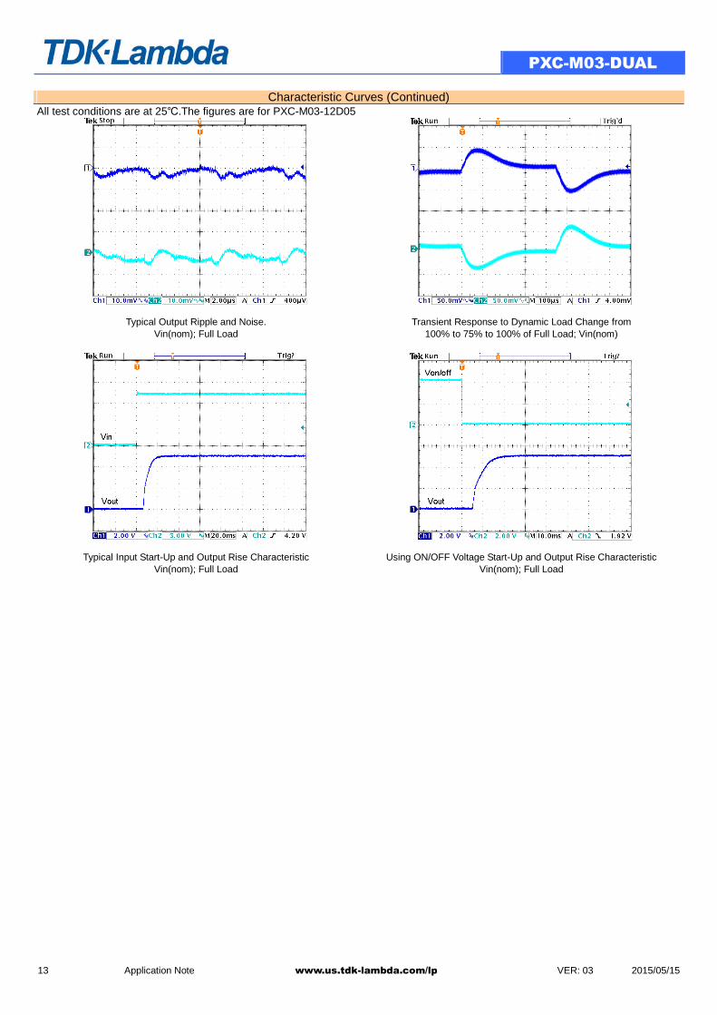
Characteristic Curves (Continued)All test conditions are at 25℃.The figures are for PXC-M03-12D05
Typical Output Ripple and Noise. Transient Response to Dynamic Load Change fromVin(nom); Full Load 100% to 75% to 100% of Full Load; Vin(nom)
Typical Input Start-Up and Output Rise Characteristic Using ON/OFF Voltage Start-Up and Output Rise CharacteristicVin(nom); Full Load Vin(nom); Full Load
PXC-M03-DUAL
14 Application Note www.us.tdk-lambda.com/lp VER: 03 2015/05/15
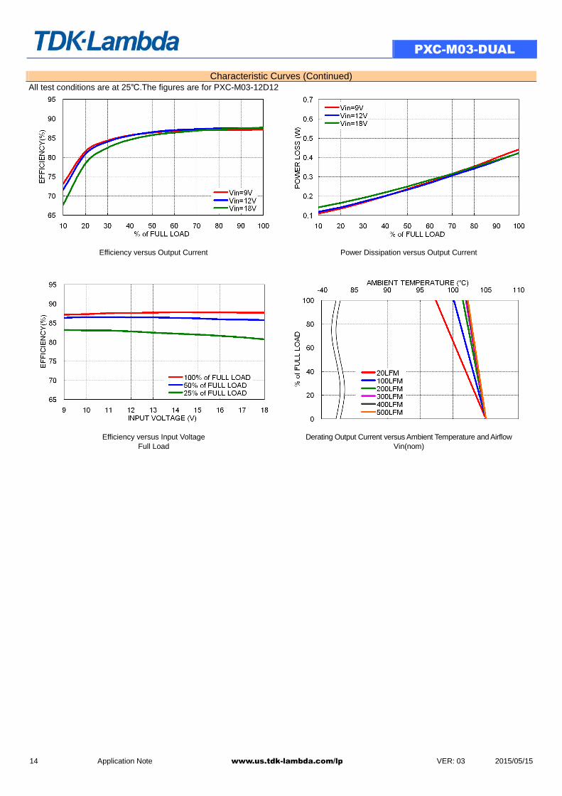
Characteristic Curves (Continued)All test conditions are at 25℃.The figures are for PXC-M03-12D12
Efficiency versus Output Current Power Dissipation versus Output Current
Efficiency versus Input Voltage Derating Output Current versus Ambient Temperature and AirflowFull Load Vin(nom)
PXC-M03-DUAL
15 Application Note www.us.tdk-lambda.com/lp VER: 03 2015/05/15
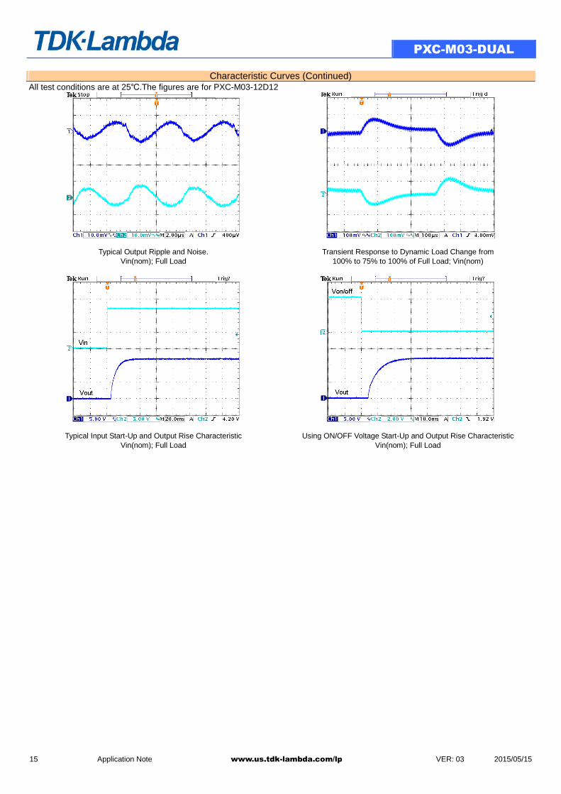
Characteristic Curves (Continued)All test conditions are at 25℃.The figures are for PXC-M03-12D12
Typical Output Ripple and Noise. Transient Response to Dynamic Load Change fromVin(nom); Full Load 100% to 75% to 100% of Full Load; Vin(nom)
Typical Input Start-Up and Output Rise Characteristic Using ON/OFF Voltage Start-Up and Output Rise CharacteristicVin(nom); Full Load Vin(nom); Full Load
PXC-M03-DUAL
16 Application Note www.us.tdk-lambda.com/lp VER: 03 2015/05/15
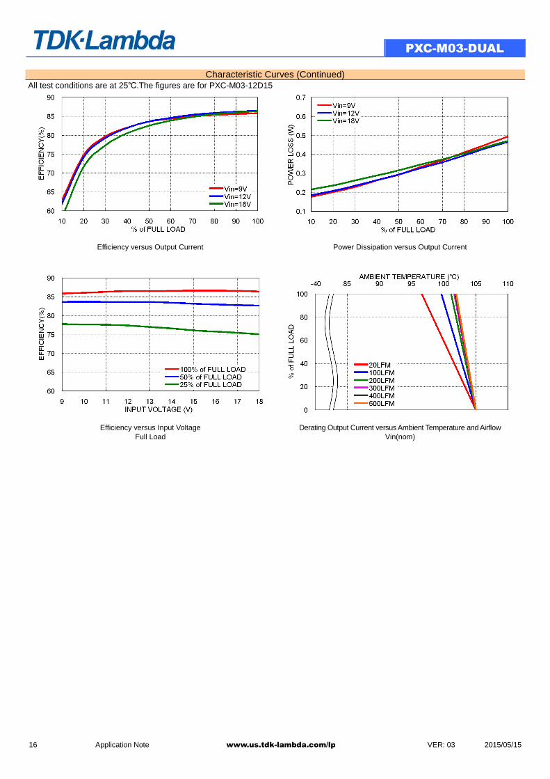
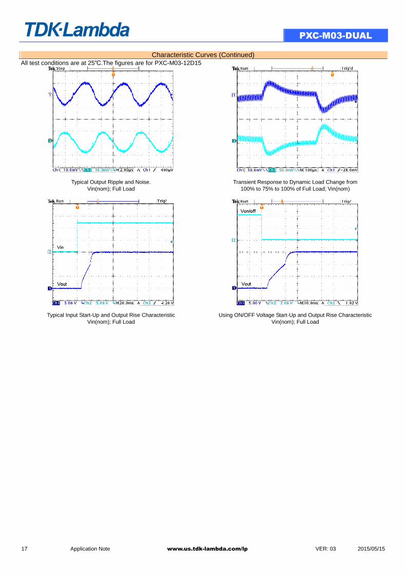
Characteristic Curves (Continued)All test conditions are at 25℃.The figures are for PXC-M03-12D15
Efficiency versus Output Current Power Dissipation versus Output Current
Efficiency versus Input Voltage Derating Output Current versus Ambient Temperature and AirflowFull Load Vin(nom)
PXC-M03-DUAL
17 Application Note www.us.tdk-lambda.com/lp VER: 03 2015/05/15
Characteristic Curves (Continued)All test conditions are at 25℃.The figures are for PXC-M03-12D15
Typical Output Ripple and Noise. Transient Response to Dynamic Load Change fromVin(nom); Full Load 100% to 75% to 100% of Full Load; Vin(nom)
Typical Input Start-Up and Output Rise Characteristic Using ON/OFF Voltage Start-Up and Output Rise CharacteristicVin(nom); Full Load Vin(nom); Full Load
PXC-M03-DUAL
18 Application Note www.us.tdk-lambda.com/lp VER: 03 2015/05/15
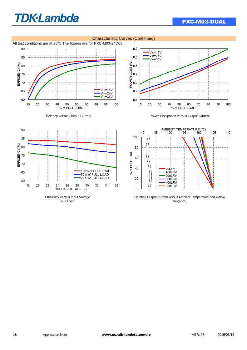
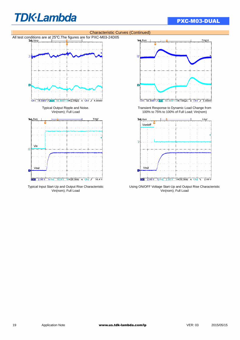
Characteristic Curves (Continued)All test conditions are at 25℃.The figures are for PXC-M03-24D05
Efficiency versus Output Current Power Dissipation versus Output Current
Efficiency versus Input Voltage Derating Output Current versus Ambient Temperature and AirflowFull Load Vin(nom)
PXC-M03-DUAL
19 Application Note www.us.tdk-lambda.com/lp VER: 03 2015/05/15
Characteristic Curves (Continued)All test conditions are at 25℃.The figures are for PXC-M03-24D05
Typical Output Ripple and Noise. Transient Response to Dynamic Load Change fromVin(nom); Full Load 100% to 75% to 100% of Full Load; Vin(nom)
Typical Input Start-Up and Output Rise Characteristic Using ON/OFF Voltage Start-Up and Output Rise CharacteristicVin(nom); Full Load Vin(nom); Full Load
PXC-M03-DUAL
20 Application Note www.us.tdk-lambda.com/lp VER: 03 2015/05/15
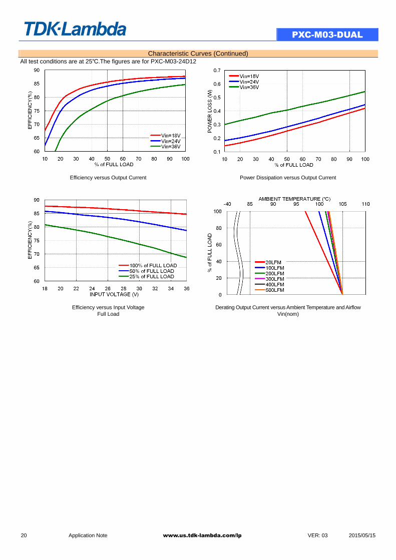
Characteristic Curves (Continued)All test conditions are at 25℃.The figures are for PXC-M03-24D12
Efficiency versus Output Current Power Dissipation versus Output Current
Efficiency versus Input Voltage Derating Output Current versus Ambient Temperature and AirflowFull Load Vin(nom)
PXC-M03-DUAL
21 Application Note www.us.tdk-lambda.com/lp VER: 03 2015/05/15
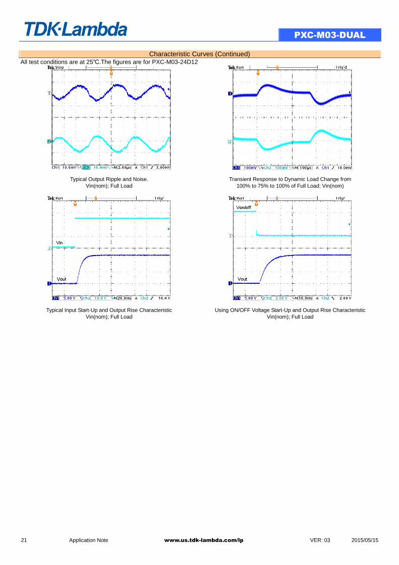
Characteristic Curves (Continued)All test conditions are at 25℃.The figures are for PXC-M03-24D12
Typical Output Ripple and Noise. Transient Response to Dynamic Load Change fromVin(nom); Full Load 100% to 75% to 100% of Full Load; Vin(nom)
Typical Input Start-Up and Output Rise Characteristic Using ON/OFF Voltage Start-Up and Output Rise CharacteristicVin(nom); Full Load Vin(nom); Full Load
PXC-M03-DUAL
22 Application Note www.us.tdk-lambda.com/lp VER: 03 2015/05/15
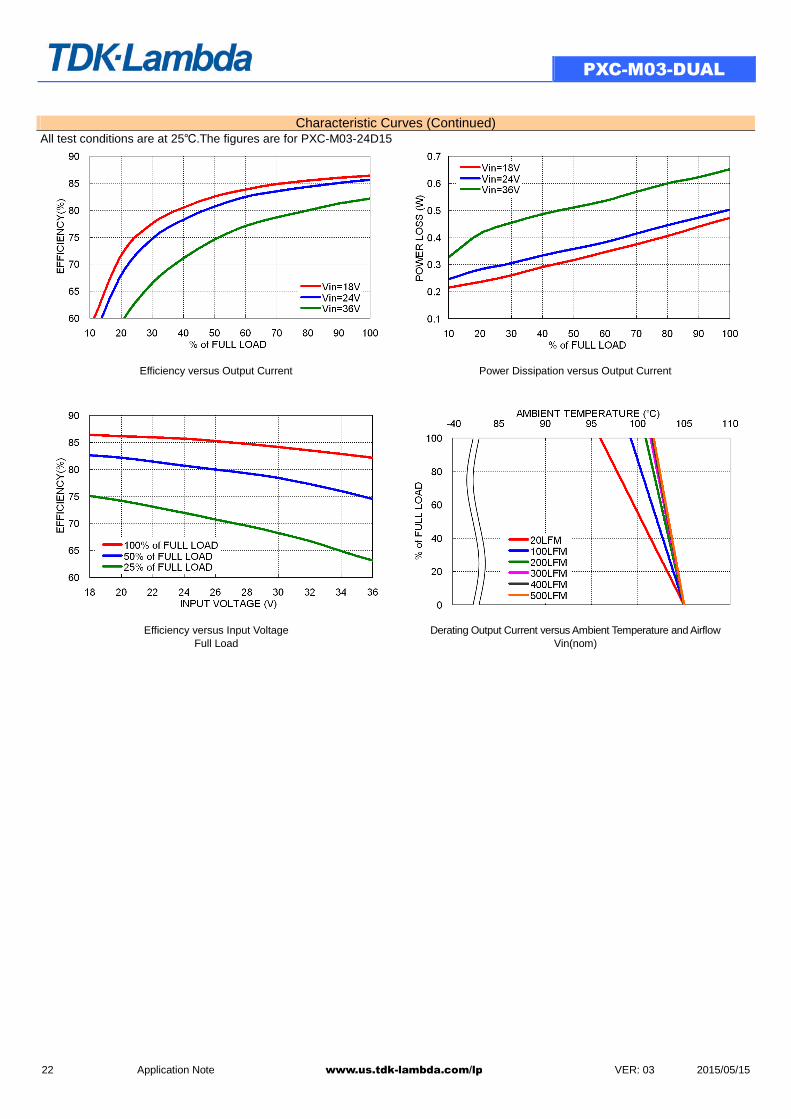
Characteristic Curves (Continued)All test conditions are at 25℃.The figures are for PXC-M03-24D15
Efficiency versus Output Current Power Dissipation versus Output Current
Efficiency versus Input Voltage Derating Output Current versus Ambient Temperature and AirflowFull Load Vin(nom)
PXC-M03-DUAL
23 Application Note www.us.tdk-lambda.com/lp VER: 03 2015/05/15
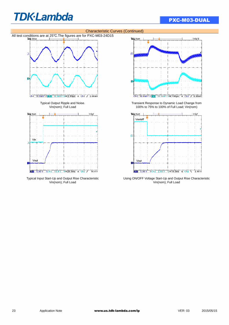
Characteristic Curves (Continued)All test conditions are at 25℃.The figures are for PXC-M03-24D15
Typical Output Ripple and Noise. Transient Response to Dynamic Load Change fromVin(nom); Full Load 100% to 75% to 100% of Full Load; Vin(nom)
Typical Input Start-Up and Output Rise Characteristic Using ON/OFF Voltage Start-Up and Output Rise CharacteristicVin(nom); Full Load Vin(nom); Full Load
PXC-M03-DUAL
24 Application Note www.us.tdk-lambda.com/lp VER: 03 2015/05/15
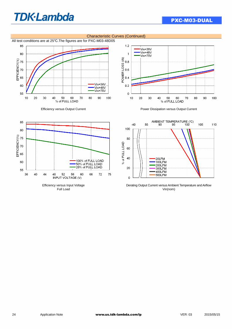
Characteristic Curves (Continued)All test conditions are at 25℃.The figures are for PXC-M03-48D05
Efficiency versus Output Current Power Dissipation versus Output Current
Efficiency versus Input Voltage Derating Output Current versus Ambient Temperature and AirflowFull Load Vin(nom)
PXC-M03-DUAL
25 Application Note www.us.tdk-lambda.com/lp VER: 03 2015/05/15
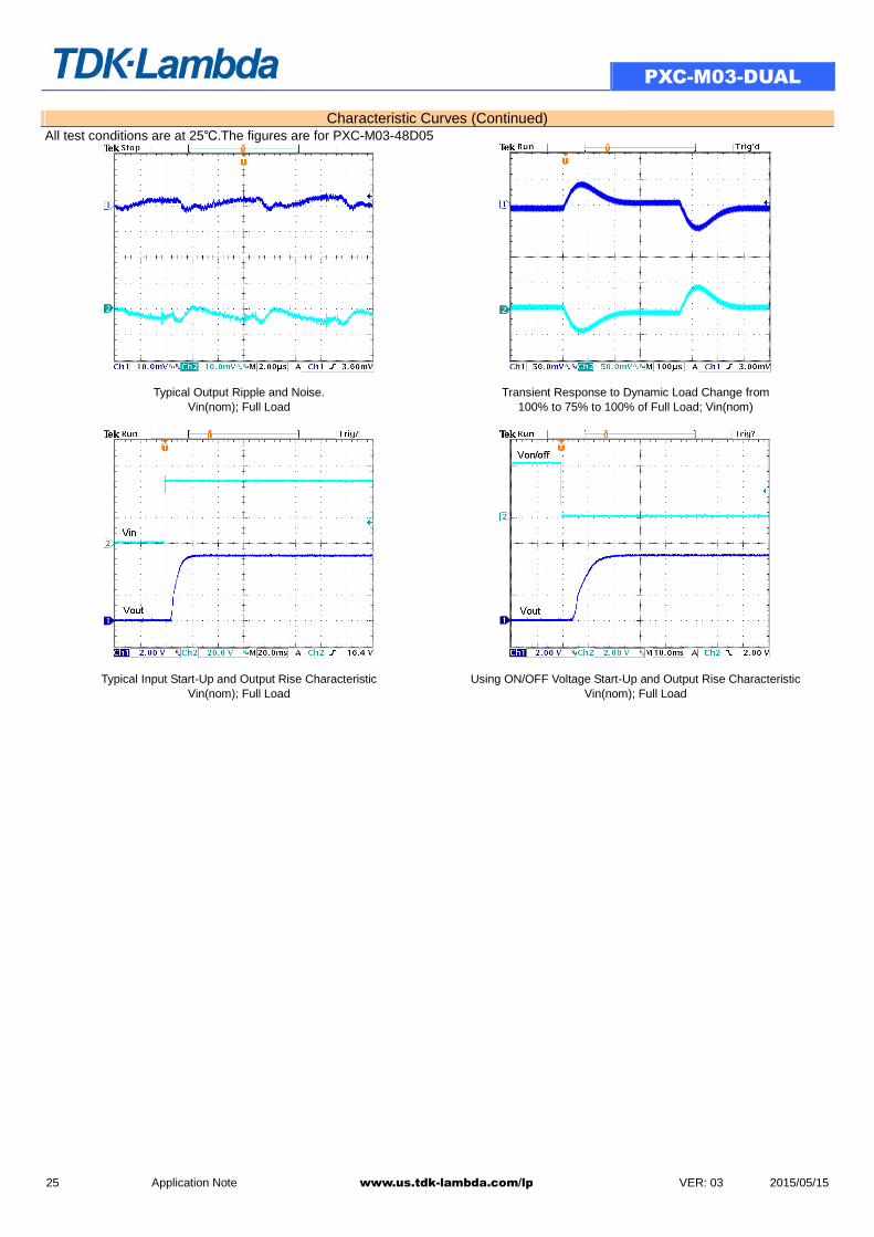
Characteristic Curves (Continued)All test conditions are at 25℃.The figures are for PXC-M03-48D05
Typical Output Ripple and Noise. Transient Response to Dynamic Load Change fromVin(nom); Full Load 100% to 75% to 100% of Full Load; Vin(nom)
Typical Input Start-Up and Output Rise Characteristic Using ON/OFF Voltage Start-Up and Output Rise CharacteristicVin(nom); Full Load Vin(nom); Full Load
PXC-M03-DUAL
26 Application Note www.us.tdk-lambda.com/lp VER: 03 2015/05/15
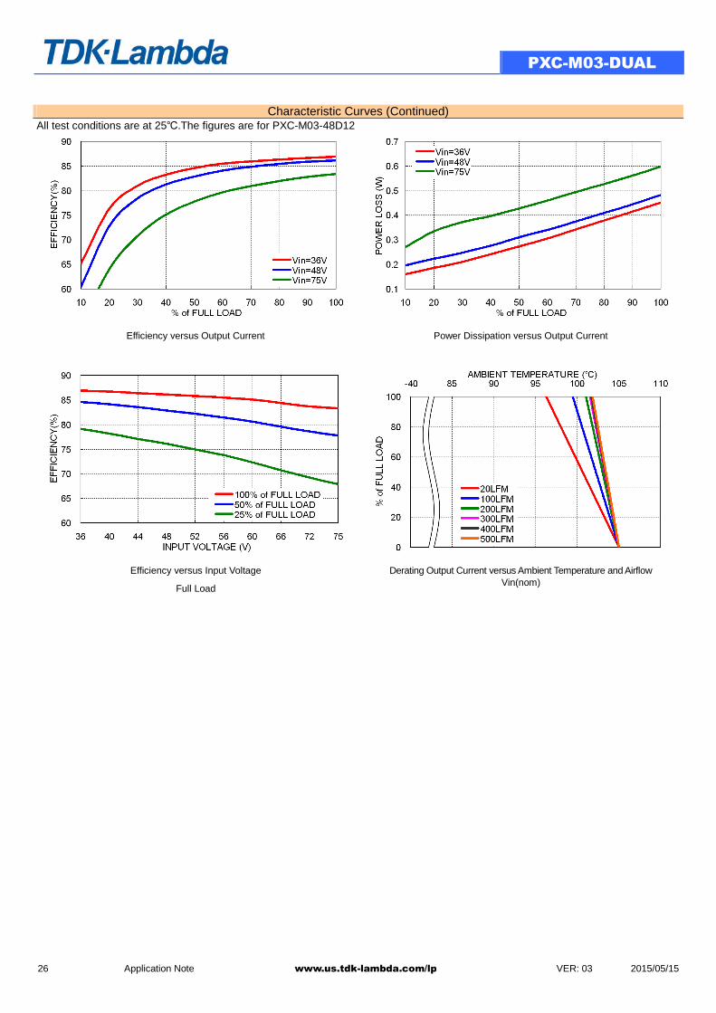
Characteristic Curves (Continued)All test conditions are at 25℃.The figures are for PXC-M03-48D12
Efficiency versus Output Current Power Dissipation versus Output Current
Efficiency versus Input Voltage Derating Output Current versus Ambient Temperature and Airflow
Full LoadVin(nom)
PXC-M03-DUAL
27 Application Note www.us.tdk-lambda.com/lp VER: 03 2015/05/15
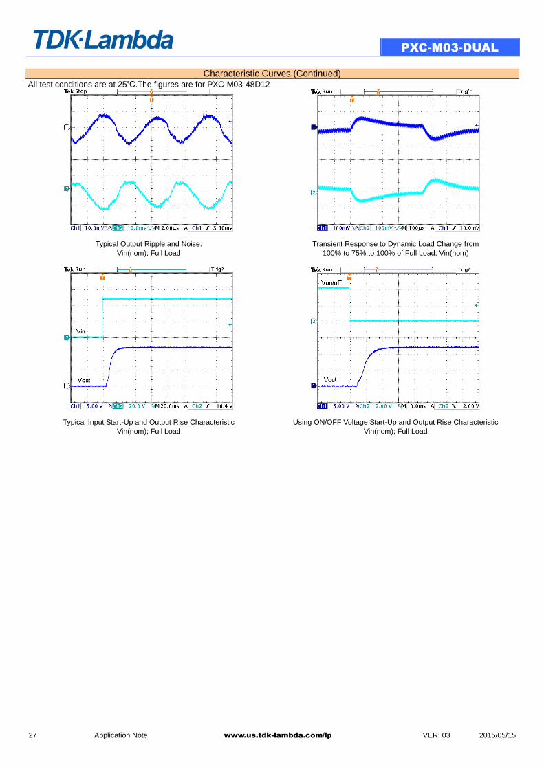
Characteristic Curves (Continued)All test conditions are at 25℃.The figures are for PXC-M03-48D12
Typical Output Ripple and Noise. Transient Response to Dynamic Load Change fromVin(nom); Full Load 100% to 75% to 100% of Full Load; Vin(nom)
Typical Input Start-Up and Output Rise Characteristic Using ON/OFF Voltage Start-Up and Output Rise CharacteristicVin(nom); Full Load Vin(nom); Full Load
PXC-M03-DUAL
28 Application Note www.us.tdk-lambda.com/lp VER: 03 2015/05/15
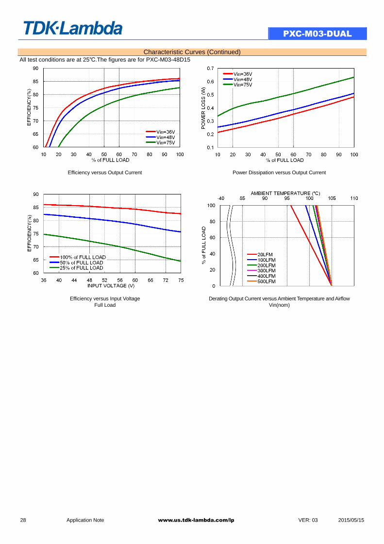
Characteristic Curves (Continued)All test conditions are at 25℃.The figures are for PXC-M03-48D15
Efficiency versus Output Current Power Dissipation versus Output Current
Efficiency versus Input Voltage Derating Output Current versus Ambient Temperature and AirflowFull Load Vin(nom)
PXC-M03-DUAL
29 Application Note www.us.tdk-lambda.com/lp VER: 03 2015/05/15
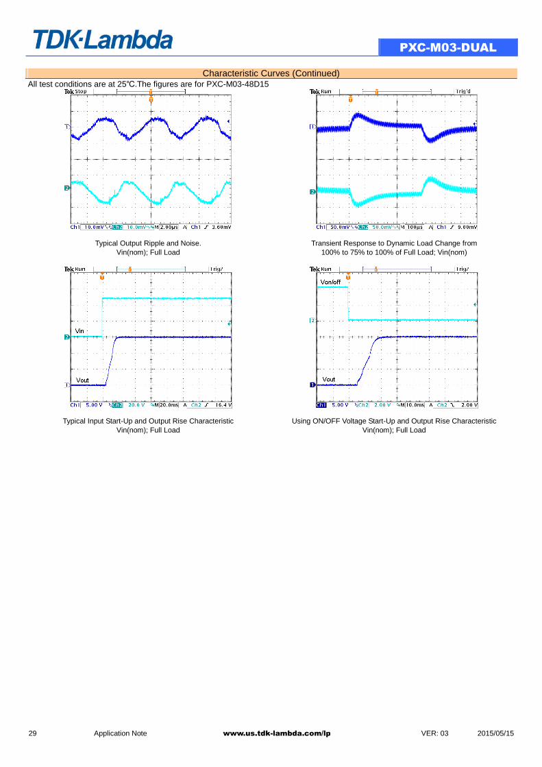
Characteristic Curves (Continued)All test conditions are at 25℃.The figures are for PXC-M03-48D15
Typical Output Ripple and Noise. Transient Response to Dynamic Load Change fromVin(nom); Full Load 100% to 75% to 100% of Full Load; Vin(nom)
Typical Input Start-Up and Output Rise Characteristic Using ON/OFF Voltage Start-Up and Output Rise CharacteristicVin(nom); Full Load Vin(nom); Full Load
PXC-M03-DUAL
30 Application Note www.us.tdk-lambda.com/lp VER: 03 2015/05/15
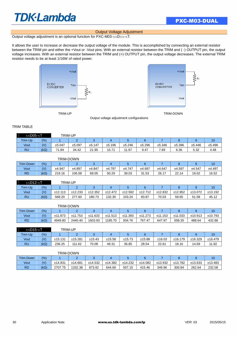
Output Voltage AdjustmentOutput voltage adjustment is an optional function for PXC-M03-xxDxx-xT.
It allows the user to increase or decrease the output voltage of the module. This is accomplished by connecting an external resistorbetween the TRIM pin and either the +Vout or -Vout pins. With an external resistor between the TRIM and ( -) OUTPUT pin, the outputvoltage increases. With an external resistor between the TRIM and (+) OUTPUT pin, the output voltage decreases. The external TRIMresistor needs to be at least 1/16W of rated power.
TRIM-UP TRIM-DOWN
Output voltage adjustment configurations
TRIM TABLE
xxD05-xT TRIM-UP
Trim-Up (%) 1 2 3 4 5 6 7 8 9 10
Vout (V) ±5.047 ±5.097 ±5.147 ±5.196 ±5.246 ±5.296 ±5.346 ±5.396 ±5.446 ±5.496
RU (kΩ) 71.84 34.42 21.95 15.71 11.97 9.47 7.69 6.36 5.32 4.48
TRIM-DOWN
Trim-Down (%) 1 2 3 4 5 6 7 8 9 10
Vout (V) ±4.947 ±4.897 ±4.847 ±4.797 ±4.747 ±4.697 ±4.647 ±4.597 ±4.547 ±4.497
RD (kΩ) 219.16 106.58 69.05 50.29 39.03 31.53 26.17 22.14 19.02 16.52
xxD12-xT TRIM-UP
Trim-Up (%) 1 2 3 4 5 6 7 8 9 10
Vout (V) ±12.113 ±12.233 ±12.352 ±12.472 ±12.592 ±12.712 ±12.832 ±12.952 ±13.072 ±13.192
RU (kΩ) 568.20 277.60 180.73 132.30 103.24 83.87 70.03 59.65 51.58 45.12
TRIM-DOWN
Trim-Down (%) 1 2 3 4 5 6 7 8 9 10
Vout (V) ±11.873 ±11.753 ±11.633 ±11.513 ±11.393 ±11.273 ±11.153 ±11.033 ±10.913 ±10.793
RD (kΩ) 4949.80 2440.40 1603.93 1185.70 934.76 767.47 647.97 558.35 488.64 432.88
xxD15-xT TRIM-UP
Trim-Up (%) 1 2 3 4 5 6 7 8 9 10
Vout (V) ±15.131 ±15.281 ±15.43 ±15.58 ±15.73 ±15.88 ±16.03 ±16.179 ±16.329 ±16.479
RU (kΩ) 236.25 111.62 70.08 49.31 36.85 28.54 22.61 18.16 14.69 11.92
TRIM-DOWN
Trim-Down (%) 1 2 3 4 5 6 7 8 9 10
Vout (V) ±14.831 ±14.681 ±14.532 ±14.382 ±14.232 ±14.082 ±13.932 ±13.782 ±13.633 ±13.483
RD (kΩ) 2707.75 1332.38 873.92 644.69 507.15 415.46 349.96 300.84 262.64 232.08
PXC-M03-DUAL
31 Application Note www.us.tdk-lambda.com/lp VER: 03 2015/05/15
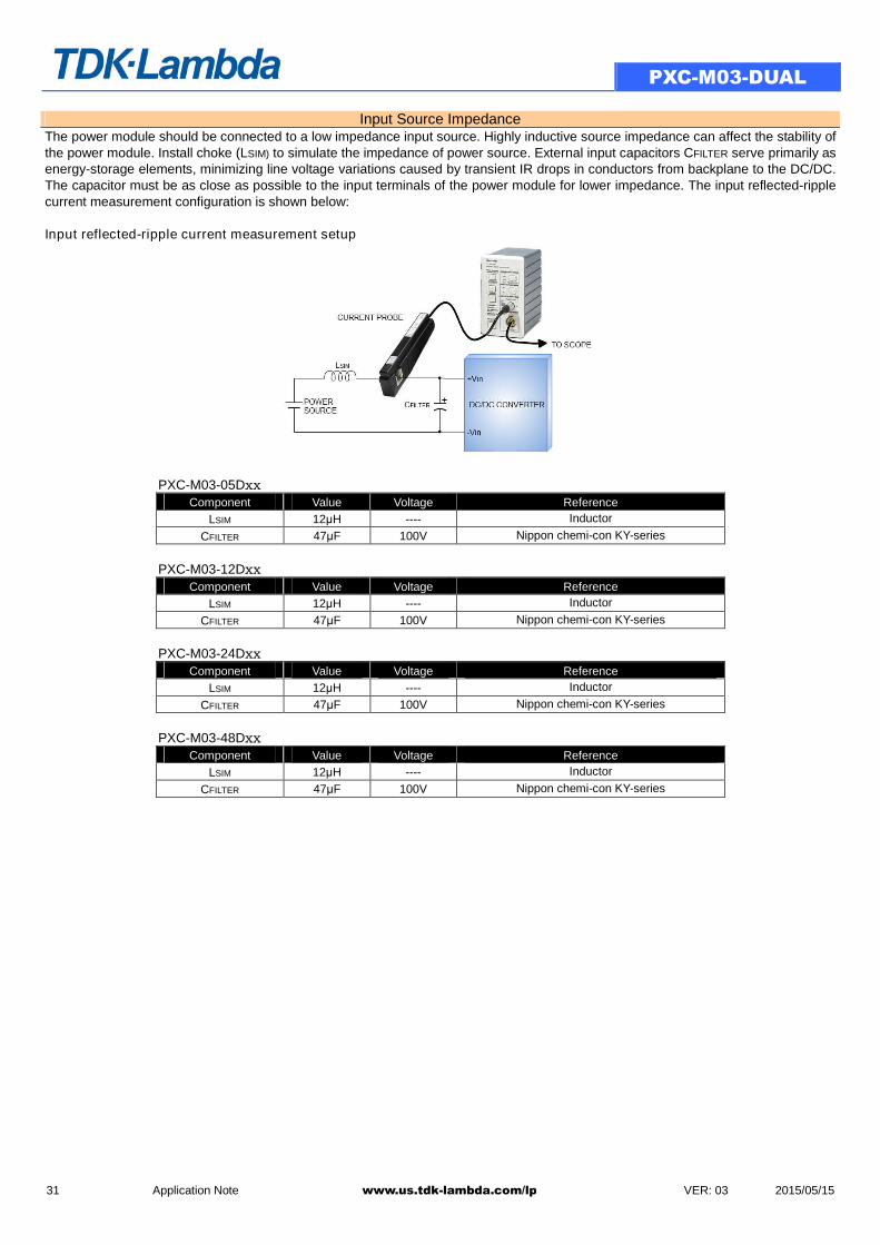
Input Source ImpedanceThe power module should be connected to a low impedance input source. Highly inductive source impedance can affect the stability ofthe power module. Install choke (LSIM) to simulate the impedance of power source. External input capacitors CFILTER serve primarily asenergy-storage elements, minimizing line voltage variations caused by transient IR drops in conductors from backplane to the DC/DC.The capacitor must be as close as possible to the input terminals of the power module for lower impedance. The input reflected-ripplecurrent measurement configuration is shown below:
Input reflected-ripple current measurement setup
PXC-M03-05Dxx
Component Value Voltage Reference
LSIM 12μH ---- Inductor
CFILTER 47μF 100V Nippon chemi-con KY-series
PXC-M03-12Dxx
Component Value Voltage Reference
LSIM 12μH ---- Inductor
CFILTER 47μF 100V Nippon chemi-con KY-series
PXC-M03-24Dxx
Component Value Voltage Reference
LSIM 12μH ---- Inductor
CFILTER 47μF 100V Nippon chemi-con KY-series
PXC-M03-48Dxx
Component Value Voltage Reference
LSIM 12μH ---- Inductor
CFILTER 47μF 100V Nippon chemi-con KY-series
PXC-M03-DUAL
32 Application Note www.us.tdk-lambda.com/lp VER: 03 2015/05/15
Output Over Current ProtectionWhen excessive output currents occur in the system, circuit protection is required on all power supplies. Normally, overload current ismaintained at approximately 150 percent of rated current for PXC-M03 SERIES.Hiccup-mode is a method of operation in a power supply whose purpose is to protect the power supply from being damaged during anover-current fault condition. It also enables the power supply to restart when the fault is removed. There are other ways of protecting thepower supply when it is over-loaded, such as the maximum current limiting or current fold-back methods.
One of the problems resulting from over current is that excessive heat may be generated in power devices; especially MOSFET andSchottky diodes and the temperature of those devices may exceed their specified limits. A protection mechanism has to be used toprevent those power devices from being damaged.
The operation of hiccup is as follows. When the current sense circuit sees an over-current event, the controller shuts off the powersupply for a given time and then tries to start up the power supply again. If the over-load condition has been removed, the power supplywill start up and operate normally; otherwise, the controller will see another over-current event and shut off the power supply again,repeating the previous cycle. Hiccup operation has none of the drawbacks of the other two protection methods, although its circuit ismore complicated because it requires a timing circuit. The excess heat due to overload lasts for only a short duration in the hiccupcycle, hence the junction temperature of the power devices is much lower.
The hiccup operation can be done in various ways. For example, one can start hiccup operation any time an over-current event isdetected; or prohibit hiccup during a designated start-up is usually larger than during normal operation and it is easier for anover-current event is detected; or prohibit hiccup during a designated start-up interval (usually a few milliseconds). The reason for thelatter operation is that during start-up, the power supply needs to provide extra current to charge up the output capacitor. Thus thecurrent demand during start-up is usually larger than during normal operation and it is easier for an over-current event to occur. If thepower supply starts to hiccup once there is an over-current, it might never start up successfully. Hiccup mode protection will give thebest protection for a power supply against over current situations, since it will limit the average current to the load at a low level, soreducing power dissipation and case temperature in the power devices.
Output Short Circuitry ProtectionContinuous and auto-recovery mode.
During short circuit, converter will shut down. The average current during this condition will be very low and the device is safe in thiscondition.
Output Over Voltage ProtectionThe output over-voltage protection consists of circuitry that internally clamps the output voltage. If a more accurate output over-voltageprotection scheme is required then this should be implemented externally via use of the remote on/off pin.
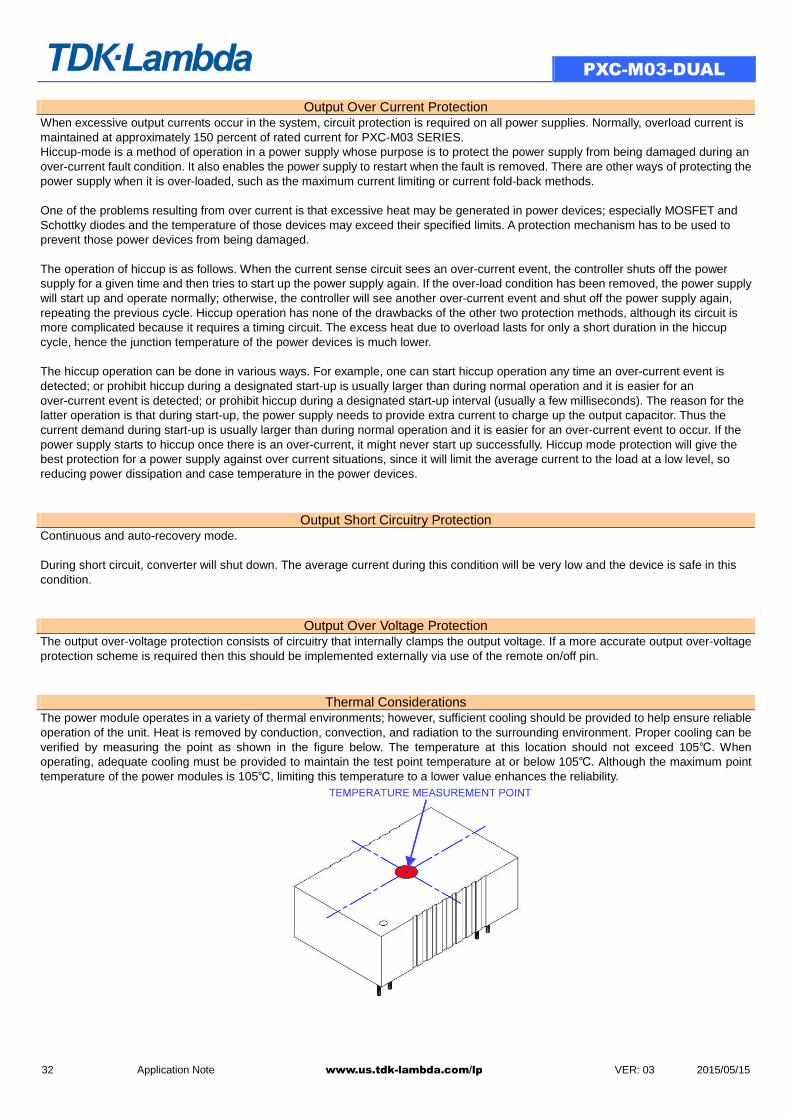
Thermal ConsiderationsThe power module operates in a variety of thermal environments; however, sufficient cooling should be provided to help ensure reliableoperation of the unit. Heat is removed by conduction, convection, and radiation to the surrounding environment. Proper cooling can beverified by measuring the point as shown in the figure below. The temperature at this location should not exceed 105℃. Whenoperating, adequate cooling must be provided to maintain the test point temperature at or below 105℃. Although the maximum pointtemperature of the power modules is 105℃, limiting this temperature to a lower value enhances the reliability.
PXC-M03-DUAL
33 Application Note www.us.tdk-lambda.com/lp VER: 03 2015/05/15
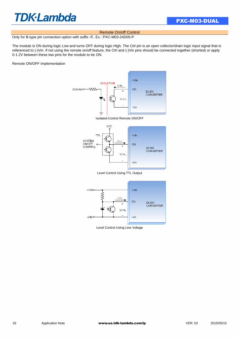
Remote On/off ControlOnly for B-type pin connection option with suffix -P,. Ex.: PXC-M03-24D05-P
The module is ON during logic Low and turns OFF during logic High. The Ctrl pin is an open collector/drain logic input signal that isreferenced to (-)Vin. If not using the remote on/off feature, the Ctrl and (-)Vin pins should be connected together (shorted) or apply0-1.2V between these two pins for the module to be ON.
Remote ON/OFF Implementation
Isolated-Control Remote ON/OFF
Level Control Using TTL Output
Level Control Using Line Voltage
PXC-M03-DUAL
34 Application Note www.us.tdk-lambda.com/lp VER: 03 2015/05/15
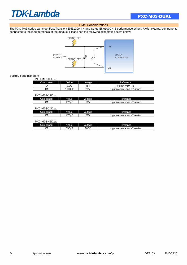
EMS ConsiderationsThe PXC-M03 series can meet Fast Transient EN61000-4-4 and Surge EN61000-4-5 performance criteria A with external componentsconnected to the input terminals of the module. Please see the following schematic shown below.
Surge / Fast TransientPXC-M03-05Dxx
Component Value Voltage Reference
D 10A 45V Vishay V10P45
C1 1000μF 25V Nippon chemi-con KY-series
PXC-M03-12DxxComponent Value Voltage Reference
C1 470μF 50V Nippon chemi-con KY-series
PXC-M03-24DxxComponent Value Voltage Reference
C1 470μF 50V Nippon chemi-con KY-series
PXC-M03-48DxxComponent Value Voltage Reference
C1 330μF 100V Nippon chemi-con KY-series
PXC-M03-DUAL
35 Application Note www.us.tdk-lambda.com/lp VER: 03 2015/05/15
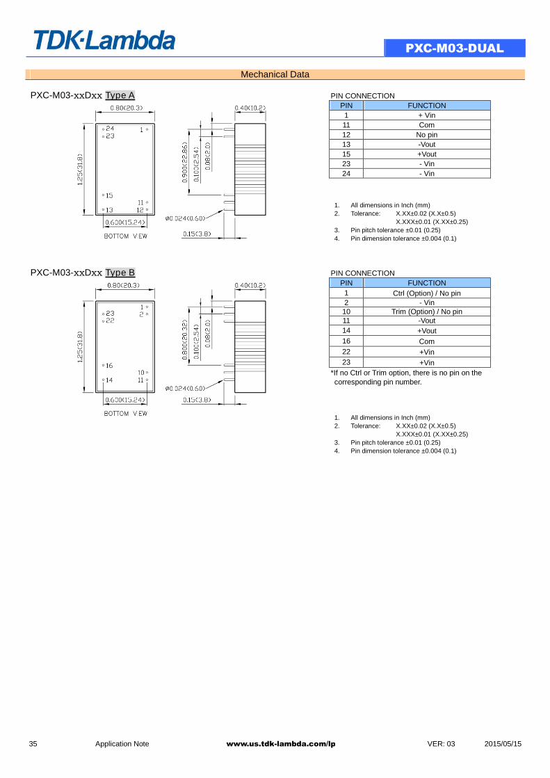
Mechanical Data
PXC-M03-xxDxx Type A
1. All dimensions in Inch (mm)
2. Tolerance: X.XX±0.02 (X.X±0.5)
X.XXX±0.01 (X.XX±0.25)
3. Pin pitch tolerance ±0.01 (0.25)
4. Pin dimension tolerance ±0.004 (0.1)
PIN CONNECTION
PIN FUNCTION
1 + Vin
11 Com
12 No pin
13 -Vout
15 +Vout
23 - Vin
24 - Vin
PXC-M03-xxDxx Type B
1. All dimensions in Inch (mm)
2. Tolerance: X.XX±0.02 (X.X±0.5)
X.XXX±0.01 (X.XX±0.25)
3. Pin pitch tolerance ±0.01 (0.25)
4. Pin dimension tolerance ±0.004 (0.1)
PIN CONNECTION
PIN FUNCTION
1 Ctrl (Option) / No pin
2 - Vin10 Trim (Option) / No pin11 -Vout
14 +Vout
16 Com
22 +Vin
23 +Vin
*If no Ctrl or Trim option, there is no pin on thecorresponding pin number.
PXC-M03-DUAL
36 Application Note www.us.tdk-lambda.com/lp VER: 03 2015/05/15
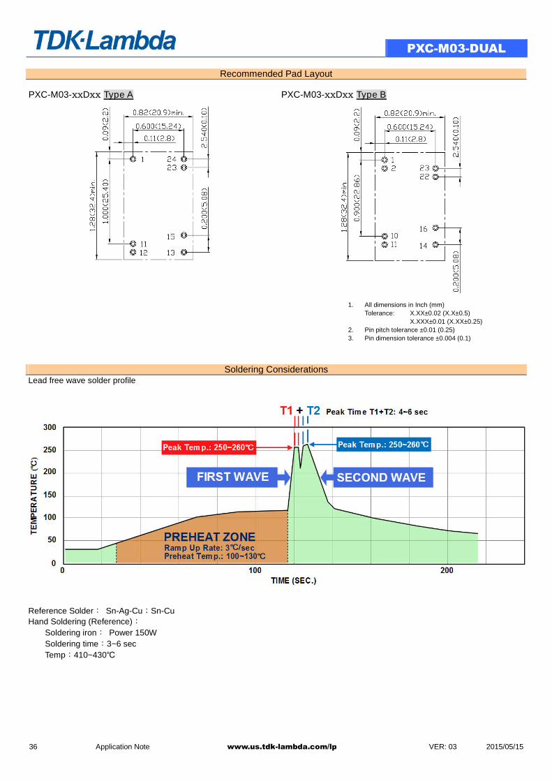
Recommended Pad Layout
PXC-M03-xxDxx Type A PXC-M03-xxDxx Type B
1. All dimensions in Inch (mm)
Tolerance: X.XX±0.02 (X.X±0.5)
X.XXX±0.01 (X.XX±0.25)
2. Pin pitch tolerance ±0.01 (0.25)
3. Pin dimension tolerance ±0.004 (0.1)
Soldering ConsiderationsLead free wave solder profile
Reference Solder: Sn-Ag-Cu;Sn-Cu
Hand Soldering (Reference):
Soldering iron: Power 150W
Soldering time:3~6 sec
Temp:410~430℃
PXC-M03-DUAL
37 Application Note www.us.tdk-lambda.com/lp VER: 03 2015/05/15
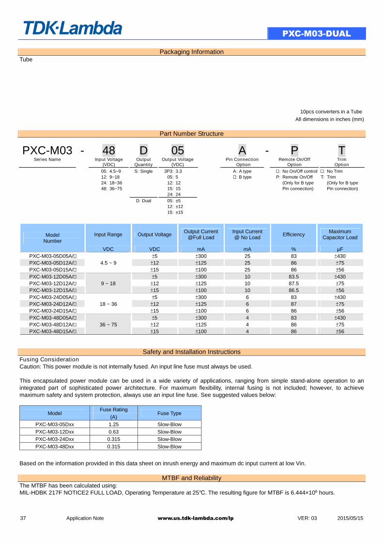
Packaging InformationTube
10pcs converters in a Tube
All dimensions in inches (mm)
Part Number Structure
PXC-M03 - 48 D 05 A - P TSeries Name Input Voltage
(VDC)Output
QuantityOutput Voltage
(VDC)Pin Connection
OptionRemote On/Off
OptionTrim
Option
05:
12:
24:
48:
4.5~9
9~18
18~36
36~75
S: Single 3P3:
05:
12:
15:
24:
3.3
5
12
15
24
A: A type
: B type
:
P:
No On/Off control
Remote On/Off
(Only for B type
Pin connection)
:
T:
No Trim
Trim
(Only for B type
Pin connection)
D: Dual 05:
12:
15:
±5
±12
±15
ModelNumber
Input Range Output VoltageOutput Current
@Full LoadInput Current@ No Load
EfficiencyMaximum
Capacitor Load
VDC VDC mA mA % μF
PXC-M03-05D05A/
4.5 ~ 9
±5 ±300 25 83 ±430
PXC-M03-05D12A/ ±12 ±125 25 86 ±75
PXC-M03-05D15A/ ±15 ±100 25 86 ±56
PXC-M03-12D05A/
9 ~ 18
±5 ±300 10 83.5 ±430
PXC-M03-12D12A/ ±12 ±125 10 87.5 ±75
PXC-M03-12D15A/ ±15 ±100 10 86.5 ±56
PXC-M03-24D05A/
18 ~ 36
±5 ±300 6 83 ±430
PXC-M03-24D12A/ ±12 ±125 6 87 ±75
PXC-M03-24D15A/ ±15 ±100 6 86 ±56
PXC-M03-48D05A/
36 ~ 75
±5 ±300 4 83 ±430
PXC-M03-48D12A/ ±12 ±125 4 86 ±75
PXC-M03-48D15A/ ±15 ±100 4 86 ±56
Safety and Installation InstructionsFusing ConsiderationCaution: This power module is not internally fused. An input line fuse must always be used.
This encapsulated power module can be used in a wide variety of applications, ranging from simple stand-alone operation to anintegrated part of sophisticated power architecture. For maximum flexibility, internal fusing is not included; however, to achievemaximum safety and system protection, always use an input line fuse. See suggested values below:
ModelFuse Rating
Fuse Type(A)
PXC-M03-05Dxx 1.25 Slow-Blow
PXC-M03-12Dxx 0.63 Slow-Blow
PXC-M03-24Dxx 0.315 Slow-Blow
PXC-M03-48Dxx 0.315 Slow-Blow
Based on the information provided in this data sheet on inrush energy and maximum dc input current at low Vin.
MTBF and ReliabilityThe MTBF has been calculated using:MIL-HDBK 217F NOTICE2 FULL LOAD, Operating Temperature at 25℃. The resulting figure for MTBF is 6.444×10⁶ hours.