Embed Size (px)
Citation preview

PWB Back Drilling Failure Analysis
Members Meeting Sept 25-26, 2013
Bennington, Vermont
Project Lead: TBA
Project Proposal -Definition Stage
© 2013 HDP User Group International, Inc. All rights reserved 1

Backdrill Description
Backdrilling or Controlled
Depth Drilling is the
removal of the plated
copper in the PTH by a
secondary drilling process.
The purpose of this process
is to reduce the extraneous
via length in high speed
circuits to reduce reflection
and increase signal
integrity.
The critical parameter is the
length of remaining copper
via (Stub) from the targeted
inner layer pad © 2013 HDP User Group International, Inc. All rights reserved
2

Project Background
• Back drilling or controlled depth drilling of plated
through holes (PTH) is increasingly being used in
High Speed Designs.
• While back drilling of PWBs helps to remove
signal distortion by removing via related stubs,
reliability issues attributed to this practice appear
to be on the rise.
© 2013 HDP User Group International, Inc. All rights reserved 3
Project Drivers/Gaps/Purpose
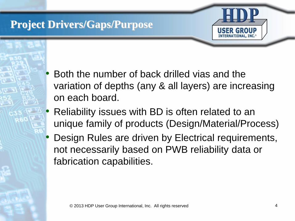
• Both the number of back drilled vias and the
variation of depths (any & all layers) are increasing
on each board.
• Reliability issues with BD is often related to an
unique family of products (Design/Material/Process)
• Design Rules are driven by Electrical requirements,
not necessarily based on PWB reliability data or
fabrication capabilities.
© 2013 HDP User Group International, Inc. All rights reserved 4
Increase usage of Back Drilling
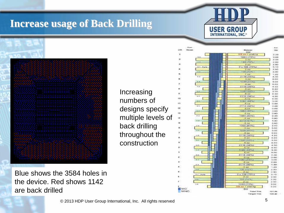
Blue shows the 3584 holes in
the device. Red shows 1142
are back drilled
Increasing
numbers of
designs specify
multiple levels of
back drilling
throughout the
construction
© 2013 HDP User Group International, Inc. All rights reserved 5
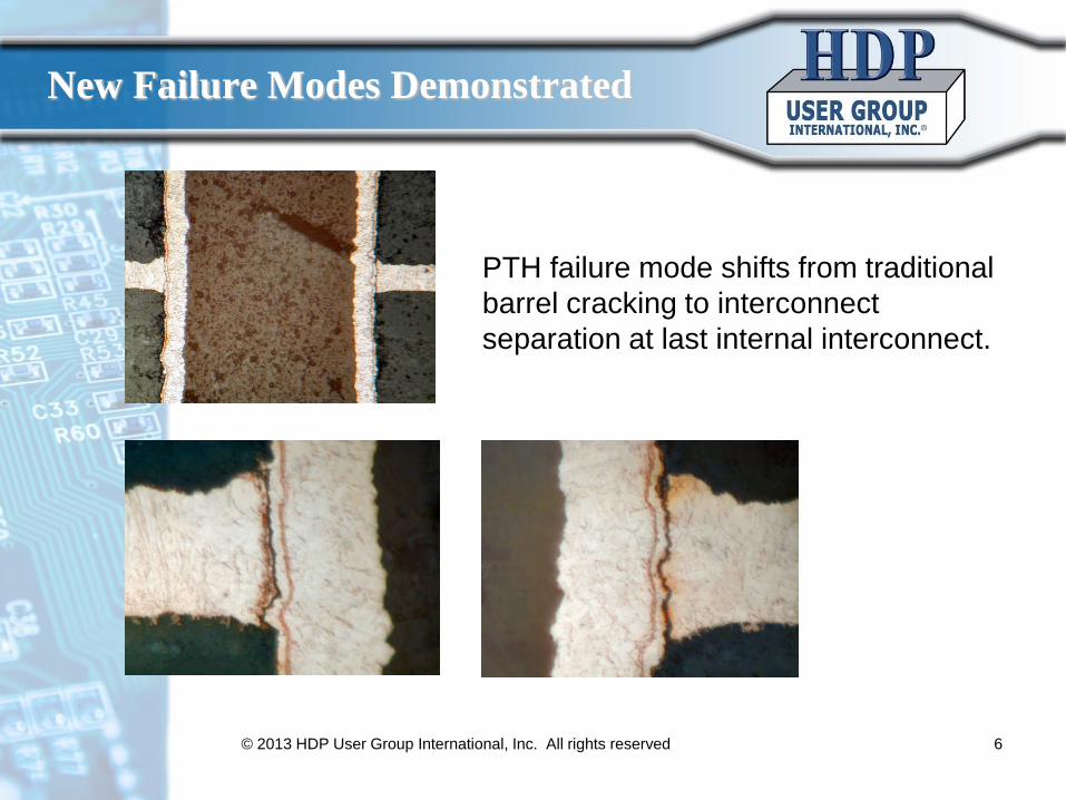
New Failure Modes Demonstrated
PTH failure mode shifts from traditional
barrel cracking to interconnect
separation at last internal interconnect.
© 2013 HDP User Group International, Inc. All rights reserved 6

Project Challenges
• Confirming/Quantifying Back Drill Depth
Control and Cleanliness of Back Drilled Hole
• Specification of Tolerances
• Documenting OEM/ODM Requirements
• Documenting PWB Fabricator Concerns
• Quantifying the Impact of Copper Foil
Thickness
• Reliability or “Surviving” Lead Free Assembly
and/or Rework
• Analyzing new failure modes w/ Backdrilling
© 2013 HDP User Group International, Inc. All rights reserved 7
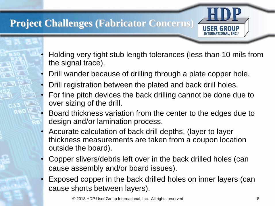
Project Challenges (Fabricator Concerns)
• Holding very tight stub length tolerances (less than 10 mils from the signal trace).
• Drill wander because of drilling through a plate copper hole.
• Drill registration between the plated and back drill holes.
• For fine pitch devices the back drilling cannot be done due to over sizing of the drill.
• Board thickness variation from the center to the edges due to design and/or lamination process.
• Accurate calculation of back drill depths, (layer to layer thickness measurements are taken from a coupon location outside the board).
• Copper slivers/debris left over in the back drilled holes (can
cause assembly and/or board issues).
• Exposed copper in the back drilled holes on inner layers (can
cause shorts between layers).
© 2013 HDP User Group International, Inc. All rights reserved 8
Project Objectives
• This project aims to explore the reason for back
drilling related PWB failures and to identify
potential solutions and design/process guidelines
to prevent future problems associated with this
process.
• This will be accomplished in 3 proposed phases
– Phase 1: Survey
– Phase 2: Reliability testing
– Phase 3: Guideline documentation
© 2013 HDP User Group International, Inc. All rights reserved 9
Project Scope: Three Phase Project
• Phase 1: Assessing the backdrill situation in the
Industry through a 1:1 survey. All inputs will be
company coded to keep all data anonymous.
– Part 1: OEM/ODM Survey to document what design
tolerances/stub lengths are being designed into
products now and 3 years into the future.
– Part 2. PWB Fabricator Survey to document what
problems manufacturers see in supporting the level of
technology/tolerance and what would be needed to
comply with the requirements.
© 2013 HDP User Group International, Inc. All rights reserved 10

Project Scope: Three Phase Project
• Phase 2: Test and verify the reliability and
capabilities discovered in the Phase 1 surveys.
This will be done by designing an electrically
tested coupon (IST) and test vehicle that will be
built and tested by the project. (micro-sectioning
only as needed)
• Phase 3: Develop a realistic set of design
guidelines for several levels of PWB Fabrication
capabilities (cutting edge and mainstream
fabricators).
© 2013 HDP User Group International, Inc. All rights reserved 11

Project Scope: Three Phase Project
Examples of OEM/ODM Survey questions:• Are you designing with backdrilled subpanels or sub-laminations?
• Are you BD drilling from both sides of the panel?
• How many depths or levels do you drill on a panel?
• How dense is the backdrill area (BD per cm2)?
• What pitch are you Backdrilling? (Ex: 1mm pitch typical to .4mm
cutting edge)?
• What size of over-drill do you design for? (Ex: initial drill + XX mils)
• What is the limit by design on the minimum stub length removal?
(What length of via would you not remove?)
• Do you know of any specific designs that have given the industry
trouble with BD fabrication?
• Do you know of any specific designs that have given the industry
trouble with reliability of BD?
© 2013 HDP User Group International, Inc. All rights reserved 12
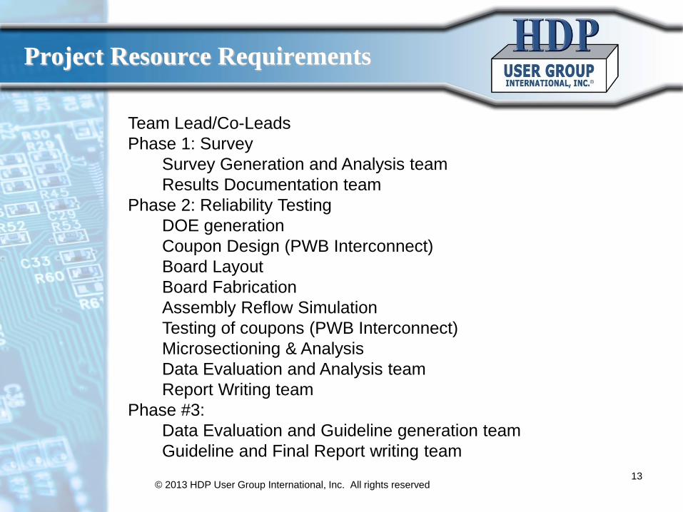
Project Resource Requirements
Team Lead/Co-Leads
Phase 1: Survey
Survey Generation and Analysis team
Results Documentation team
Phase 2: Reliability Testing
DOE generation
Coupon Design (PWB Interconnect)
Board Layout
Board Fabrication
Assembly Reflow Simulation
Testing of coupons (PWB Interconnect)
Microsectioning & Analysis
Data Evaluation and Analysis team
Report Writing team
Phase #3:
Data Evaluation and Guideline generation team
Guideline and Final Report writing team
© 2013 HDP User Group International, Inc. All rights reserved13
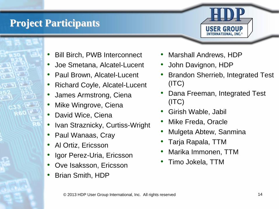
Project Participants
• Bill Birch, PWB Interconnect
• Joe Smetana, Alcatel-Lucent
• Paul Brown, Alcatel-Lucent
• Richard Coyle, Alcatel-Lucent
• James Armstrong, Ciena
• Mike Wingrove, Ciena
• David Wice, Ciena
• Ivan Straznicky, Curtiss-Wright
• Paul Wanaas, Cray
• Al Ortiz, Ericsson
• Igor Perez-Uria, Ericsson
• Ove Isaksson, Ericsson
• Brian Smith, HDP
• Marshall Andrews, HDP
• John Davignon, HDP
• Brandon Sherrieb, Integrated Test
(ITC)
• Dana Freeman, Integrated Test
(ITC)
• Girish Wable, Jabil
• Mike Freda, Oracle
• Mulgeta Abtew, Sanmina
• Tarja Rapala, TTM
• Marika Immonen, TTM
• Timo Jokela, TTM
© 2013 HDP User Group International, Inc. All rights reserved 14
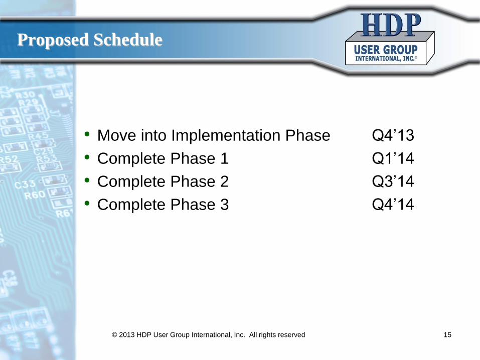
Proposed Schedule
• Move into Implementation Phase Q4’13
• Complete Phase 1 Q1’14
• Complete Phase 2 Q3’14
• Complete Phase 3 Q4’14
© 2013 HDP User Group International, Inc. All rights reserved 15


![PWB Handbook[1]](https://img.pdfslide.us/doc/110x75/577d25b71a28ab4e1e9f734a/pwb-handbook1.jpg)