Embed Size (px)
Citation preview
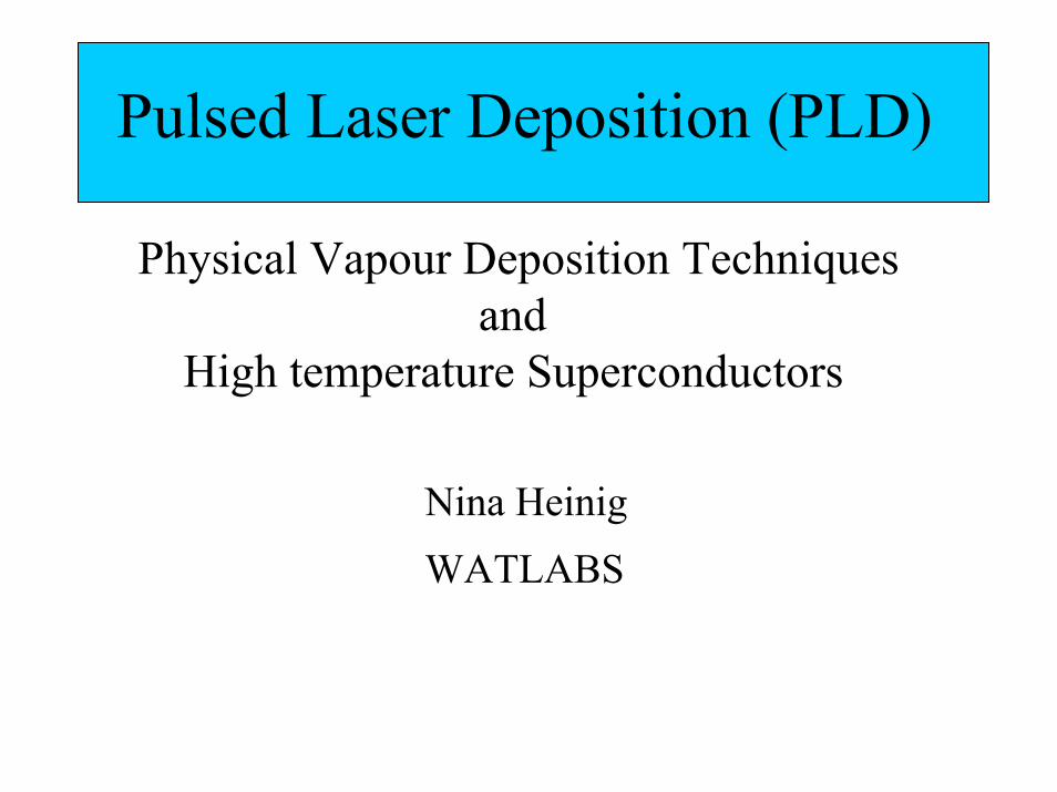
Pulsed Laser Deposition (PLD)
Physical Vapour Deposition Techniquesand
High temperature Superconductors
Nina HeinigWATLABS
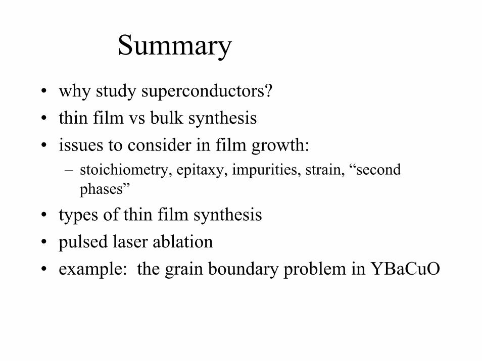
Summary• why study superconductors?• thin film vs bulk synthesis• issues to consider in film growth:
– stoichiometry, epitaxy, impurities, strain, “second phases”
• types of thin film synthesis• pulsed laser ablation• example: the grain boundary problem in YBaCuO
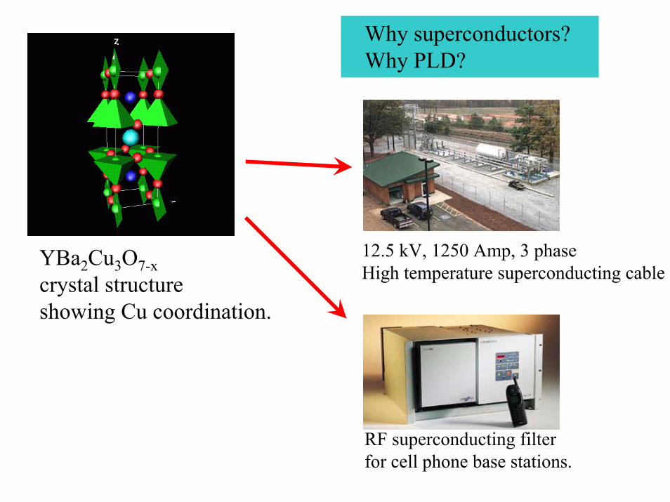
12.5 kV, 1250 Amp, 3 phaseHigh temperature superconducting cable
RF superconducting filterfor cell phone base stations.
YBa2Cu3O7-xcrystal structureshowing Cu coordination.
Why superconductors?Why PLD?
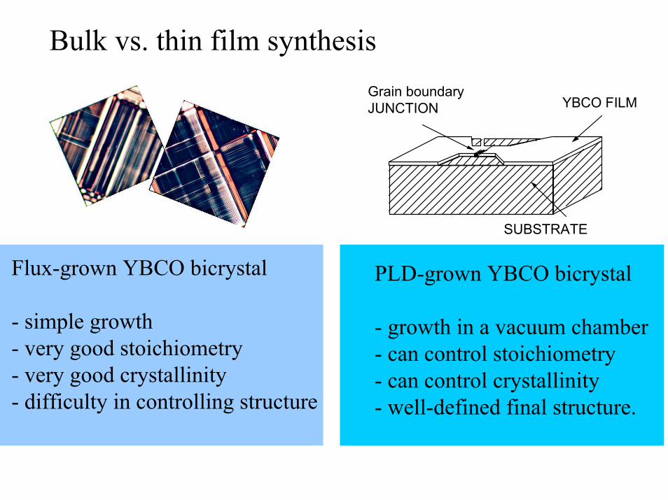
Bulk vs. thin film synthesis
YBCO FILMGrain boundaryJUNCTION
SUBSTRATE
Flux-grown YBCO bicrystal
- simple growth- very good stoichiometry- very good crystallinity- difficulty in controlling structure
PLD-grown YBCO bicrystal
- growth in a vacuum chamber- can control stoichiometry- can control crystallinity- well-defined final structure.
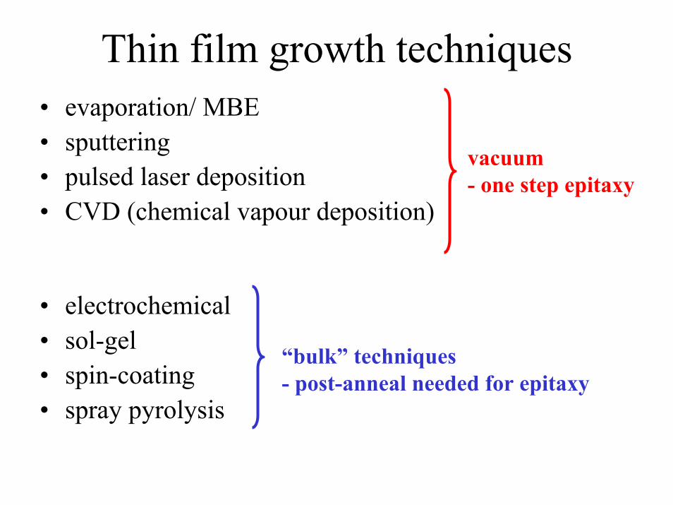
Thin film growth techniques• evaporation/ MBE• sputtering • pulsed laser deposition• CVD (chemical vapour deposition)
• electrochemical• sol-gel• spin-coating• spray pyrolysis
vacuum- one step epitaxy
“bulk” techniques- post-anneal needed for epitaxy
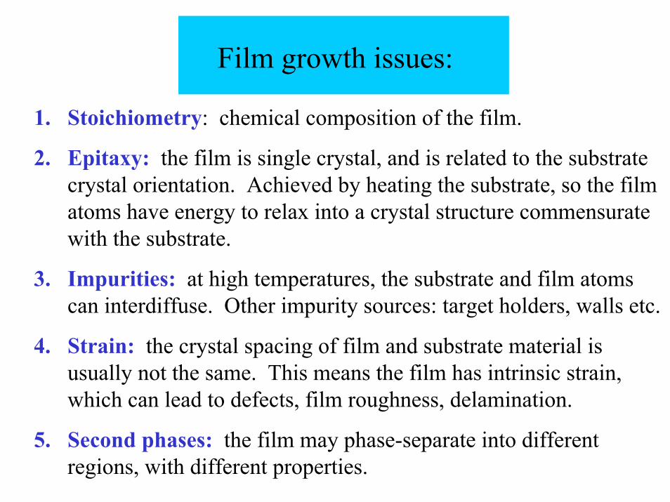
Film growth issues:
1. Stoichiometry: chemical composition of the film.
2. Epitaxy: the film is single crystal, and is related to the substrate crystal orientation. Achieved by heating the substrate, so the film atoms have energy to relax into a crystal structure commensuratewith the substrate.
3. Impurities: at high temperatures, the substrate and film atoms can interdiffuse. Other impurity sources: target holders, walls etc.
4. Strain: the crystal spacing of film and substrate material is usually not the same. This means the film has intrinsic strain,which can lead to defects, film roughness, delamination.
5. Second phases: the film may phase-separate into different regions, with different properties.
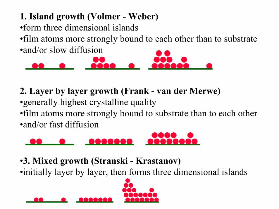
1. Island growth (Volmer - Weber)•form three dimensional islands •film atoms more strongly bound to each other than to substrate •and/or slow diffusion
2. Layer by layer growth (Frank - van der Merwe)•generally highest crystalline quality •film atoms more strongly bound to substrate than to each other •and/or fast diffusion
•3. Mixed growth (Stranski - Krastanov)•initially layer by layer, then forms three dimensional islands
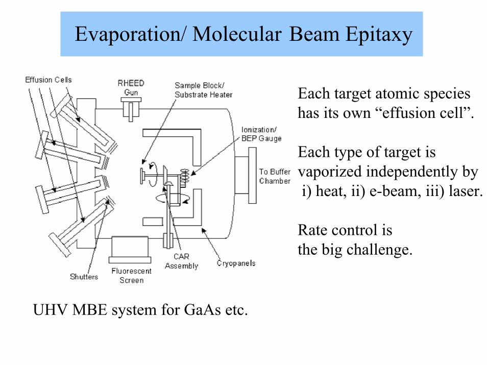
Evaporation/ Molecular Beam Epitaxy
Each target atomic specieshas its own “effusion cell”.
Each type of target is vaporized independently byi) heat, ii) e-beam, iii) laser.
Rate control is the big challenge.
UHV MBE system for GaAs etc.
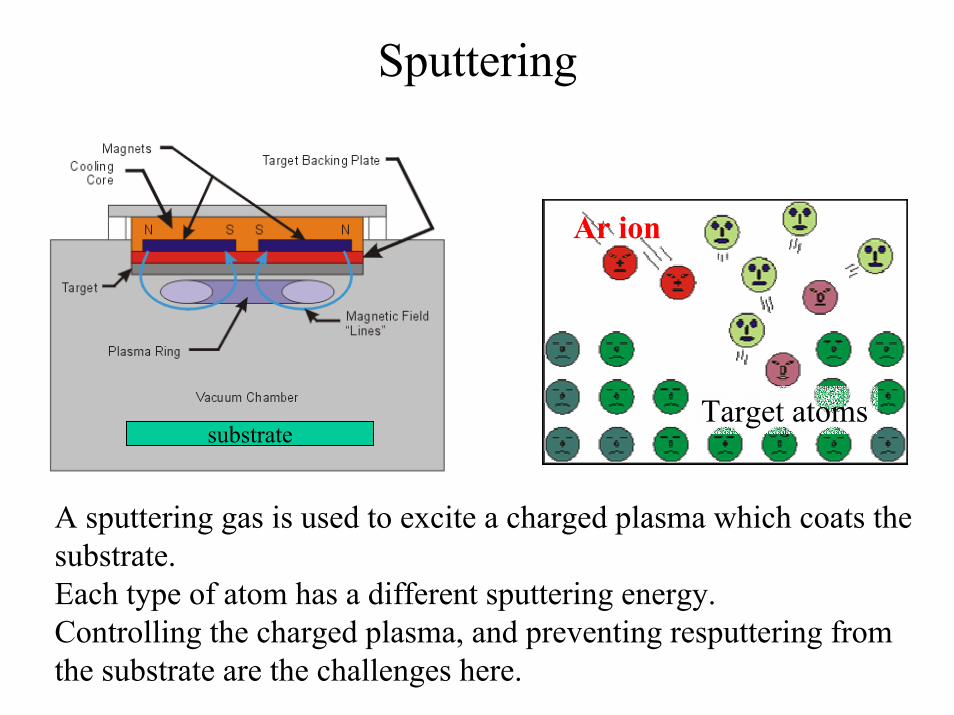
Sputtering
Ar ion
Target atomssubstrate
A sputtering gas is used to excite a charged plasma which coats the substrate.Each type of atom has a different sputtering energy.Controlling the charged plasma, and preventing resputtering from the substrate are the challenges here.
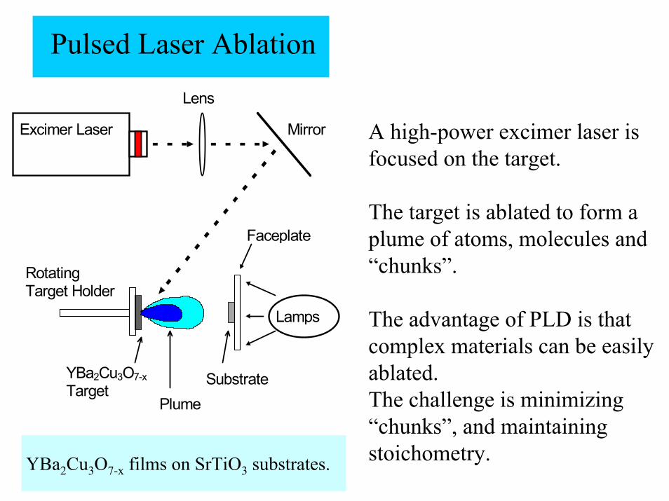
YBa2Cu3O7-x films on SrTiO3 substrates.
Lamps
RotatingTarget Holder
Excimer Laser Mirror
Lens
YBa2Cu3O7-xTarget
SubstratePlume
Faceplate
Pulsed Laser Ablation
A high-power excimer laser is focused on the target.
The target is ablated to form a plume of atoms, molecules and“chunks”.
The advantage of PLD is that complex materials can be easilyablated.The challenge is minimizing “chunks”, and maintaining stoichometry.
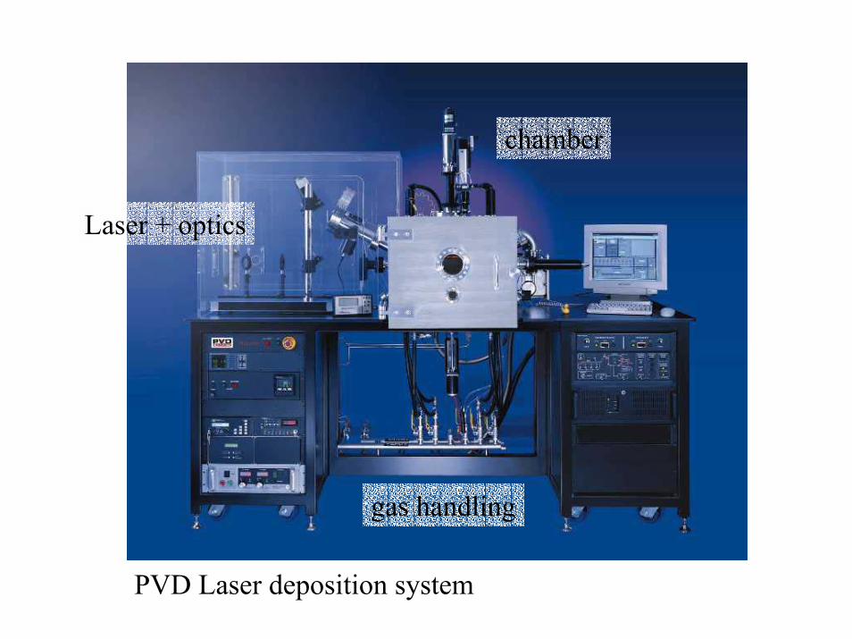
Laser + optics
gas handling
chamber
PVD Laser deposition system
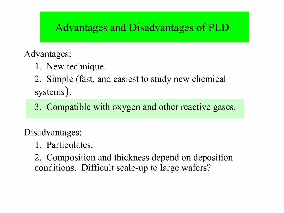
Advantages and Disadvantages of PLD
Advantages:1. New technique.2. Simple (fast, and easiest to study new chemical systems).3. Compatible with oxygen and other reactive gases.
Disadvantages:1. Particulates.2. Composition and thickness depend on deposition conditions. Difficult scale-up to large wafers?
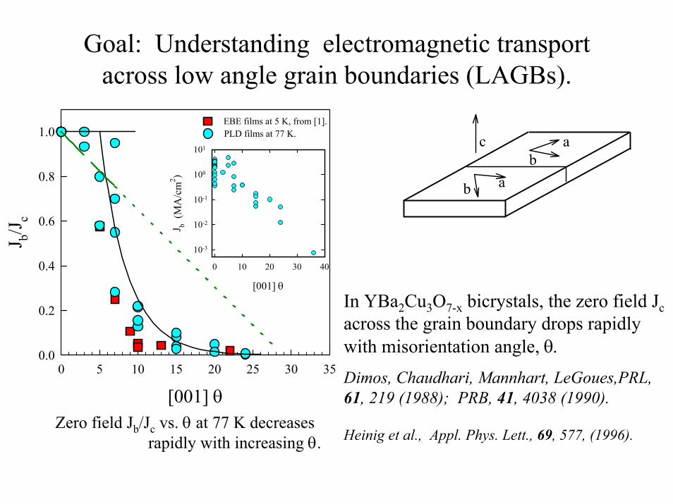
Goal: Understanding electromagnetic transportacross low angle grain boundaries (LAGBs).
[001] θ0 5 10 15 20 25 30 35
J b/Jc
0.0
0.2
0.4
0.6
0.8
1.0EBE films at 5 K, from [1].PLD films at 77 K.
[001] θ
0 10 20 30 40
J b (M
A/c
m2 )
10-3
10-2
10-1
100
101
ab
c a
b
In YBa2Cu3O7-x bicrystals, the zero field Jcacross the grain boundary drops rapidly with misorientation angle, θ.
Dimos, Chaudhari, Mannhart, LeGoues,PRL,61, 219 (1988); PRB, 41, 4038 (1990).
Heinig et al., Appl. Phys. Lett., 69, 577, (1996).Zero field Jb/Jc vs. θ at 77 K decreases
rapidly with increasing θ.
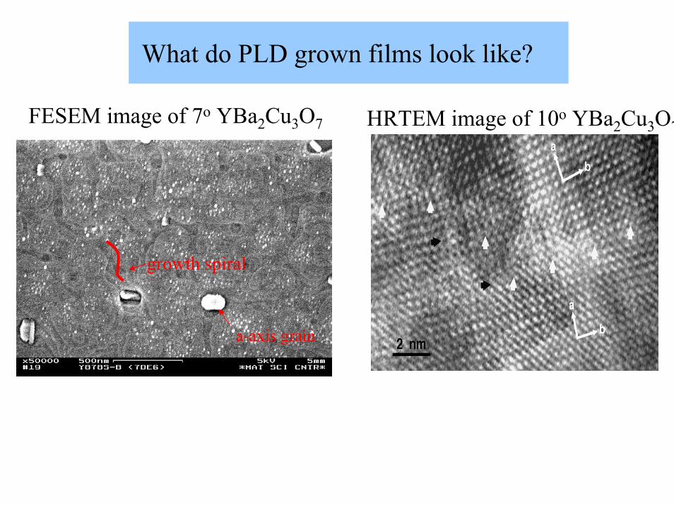
What do PLD grown films look like?
FESEM image of 7o YBa2Cu3O7 HRTEM image of 10o YBa2Cu3O7
a-axis grain
growth spiral
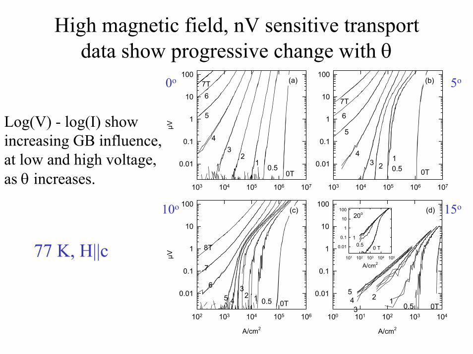
High magnetic field, nV sensitive transport data show progressive change with θ
(d)
103 104 105 106 107
µV0.01
0.1
1
10
1007T
0T
6
0.51
23
4
5
103 104 105 106 107
0.01
0.1
1
10
100
7T
6
5
43 2 0.5
1
0T
A/cm2
102 103 104 105 106
µV
0.01
0.1
1
10
100
8T
7
6
5 4
32 1 0.5 0T
A/cm2
100 101 102 103 104
0.01
0.1
1
10
100
5
34 2 1
0.5 0T
A/cm2101 102 103 104 105
0.01
0.1
1
10
100(c)
(b)(a)
20o
0 T0.51
0o
10o
5o
15o
Log(V) - log(I) show increasing GB influence, at low and high voltage,as θ increases.
77 K, H||c
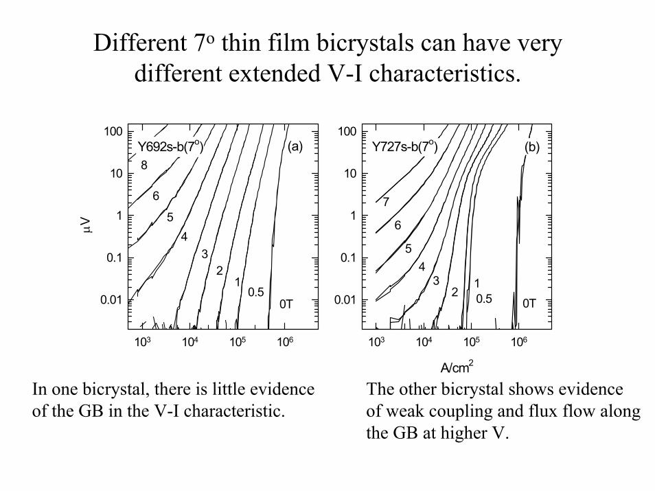
Different 7o thin film bicrystals can have very different extended V-I characteristics.
A/cm2
103 104 105 106
0.01
0.1
1
10
100
103 104 105 106
µV
0.01
0.1
1
10
100Y692s-b(7o) Y727s-b(7o)(a) (b)
0T0.5
12
34
5
6
8
0T0.51
23
45
6
7
In one bicrystal, there is little evidenceof the GB in the V-I characteristic.
The other bicrystal shows evidenceof weak coupling and flux flow along the GB at higher V.
• Low angle [001] tilt YBa2Cu3O7-x bicrystals were grown by laser ablation, and characterized byFESEM, TEM, and zero and high magnetic field transport.
• A progression from strongly coupled, flux-pinning limited transport behavior to weakly coupled, Josephson behavior was seen between 3o and 15o.
• Variation between bicrystals with the same θ shows that extrinsic factors modify the GB transition region.
Acknowledgments
Ron Redwing, George Daniels, J.E. Nordman,A.A. Polyanskii, A.E. Pashitski, A. Gurevich,
I-Fei Tsu, S.E. Babcock,D.C. Larbalestier
Work supported by NSF-MRSEC and EPRI
University of WisconsinUniversity of Wisconsin--MadisonMadisonApplied Superconductivity CenterApplied Superconductivity Center
![MAGRASO-70x100 [Modo de compatibilidad] - UCMwebs.ucm.es/centros/cont/descargas/documento40780.pdf(BZY) by pulsed laser deposition (PLD) on standard single crystal substrates (MgO,](https://img.pdfslide.us/doc/110x75/5e7101c3fb685f00716e0cea/magraso-70x100-modo-de-compatibilidad-bzy-by-pulsed-laser-deposition-pld.jpg)


![pH effects on novel SERS active substrateswwgis.ipcf.cnr.it/poster/3.pdf · Gold and Silver Nanoparticles obtained from Pulsed Laser Deposition (PLD)[1-3] have been deposited on glass](https://img.pdfslide.us/doc/110x75/5e71059ae508f45e976bcfed/ph-effects-on-novel-sers-active-gold-and-silver-nanoparticles-obtained-from-pulsed.jpg)