Embed Size (px)
Citation preview
PULSE AND DIGITALCIRCUITS
(AEC006)II-B.Tech IV- Sem-ECE
(R16 Regulation)
Mr.B.Naresh
Asso.Prof
Prepared by
Mrs.J.Sravana
Asst.Prof
Mrs.N. Anusha
Asst.Prof
Mrs.P. Saritha
Asso.Prof
1
UNIT-1
WAVESHAPING CIRCUITS
2

Basics
• Most natural quantities that we see are analog and vary continuously. Analog systems can generally handle higher power than digital systems
Temperature
(F)
100
95
90
85
80
75
70
1 2 3 4 5 6 7 8 9 10 11 12 1 2 3 4 5 6 7 8 9 10 11 12Time ofday
• Digital systems can Ap.Mr.ocess, store, anP.Md. transmit data more
efficiently but can only assign discrete values to eachpoint
Analog Quantities
3

Analog and Digital Systems
• Digital systems can process, store, and transmit data more
efficiently but can only assign discrete values to eachpoint
CDdrive
Soun
d
waves
10110011101
Digital data
Digital-to-
analog
converter
LinearamplifierAnalog
reproduction
ofmusic
audio signalSpeaker
4

Contd..
• Digital electronics uses circuits that have two states, which are represented by two different voltage levels called HIGH and LOW. The voltages represent numbers in the binary system
• In binary, a single number is called a bit (for binary digit). A bit can have the value of either a 0 or a 1, depending on if the
5

Digital Signals
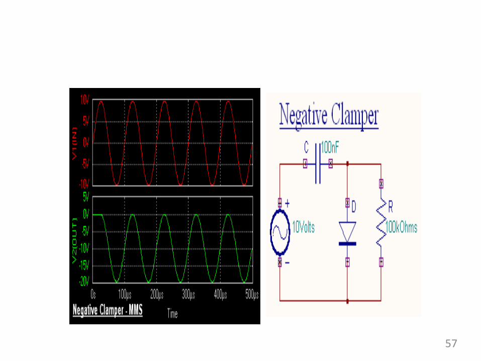
• Digital waveforms change between the LOW and HIGH
levels. A positive going pulse is one that goes from anormally
LOW logic level to a HIGH level and then back again. Digital
waveforms are made up of a series of pulses
HIGH HIGH
FallingorRisingor
leadingedge
Falling or
trailing
edge
leadingedgeRising or
trailing edge
LOWt0 t1
LOWt0 t1
(a)Positive–goingpulse (b)Negative–goingpulse
6
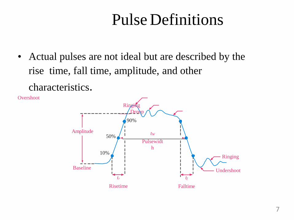
Pulse Definitions
• Actual pulses are not ideal but are described by the
rise time, fall time, amplitude, and other
characteristics.Overshoot
Ringing
Droop
90%
Amplitude50%
tW
Pulsewidt
h10%
Baseline
tftr
Risetime Falltime
Ringing
Undershoot
7

Periodic Pulse Waveforms
• Periodic pulse waveforms are composed of pulses that repeats in a fixed interval called the period.
• The frequency is the rate it repeats and ismeasured in hertz. The clock is a basic timingsignal that is an example of a periodic wave.
•
T 1 z
f
What is the period of a repetitive wave if f = 3.2 GHz?
8

Pulse width(tW)
Pulse Definitions
• In addition to frequency and period, repetitive pulse
waveforms are described by the amplitude (A), pulse
width (tW) and duty cycle. Duty cycle is the ratio of tW to
T.
Volts
Amplitude
Time
Period,T
9

Wave Shaping
Definition: It is the process of changing the
shape of input signal with linear / non-linear
circuits.
Types:
i.Linear Wave Shaping ii.Non-linear Wave
Shaping
10

Linear WaveShaping
Definition: The process where by the form of a non-sinusoidal signal is changed by transmission through a linear network is called Linear Wave Shaping.
Types:
i.High Pass RC Circuit. ii.Low Pass RC Circuit.
11
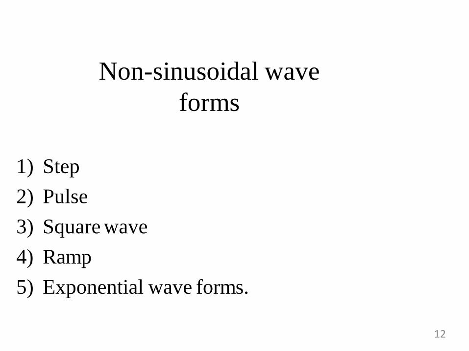
Non-sinusoidal wave
forms
1) Step
2) Pulse
3) Square wave
4) Ramp
5) Exponential wave forms.
12
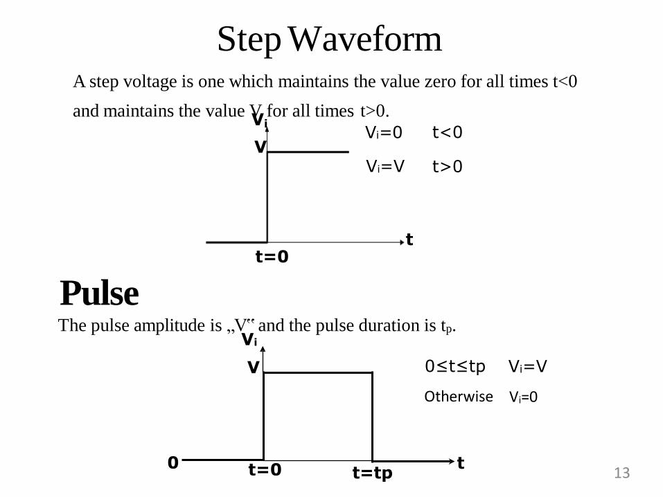
Step WaveformA step voltage is one which maintains the value zero for all times t<0
and maintains the value V for all times t>0.
Vi=0Vi
Vt<0
Vi=V t>0
Pulse
tt=0
The pulse amplitude is „V‟ and the pulse duration is tp.Vi
V
0 t=0
0≤t≤tp
Otherwise
t=tpt
Vi=V
Vi=0
13

SquareWave• A wave form which maintains itself at one constant level v1 for a time T1
and at other constant Level V11 for a time T2 and which is repetitive witha period T=T1+T2 is called a square-wave.
t
T1 T2
RampA waveform which is zero for t<0 and which increases linearly with time for t>0.
Vi
Vi =αt
Vi =αt , t>0
014

0
Exponential
• The exponential waveform input is givenby
where T is the time constant of the exponential input
Vi
V
t
15

High Pass RC Circuit
C+ +
ViR Vo
--
If f=low, Xc becomeshigh
XC1
2fC
C act as open circuit, so theVo=0.
If f=high, Xc becomes low
C acts as short circuit, so we get the output.
Thehigher frequency componentsin the input signal appear at
the output with less attenuation due to this
behavior the circuit is called “High Pass Filter”.16

Sinusoidal input
• For Sinusoidal input, the output increases in
amplitude with increasing frequency.
i=Vin
Vo= iR
= Vin
+C
+
Vini R
V
R - jXC R - j
2πfC _ _ O
i=Vin
j R 1-
OV =iR=
2πfRC
Vin×R j =
Vinj1-
2πRfR1C- 2πfRC
17
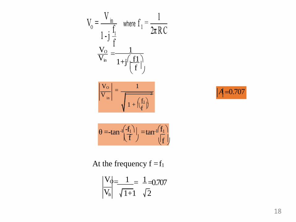
f
=1VO
Vin 1+j-f1
VO=
Vin
1 = 1 =0.707
1+1 2
VO 1
V=
2
in f1
1 + f
A 0.707
θ =-tan -1-f1 =tan-1f1 f f
At the frequency f =f1
18

At f = f1 the gain is 0.707 or this level corresponds to a signal reduction of 3
decibels(dB).
f1 is referred to as Lower 3-dB frequency.
19

1 1
2 2
Square wave input
• Percentage Tilt ( 0 0 Tilt)
Tilt is defined as the decay in the amplitude of the output voltage wave
due to the input voltage maintaining constant level
V '- T 1
= V . e R C (1)
V'= V
-T 2
. e RC
'1 2
1
(2)
(3)
(4)
P V V1
11
VX100
2
V - V = V
V - V ' = V2
20
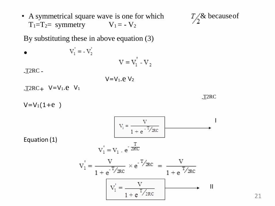
& becauseof• A symmetrical square wave is one for which T1=T2= symmetry V1 = - V2
-T2RC+ V=V1.e V1
V=V1(1+e )
By substituting these in above equation (3)
•
-T2RC -
V=V1.e V2
-T2RC
I
Equation (1)
II
21

ForRC>>Ttheequation(I)&(I)becomesas
1
2
V V (1+ )&V1V
(1-T T
)1
2 4RC 2
Thepercentagetilt‘P’isdefinedbyP=V
4RCV1-V
1
12
100
22

High Pass RC circuit acts as
differentiator:-• The time constant of high pass RC circuit in very small in comparison
within the time required for the input signal to make an appreciable change, the circuit is called a “differentiator”.
• Under this circumstances the voltage drop across R will be very small in comparison with the drop across C. Hence we may consider that the total input Vi appears across C, so that the current is determined entirely by the capacitance.
• Then the current is i = Cand the output signal across R is V0 = iR
V0 = RC
• hence the output is proportional to the derivative of the input.
23
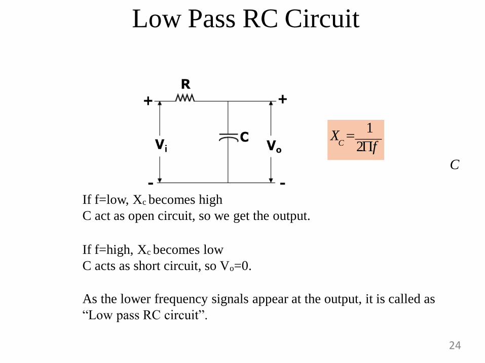
Low Pass RC Circuit
C
If f=low, Xc becomes high
C act as open circuit, so we get the output.
If f=high, Xc becomes low
C acts as short circuit, so Vo=0.
As the lower frequency signals appear at the output, it is called as
“Low pass RC circuit”.
X C
1
2f
24
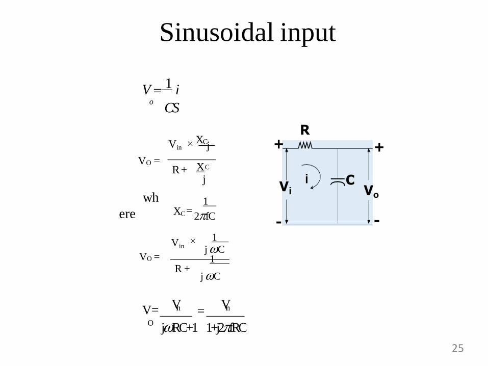
1
Sinusoidal input
V 1 io
CS
Vin × XCj
VO =R+ XC
j
wh
ere1
XC = 2fC
VO =
Vin×
jC1
R +jC
=Vin VinV=
OjRC+1 1+j2fRC
25

θ=- tan -1 f
f2
OV=Vin
1+ j fwhere f =
2
1
2RC= 1
1 +jf
f2
and
At the frequency f =f2
VO= 1 = 1 =0.707
Vin 1+1 2
A 0.707
A = 12
1+ f f2
f2
A = VO
Vin
26

At f = f2 the gain is 0.707 or this level corresponds to a signal reduction of 3
decibels(dB).
f2 or fh is referred to as upper 3-dBfrequency.
27
Square wave input
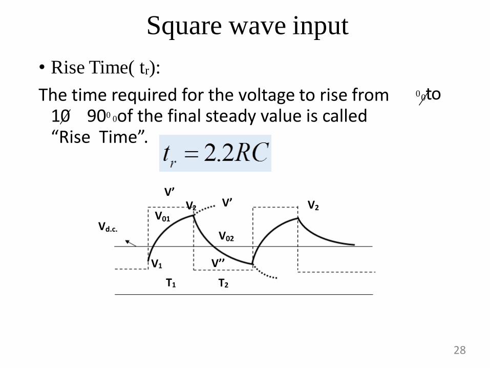
• Rise Time( tr):
The time required for the voltage to rise from 10 900 0of the final steady value is called “Rise Time”.
00to
Vd.c.
V’V2
V01
V’ V2
V02
V1
T1
V’’
T2
28
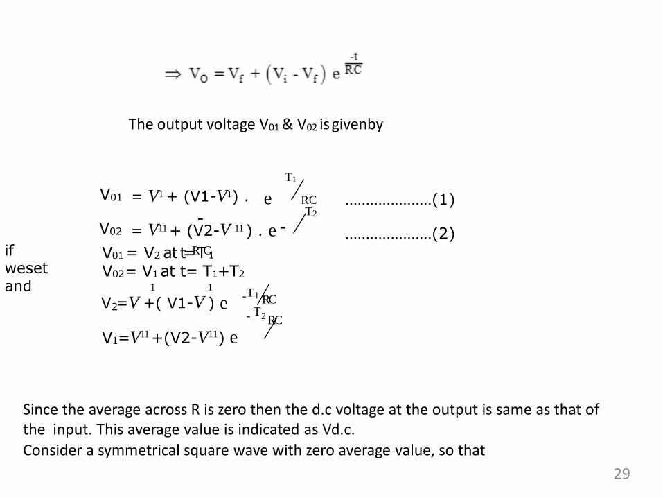
The output voltage V01 & V02 is givenby
T1
= V1 + (V1-V1) . e-
RC T2
V01
V02 = V11 + (V2-V 11 ) . e -
…………………(1)
…………………(2)if weset and
V01 = V2 at t=RTC1
V02= V1at t= T1+T2
2
1
V =V +( V1-V1
) e-T1 RC
- T2 RC
V1=V11 +(V2-V11) e
Since the average across R is zero then the d.c voltage at the output is same as that of the input. This average value is indicated as Vd.c.
Consider a symmetrical square wave with zero average value, so that
29

V 1 - e - T 2RCV=
2 1 + e -T
2RC V eT
2RC - 1V2 = T
2e 2RC + 1
V e2x - 1 T
4RC
V = V tan hx2 2
V2 = 2 . e2x + 1 where x =
30

1
Low pass RC circuit acts as an integrator• The time constant is very large in comparison with the time required for the
input signal to make an appreciable change, the circuit is called an “Integrator”.
• As RC>>T the voltage drop across C will be very small in comparison to thevoltage drop across R and we may consider that the total input Vi appear andacross R, then
Vi =iR
For low pass RC circuit the output voltage Vo is given by
OV =1
Cidt
V =1 Vidt
O CR
OV = Vi dt
RC
31
Advantages of Integrator over differentiator
•Integrators are almost invariably preferred over differentiators in analog
computer applications for the following reasons.
•The gain of the integrator decreases with frequency where as the gain ofthe differentiator increases linearly with frequency. It is easier to stabilizethe former than the latter with respect to spurious oscillations.
•As a result of its limited band width an integrator is less sensitive to noisevoltages than a differentiator.
•If the input wave form changes very rapidly, the amplifier of a
differentiator may over load.
•It is more convenient to introduce initial conditions in an integrator.32

Non-Linear Wave Shaping
Definition: The process where by the form of a signal is changed by transmission through a non-linear network is called Non-linear Wave Shaping.
Types: i.Clippers. ii.Clampers.
33

Clipper Classifications
According to biasing, the clippers may be classified as
•Unbiased clippers and
•Biased clippers.
According to configuration used the clippers may be
•Series diode clippers
•Parallel or shunt diode clippers
•A series combination of diode, resistor and referencesupply
•Multi-diode clippers consisting of several diodes,resistors
and reference voltages
•Two emitter-coupled transistors operating as anover-driven 34
Contd…
According to level of clipping the clippersmay be
• Positiveclippers
• Negativeclippers
• Biased clippers and
• Combination clippers
35

Clipper
• Clipping circuits are used to remove the part of a signal that is above or below some defined reference level.
• Clippers also known as
Voltage limiters
Current limiters Amplitude selectors
Slicers
36
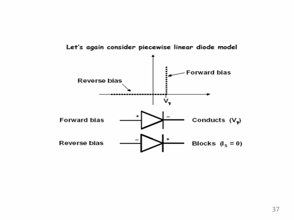
37
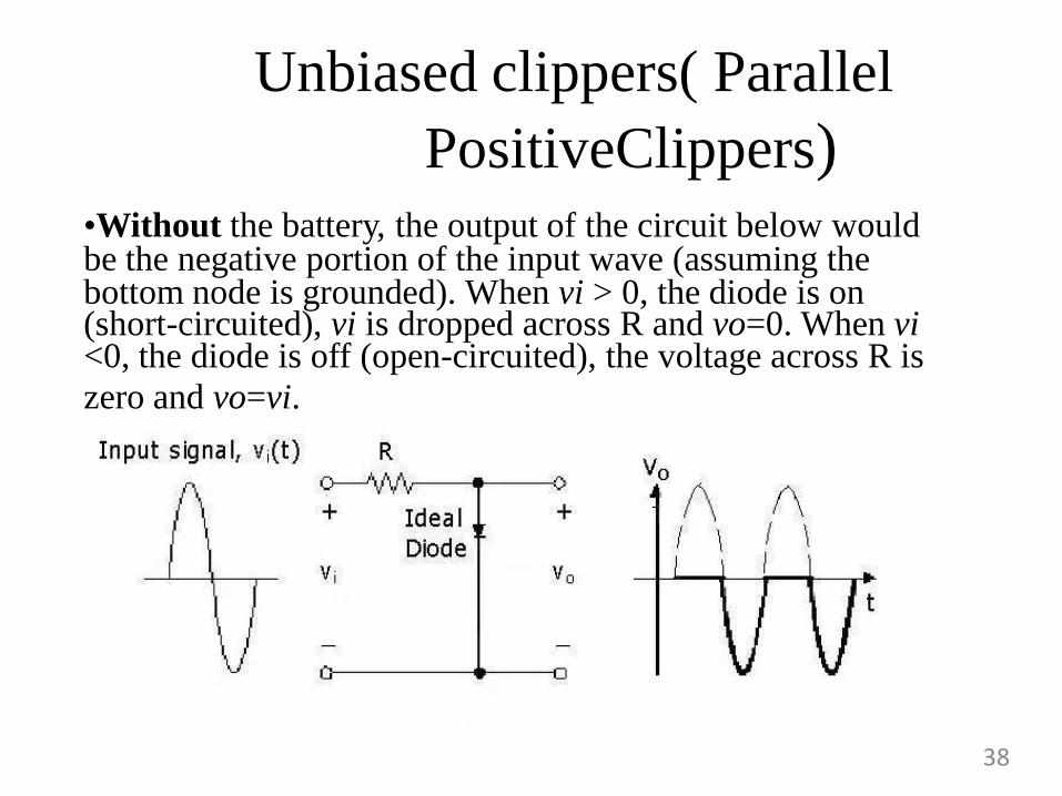
Unbiased clippers( Parallel
PositiveClippers)•Without the battery, the output of the circuit below would be the negative portion of the input wave (assuming thebottom node is grounded). When vi > 0, the diode is on (short-circuited), vi is dropped across R and vo=0. When vi<0, the diode is off (open-circuited), the voltage across R is
zero and vo=vi.
38

Unbiased clippers( Parallel Negative
Clippers)+ive cycle :- anode is at ground potential and cathode sees
variable +ive voltage from 0 to +Vm So complete cycle, the diode is reverse biased and Vo =Vin.At positive peak Vo=+5V
-ive cycle :- anode is at ground potential and cathode sees variable -ive vols from 0 to –Vm. When magnitude of in put volatge i.e / Vin/ >Vd, the diode become forward biased and hence Vo =-Vd =0.7V
39

peaVo=k,-Vm+ Vd =
Series positive clipper
+ive cycle :- anode is at ground potential and cathode sees variable +ive voltage from 0 to +Vm.For comlpete, cycle, diode become reverse biased and hence Vo =0V
-ive cycle :- anode is at ground potential and cathode sees variable -ive voltage from 0 to –Vm. So in complete cycle, the diode is forward biased and Vo= Vin + Vd andAt negative
40

Series Negative clipper
+ive cycle :- anode is at positive potential from 0 to +Vm.Forcomlpete, cycle, diode become forward biased and hence vo= 5v
-ive cycle :- Cathode is at ground potential and cathode sees variable -ive voltage from 0 to –Vm. So in complete cycle, the diode is Reversebiased and negative peak, Vo= 0
41
42
Input
Output
Vγ Vγ
Slope=1 Vi
Vi
Input
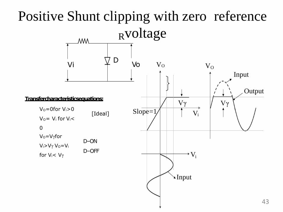
Positive Shunt clipping with zero reference
Rvoltage
Vi
Transfercharacteristicsequations:
DVo VO
VO=0for Vi>0
VO= Vi for Vi<
0
VO=Vγfor
Vi>Vγ VO=Vi
for Vi< Vγ
[Ideal]
D–ON
D–OFF
VO
43

Input
VR + Vγ VR+ VγOutput
Vi
Positive Shunt clipping with positive reference vRoltage
VO VO
Transfer characteristics
equations:
Vi < VR+Vγ D – OFF
VO = Vi
Vi > VR+Vγ
VO = VR+Vγ
D – ON
D
Vi VoVR
44
Vi VRVo
VO VO
Input
Vi
Vi
Output
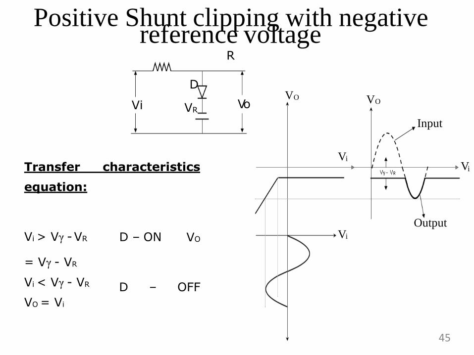
Positive Shunt clipping with negativereference voltage
R
D
ViTransfer characteristics
equation:
Vi > Vγ -VR D – ON VO
= Vγ - VR
Vi < Vγ - VR
VO = Vi
D – OFF
45
Input
-Vγ -Vγ
Vi
Vi
Output
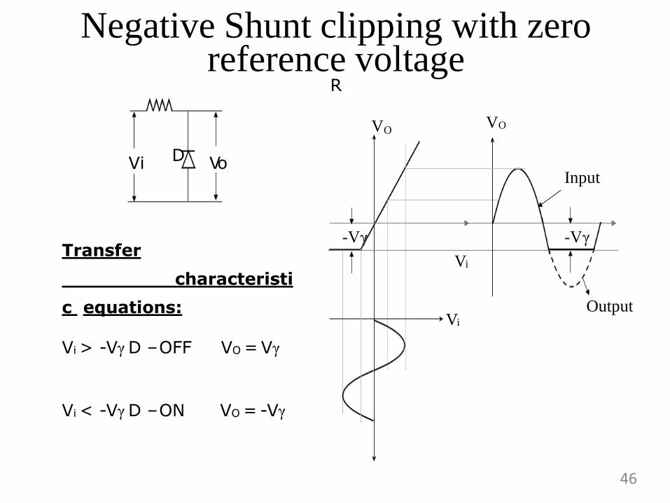
Negative Shunt clipping with zero reference voltage
R
VOVO
Transfer
characteristi
c equations:
Vi > -Vγ D –OFF VO = Vγ
Vi < -Vγ D –ON VO = -Vγ
Vi D Vo
46

Vi
D
VRVo
Negative Shunt clipping with positive reference voltage
R
VO
Transfer characteristics
equations:
VO
DOFF
DON
VR - Vγ Vi
Vi < VR-
Vγ VO = VR-Vγ
D –ON Vi
Vi > VR-Vγ D – OFF
VO = Vi
47
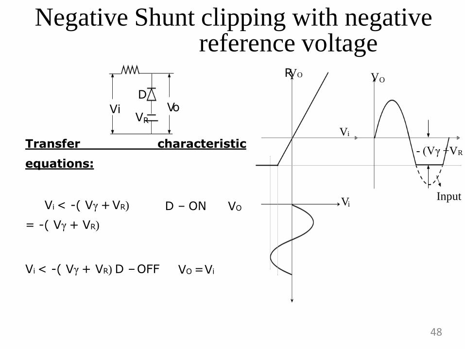
Negative Shunt clipping with negative reference voltage
RVO VO
D
ViVR
Vi
Transfer characteristic
equations:- (Vγ +VR
Vi < -( Vγ +VR)
= -( Vγ + VR)
D – ON VOVi
Input
Vi < -( Vγ + VR) D –OFF VO =Vi
Vo
48

Output
Vi
Vi
D
Negative Series clipper with zeroreference
VOVO
Transfercharacteristicequations:
Vi<0 D–OFF VO=0
Vi>0 D–ON VO=Vi
Vi<Vγ D–OFF VO=0
Vi>Vγ D–ON VO=Vi-Vγ
IdealDiode
PracticalDiode
Vi R Vo
49

V
CLIPPING ATTWO INDEPENDENT LEVELSR
Vi
Transfercharacteristicequations:
D
VR
D
VRVo
VO VO
ViVR
1
Input
Output
i
Inp
ut (Vi) DiodeState
Outp
ut (VO)
Vi VR
1
D1 –ON,D2 – OFF VO =VR
1
VR Vi VR
1 2
D1 –OFF,D2 – OFF VO =Vi
Vi VR2D1 –OFF,D2 – ON VO=VR
2
50
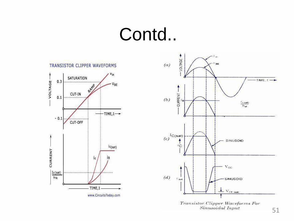
Contd..
51

waveform will be clipped o
Transistor Clipper circuit• The transistor has two types of linearities—One linearity happens when the transistor passes from cut-in region to theactive region. The other linearity occurs when the transistor passes from the
active region to the saturation region. When any input signalpasses through the transistor, across the boundary between cut-in region
and active region, or across the boundary between the active region and saturation region, a portion of the input signal ff.
52

CLAMPING CIRCUIT
•The need to establish the extremity of the positive (or) negative signal excursion at some reference level.When the signal is passedthrough a capacitive coupling network such a signal has lost itsd.c. component. The clamping circuit introduces the d.c.components at the outside, for this reason the coupling circuits arereferred to as d.c. restore (or) d.c. reinserter.
•Def : “ A clamping circuit is one that takes an input waveform and
provides an output i.e., a faithful replica of its shape, but has oneedge clamped to the zero voltage reference point.
There are two types of clamping circuits.
•1)
Negative clamping circuit.
•2)
Positive clamping circuit.
53

Diode :- ClamperPositive Clamper
The circuit for a positive clamper
is shown in the figure. During
the negative half cycle of the
input signal, the diode conducts
and acts like a short circuit. The
output voltage Vo
0 volts . The capacitor is
charged to the peak value of
input voltage Vm. and it behaves
like a battery. During the positive
half of the input signal, the diode
does not conduct and
acts as an open circuit. Hence the
output voltage VoVm+ Vm This
gives a positively clamped
voltage. Vo Vm+ Vm = 2 Vm 54

55

Negative ClamperDuring the positive half
cycle the diode conducts and
acts like a short circuit. The
capacitor charges to peak
value of input voltage Vm.
During this interval
output Vo which is
across the short circuit
the
taken
willbe zero During the negative
half cycle, the diode is open.
The output voltage can be
found by applying KVL.
56
57

Biased Clamper
58
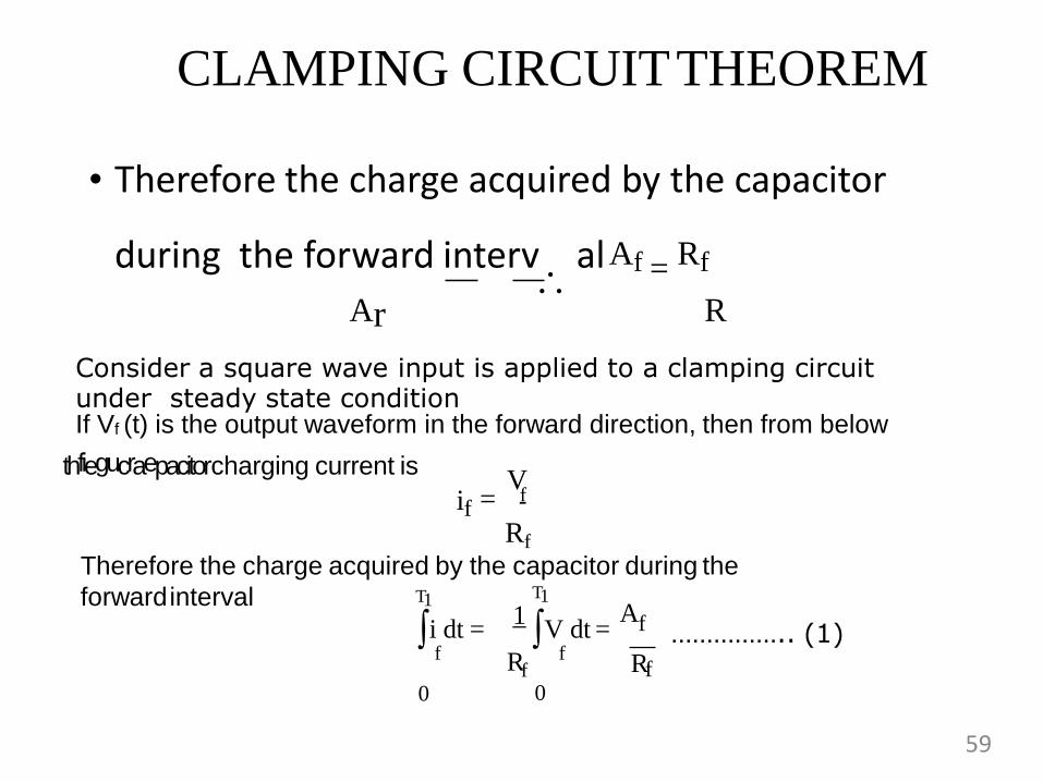
CLAMPING CIRCUITTHEOREM
• Therefore the charge acquired by the capacitor
during the forward interv
alAf = Rf
Ar R
Consider a square wave input is applied to a clamping circuit under steady state conditionIf Vf (t) is the output waveform in the forward direction, then from below
thfiegucraepacitor charging current isV
if = f
Rf
Therefore the charge acquired by the capacitor during the
forwardinterval T1
i dt =
T1
1V dt =
Af …………….. (1)f fRf Rf
0 0
59

• Similarly if Vf (t) is the output voltage in the reverse direction, then the current which discharges by the capacitor is
T2 T2
1
ir dt = R Vrdt=
A
r …………….. (2)
T1 T2 RIn the steady-state the net charge acquired by the capacitor
must be zero.
Therefore from equation (1) & (2) this equation says that for any
input waveform the ratio of the area under the output voltage curve
in the forward direction to the reverse direction is equal to the ratio
.
60

Clamping Circuit taking Source and Diode Resistances into account
61
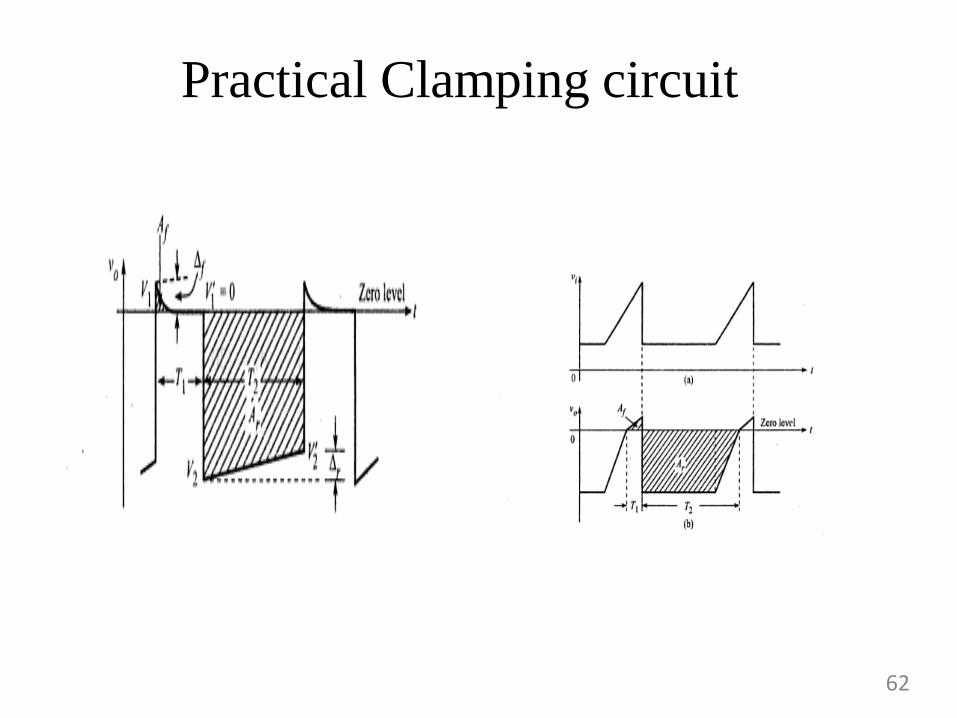
Practical Clamping circuit
62

Effect of diode characteristics on clamping
voltage
63

Synchronized Clamping
64

UNIT-2
MULTIVIBRATORS
65

Multivibrators
• Multivibrator – A circuit designed to have zero, one, or two stable output states.
• There are three types of multivibrators.• Astable (or Free-Running Multivibrator)
• Monostable (or One-Shot)
• Bistable (or Flip-Flop)
66
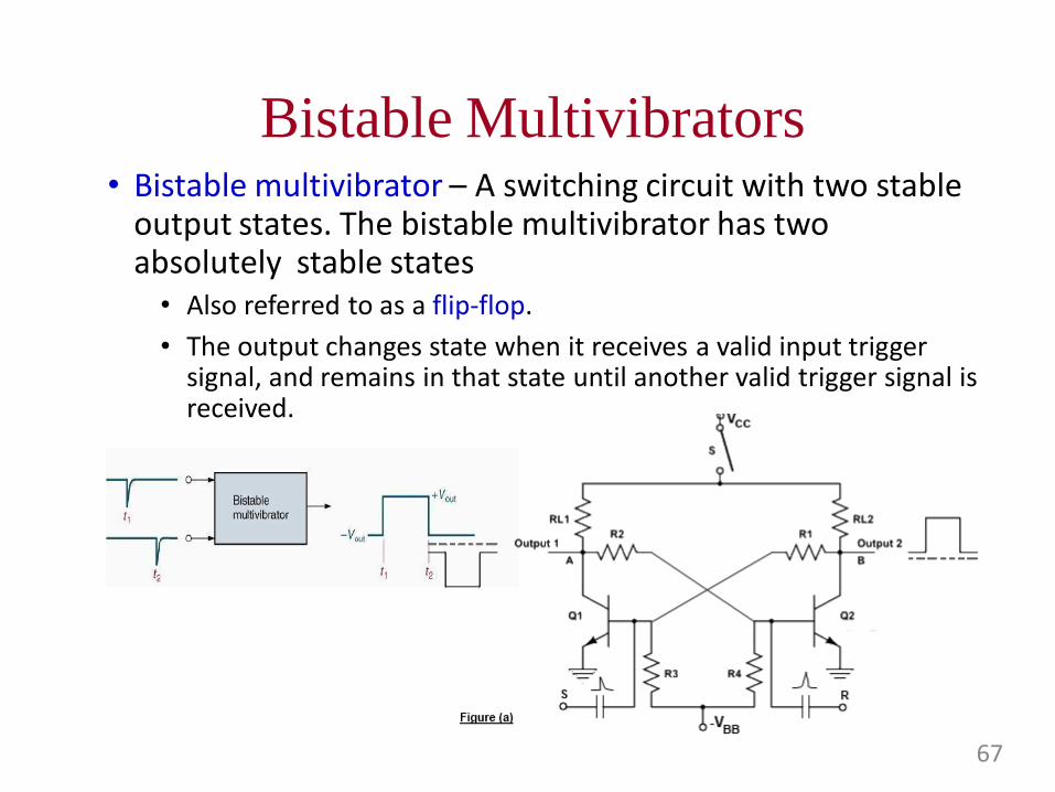
Bistable Multivibrators• Bistable multivibrator – A switching circuit with two stable
output states. The bistable multivibrator has two absolutely stable states
• Also referred to as a flip-flop.
• The output changes state when it receives a valid input trigger signal, and remains in that state until another valid trigger signal is received.
67

Bistable Multivibrator Waveform
68
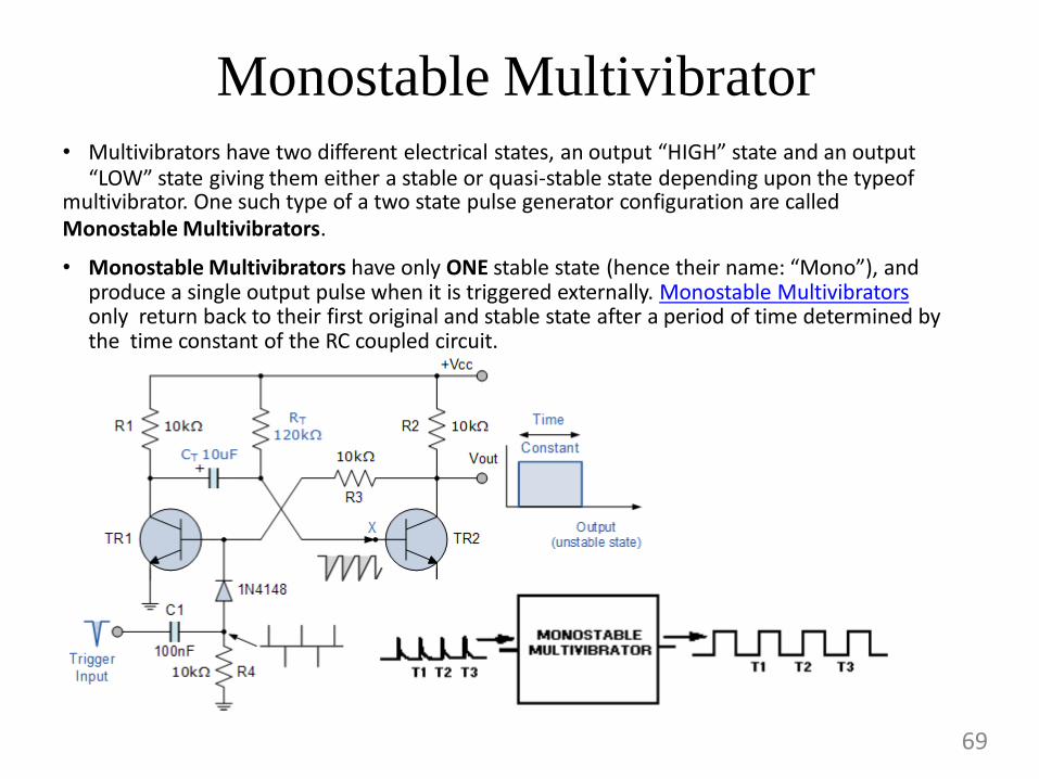
Monostable Multivibrator• Multivibrators have two different electrical states, an output “HIGH” state and an output
“LOW” state giving them either a stable or quasi-stable state depending upon the typeofmultivibrator. One such type of a two state pulse generator configuration are calledMonostable Multivibrators.
• Monostable Multivibrators have only ONE stable state (hence their name: “Mono”), and produce a single output pulse when it is triggered externally. Monostable Multivibratorsonly return back to their first original and stable state after a period of time determined by the time constant of the RC coupled circuit.
69
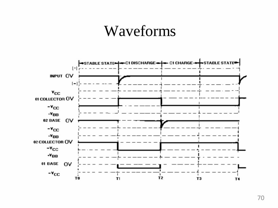
Waveforms
70

Astable Multivibrator
71

Waveforms
72

Commutating Capacitors
• Conduction
transfers takes two
phases
• 1) Transitiontime
• 2) Settling time
73
Triggering the binary
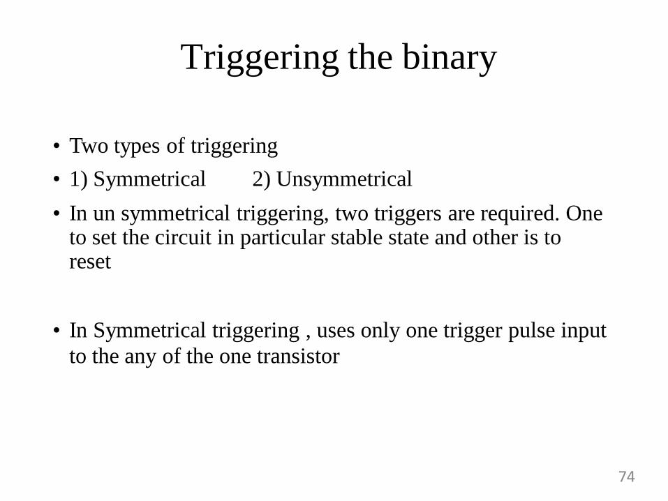
• Two types of triggering
• 1) Symmetrical 2) Unsymmetrical
• In un symmetrical triggering, two triggers are required. One to set the circuit in particular stable state and other is to reset
• In Symmetrical triggering , uses only one trigger pulse input
to the any of the one transistor
74
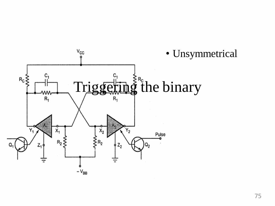
• Unsymmetrical
Triggering the binary
75

symmet
• symmetrical
rical
76

Schmitt Triggers
• Schmitt trigger – A voltage-level detector.
• The output of a Schmitt trigger changes statewhen
• When a positive-going input passes the upper trigger point(UTP) voltage.
• When a negative-going input passes the lower trigger point (LTP) voltage.
77
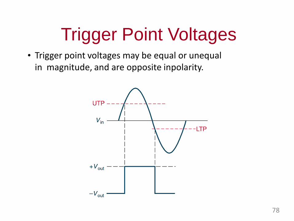
Trigger Point Voltages• Trigger point voltages may be equal or unequal
in magnitude, and are opposite inpolarity.
78
Hysteresis
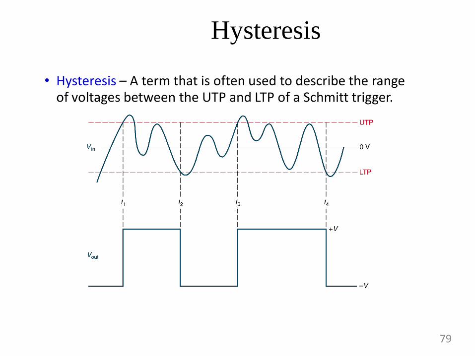
• Hysteresis – A term that is often used to describe the range of voltages between the UTP and LTP of a Schmitt trigger.
79

Schmitt trigger using transister
80

Astable multivibrator to generate a square wave of 1 kHz:
• Assume NPN transistor withh fe 25
• Let Ic5mA
Vcc 12V
T1T2T/2
• Assume symmetrical square wave i.e.
• Neglect the junctionvoltages.
• We have f= 1kHz
• So, T=1/1kHz =1ms
vardhaman 81
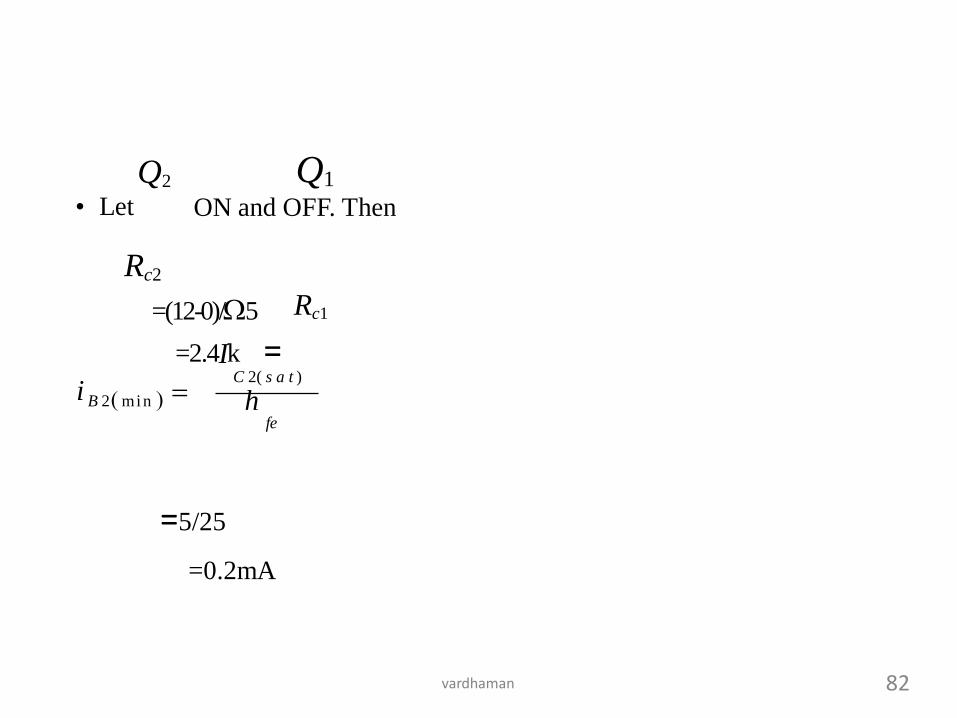
Q2
• Let
Q1
ON and OFF. Then
Rc2
=(12-0)/5 Rc1
=2.4Ik =i B 2mi n
C 2( s a t )
hfe
=5/25
=0.2mA
vardhaman 82

Q2
• When is insaturatio n :
=1.5X0.2
=0.3mA
vardhaman 83
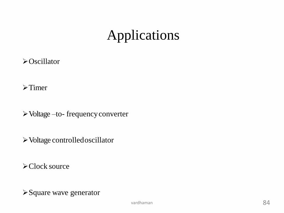
Applications
Oscillator
Timer
Voltage –to- frequencyconverter
Voltage controlledoscillator
Clock source
Square wave generator
vardhaman 84
UNIT - 3
SAMPLING GATES
AND
TIME BASE
GENERATORS
85
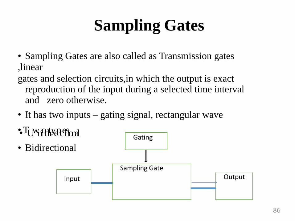
Sampling Gates
• Sampling Gates are also called as Transmission gates,linear
gates and selection circuits,in which the output is exact reproduction of the input during a selected time interval and zero otherwise.
• It has two inputs – gating signal, rectangular wave
••TUwnioditryepcetsional
• Bidirectional
Sampling GateOutputInput
Gating
86
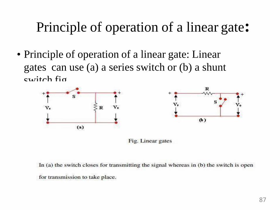
Principle of operation of a linear gate:
• Principle of operation of a linear gate: Linear
gates can use (a) a series switch or (b) a shunt
switch fig
87

Unidirectional Gate
• unidirectional sampling gates are those which transmit signals of only
one
polarity(i.e,. either positive or negative)
• The gating signal is also known as control pulse, selector pulse or an enabling pulse. It is a negative signal, the magnitude of which changes abruptly between –V2 and –V1.
88
Unidirectional gate
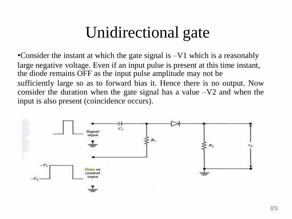
•Consider the instant at which the gate signal is –V1 which is a reasonably
large negative voltage. Even if an input pulse is present at this time instant,the diode remains OFF as the input pulse amplitude may not be
sufficiently large so as to forward bias it. Hence there is no output. Nowconsider the duration when the gate signal has a value –V2 and when theinput is also present (coincidence occurs).
89
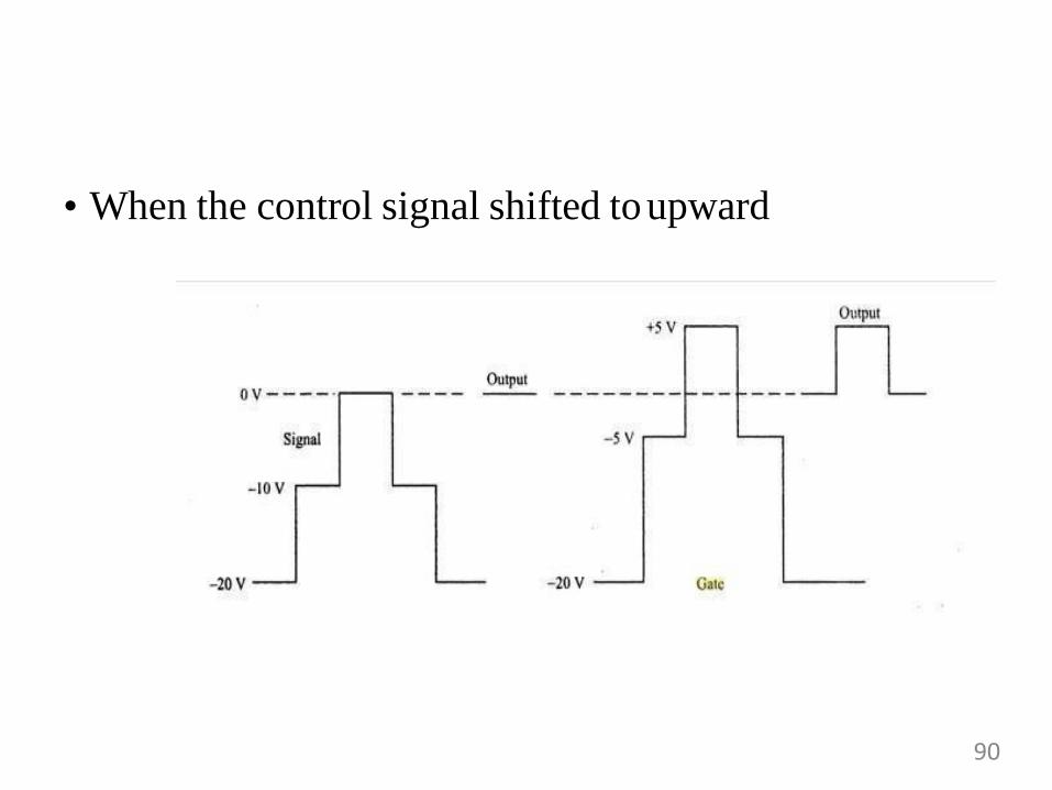
Output waveform
• When the control signal shifted toupward
90
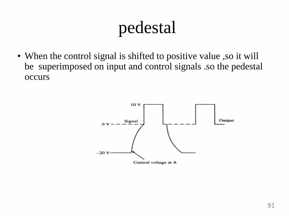
pedestal
• When the control signal is shifted to positive value ,so it will be superimposed on input and control signals .so the pedestal occurs
91

Unidirectional diode coincidence gate•When any of the control
voltages is at –V1, point X is ata large negative voltage, evenif the input pulse Vs is present., D0 is reverse biased. Hence there is no signal at the output.
•When all the control voltages, on the other hand, are at –V2 , if an input signal Vs is present, D0 is forward biased and the output is a pulse of 5V. Hence this circuit is a coincidence circuit or AND circuit.
92
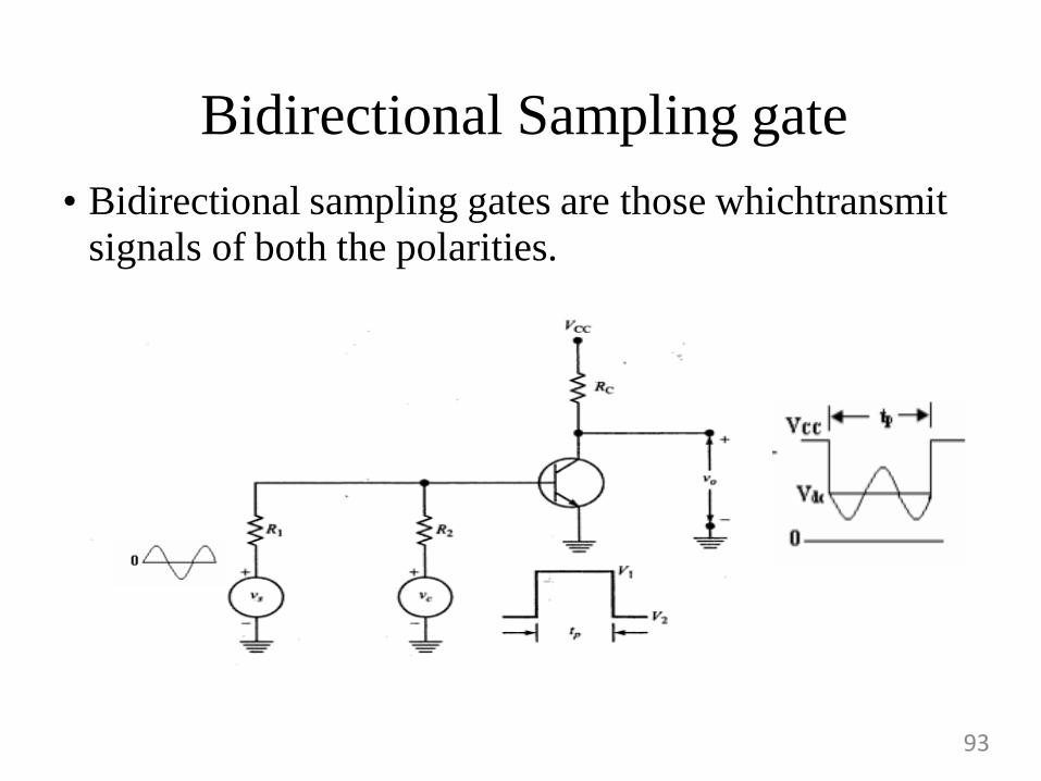
Bidirectional Sampling gate
• Bidirectional sampling gates are those whichtransmit
signals of both the polarities.
93

Bidirectional Sampling gate
using Transistor• Bidirectionalsampling gates are those which transmitsignals of both thepolarities.
94
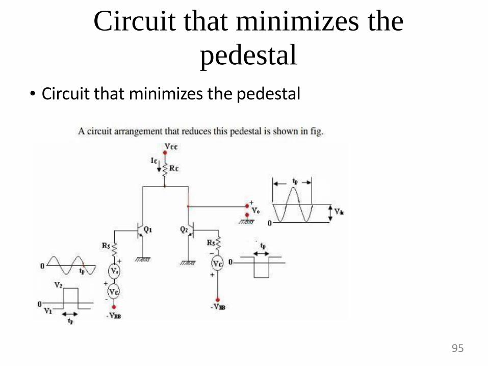
Circuit that minimizes the
pedestal
• Circuit that minimizes the pedestal
95
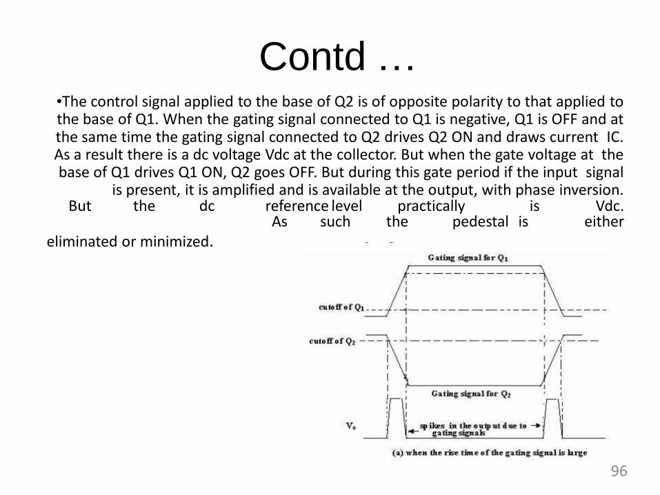
Contd …•The control signal applied to the base of Q2 is of opposite polarity to that applied to the base of Q1. When the gating signal connected to Q1 is negative, Q1 is OFF and at the same time the gating signal connected to Q2 drives Q2 ON and draws current IC. As a result there is a dc voltage Vdc at the collector. But when the gate voltage at the base of Q1 drives Q1 ON, Q2 goes OFF. But during this gate period if the input signal
is present, it is amplified and is available at the output, with phase inversion.But the dc reference level practically is Vdc.
As such the pedestal is eithereliminated or minimized.
96

Two Diode Sampling gate•When the control signals are at V1, D1 and D2 are OFF, no input signal is transmitted to the output. But when control signals are at V2, diode D1conducts if the input is positive pulses and diode D2 conducts if the input is negative pulses. Hence these bidirectional inputs are transmitted to the output. This arrangement eliminates pedestal, because of the circuit symmetry.
97

Four Diode Sampling gate• When the control signals are at V1, D1 and D2 are OFF, no inputsignal is transmitted to the output. But when control signals are atV2, diode D1 conducts if the input is positive pulses and diode D2conducts if the input is negative pulses. Hence these bidirectionalinputs are transmitted to the output. This
arrangement eliminates pedestal, because of the circuit symmetry.
98

Applications
• ChopperAmplifier
• Multiplexers
• ADC
• Sampling Scope
• Sample and hold circuits
99
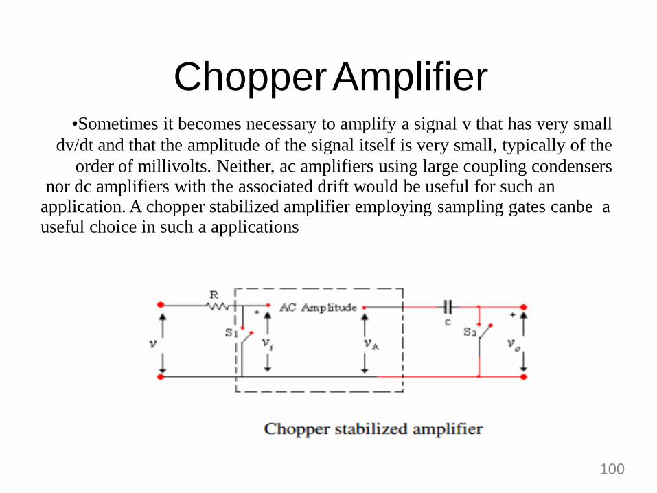
ChopperAmplifier•Sometimes it becomes necessary to amplify a signal v that has very small
dv/dt and that the amplitude of the signal itself is very small, typically of the
order of millivolts. Neither, ac amplifiers using large coupling condensersnor dc amplifiers with the associated drift would be useful for such an
application. A chopper stabilized amplifier employing sampling gates canbe a useful choice in such a applications
100

General features of time base
generator
101
Time base generator Constant current charging
A capacitor is charged with constant current source.
As it charged with constant current, it is charged linearly.
Miller circuit:
Integrator is used to convert a step waveform to ramp waveform.
Bootstrap circuits
A constant current source is obtained by maintaining nearly constant voltage across the fixed resistor in series with capacitor.
Compensating network is used to improve the linearity of bootstrap andmiller time base generator
102

Exponential sweep circuit
103
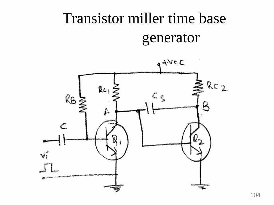
Transistor miller time base
generator
104

Input and output waveforms
105
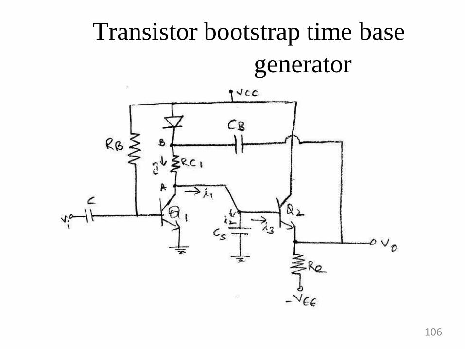
Transistor bootstrap time base
generator
106

Input and output waveforms
107
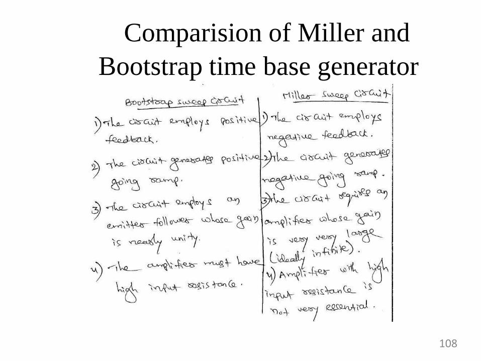
Comparision of Miller and
Bootstrap time base generator
108
UNIT-4
SYNCHRONIZATION
AND
FREQUENCY
DIVISION
109
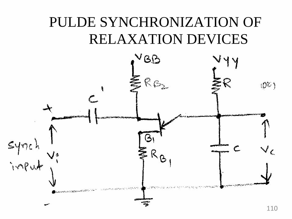
PULDE SYNCHRONIZATION OF
RELAXATION DEVICES
110
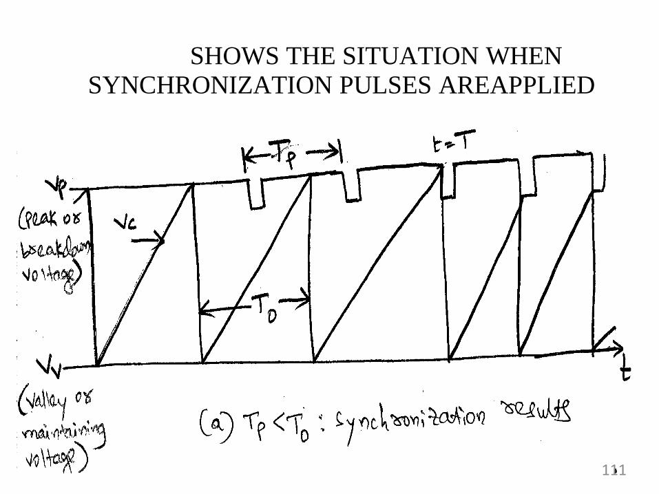
SHOWS THE SITUATION WHEN
SYNCHRONIZATION PULSES AREAPPLIED
111

SHOWS THE CASE WHEN TP>TO
112

FREQUENCYDIVISION
113

ASTABLE RELAXATION CIRCUIT
114

WAVEFORMS WHEN POSITIVE
PULSES ARE APPLIED
TOB1
115
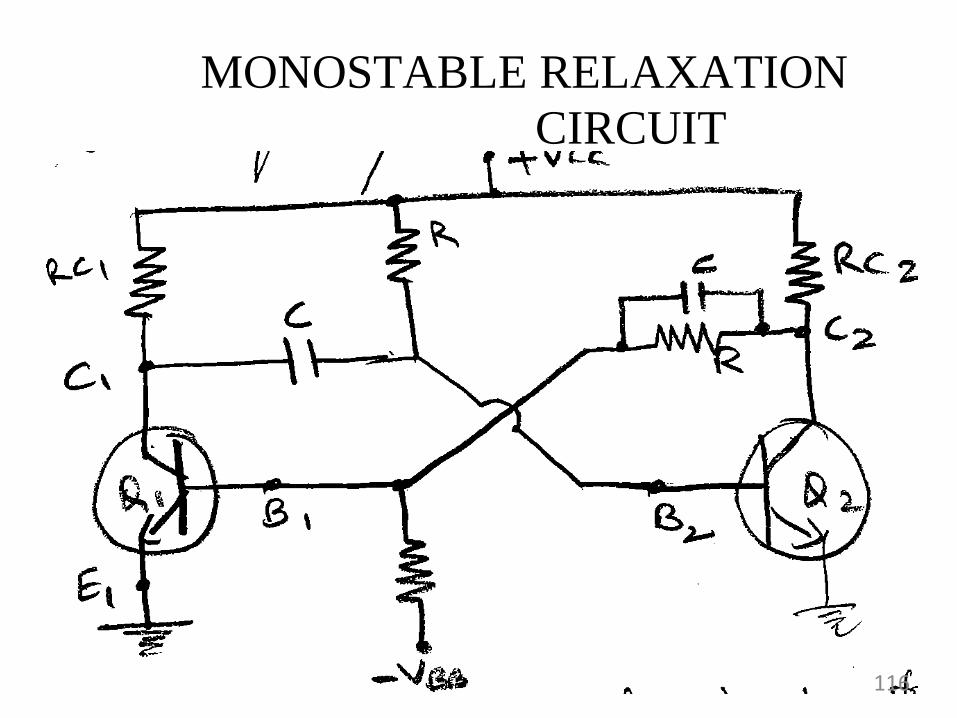
MONOSTABLE RELAXATION
CIRCUIT
116

WAVEFORM AT B2 WITH NO PULSE OVERSHOOT AND WITH
PULSE OVERSHOOT
117

METHOD FOR ACHIEVING DIVISION WITH PHASE JITTER
118
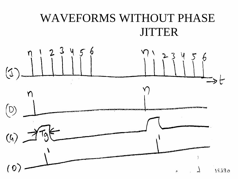
WAVEFORMS WITHOUT PHASE
JITTER
119

SYNCHRONIZATION WITH
SINE WAVE
120

FREQUENCY DIVISION WITH
SYNC SIGNAL
121

UNIT-5
DIGITAL LOGIC FAMILIES
122
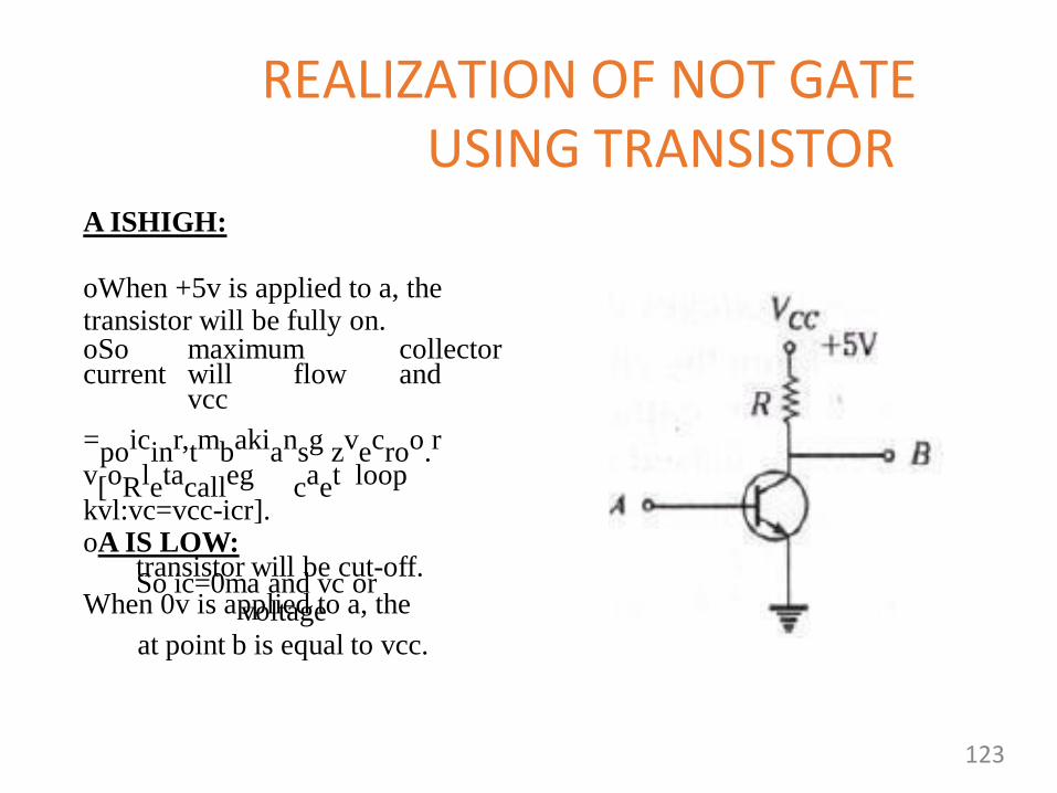
REALIZATION OF NOT GATE USING TRANSISTOR
A ISHIGH:
oWhen +5v is applied to a, the transistor will be fully on.oSo maximum collector current will flow and
vcc
=poicinr,tmbakiansg zvecroo.r
v[oRletacalleg caet loop
kvl:vc=vcc-icr].oA IS LOW:
When 0v is applied to a, the
transistor will be cut-off.So ic=0ma and vc or
voltage
at point b is equal to vcc.
123

TTL (Transistor Transistor Logic) Integrated-circuit technology that
uses the bipolar transistor as the principal circuit element.
CMOS (Complimentary Metal Oxide Semiconductor) Integrated-circuit
technology that uses the field-effect transistor as the principal circuit element.
ECL (Emitter Coupled Logic) Integrated-circuit technology that uses the bipolar
transistors configured as a differential amplifier. This eliminates saturation and
improves speed but uses more power than other families.
124

OTHER DIGITAL IC SPECIFICATIONS
• Drive Capabilities- sometimes referred to as fan-in or fan-
out.
• Fan out- number of inputs of a logic family that can be driven by a single output. The drive capability of outputs.
• Fan in- the load an input places on an output.
• Propagation delay- has to do with the “speed” of the logicelement. Lower propagation delays mean higher speedwhich is a desirable characteristic.
• Power Dissipation- generally, as propagation delaysdecrease, power consumption and heat generation
increase.
CMOS is noted for low power consumption.
125
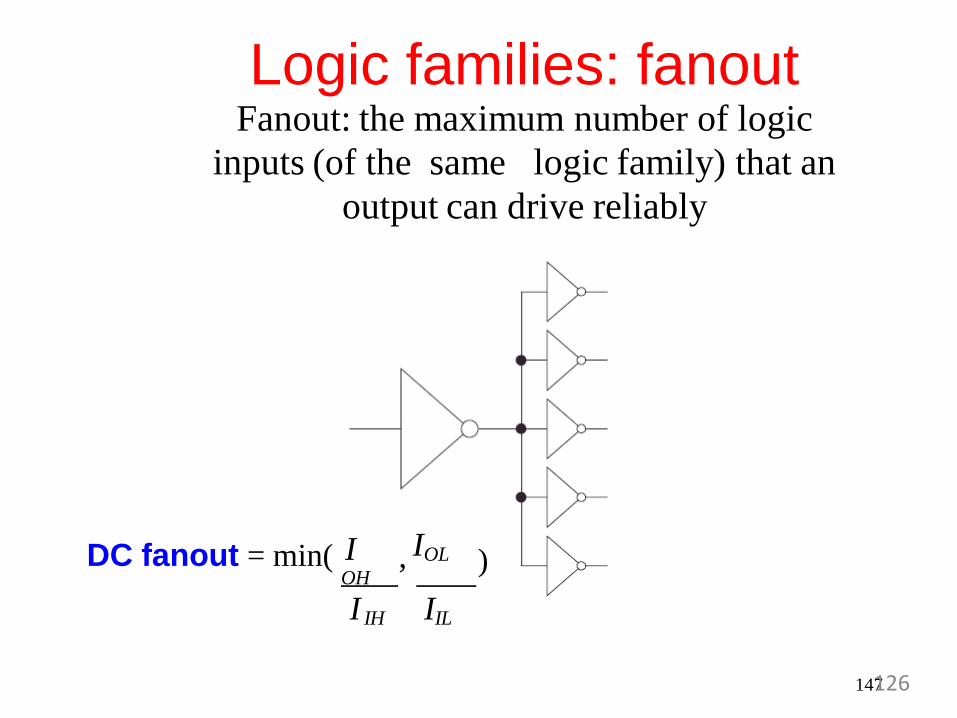
Logic families: fanoutFanout: the maximum number of logic
inputs (of the same logic family) that an
output can drive reliably
DC fanout = min( I , IOL )OH
I IH IIL
147126
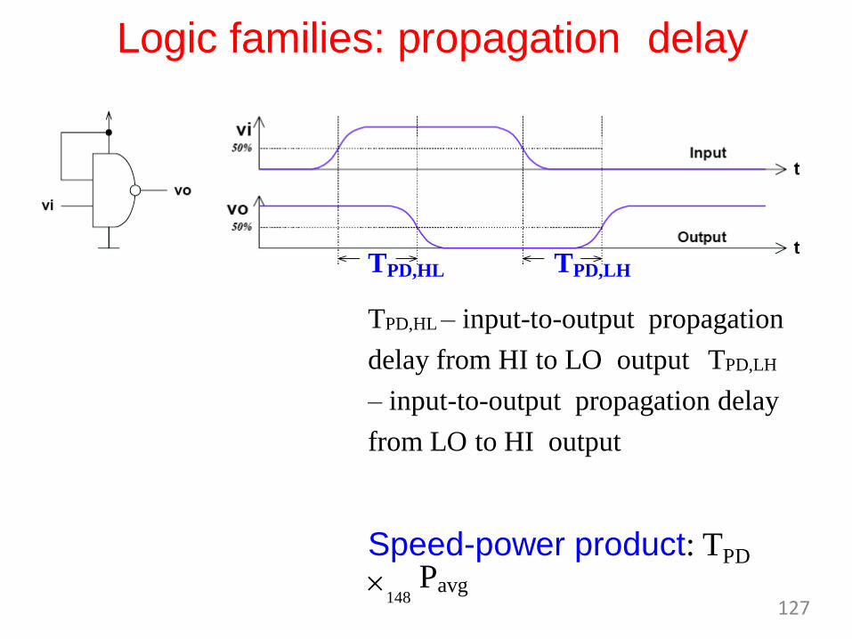
Logic families: propagation delay
TPD,HL TPD,LH
TPD,HL – input-to-output propagation
delay from HI to LO output TPD,LH
– input-to-output propagation delay
from LO to HI output
Speed-power product: TPD
148
Pavg127

Logic families: noise marginHI state noisemargin:
VNH = VOH(min) – VIH(min)
LO state noise margin:
VNL = VIL(max) – VOL(max)
Noise margin:
VN = min(VNH,VNL)
149
VNH
VNL
128

TOTEM POLE NAND GATE
• First introduced by in 1964 (Texas Instruments)
• TTL has shaped digital technology in many ways
• Standard TTL family
(e.g. 7400) is
obsolete
• Newer TTL families still
used (e.g.
74ALS00)129
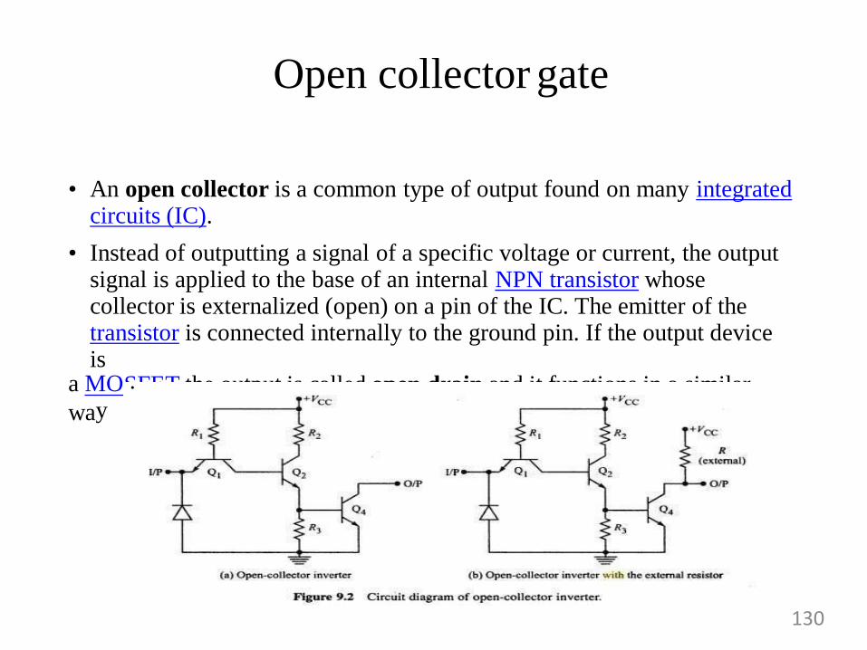
SFET the output is called open drain and it functions in a similar
Open collector gate
• An open collector is a common type of output found on many integrated circuits (IC).
• Instead of outputting a signal of a specific voltage or current, the output signal is applied to the base of an internal NPN transistor whose collector is externalized (open) on a pin of the IC. The emitter of the transistor is connected internally to the ground pin. If the output device is
a MO .
way
130

TristateTTL
• Tristate means a state of logic other than „1‟ and
„0‟ in which there is a high impedance state and there is no isource or isink at the output stage transistor (or MOSFET). A gate capable of being in „1‟, „0‟ and ntrai statteristateis
131

Direct-coupled transistor logic (DCTL)
• Direct-coupled transistor logic (DCTL) is similar to resistor–transistor logic (RTL) but the input transistor bases are connecteddirectly to the collector outputs without any base resistors.Consequently, DCTL gates have fewer components, are moreeconomical, and are simpler to fabricate onto integrated circuitsthan RTL gates. Unfortunately, DCTL has much smaller signal levels, has more susceptibility to ground noise, and requiresmatched transistor characteristics. The transistors are also heavilyoverdriven; that is a good feature in that it reduces the saturationvoltage of the output transistors, but it also slows the circuit down due to a high stored charge in the base.[1] Gate fan-out is limiteddue to "current hogging": if the transistor base-emitter voltages(VB)E are not well matched, then the base-emitter junction of onetransistor may conduct most of the input drive current at such a low base-emitter voltage that other input transistors fail to turn on
132

ECL
Emitter-Coupled Logic (ECL)
•PROS: Fastest logic family available (~1ns)
•CONS: low noise margin and high power dissipation
•Operated in emitter coupled geometry (recall
differential amplifier or emitter-follower), transistors
are biased and operate near their Q-point (never near
saturation!)
•Logic levels. “0”: –1.7V. “1”: –0.8V
•Such strange logic levels require extra effort when
interfacing to TTL/CMOS logic families.
•Open LTspice example: ECL inverter…
154133
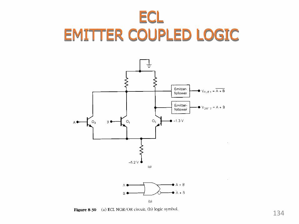
ECLEMITTER COUPLED LOGIC
134
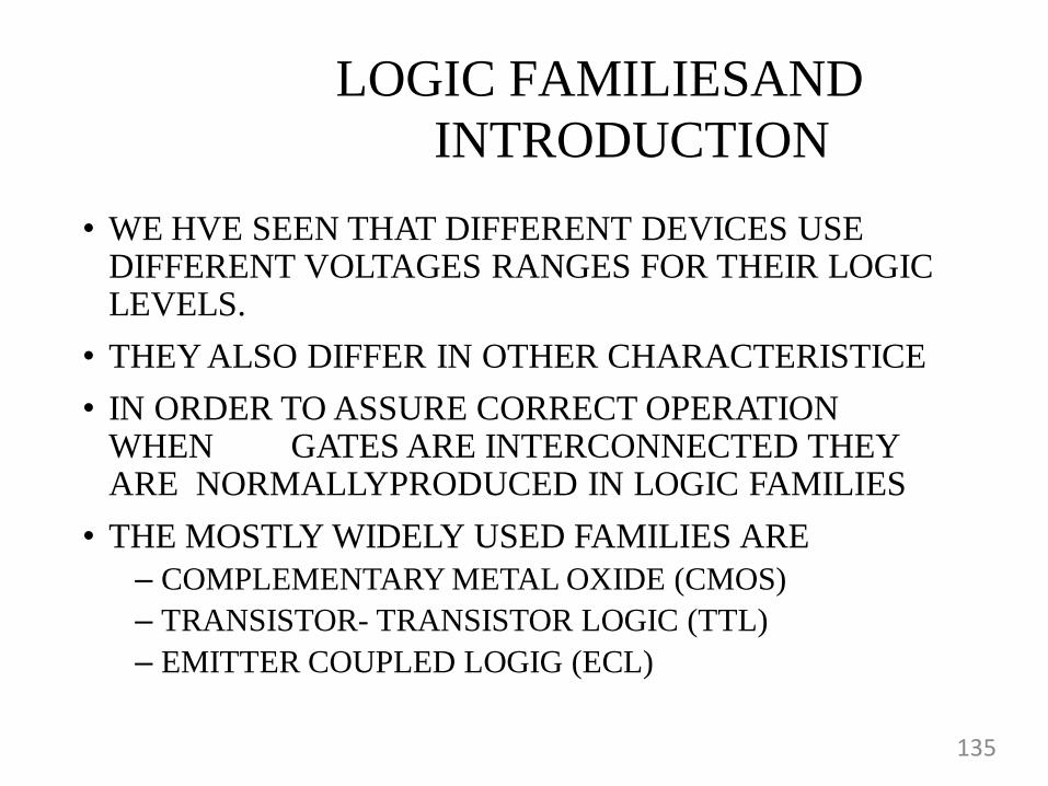
LOGIC FAMILIESAND
INTRODUCTION
• WE HVE SEEN THAT DIFFERENT DEVICES USE DIFFERENT VOLTAGES RANGES FOR THEIR LOGIC LEVELS.
• THEY ALSO DIFFER IN OTHER CHARACTERISTICE
• IN ORDER TO ASSURE CORRECT OPERATION WHEN GATES ARE INTERCONNECTED THEY ARE NORMALLYPRODUCED IN LOGIC FAMILIES
• THE MOSTLY WIDELY USED FAMILIES ARE
– COMPLEMENTARY METAL OXIDE (CMOS)
– TRANSISTOR- TRANSISTOR LOGIC (TTL)
– EMITTER COUPLED LOGIG (ECL)
135
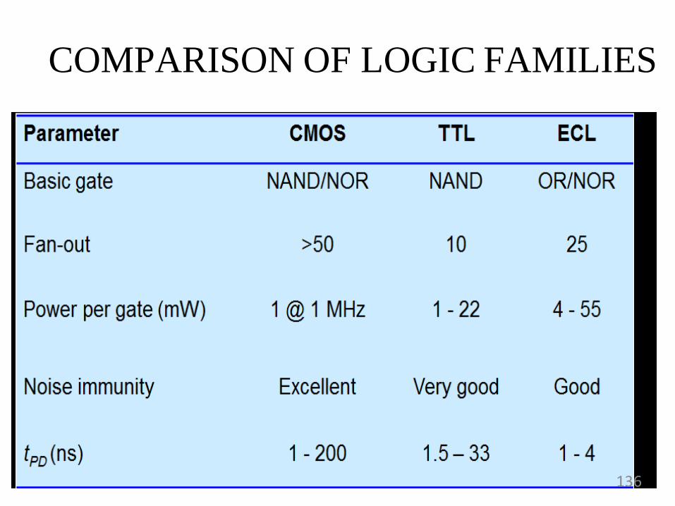
COMPARISON OF LOGIC FAMILIES
136

Thank you
137