Embed Size (px)
Citation preview
PTH Core-to-Core Interconnect Using Sintered Conductive Pastes
Michael Matthews, Ken Holcomb, Jim Haley, and Catherine Shearer
Ormet Circuits, Inc.
10080 Willow Creek Road, San Diego, CA, 92131
P: 858.831.0010, F: 858.831.1437, web: ormetcircuits.com
Abstract
The market for high-layer-count printed circuit boards (PCB) containing blind and buried vias was once relatively small, and
focused on specialized applications in the military and high end computing. The demand for these types of PCBs today is
being driven by an increasing number of commercial applications in the telecommunications and semiconductor test market
segments. These applications typically require high-aspect-ratio plated-through-holes (PTHs) and blind and buried vias in
order to meet the applications interconnect density requirements. Blind and buried vias and high aspect ratio PTHs continue
to present manufacturing challenges and frequently are the limiting features to achieving high fabrication yield. Multiple
lamination cycles, the indeterminate yield of sub-cores, backdrilling and extended plating times add to the overall poor yield
of high layer count PCBs. An attractive solution to the high-aspect-ratio PTH dilemma is to break the high-layer-count PCB
into a number of subassemblies that can be 100% inspected and then be interconnected. Conductive paste-based
interconnects are an attractive interconnect technology option, but passively loaded copper or silver filled pastes do not
demonstrate the requisite performance and reliability. Sintering conductive pastes, which metallurgically bond directly to the
copper pads of the PCB during a standard lamination cycle, do meet the requirements of these high-layer-count PCBs and at
substantially lower cost than conventional manufacturing methods.
Key words:
Sintering conductive paste, telecommunications, connection of subassemblies, high-layer-count PCBs, high throughput and
yield, PCB for semiconductor test, low cost and reliable
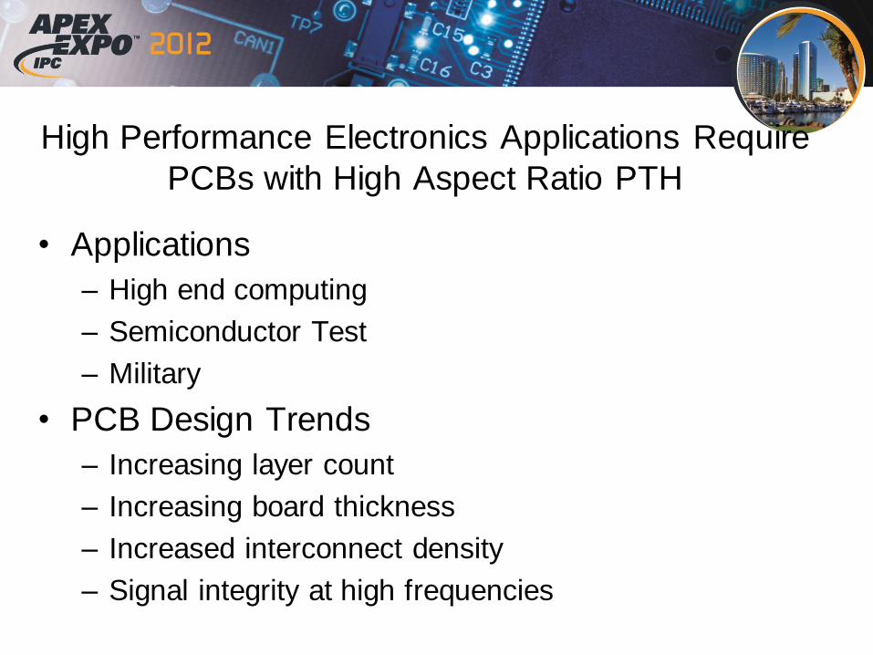
Introduction
The production of high-layer-count PCBs for the telecommunications, semiconductor test and high end computing industries
requires an advanced set of fabrication techniques due to the complexity of their design. Frequently, manufacture of these
PCBs requires the use of blind and buried vias, high-aspect-ratio plated through holes and backdrilling to meet their design
specifications. The technical roadmap for industries utilizing high layer count PCBs indicates that future PCB designs will be
increasingly complex and there is a drive toward higher interconnect density.
The reliability demands on high layer count boards are also increasing due to the increasing power dissipation requirements
and higher operating frequencies of telecom, high end computing and military applications. This increase in thermal exposure
Global PCB Market
Pro
du
ctio
n V
olu
mes
Low
High
PCB Fabrication TechnologyLow High
Consumer Electronics
Digital CamerasFeature Phones
Smart PhonesTablet Computers
Semiconductor Test
Military
High End ComputingTelecomServers
Figure 1. Global PCB Market (High Layer Count Applications in bold)
over the lifespan of the PCB exacerbates the need for robust electrical interconnect structures throughout the board.
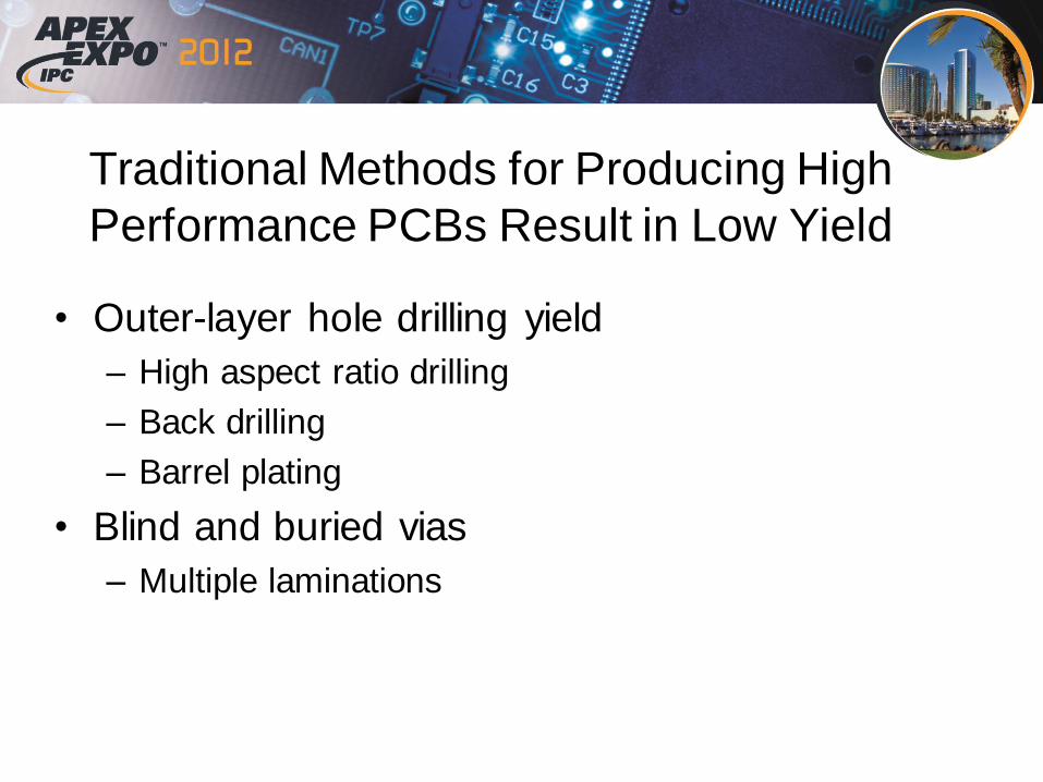
With the widespread adoption of 0.4mm pitch components, and the desire to route multiple circuit traces between copper
pads, fabricators are being pushed to use smaller drill sizes and plate ever higher aspect ratio holes. The fine featured PTHs in
these boards increase the cost of the final board as they are slow to fabricate, as well as expensive and difficult to plate
consistently.
One solution to the difficulty of plating the high-aspect-ratio PTH in these PCBs is to break the PCB into subassemblies or
‘cores’ with manageable-sized PTHs. By breaking the PCB into cores of reasonable thickness, the PTHs of these cores can be
plated in high quality, yield and throughput. These cores may then be interconnected using paste interconnects to form a
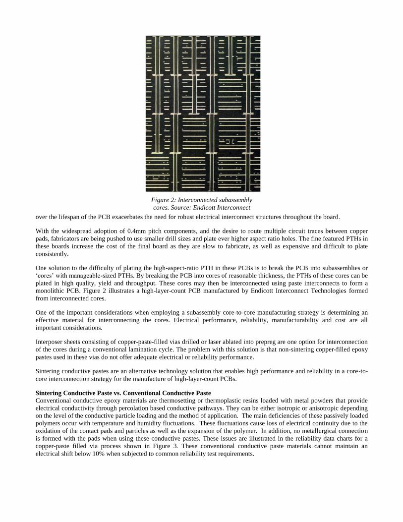
monolithic PCB. Figure 2 illustrates a high-layer-count PCB manufactured by Endicott Interconnect Technologies formed
from interconnected cores.
One of the important considerations when employing a subassembly core-to-core manufacturing strategy is determining an
effective material for interconnecting the cores. Electrical performance, reliability, manufacturability and cost are all
important considerations.
Interposer sheets consisting of copper-paste-filled vias drilled or laser ablated into prepreg are one option for interconnection
of the cores during a conventional lamination cycle. The problem with this solution is that non-sintering copper-filled epoxy
pastes used in these vias do not offer adequate electrical or reliability performance.
Sintering conductive pastes are an alternative technology solution that enables high performance and reliability in a core-to-
core interconnection strategy for the manufacture of high-layer-count PCBs.
Sintering Conductive Paste vs. Conventional Conductive Paste
Conventional conductive epoxy materials are thermosetting or thermoplastic resins loaded with metal powders that provide
electrical conductivity through percolation based conductive pathways. They can be either isotropic or anisotropic depending
on the level of the conductive particle loading and the method of application. The main deficiencies of these passively loaded
polymers occur with temperature and humidity fluctuations. These fluctuations cause loss of electrical continuity due to the
oxidation of the contact pads and particles as well as the expansion of the polymer. In addition, no metallurgical connection
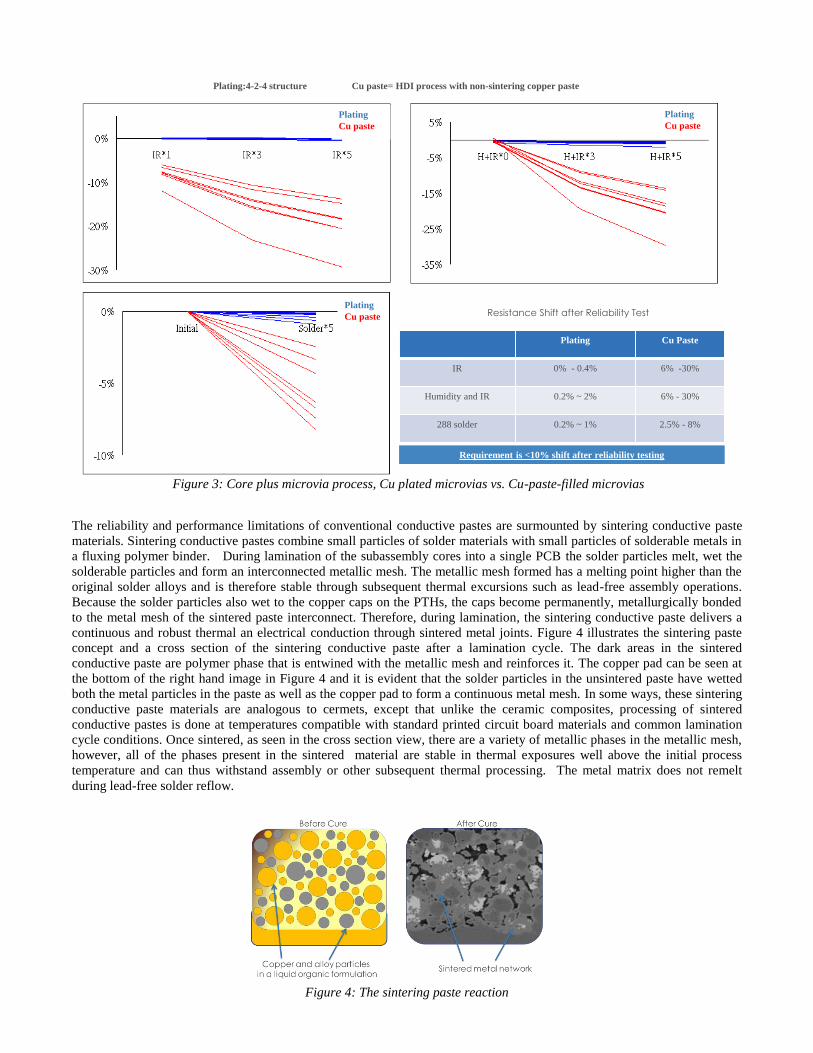
is formed with the pads when using these conductive pastes. These issues are illustrated in the reliability data charts for a
copper-paste filled via process shown in Figure 3. These conventional conductive paste materials cannot maintain an
electrical shift below 10% when subjected to common reliability test requirements.
Figure 2: Interconnected subassembly
cores. Source: Endicott Interconnect
The reliability and performance limitations of conventional conductive pastes are surmounted by sintering conductive paste
materials. Sintering conductive pastes combine small particles of solder materials with small particles of solderable metals in
a fluxing polymer binder. During lamination of the subassembly cores into a single PCB the solder particles melt, wet the
solderable particles and form an interconnected metallic mesh. The metallic mesh formed has a melting point higher than the
original solder alloys and is therefore stable through subsequent thermal excursions such as lead-free assembly operations.
Because the solder particles also wet to the copper caps on the PTHs, the caps become permanently, metallurgically bonded
to the metal mesh of the sintered paste interconnect. Therefore, during lamination, the sintering conductive paste delivers a
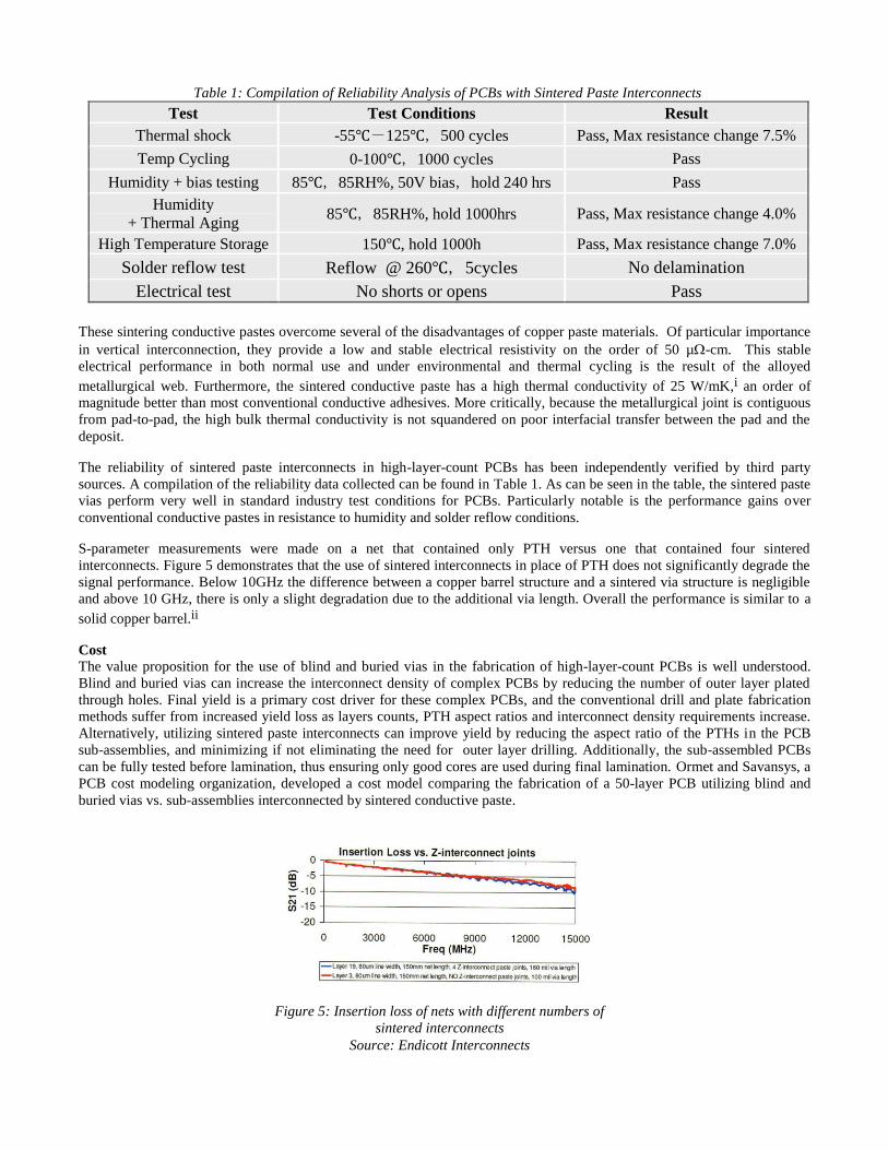
continuous and robust thermal an electrical conduction through sintered metal joints. Figure 4 illustrates the sintering paste
concept and a cross section of the sintering conductive paste after a lamination cycle. The dark areas in the sintered
conductive paste are polymer phase that is entwined with the metallic mesh and reinforces it. The copper pad can be seen at
the bottom of the right hand image in Figure 4 and it is evident that the solder particles in the unsintered paste have wetted
both the metal particles in the paste as well as the copper pad to form a continuous metal mesh. In some ways, these sintering
conductive paste materials are analogous to cermets, except that unlike the ceramic composites, processing of sintered
conductive pastes is done at temperatures compatible with standard printed circuit board materials and common lamination
cycle conditions. Once sintered, as seen in the cross section view, there are a variety of metallic phases in the metallic mesh,
however, all of the phases present in the sintered material are stable in thermal exposures well above the initial process
temperature and can thus withstand assembly or other subsequent thermal processing. The metal matrix does not remelt
during lead-free solder reflow.
Figure 4: The sintering paste reaction
Plating:4-2-4 structure Cu paste= HDI process with non-sintering copper paste
Requirement is <10% shift after reliability testing
Resistance Shift after Reliability Test
Plating
Cu paste
Plating
Cu paste
Plating
Cu paste
Plating Cu Paste
IR 0% - 0.4% 6% -30%
Humidity and IR 0.2% ~ 2% 6% - 30%
288 solder 0.2% ~ 1% 2.5% - 8%
Figure 3: Core plus microvia process, Cu plated microvias vs. Cu-paste-filled microvias
These sintering conductive pastes overcome several of the disadvantages of copper paste materials. Of particular importance
in vertical interconnection, they provide a low and stable electrical resistivity on the order of 50 µ-cm. This stable
electrical performance in both normal use and under environmental and thermal cycling is the result of the alloyed
metallurgical web. Furthermore, the sintered conductive paste has a high thermal conductivity of 25 W/mK,i an order of
magnitude better than most conventional conductive adhesives. More critically, because the metallurgical joint is contiguous
from pad-to-pad, the high bulk thermal conductivity is not squandered on poor interfacial transfer between the pad and the
deposit.
The reliability of sintered paste interconnects in high-layer-count PCBs has been independently verified by third party
sources. A compilation of the reliability data collected can be found in Table 1. As can be seen in the table, the sintered paste
vias perform very well in standard industry test conditions for PCBs. Particularly notable is the performance gains over
conventional conductive pastes in resistance to humidity and solder reflow conditions.
S-parameter measurements were made on a net that contained only PTH versus one that contained four sintered
interconnects. Figure 5 demonstrates that the use of sintered interconnects in place of PTH does not significantly degrade the
signal performance. Below 10GHz the difference between a copper barrel structure and a sintered via structure is negligible
and above 10 GHz, there is only a slight degradation due to the additional via length. Overall the performance is similar to a
solid copper barrel.ii
Cost
The value proposition for the use of blind and buried vias in the fabrication of high-layer-count PCBs is well understood.
Blind and buried vias can increase the interconnect density of complex PCBs by reducing the number of outer layer plated
through holes. Final yield is a primary cost driver for these complex PCBs, and the conventional drill and plate fabrication
methods suffer from increased yield loss as layers counts, PTH aspect ratios and interconnect density requirements increase.
Alternatively, utilizing sintered paste interconnects can improve yield by reducing the aspect ratio of the PTHs in the PCB
sub-assemblies, and minimizing if not eliminating the need for outer layer drilling. Additionally, the sub-assembled PCBs
can be fully tested before lamination, thus ensuring only good cores are used during final lamination. Ormet and Savansys, a
PCB cost modeling organization, developed a cost model comparing the fabrication of a 50-layer PCB utilizing blind and
buried vias vs. sub-assemblies interconnected by sintered conductive paste.
Table 1: Compilation of Reliability Analysis of PCBs with Sintered Paste Interconnects
Test Test Conditions Result
Thermal shock -55℃-125℃,500 cycles Pass, Max resistance change 7.5%
Temp Cycling 0-100℃,1000 cycles Pass
Humidity + bias testing 85℃,85RH%, 50V bias,hold 240 hrs Pass
Humidity
+ Thermal Aging 85℃,85RH%, hold 1000hrs Pass, Max resistance change 4.0%
High Temperature Storage 150℃, hold 1000h Pass, Max resistance change 7.0%
Solder reflow test Reflow @ 260℃,5cycles No delamination
Electrical test No shorts or opens Pass
Figure 5: Insertion loss of nets with different numbers of
sintered interconnects
Source: Endicott Interconnects
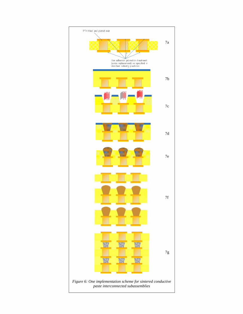
Figure 6: One implementation scheme for sintered conductive
paste interconnected subassemblies
7a
7b
7c
7d
7e
7f
7g
The output of the model is summarized in Figure 6. The results of the model indicate that by using a sintered paste
interconnect strategy, there can be substantial costs savings versus conventional processes. The savings is driven by
eliminating the need for low yielding drill processes to connect the outer PCB layer, and that sintered paste interconnects
enable the full electrical testing of each of the cores prior to lamination.
Implementation of Sintered Paste Interconnections
There are a variety of ways in which sintering paste interconnections can be implemented in core-to-core integration for high-
layer-count PCBs. The specific method of manufacture will depend on the equipment, process flow and general practices of
any one manufacturing facility. Flexibility of process flow is one of the advantages of paste interconnect technology. Because
the sintering conductive paste interconnects during standard pre-preg lamination conditions, the number of subassemblies, the
method of application of the sintering paste, the manufacturing flow and the specific configuration are all at the discretion of
the manufacturer.
A generalized concept of how the sintered interconnections might be installed is depicted in Figure 6 (a-g). Subassembly
cores are manufactured using standard PTH manufacturing methods. The number of subassemblies created for each PCB is at
the discretion of the manufacturer. The PTHs are filled and cap plated to form a land for the sintered paste interconnects (a).
Generally an adhesion promotion treatment is applied to the outer surfaces of the cores to ensure good bonding with the
prepreg during lamination of the cores, as is standard industry practice for laminated PCB. Prepreg and a release sheet,
generally PET film, are tack laminated to one side of the mating pairs of cores (b). The prepreg may consist of one or more
layers depending on the thickness of the copper on the surface. Via holes are laser ablated through the PET film and prepreg
using the copper cap plate as a stop for the laser (c). Alternatively the vias could be performed by punching, or mechanically
drilling prior to attachment of the prepreg to the core. Sintering conductive paste is then deposited into the vias using the PET
film as a mask (d). The PET film is removed (e). The subassemblies bearing the interconnect layers are aligned (f) and
laminated under standard lamination conditions. When the board is removed from the lamination press, all of the electrical
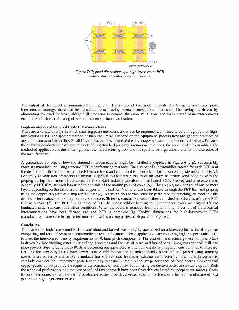
interconnections have been formed and the PCB is complete (g). Typical dimensions for high-layer-count PCBs
manufactured using core-to-core interconnection with sintering pastes are depicted in Figure 7.
Conclusion
The market for high-layer-count PCBs using blind and buried vias is highly specialized on addressing the needs of high end
computing, military, telecom and semiconductor test applications. These applications are requiring higher aspect ratio PTHs
to meet the interconnect density requirements for 0.4mm pitch components. The cost of manufacturing these complex PCBs
is driven by low yielding outer layer drilling processes and the use of blind and buried vias. Using conventional drill and
plate process steps to build these PCBs is becoming unsupportable as interconnect density requirements continue to increase.
Creating the necessary PCBs from several subassemblies that can be independently fabricated and joined using sintering
pastes is an attractive alternative manufacturing strategy that leverages existing manufacturing flow. It is important to
carefully consider the interconnect paste technology to ensure suitable reliability performance of these boards. Conventional
copper pastes do not provide the requisite performance or reliability, but sintering conductive pastes are a viable option. Both
the technical performance and the cost benefit of this approach have been favorably evaluated by independent sources. Core-
to-core interconnection with sintering conductive pastes provides a vetted solution for the cost-effective manufacture of next
generation high layer count PCBs.
Figure 7: Typical dimensions of a high-layer-count PCB
interconnected with sintered paste vias

References
i R. E. Taylor, H. Groot, and J. Ferrier, TPRL Report 1584, “Thermophysical Properties of Conductive Ink.”
ii Das, Rabindra, Egitto, Frank, Lauffer, John, Antesberger, Tim and Markovich, Voya, “Z-Axis Interconnections for Next
Generation Packaging,” Advancing Microelectronics, Vol. 38 No. 6, pp 12-19
PTH Core-to-Core Interconnect
Using Sintered Conductive Pastes
Jim Haley, Ken Holcomb,
Michael Matthews, and Catherine Shearer
Ormet Circuits, Inc.
10080 Willow Creek Road, San Diego, CA, 92131
p: 858.831.0010, f:858.831.1437, web: ormetcircuits.com
High Performance Electronics Applications Require
PCBs with High Aspect Ratio PTH
• Applications
– High end computing
– Semiconductor Test
– Military
• PCB Design Trends
– Increasing layer count
– Increasing board thickness
– Increased interconnect density
– Signal integrity at high frequencies
Traditional Methods for Producing High
Performance PCBs Result in Low Yield
• Outer-layer hole drilling yield
– High aspect ratio drilling
– Back drilling
– Barrel plating
• Blind and buried vias
– Multiple laminations
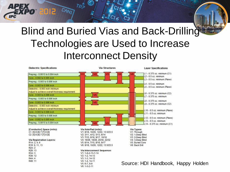
Blind and Buried Vias and Back-Drilling
Technologies are Used to Increase
Interconnect Density
Source: HDI Handbook, Happy Holden
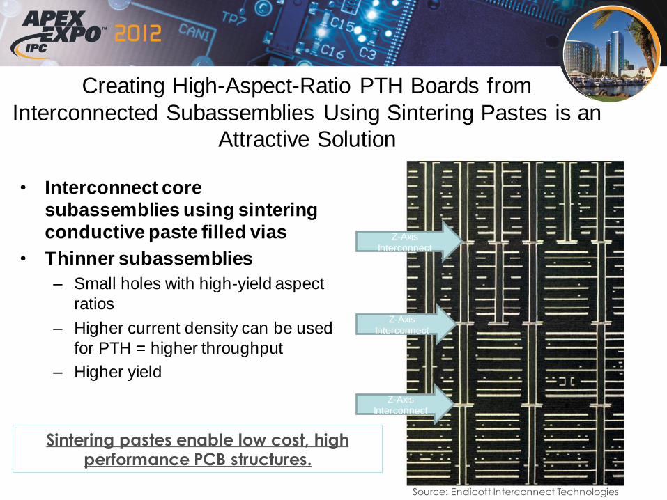
Creating High-Aspect-Ratio PTH Boards from
Interconnected Subassemblies Using Sintering Pastes is an
Attractive Solution
• Interconnect core
subassemblies using sintering
conductive paste filled vias
• Thinner subassemblies
– Small holes with high-yield aspect
ratios
– Higher current density can be used
for PTH = higher throughput
– Higher yield
Z-Axis Interconnect
Z-Axis Interconnect
Z-Axis Interconnect
Source: Endicott Interconnect Technologies
Sintering pastes enable low cost, high performance PCB structures.
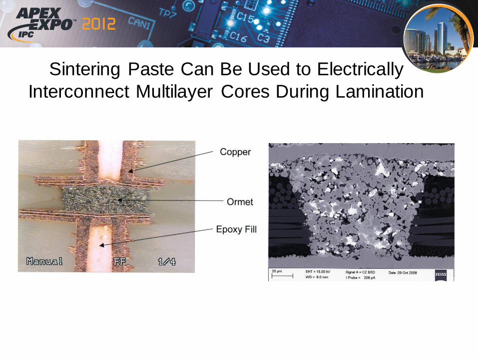
Sintering Paste Can Be Used to Electrically
Interconnect Multilayer Cores During Lamination
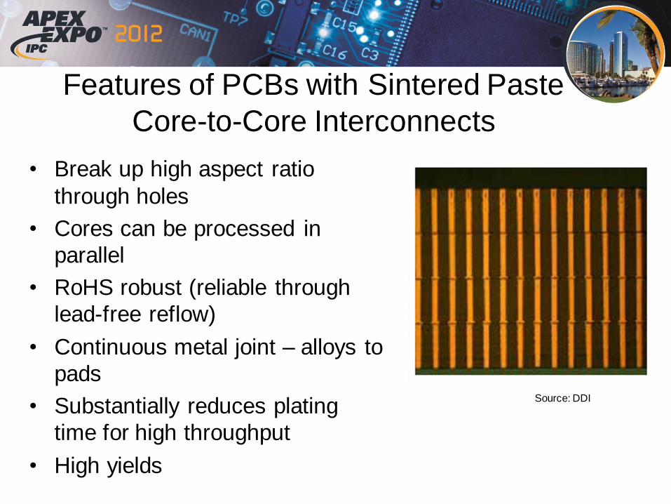
Features of PCBs with Sintered Paste
Core-to-Core Interconnects
• Break up high aspect ratio
through holes
• Cores can be processed in
parallel
• RoHS robust (reliable through
lead-free reflow)
• Continuous metal joint – alloys to
pads
• Substantially reduces plating
time for high throughput
• High yields
Source: DDI
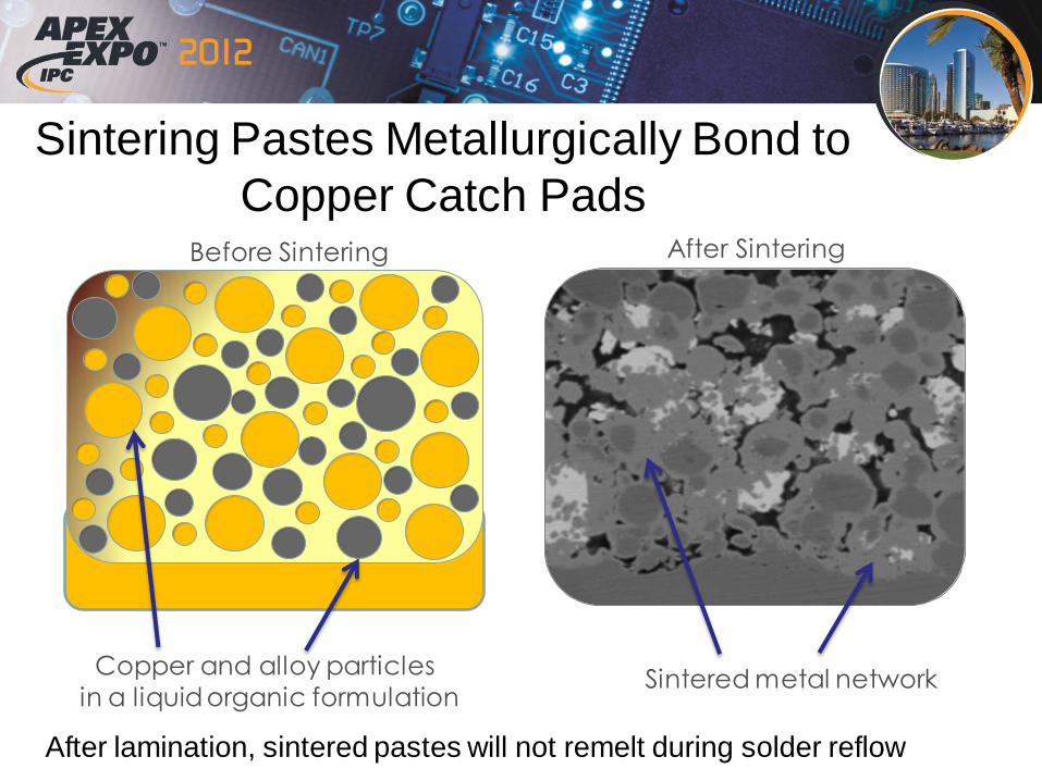
Sintering Pastes Metallurgically Bond to
Copper Catch Pads
Sintered metal network Copper and alloy particles
in a liquid organic formulation
Before Sintering After Sintering
After lamination, sintered pastes will not remelt during solder reflow
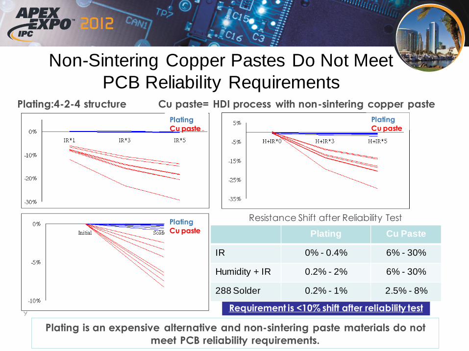
Non-Sintering Copper Pastes Do Not Meet
PCB Reliability Requirements
288 solder dip
IR reflows Humidity + IR
9
Plating is an expensive alternative and non-sintering paste materials do not
meet PCB reliability requirements.
Plating:4-2-4 structure Cu paste= HDI process with non-sintering copper paste
Requirement is <10% shift after reliability test
Resistance Shift after Reliability Test
Plating
Cu paste
Plating
Cu paste
Plating Cu paste
Plating Cu Paste
IR 0% - 0.4% 6% - 30%
Humidity + IR 0.2% - 2% 6% - 30%
288 Solder 0.2% - 1% 2.5% - 8%
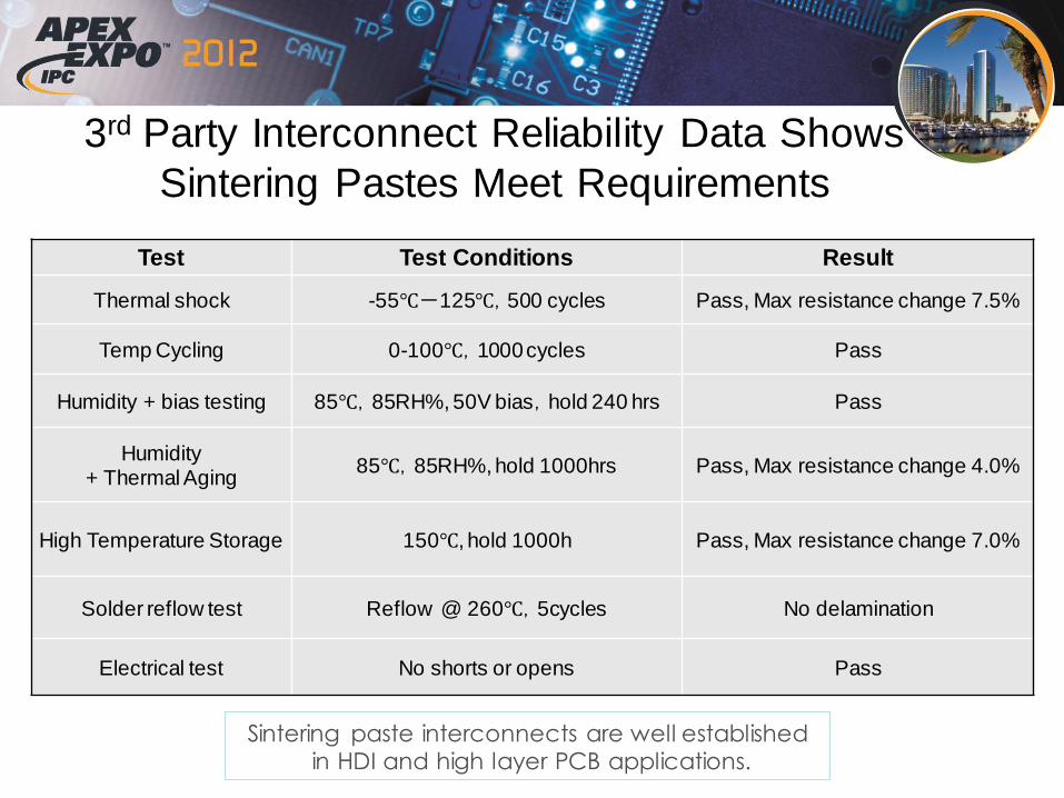
3rd Party Interconnect Reliability Data Shows
Sintering Pastes Meet Requirements
Test Test Conditions Result
Thermal shock -55℃-125℃,500 cycles Pass, Max resistance change 7.5%
Temp Cycling 0-100℃,1000 cycles Pass
Humidity + bias testing 85℃,85RH%, 50V bias,hold 240 hrs Pass
Humidity + Thermal Aging
85℃,85RH%, hold 1000hrs Pass, Max resistance change 4.0%
High Temperature Storage 150℃, hold 1000h Pass, Max resistance change 7.0%
Solder reflow test Reflow @ 260℃,5cycles No delamination
Electrical test No shorts or opens Pass
Sintering paste interconnects are well established in HDI and high layer PCB applications.
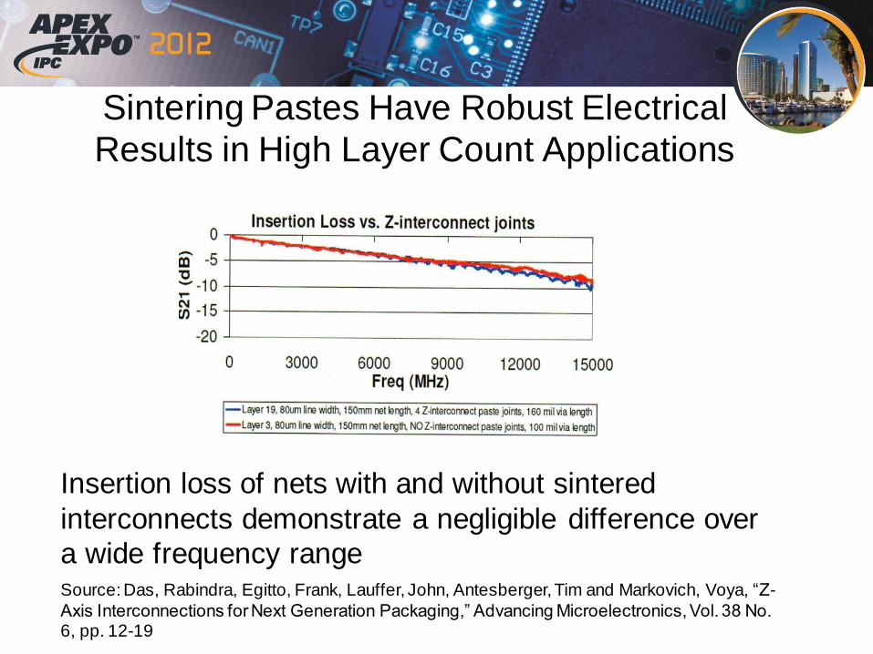
Sintering Pastes Have Robust Electrical
Results in High Layer Count Applications
Insertion loss of nets with and without sintered
interconnects demonstrate a negligible difference over
a wide frequency range Source: Das, Rabindra, Egitto, Frank, Lauffer, John, Antesberger, Tim and Markovich, Voya, “Z-
Axis Interconnections for Next Generation Packaging,” Advancing Microelectronics, Vol. 38 No. 6, pp. 12-19
Sintered Paste Interconnects can Lower
Costs of High Layer Count PCBs
• Cost Savings
– Elimination of outer-layer drilling
– Higher yield from reduced aspect ratio plating
– Higher yield from known good cores
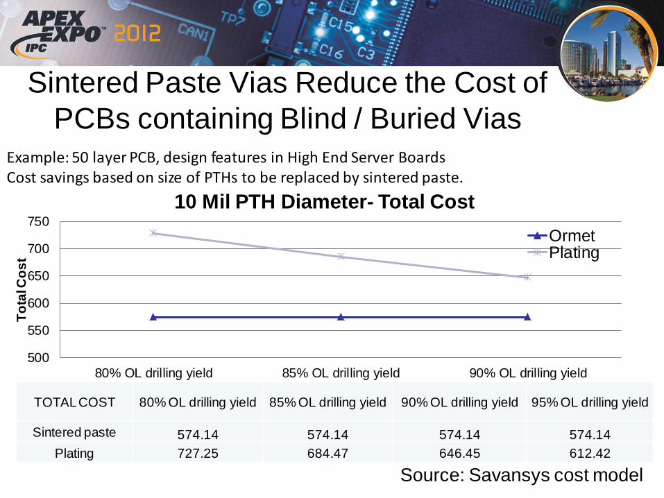
Sintered Paste Vias Reduce the Cost of
PCBs containing Blind / Buried Vias Example: 50 layer PCB, design features in High End Server Boards Cost savings based on size of PTHs to be replaced by sintered paste.
TOTAL COST 80% OL drilling yield 85% OL drilling yield 90% OL drilling yield 95% OL drilling yield
Sintered paste 574.14 574.14 574.14 574.14
Plating 727.25 684.47 646.45 612.42
500
550
600
650
700
750
80% OL drilling yield 85% OL drilling yield 90% OL drilling yield
To
tal C
os
t
10 Mil PTH Diameter- Total Cost
OrmetPlating
Source: Savansys cost model
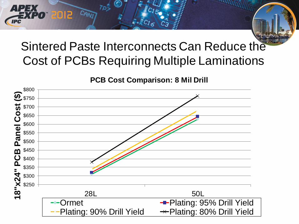
Sintered Paste Interconnects Can Reduce the
Cost of PCBs Requiring Multiple Laminations
$250
$300
$350
$400
$450
$500
$550
$600
$650
$700
$750
$800
28L 50L18"x24" P
CB
Pan
el C
ost ($
)
PCB Cost Comparison: 8 Mil Drill
Ormet Plating: 95% Drill YieldPlating: 90% Drill Yield Plating: 80% Drill Yield
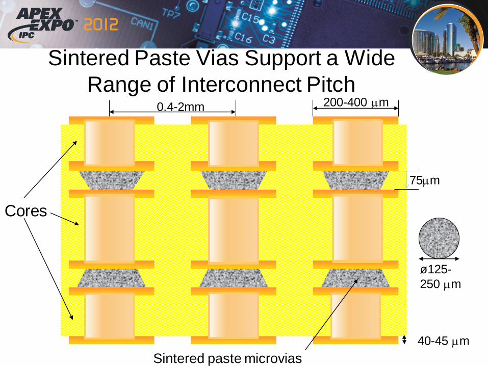
Sintered Paste Vias Support a Wide
Range of Interconnect Pitch
Sintered paste microvias
200-400 m 0.4-2mm
ø125-
250 m
75m
40-45 m
Cores
Implementing Paste Interconnects can be
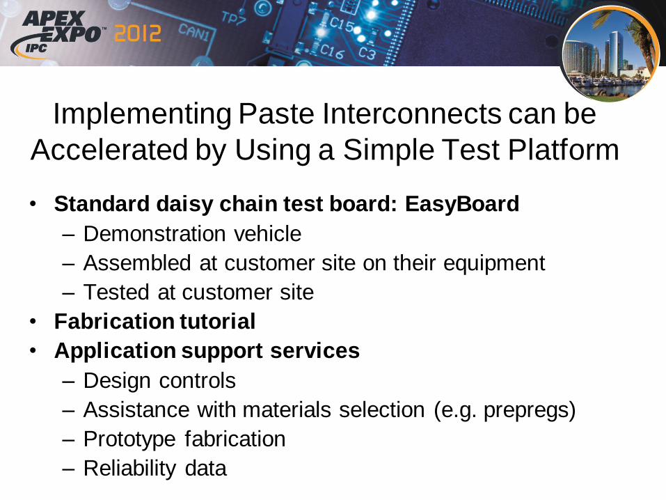
Accelerated by Using a Simple Test Platform
• Standard daisy chain test board: EasyBoard
– Demonstration vehicle
– Assembled at customer site on their equipment
– Tested at customer site
• Fabrication tutorial
• Application support services
– Design controls
– Assistance with materials selection (e.g. prepregs)
– Prototype fabrication
– Reliability data
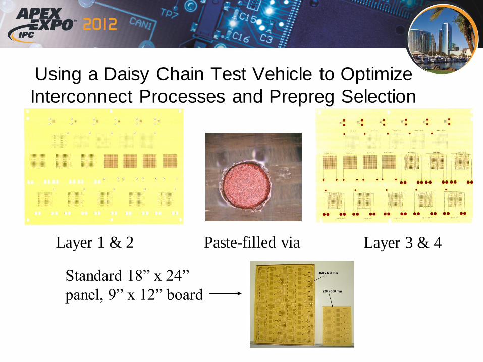
Using a Daisy Chain Test Vehicle to Optimize
Interconnect Processes and Prepreg Selection
Layer 1 & 2 Paste-filled via Layer 3 & 4
Standard 18” x 24”
panel, 9” x 12” board
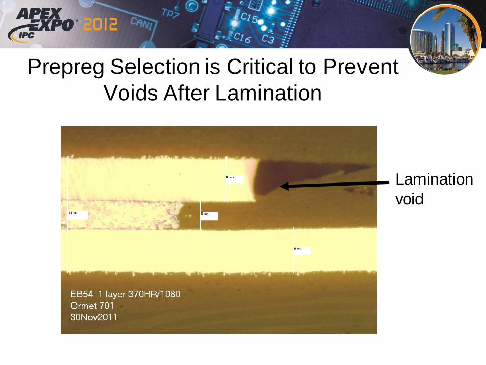
Prepreg Selection is Critical to Prevent
Voids After Lamination
Lamination
void
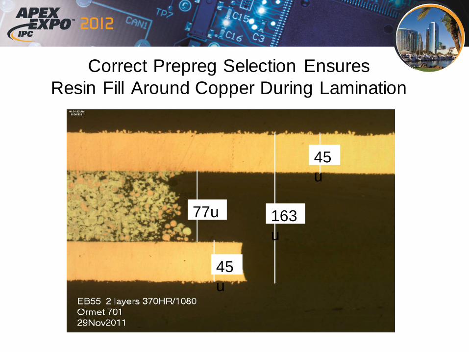
Correct Prepreg Selection Ensures
Resin Fill Around Copper During Lamination
45
u
45
u
77u 163
u

Laser Drilling of Prepregs is a Critical
Process to Ensure Robust Paste
Interconnection
Laser ablation of prepreg requires very different
parameters than forming vias in cured laminate
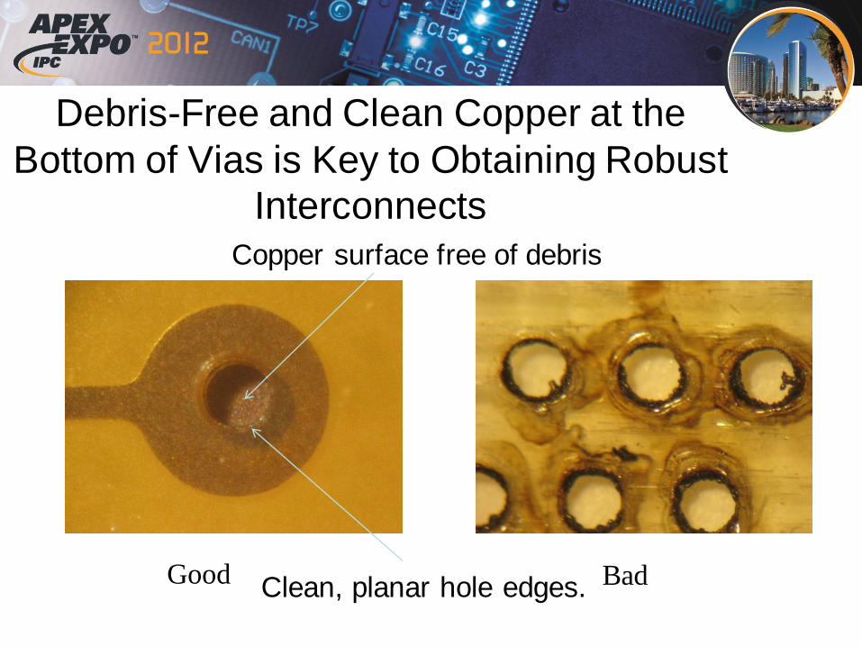
Debris-Free and Clean Copper at the
Bottom of Vias is Key to Obtaining Robust
Interconnects
Good Bad
Copper surface free of debris
Clean, planar hole edges.
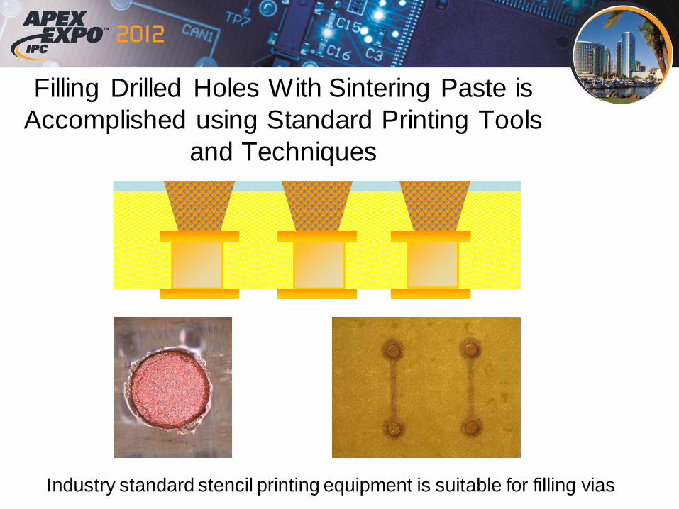
Filling Drilled Holes With Sintering Paste is
Accomplished using Standard Printing Tools
and Techniques
Industry standard stencil printing equipment is suitable for filling vias
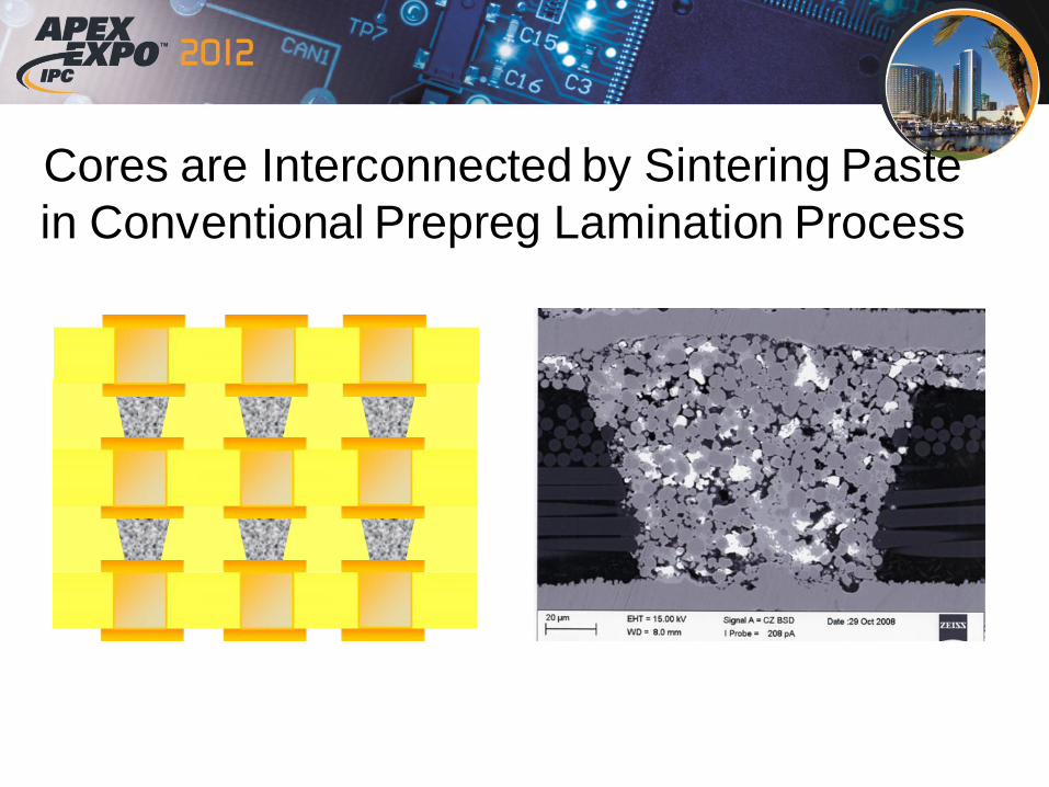
Cores are Interconnected by Sintering Paste
in Conventional Prepreg Lamination Process
Summary
• Electronic devices addressing high end computing, ATE, and military
applications can require high layer count PCBs with blind and buried vias
• Increasing interconnect density requirements are pushing designs to
utilize low yielding high-aspect-ratio PTHs
• High aspect ratio PTHs require complex drilling and plating processes,
and frequently add cost to the PCB through low yield
• Breaking high-aspect-ratio through holes up by manufacturing and
interconnecting subassembly ‘cores’ using paste interconnects is an
alternative technology to plating high aspect ratio PTHs
• Sintering conductive pastes are a reliable interconnect solution for
complex PCBs and enable lower costs, and higher yield compared to
plating
![Silicone Solutions for thermal management · 7 Thermally Conductive Dispensable Silicone Pads and Pastes Product Thermal Conductivity [W/mK] Type Viscosity D = 10 1/s [Pa.s] Hardness,](https://img.pdfslide.us/doc/110x75/5ec57351f2cf1c63373094ad/silicone-solutions-for-thermal-management-7-thermally-conductive-dispensable-silicone.jpg)