Embed Size (px)
Citation preview
PSpice with Cadence
1. Creating Circuits
2. AC Analysis
3. Step Response
4. Dependent Sources
5. Variable Phase VSin Source
Creating Circuits
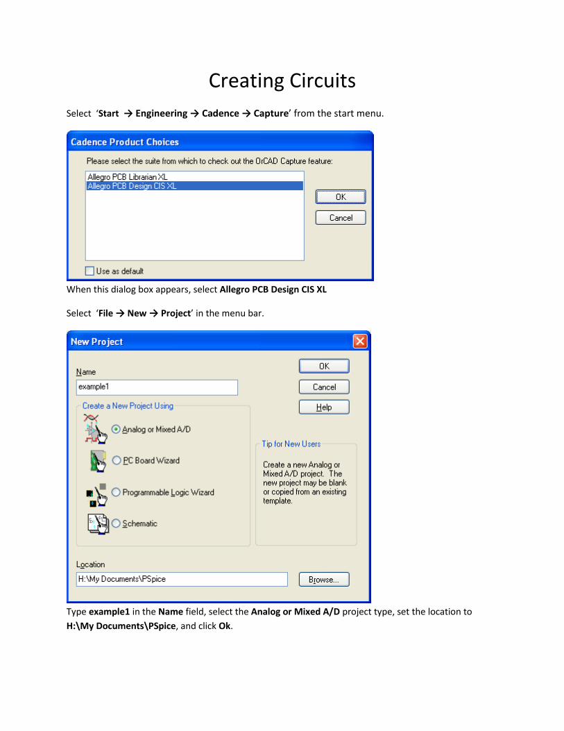
Select ‘Start → Engineering → Cadence → Capture’ from the start menu.
When this dialog box appears, select Allegro PCB Design CIS XL
Select ‘File → New → Project’ in the menu bar.
Type example1 in the Name field, select the Analog or Mixed A/D project type, set the location to
H:\My Documents\PSpice, and click Ok.
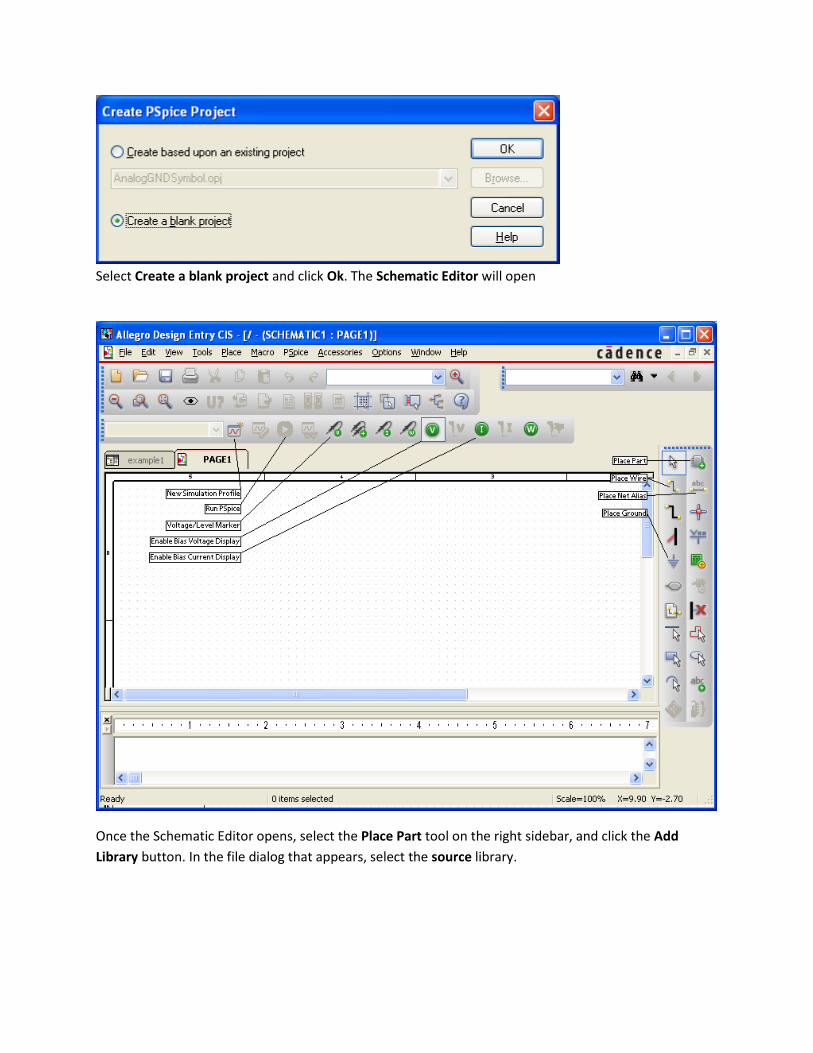
Select Create a blank project and click Ok. The Schematic Editor will open
Once the Schematic Editor opens, select the Place Part tool on the right sidebar, and click the Add
Library button. In the file dialog that appears, select the source library.
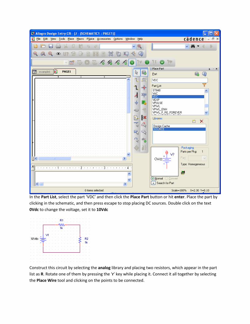
In the Part List, select the part ‘VDC’ and then click the Place Part button or hit enter. Place the part by
clicking in the schematic, and then press escape to stop placing DC sources. Double click on the text
0Vdc to change the voltage, set it to 10Vdc
Construct this circuit by selecting the analog library and placing two resistors, which appear in the part
list as R. Rotate one of them by pressing the ‘r’ key while placing it. Connect it all together by selecting
the Place Wire tool and clicking on the points to be connected.

In order to simulate a circuit, PSpice needs a ground node attached to it. Select the Place Ground tool in
the toolbar. Be warned that there are multiple libraries providing the ‘0’ symbol. Select the ‘Source’
library before selecting the ‘0’ symbol, then click Ok.
Place the ground symbol in the schematic and connect it to the circuit
Double click the resistance value of the horizontal resistor, and set it to ‘4k’.
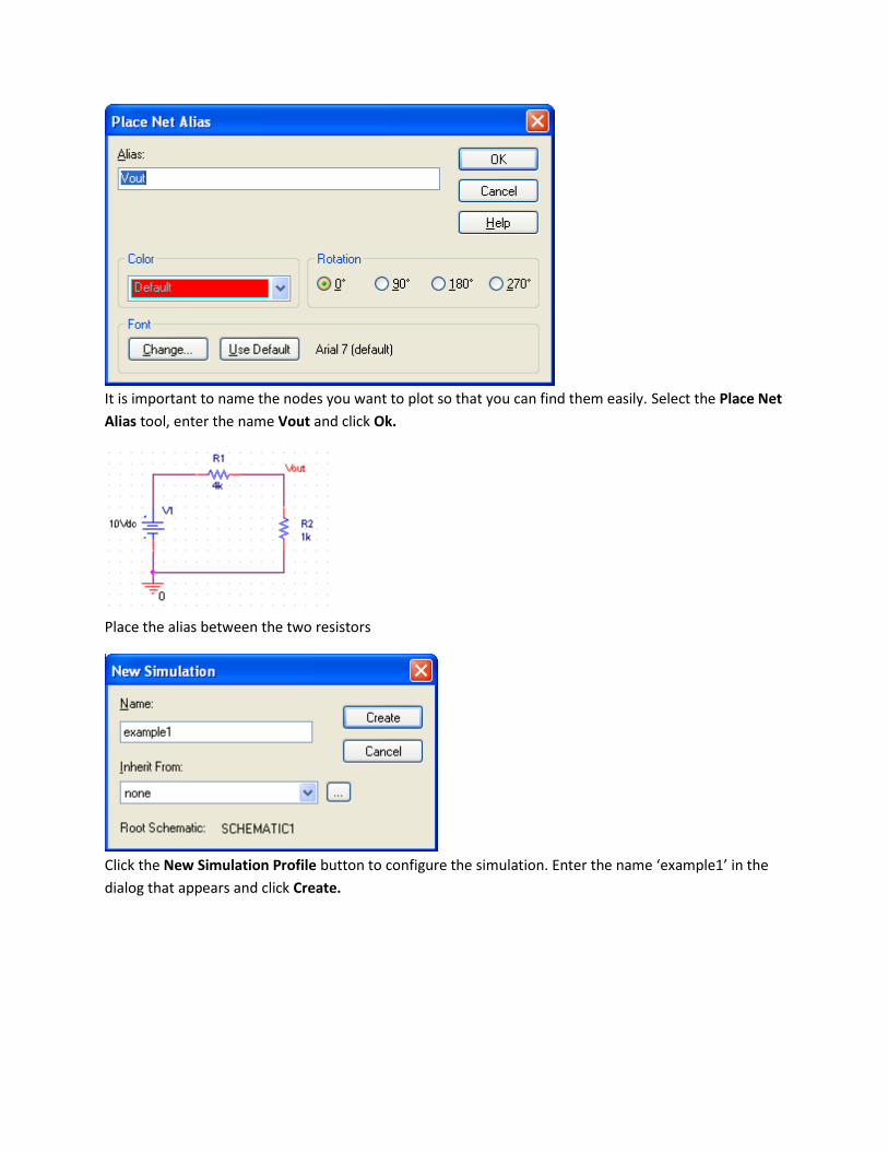
It is important to name the nodes you want to plot so that you can find them easily. Select the Place Net
Alias tool, enter the name Vout and click Ok.
Place the alias between the two resistors
Click the New Simulation Profile button to configure the simulation. Enter the name ‘example1’ in the
dialog that appears and click Create.

This will bring up the Simulation Settings dialog. Click Ok to accept the default settings.
Click on the Voltage/Level Marker button and place the marker on Vout as shown. Click the Run PSpice
button.
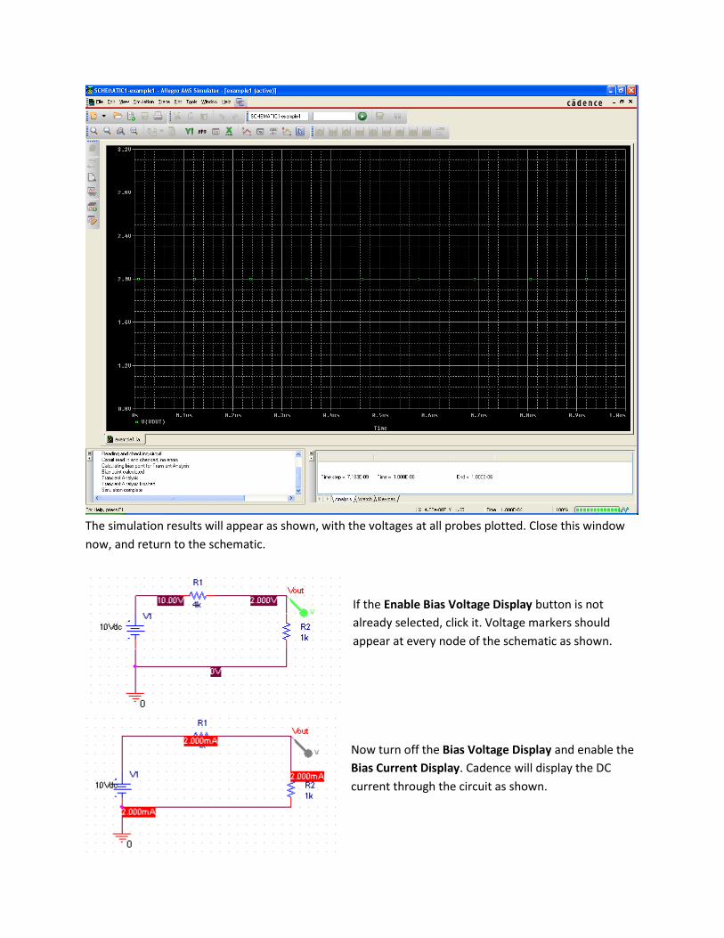
The simulation results will appear as shown, with the voltages at all probes plotted. Close this window
now, and return to the schematic.
If the Enable Bias Voltage Display button is not
already selected, click it. Voltage markers should
appear at every node of the schematic as shown.
Now turn off the Bias Voltage Display and enable the
Bias Current Display. Cadence will display the DC
current through the circuit as shown.
AC Circuit Analysis
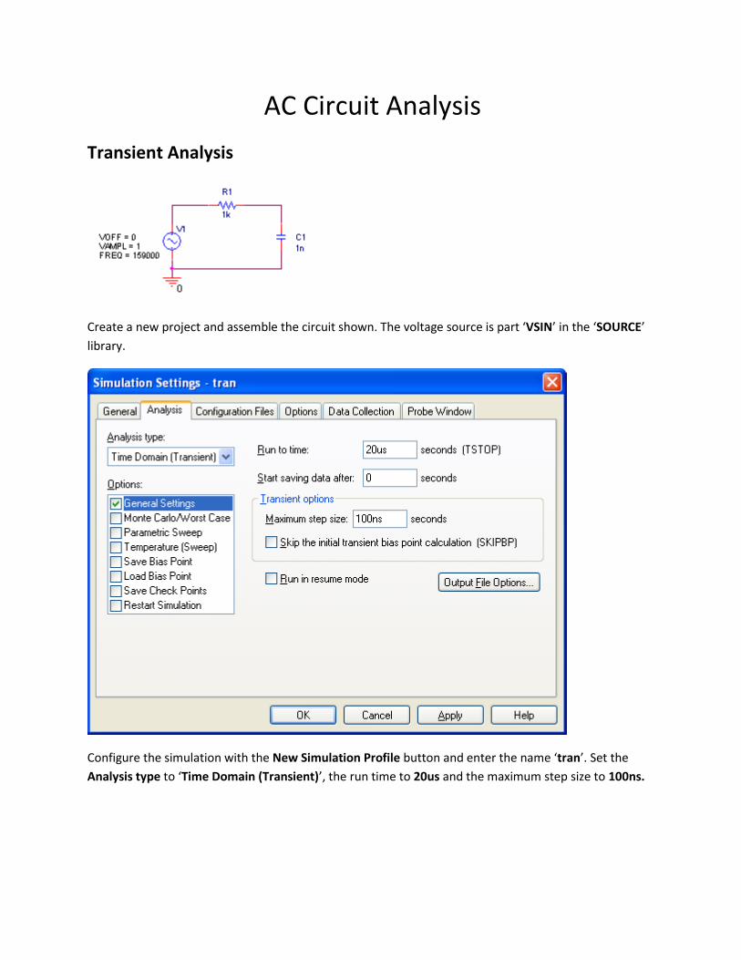
Transient Analysis
Create a new project and assemble the circuit shown. The voltage source is part ‘VSIN’ in the ‘SOURCE’
library.
Configure the simulation with the New Simulation Profile button and enter the name ‘tran’. Set the
Analysis type to ‘Time Domain (Transient)’, the run time to 20us and the maximum step size to 100ns.
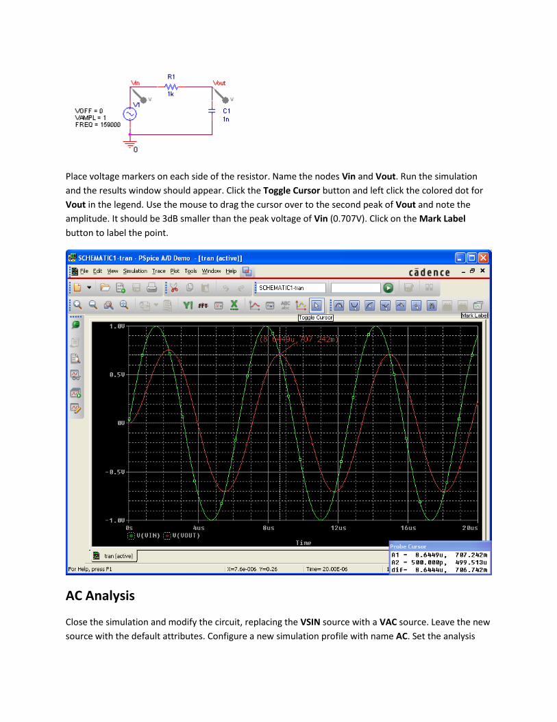
Place voltage markers on each side of the resistor. Name the nodes Vin and Vout. Run the simulation
and the results window should appear. Click the Toggle Cursor button and left click the colored dot for
Vout in the legend. Use the mouse to drag the cursor over to the second peak of Vout and note the
amplitude. It should be 3dB smaller than the peak voltage of Vin (0.707V). Click on the Mark Label
button to label the point.
AC Analysis
Close the simulation and modify the circuit, replacing the VSIN source with a VAC source. Leave the new
source with the default attributes. Configure a new simulation profile with name AC. Set the analysis
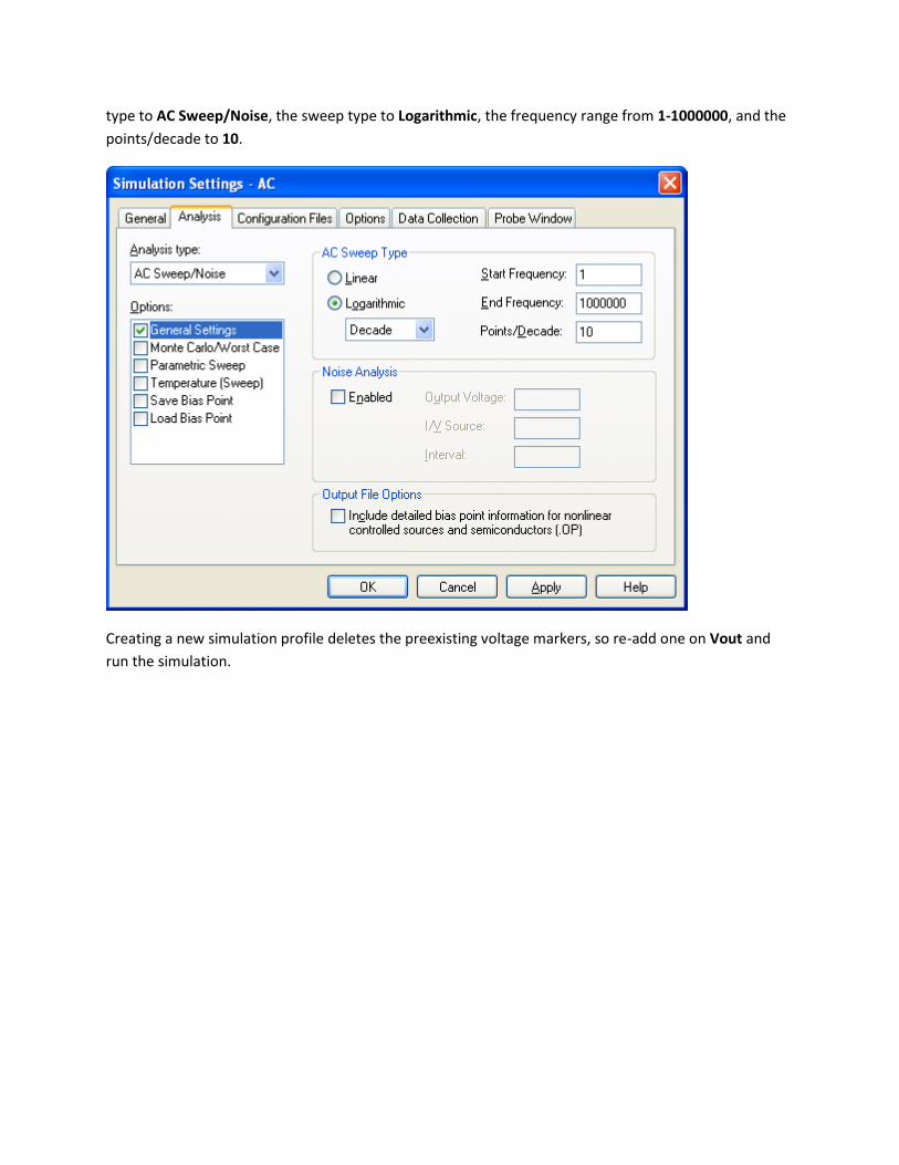
type to AC Sweep/Noise, the sweep type to Logarithmic, the frequency range from 1-1000000, and the
points/decade to 10.
Creating a new simulation profile deletes the preexisting voltage markers, so re-add one on Vout and
run the simulation.
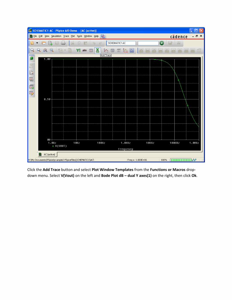
Click the Add Trace button and select Plot Window Templates from the Functions or Macros drop-
down menu. Select V(Vout) on the left and Bode Plot dB – dual Y axes(1) on the right, then click Ok.

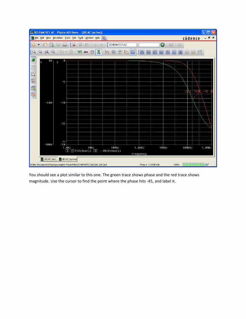
You should see a plot similar to this one. The green trace shows phase and the red trace shows
magnitude. Use the cursor to find the point where the phase hits -45, and label it.
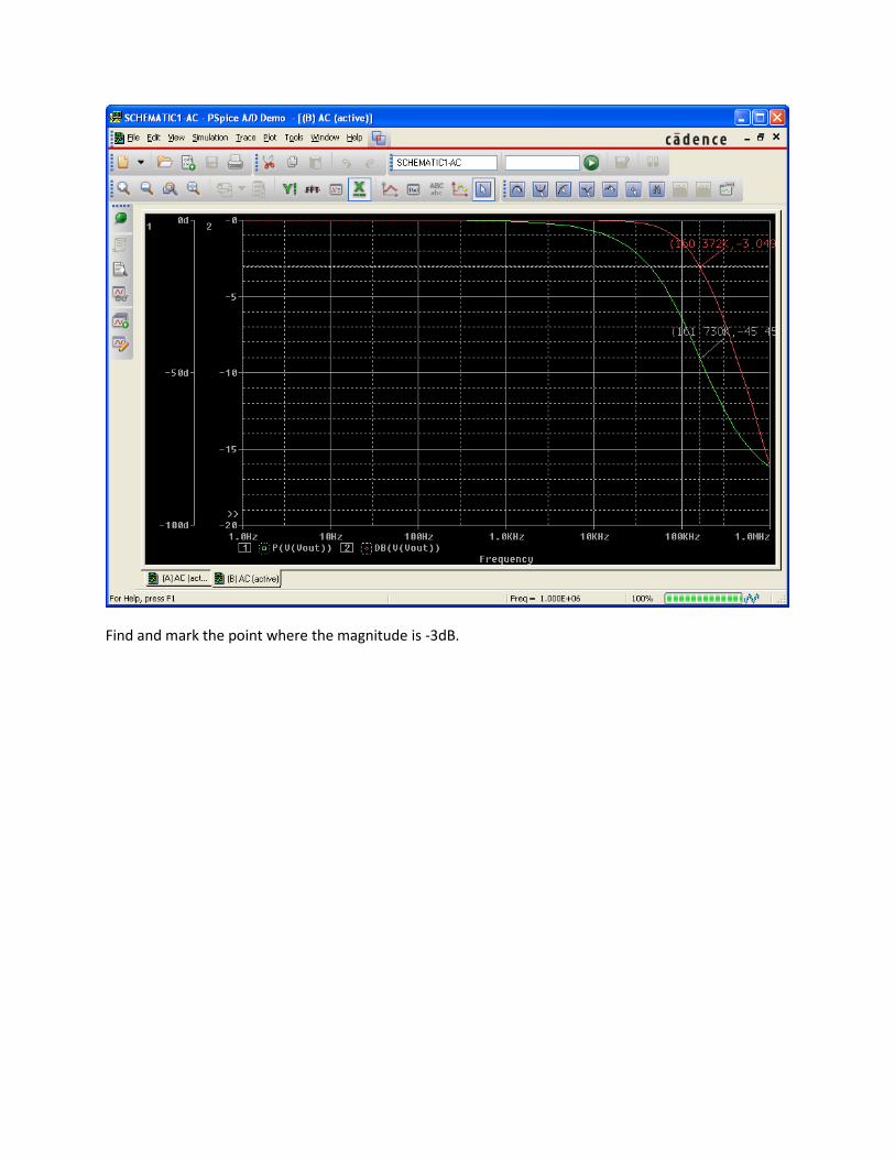
Find and mark the point where the magnitude is -3dB.

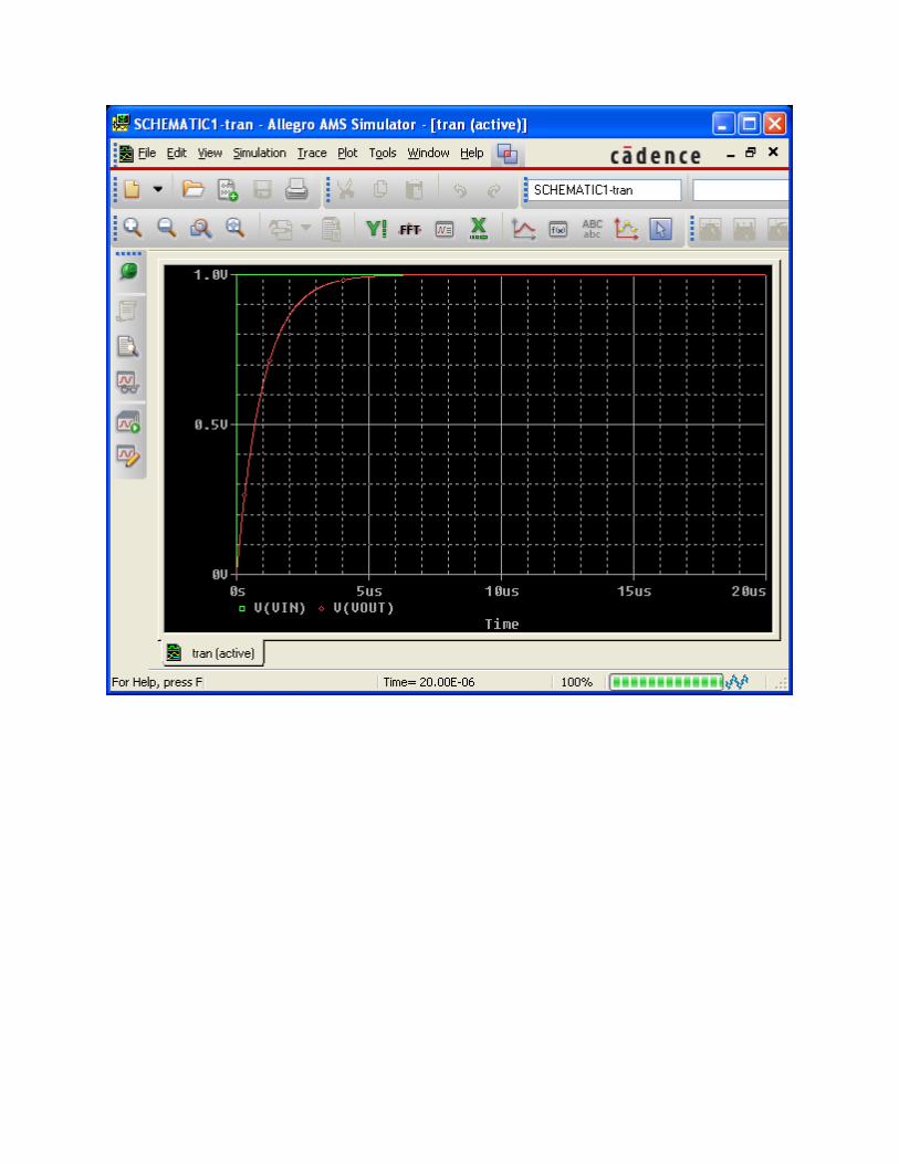
Step Response
To simulate a step response, create a new project and perform a transient analysis using the same steps
as above, but with a VPULSE voltage source. The VPULSE source has 7 parameters affecting the
waveform.
V1 = First Voltage
V2 = Second Voltage
TD = Initial Delay
TR = Absolute Rise Time
TF = Absolute Fall Time
PW = Pulse Width
PER = Period
To simulate a step response, we use a VPULSE source set to V1=0V, V2=1V, TD=0, TR=1ps, TF=1ps,
PW=1s, and PER=2s. A 1 picosecond rise/fall time is extremely small with regard to the simulation time,
so it closely approximates the ideal step function.
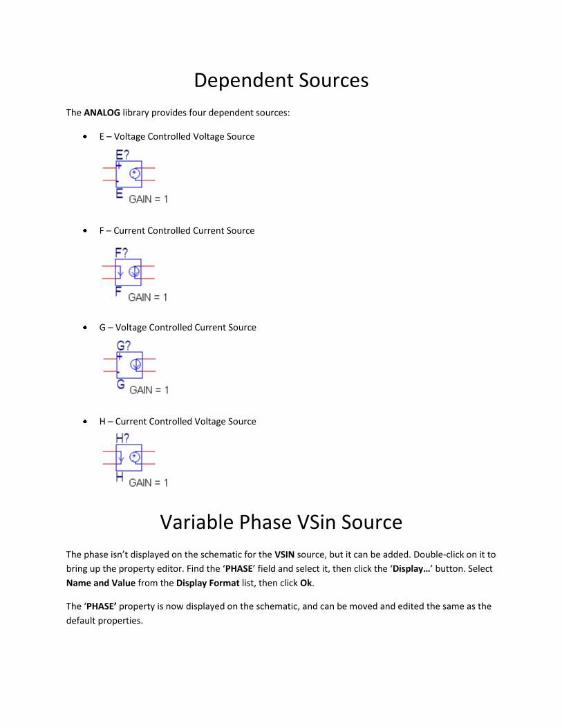
Dependent Sources
The ANALOG library provides four dependent sources:
E – Voltage Controlled Voltage Source
F – Current Controlled Current Source
G – Voltage Controlled Current Source
H – Current Controlled Voltage Source
Variable Phase VSin Source
The phase isn’t displayed on the schematic for the VSIN source, but it can be added. Double-click on it to
bring up the property editor. Find the ‘PHASE’ field and select it, then click the ‘Display…’ button. Select
Name and Value from the Display Format list, then click Ok.
The ‘PHASE’ property is now displayed on the schematic, and can be moved and edited the same as the
default properties.