Embed Size (px)
Citation preview

R08DS0131EJ0200 Rev.2.00 Page 1 of 18 Mar 11, 2016
Data Sheet
PS9031 2.5 A OUTPUT CURRENT, HIGH CMR, IGBT GATE DRIVE, 5-PIN SOP (LSO5 WITH 8mm CREEPAGE DISTANCE) PHOTOCOUPLER
DESCRIPTION
The PS9031 is an optically coupled isolator containing a GaAlAs LED on the input side and a photodiode, a signal processing circuit and power MOSFETs on the output side on one chip.
FEATURES
Long creepage distance (8 mm MIN.) Large peak output current (2.5 A MAX., 2.0 A MIN.) High speed switching (tPLH tPHL = 175 ns MAX.) UVLO (Under Voltage Lock Out) protection with hysteresis High common mode transient immunity (CMH, CML = 50 kV/s MIN.) Operating Ambient Temperature (125 C MAX.) Embossed tape product : PS9031-F3 : 3000 pcs/reel Pb-Free product Safety standards
UL approved: UL1577, Double protection CSA approved: CA5A, CAN/CSA-C22.2 No.60065, CAN/CSA-C22.2 No.60950-1, Reinforced insulation VDE approved: DIN EN 60747-5-5 (Option)
APPLICATIONS
IGBT, Power MOS FET Gate Driver Industrial inverter AC Servo
R08DS0131EJ0200Rev.2.00
Mar 11, 2016
Start of mass productionOct.2015
1. Anode2. Cathode3. VEE
4. VO
5. VCC
PIN CONNECTION(Top View)
5 3
1 2
4
SH
IELD

PS9031 Chapter Title
R08DS0131EJ0200 Rev.2.00 Page 2 of 18 Mar 11, 2016
PACKAGE DIMENSIONS (UNIT: mm)
Weight: 0.119g (typ.)
PHOTOCOUPLER CONSTRUCTION
Parameter MIN.
Air Distance 8.0 mm
Outer Creepage Distance 8.0 mm
Isolation Distance 0.15 mm

PS9031 Chapter Title
R08DS0131EJ0200 Rev.2.00 Page 3 of 18 Mar 11, 2016
BLOCK DIAGRAM
MARKING EXAMPLE
5
4
3
1
2
LED Output
ON H
OFF
Tr. 1
ON
OFF
Tr. 2
OFF
ON L
Input
H
L
SHIELD
(Tr. 2)
(Tr. 1)

PS9031 Chapter Title
R08DS0131EJ0200 Rev.2.00 Page 4 of 18 Mar 11, 2016
ORDERING INFORMATION
Part Number Order Number Solder Plating
Specification
Packing Style Safety Standard Approval
Application Part
Number*1
PS9031 PS9031-Y-AX Pb-Free and Halogen Free
(Ni/Pd/Au)
20 pcs (Tape 20 pcs cut) Standard products
(UL,CSA approved)
PS9031
PS9031-F3 PS9031-Y-F3-AX Embossed Tape 3 000
pcs/reel
PS9031-V PS9031-Y-V-AX 20 pcs (Tape 20 pcs cut) UL,CSA approved
DIN EN 60747-5-5
(VDE 0884-5): 2011-11 approved (Option)
PS9031-V-F3 PS9031-Y-V-F3-AX Embossed Tape 3 000
pcs/reel
Note: *1. For the application of the Safety Standard, following part number should be used.
ABSOLUTE MAXIMUM RATINGS (TA = 25C, unless otherwise specified)
Parameter Symbol Ratings Unit
Diode Forward Current IF 25 mA
Peak Transient Forward Current (Pulse Width < 1 s)
IF (TRAN) 1.0 A
Reverse Voltage VR 5 V
Power Dissipation *1 PD 45 mW
Detector High Level Peak Output Current *2 IOH (PEAK) 2.5 A
Low Level Peak Output Current *2 IOL (PEAK) 2.5 A
Supply Voltage (VCC VEE) 0 to 35 V
Output Voltage VO 0 to VCC V
Power Dissipation *3 PC 250 mW
Isolation Voltage *4 BV 5 000 Vr.m.s.
Operating Frequency f 200 kHz
Operating Ambient Temperature TA 40 to +125 C
Storage Temperature Tstg 55 to +150 C
Notes: *1. Reduced to 1.2 mW/C at TA = 110C or more.
*2. Maximum pulse width = 10 s, Maximum duty cycle = 0.2%
*3. Reduced to 3.9 mW/C at TA = 90C or more.
*4. AC voltage for 1 minute at TA = 25C, RH = 60% between input and output.
Pins 1-2 shorted together, 3-5 shorted together.
RECOMMENDED OPERATING CONDITIONS
Parameter Symbol MIN. TYP. MAX. Unit
Supply Voltage (VCC VEE) 15 30 V
Forward Current (ON) IF (ON) 8 10 12 mA
Forward Voltage (OFF) VF (OFF) 2 0.8 V
Operating Ambient Temperature TA 40 125 C

PS9031 Chapter Title
R08DS0131EJ0200 Rev.2.00 Page 5 of 18 Mar 11, 2016
ELECTRICAL CHARACTERISTICS
(at RECOMMENDED OPERATING CONDITIONS, VEE=GND, unless otherwise Specified) Parameter Symbol Conditions MIN. TYP.*1 MAX. Unit
Diode Forward Voltage VF IF = 10 mA, TA = 25C 1.35 1.56 1.75 V
Reverse Current IR VR = 3 V, TA = 25C 10 A
Input Capacitance CIN f = 1 MHz, VF = 0 V 30 pF
Detector High Level Output Current IOH VO = (VCC 4 V) *2 0.5 2.2 A
VO = (VCC 15 V) *3 2.0
Low Level Output Current IOL VO = (VEE + 2.5 V) *2 0.5 2.4 A
VO = (VEE + 15 V) *3 2.0
High Level Output Voltage VOH IO = 100 mA *4 VCC 3.0 VCC 1.3 V
Low Level Output Voltage VOL IO = 100 mA 0.2 0.5 V
High Level Supply Current ICCH VO = Open, IF = 10 mA 1.7 2.2 mA
Low Level Supply Current ICCL VO = Open, VF = 0 to 0.8V 1.7 2.2 mA
UVLO Threshold VUVLO+ VO > 5 V, IF = 10 mA 10.8 12.3 13.4 V
VUVLO 9.5 11.0 12.5
UVLO Hysteresis UVLOHYS VO > 5 V, IF = 10 mA 0.4 1.3 V
Coupled Threshold Input Current (L H)
IFLH IO = 0 mA, VO > 5 V 1.7 4.0 mA
Threshold Input Voltage (H L)
VFHL IO = 0 mA, VO < 5 V 0.8 V
Notes: *1. Typical values at TA = 25C, VCC VEE = 30 V.
*2. Maximum pulse width = 50 s, Maximum duty cycle = 0.5%.
*3. Maximum pulse width = 10 s, Maximum duty cycle = 0.2%.
*4. VOH is measured with the DC load current in this testing (Maximum pulse width = 2 ms, Maximum duty cycle = 20%).
SWITCHING CHARACTERISTICS
(at RECOMMENDED OPERATING CONDITIONS, VEE=GND, unless otherwise specified) Parameter Symbol Conditions MIN. TYP.*1 MAX. Unit
Propagation Delay Time (L H) tPLH Rg = 10 , Cg = 10 nF, 80 175 ns
Propagation Delay Time (H L) tPHL f = 10 kHz, 105 175 ns
Pulse Width Distortion (PWD) |tPHLtPLH| Duty Cycle = 50%, 25 75 ns
Propagation Delay Time (Difference Between Any Two Products)
tPHLtPLH IF = 10 mA 90 90 ns
Rise Time tr 40 ns
Fall Time tf 40 ns
Common Mode Transient Immunity at High Level Output
|CMH| TA = 25C, IF = 10 mA, VCC = 30 V, VCM = 1.5 kV
50 kV/s
Common Mode Transient Immunity at Low Level Output
|CML| TA = 25C, IF = 0 mA, VCC = 30 V, VCM = 1.5 kV
50 kV/s
Notes: *1. Typical values at TA = 25C, VCCVEE = 30 V.

PS9031 Chapter Title
R08DS0131EJ0200 Rev.2.00 Page 6 of 18 Mar 11, 2016
TEST CIRCUIT
Fig. 1 IOH Test Circuit Fig. 2 IOL Test Circuit
Fig. 3 VOH Test Circuit Fig. 4 VOL Test Circuit
Fig. 5 ICCH/ICCL Test Circuit
VCC
1.0 µF
1
2
IOL
1.0 µF
IF
VCC
1.0 µFVOH
100 mA
1.0 µF
IF
5
4
3IOH
VCC
1.0 µFVOL
100 mA
SHIELD
1
2
5
4
3
SHIELD
1
2
5
4
3
SHIELD
1
2
5
4
3
SHIELD
1
2
5
4
3
SHIELD
VCC
Fig. 6 UVLO Test Circuit
IF = 10 mA
VCC
1.0 µF
VO > 5 V
1
2
5
4
3
SHIELD
VCC

PS9031 Chapter Title
R08DS0131EJ0200 Rev.2.00 Page 7 of 18 Mar 11, 2016
VCCIF = 10 mA
10 kHz50% DUTYCYCLE
1.0 µF
VO10 Ω10 nF
tPHLtPLH
IF
VOUT
80%50%20%
tr tf
VCC = 30 V
VCM = 1.5 kV
1.0 µF
A
B
VO
IF
VOH
26 V
1 VVOL
VCM
0 V
VO
(Switch A: IF = 10 mA)
VO
(Switch B: IF = 0 mA)
Fig. 8 tPLH, tPHL, tr, tf Test Circuit and Wave Forms
Fig. 9 CMR Test Circuit and Wave Forms
tr
1
2
5
4
3
SHIELD
1
2
5
4
3
SHIELD
Fig. 7 IFLH Test Circuit
IF
VCC
1.0 µF
VO > 5 V
1
2
5
4
3
SHIELD
+ -
tr
1 500 V
10%
90%
PS9031 Chapter Title
R08DS0131EJ0200 Rev.2.00 Page 8 of 18 Mar 11, 2016
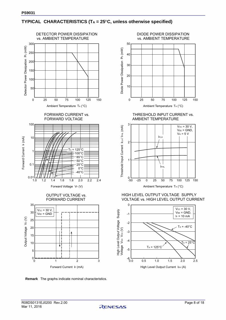
TYPICAL CHARACTERISTICS (TA = 25C, unless otherwise specified)
Remark The graphs indicate nominal characteristics.
Ambient Temperature TA (°C)
De
tect
or P
ow
er
Dis
sip
atio
n
PC (
mW
)
DETECTOR POWER DISSIPATION vs. AMBIENT TEMPERATURE
Ambient Temperature TA (°C)
Dio
de
Po
we
r D
issi
pat
ion
P
D (
mW
)
DIODE POWER DISSIPATION vs. AMBIENT TEMPERATURE
Ambient Temperature TA (°C)
Th
resh
old
In
put
Cu
rre
nt
IFLH
/ IF
HL (
mA
)
THRESHOLD INPUT CURRENT vs.AMBIENT TEMPERATURE
25 50 75 100 1501250
300
250
200
150
100
50
25 50 75 100 1501250
3
2
1
0
VCC = 30 V,VEE = GND,Vth = 5 V
-50 -25 100 12550 750 25 150
Forward Current IF (mA)
Out
putV
olta
ge
V
O (
V)
OUTPUT VOLTAGE vs.FORWARD CURRENT
100 2 3
35
30
25
20
15
10
5
50
40
30
20
10
Forward Voltage VF (V)
For
wa
rd C
urr
en
t IF
(m
A)
FORWARD CURRENT vs. FORWARD VOLTAGE
1.00.01
0.1
1
10
100
1.2 1.4 1.6 1.8 2.0 2.2 2.4
TA = 125°C100°C
85°C50°C25°C
0°C -40°C
Hig
h L
eve
l Out
putV
olta
ge
S
up
ply
Vo
ltag
e V
OH
VC
C (
V)
High Level Output Current IOH (A)
HIGH LEVEL OUTPUT VOLTAGE SUPPLYVOLTAGE vs. HIGH LEVEL OUTPUT CURRENT
0.0 0.5 1.0 1.5 2.52.0
0
-6
-5
-4
-3
-2
-1
TA = 25°C
TA = 125°C
TA = -40°C
IFLH
IFHL
VCC = 30 V,VEE = GND
VCC = 30 V,VEE = GND,IF = 10 mA

PS9031 Chapter Title
R08DS0131EJ0200 Rev.2.00 Page 9 of 18 Mar 11, 2016
Remark The graphs indicate nominal characteristics.
Forward Current IF (mA)
PROPAGATION DELAY TIME,PULSE WIDTH DISTORTIONvs. FORWARD CURRENT
PROPAGATION DELAY TIME,PULSE WIDTH DISTORTION
vs. SUPPLY VOLTAGE
Supply Voltage VCC (V)
Low Level Output Current IOL (A)
Low
Leve
lOut
putV
olta
geVO
L(V
)
LOW LEVEL OUTPUT VOLTAGE vs.LOW LEVEL OUTPUT CURRENT
Prop
agat
ion
Del
ayTi
me
tPH
L, tP
LH (n
s),
Puls
eW
idth
Dis
tort
ion
(PW
D)
t PH
L – tP
LH (n
s)
Prop
agat
ion
Del
ayTi
me
tPH
L, tP
LH (n
s),
Puls
eW
idth
Dis
tort
ion
(PW
D)
tPH
L – tP
LH (n
s)
Prop
agat
ion
Del
ayTi
me
tPH
L, tP
LH (n
s),
Puls
eW
idth
Dis
tort
ion
(PW
D)
t PH
L – tP
LH (n
s)
6 8 10 12 14 16
175
150
125
100
75
50
25
0
tPHL
PWD
tPLH
15 20 25 30
175
150
125
100
75
50
25
0
tPHL
PWD
tPLH
PROPAGATION DELAY TIME,PULSE WIDTH DISTORTION
vs. LOAD CAPACITANCE
Load Capacitance Cg (nF)
100 20 30 40 50
175
150
125
100
75
50
25
0
tPHL
tPLH
PWD
0.0 0.5 1.0 1.5 2.52.0
6
4
2
0
PROPAGATION DELAY TIME,PULSE WIDTH DISTORTIONvs. LOAD RESISTANCE
0 25 50 75
175
150
125
100
75
50
25
0
tPHL
PWD
tPLH
Load Resistance Rg (W)
Prop
agat
ion
Del
ayTi
me
tPH
L, tP
LH (n
s),
Puls
eW
idth
Dis
tort
ion
(PW
D)
t PH
L – tP
LH (n
s)
Prop
agat
ion
Del
ayTi
me
tPH
L, tP
LH (n
s),
Puls
eW
idth
Dis
tort
ion
(PW
D)
t PH
L – tP
LH (n
s)
PROPAGATION DELAY TIME,PULSE WIDTH DISTORTIONvs. AMBIENT TEMPERATURE
Ambient Temperature TA (°C)
0-50 -25 25 50 75 100
175
150
125
100
75
50
25
0
tPHL
tPLH
125 150
PWD
VCC = 30 V,VEE = GND,IF = 0 mA
TA = 25°C
TA = 125°C
TA = -40°C
VCC = 30 V, VEE = GND,Rg = 10 W, Cg = 10 nF,f = 10 kHz, Duty cycle = 50%
VEE = GND, IF = 10 mA,Rg = 10 W, Cg = 10 nF,f = 10 kHz, Duty cycle = 50%
VCC = 30 V, VEE = GND,IF = 10 mA, Rg = 10 W,f = 10 kHz, Duty cycle = 50%
VCC = 30 V, VEE = GND,IF = 10 mA, Cg = 10 nF,f = 10 kHz, Duty cycle = 50%
VCC = 30 V, VEE = GND,IF = 10 mA,Rg = 10 W, Cg = 10 nF,f = 10 kHz, Duty cycle = 50%

PS9031 Chapter Title
R08DS0131EJ0200 Rev.2.00 Page 10 of 18 Mar 11, 2016
Remark The graphs indicate nominal characteristics.
Ambient Temperature TA (°C)
SUPPLY CURRENT vs.AMBIENT TEMPERATURE
Hig
hLe
vel S
uppl
yCu
rren
t ICC
H (m
A),
Low
Leve
l Sup
ply
Curr
ent
ICCL (
mA
)
-25 0 25 50 10075-50
2.5
1.5
2.0
1.0
0.5
0.0125 150
ICCH
ICCL
Ambient Temperature TA (°C)
Supply Voltage VCC (V)
SUPPLY CURRENT vs.SUPPLY VOLTAGE
Hig
hLe
vel S
uppl
yCu
rren
t ICC
H (m
A),
Low
Leve
l Sup
ply
Curr
ent
I CCL (
mA
)
15 20 3025
2.5
2.0
0.0
0.5
1.0
1.5
ICCH (IF = 10 mA)
ICCL (IF = 0 mA)
Hig
hLe
velO
utpu
tVol
tage
– S
uppl
yVo
ltage
V OH –
VCC
(V)
HIGH LEVEL OUTPUT VOLTAGE – SUPPLYVOLTAGE vs. AMBIENT TEMPERATURE
0.0
-3.0
-2.5
-2.0
-1.5
-1.0
-0.5
-25 0 25 50 10075-50 125 150
-25 0 25 50 10075-50 125 150
-25 0 25 50 10075-50 125 150
-25 0 25 50 10075-50 125 150
Ambient Temperature TA (°C)
Hig
hLe
velO
utpu
tCur
rent
IO
H(A
)
HIGH LEVEL OUTPUT CURRENT vs.AMBIENT TEMPERATURE
Ambient Temperature TA (°C)
Low
Leve
lOut
putV
olta
geVO
L(V
)
LOW LEVEL OUTPUT VOLTAGE vs.AMBIENT TEMPERATURE
0.5
0.0
0.1
0.2
0.3
0.4
Ambient Temperature TA (°C)
Low
Leve
lOut
putC
urre
nt I
OL
(A)
LOW LEVEL OUTPUT CURRENT vs.AMBIENT TEMPERATURE
3.0
0.0
0.5
1.0
1.5
2.0
2.5
3.0
0.0
0.5
1.0
1.5
2.0
2.5
VCC = 30 V,VEE = GND,VO = OPEN
VEE = GND,VO = OPEN
VCC = 30 V, VEE = GND,IF = 10 mA, IO = –100 mA
VCC = 30 V, VEE = GND,IF = 10 mA, IO = 100 mA
VCC = 30 V, VEE = GND,IF = 10 mA, VCC–VO = 4 V
VCC = 30 V, VEE = GND,IF = 10 mA, VO = 2.5 V

PS9031 Chapter Title
R08DS0131EJ0200 Rev.2.00 Page 11 of 18 Mar 11, 2016
Remark The graphs indicate nominal characteristics.
OUTPUT VOLTAGE vs. SUPPLY VOLTAGE
Supply Voltage VCC – VEE (V)
Out
put V
olta
ge V
O (
V)
0 5 10 15 20
14
12
10
8
6
4
2
0
UVLOHYS
VUVLO+VUVLO−(12.3 V)(11.0 V)

PS9031 Chapter Title
R08DS0131EJ0200 Rev.2.00 Page 12 of 18 Mar 11, 2016
TAPING SPECIFICATIONS (UNIT: mm)
Packing:3000 pcs/reel
Tape Direction
Outline and Dimensions (Reel)
Outline and Dimensions (Taps)

PS9031 Chapter Title
R08DS0131EJ0200 Rev.2.00 Page 13 of 18 Mar 11, 2016
RECOMMENDED MOUNT PAD DIMENSIONS (UNIT: mm)
Remark All dimensions in this figure must be evaluated before use.

PS9031 Chapter Title
R08DS0131EJ0200 Rev.2.00 Page 14 of 18 Mar 11, 2016
NOTES ON HANDLING
1. Recommended soldering conditions (1) Infrared reflow soldering
• Peak reflow temperature 260C or below (package surface temperature) • Time of peak reflow temperature 10 seconds or less • Time of temperature higher than 220C 60 seconds or less • Time to preheat temperature from 120 to 180C 12030 s • Number of reflows Three • Flux Rosin flux containing small amount of chlorine (The flux
with a maximum chlorine content of 0.2 Wt% is recommended.)
(2) Wave soldering • Temperature 260C or below (molten solder temperature) • Time 10 seconds or less • Preheating conditions 120C or below (package surface temperature) • Number of times One (Allowed to be dipped in solder including plastic mold portion.) • Flux Rosin flux containing small amount of chlorine (The flux with a maximum chlorine
content of 0.2 Wt% is recommended.)
(3) Soldering by Soldering Iron • Peak Temperature (lead part temperature) 350C or below • Time (each pins) 3 seconds or less • Flux Rosin flux containing small amount of chlorine (The flux with a
maximum chlorine content of 0.2 Wt% is recommended.)
(a) Soldering of leads should be made at the point 1.5 to 2.0 mm from the root of the lead
(4) Cautions • Fluxes Avoid removing the residual flux with freon-based and chlorine-based cleaning solvent.
2. Cautions regarding noise
Be aware that when voltage is applied suddenly between the photocoupler’s input and output at startup, the output transistor may enter the on state, even if the voltage is within the absolute maximum ratings.
120±30 s(preheating)
220°C
180°C
Pac
kage
Sur
face
Tem
pera
ture
T (
°C)
Time (s)
Recommended Temperature Profile of Infrared Reflow
(heating)to 10 s
to 60 s
260°C MAX.
120°C

PS9031 Chapter Title
R08DS0131EJ0200 Rev.2.00 Page 15 of 18 Mar 11, 2016
USAGE CAUTIONS
1. This product is weak for static electricity by designed with high-speed integrated circuit so protect against static
electricity when handling.
2. Board designing
(1) By-pass capacitor of more than 1.0 F is used between VCC and GND near device. Also, ensure that the distance
between the leads of the photocoupler and capacitor is no more than 10 mm.
(2) When designing the printed wiring board, ensure that the pattern of the IGBT collectors/emitters is not too
close to the input block pattern of the photocoupler.
If the pattern is too close to the input block and coupling occurs, a sudden fluctuation in the voltage on the
IGBT output side might affect the photocoupler’s LED input, leading to malfunction or degradation of
characteristics.
(If the pattern needs to be close to the input block, to prevent the LED from lighting during the off state due to
the abovementioned coupling, design the input-side circuit so that the bias of the LED is reversed, within the
range of the recommended operating conditions, and be sure to thoroughly evaluate operation.)
3. Make sure the rise/fall time of the forward current is 0.5 s or less.
4. In order to avoid malfunctions, make sure the rise/fall slope of the supply voltage is 3 V/s or less.
5. Avoid storage at a high temperature and high humidity.

PS9031 Chapter Title
R08DS0131EJ0200 Rev.2.00 Page 16 of 18 Mar 11, 2016
SPECIFICATION OF VDE MARKS LICENSE DOCUMENT
Parameter Symbol Spec. Unit
Climatic test class (IEC 60068-1/DIN EN 60068-1) 40/125/21
Dielectric strength maximum operating isolation voltage Test voltage (partial discharge test, procedure a for type test and random test)Upr = 1.6 UIORM., Pd 5 pC
UIORM
Upr
1 130
1 808
Vpeak
Vpeak
Test voltage (partial discharge test, procedure b for all devices) Upr = 1.875 UIORM., Pd 5 pC
Upr 2 119 Vpeak
Highest permissible overvoltage UIOTM 8 000 Vpeak
Degree of pollution (DIN EN 60664-1 VDE0110 Part 1) 2
Comparative tracking index (IEC 60112/DIN EN 60112 (VDE 0303 Part 11)) CTI 400
Material group (DIN EN 60664-1 VDE0110 Part 1) II
Storage temperature range Tstg –55 to +150 °C
Operating temperature range TA –40 to +125 °C
Isolation resistance, minimum value VIO = 500 V dc at TA = 25°C VIO = 500 V dc at TA MAX. at least 100°C
Ris MIN. Ris MIN.
1012 1011
Safety maximum ratings (maximum permissible in case of fault, see thermal derating curve) Package temperature Current (input current IF, Psi = 0) Power (output or total power dissipation) Isolation resistance VIO = 500 V dc at TA = Tsi
Tsi Isi Psi
Ris MIN.
175 400 700
109
°C mA mW

PS9031 Chapter Title
R08DS0131EJ0200 Rev.2.00 Page 17 of 18 Mar 11, 2016

PS9031 Chapter Title
R08DS0131EJ0200 Rev.2.00 Page 18 of 18 Mar 11, 2016
Caution GaAs Products This product uses gallium arsenide (GaAs). GaAs vapor and powder are hazardous to human health if inhaled or ingested, so please observe the following points.
• Follow related laws and ordinances when disposing of the product. If there are no applicable laws and/or ordinances, dispose of the product as recommended below.
1. Commission a disposal company able to (with a license to) collect, transport and dispose of materials that contain arsenic and other such industrial waste materials.
2. Exclude the product from general industrial waste and household garbage, and ensure that the product is controlled (as industrial waste subject to special control) up until final disposal.
• Do not burn, destroy, cut, crush, or chemically dissolve the product.
• Do not lick the product or in any way allow it to enter the mouth.

Notice1. Descriptions of circuits, software and other related information in this document are provided only to illustrate the operation of semiconductor products and application examples. You are fully responsible for
the incorporation of these circuits, software, and information in the design of your equipment. Renesas Electronics assumes no responsibility for any losses incurred by you or third parties arising from the
use of these circuits, software, or information.
2. Renesas Electronics has used reasonable care in preparing the information included in this document, but Renesas Electronics does not warrant that such information is error free. Renesas Electronics
assumes no liability whatsoever for any damages incurred by you resulting from errors in or omissions from the information included herein.
3. Renesas Electronics does not assume any liability for infringement of patents, copyrights, or other intellectual property rights of third parties by or arising from the use of Renesas Electronics products or
technical information described in this document. No license, express, implied or otherwise, is granted hereby under any patents, copyrights or other intellectual property rights of Renesas Electronics or
others.
4. You should not alter, modify, copy, or otherwise misappropriate any Renesas Electronics product, whether in whole or in part. Renesas Electronics assumes no responsibility for any losses incurred by you or
third parties arising from such alteration, modification, copy or otherwise misappropriation of Renesas Electronics product.
5. Renesas Electronics products are classified according to the following two quality grades: "Standard" and "High Quality". The recommended applications for each Renesas Electronics product depends on
the product's quality grade, as indicated below.
"Standard": Computers; office equipment; communications equipment; test and measurement equipment; audio and visual equipment; home electronic appliances; machine tools; personal electronic
equipment; and industrial robots etc.
"High Quality": Transportation equipment (automobiles, trains, ships, etc.); traffic control systems; anti-disaster systems; anti-crime systems; and safety equipment etc.
Renesas Electronics products are neither intended nor authorized for use in products or systems that may pose a direct threat to human life or bodily injury (artificial life support devices or systems, surgical
implantations etc.), or may cause serious property damages (nuclear reactor control systems, military equipment etc.). You must check the quality grade of each Renesas Electronics product before using it
in a particular application. You may not use any Renesas Electronics product for any application for which it is not intended. Renesas Electronics shall not be in any way liable for any damages or losses
incurred by you or third parties arising from the use of any Renesas Electronics product for which the product is not intended by Renesas Electronics.
6. You should use the Renesas Electronics products described in this document within the range specified by Renesas Electronics, especially with respect to the maximum rating, operating supply voltage
range, movement power voltage range, heat radiation characteristics, installation and other product characteristics. Renesas Electronics shall have no liability for malfunctions or damages arising out of the
use of Renesas Electronics products beyond such specified ranges.
7. Although Renesas Electronics endeavors to improve the quality and reliability of its products, semiconductor products have specific characteristics such as the occurrence of failure at a certain rate and
malfunctions under certain use conditions. Further, Renesas Electronics products are not subject to radiation resistance design. Please be sure to implement safety measures to guard them against the
possibility of physical injury, and injury or damage caused by fire in the event of the failure of a Renesas Electronics product, such as safety design for hardware and software including but not limited to
redundancy, fire control and malfunction prevention, appropriate treatment for aging degradation or any other appropriate measures. Because the evaluation of microcomputer software alone is very difficult,
please evaluate the safety of the final products or systems manufactured by you.
8. Please contact a Renesas Electronics sales office for details as to environmental matters such as the environmental compatibility of each Renesas Electronics product. Please use Renesas Electronics
products in compliance with all applicable laws and regulations that regulate the inclusion or use of controlled substances, including without limitation, the EU RoHS Directive. Renesas Electronics assumes
no liability for damages or losses occurring as a result of your noncompliance with applicable laws and regulations.
9. Renesas Electronics products and technology may not be used for or incorporated into any products or systems whose manufacture, use, or sale is prohibited under any applicable domestic or foreign laws or
regulations. You should not use Renesas Electronics products or technology described in this document for any purpose relating to military applications or use by the military, including but not limited to the
development of weapons of mass destruction. When exporting the Renesas Electronics products or technology described in this document, you should comply with the applicable export control laws and
regulations and follow the procedures required by such laws and regulations.
10. It is the responsibility of the buyer or distributor of Renesas Electronics products, who distributes, disposes of, or otherwise places the product with a third party, to notify such third party in advance of the
contents and conditions set forth in this document, Renesas Electronics assumes no responsibility for any losses incurred by you or third parties as a result of unauthorized use of Renesas Electronics
products.
11. This document may not be reproduced or duplicated in any form, in whole or in part, without prior written consent of Renesas Electronics.
12. Please contact a Renesas Electronics sales office if you have any questions regarding the information contained in this document or Renesas Electronics products, or if you have any other inquiries.
(Note 1) "Renesas Electronics" as used in this document means Renesas Electronics Corporation and also includes its majority-owned subsidiaries.
(Note 2) "Renesas Electronics product(s)" means any product developed or manufactured by or for Renesas Electronics.
http://www.renesas.comRefer to "http://www.renesas.com/" for the latest and detailed information.
California Eastern Laboratories, Inc.4590 Patrick Henry Drive, Santa Clara, California 95054-1817, U.S.A.Tel: +1-408-919-2500, Fax: +1-408-988-0279Renesas Electronics Europe LimitedDukes Meadow, Millboard Road, Bourne End, Buckinghamshire, SL8 5FH, U.KTel: +44-1628-585-100, Fax: +44-1628-585-900Renesas Electronics Europe GmbHArcadiastrasse 10, 40472 Düsseldorf, Germany Tel: +49-211-6503-0, Fax: +49-211-6503-1327Renesas Electronics (China) Co., Ltd.Room 1709, Quantum Plaza, No.27 ZhiChunLu Haidian District, Beijing 100191, P.R.ChinaTel: +86-10-8235-1155, Fax: +86-10-8235-7679Renesas Electronics (Shanghai) Co., Ltd.Unit 301, Tower A, Central Towers, 555 Langao Road, Putuo District, Shanghai, P. R. China 200333 Tel: +86-21-2226-0888, Fax: +86-21-2226-0999Renesas Electronics Hong Kong LimitedUnit 1601-1611, 16/F., Tower 2, Grand Century Place, 193 Prince Edward Road West, Mongkok, Kowloon, Hong KongTel: +852-2265-6688, Fax: +852 2886-9022Renesas Electronics Taiwan Co., Ltd.13F, No. 363, Fu Shing North Road, Taipei 10543, TaiwanTel: +886-2-8175-9600, Fax: +886 2-8175-9670Renesas Electronics Singapore Pte. Ltd.80 Bendemeer Road, Unit #06-02 Hyflux Innovation Centre, Singapore 339949Tel: +65-6213-0200, Fax: +65-6213-0300Renesas Electronics Malaysia Sdn.Bhd.Unit 1207, Block B, Menara Amcorp, Amcorp Trade Centre, No. 18, Jln Persiaran Barat, 46050 Petaling Jaya, Selangor Darul Ehsan, MalaysiaTel: +60-3-7955-9390, Fax: +60-3-7955-9510Renesas Electronics India Pvt. Ltd.No.777C, 100 Feet Road, HAL II Stage, Indiranagar, Bangalore, IndiaTel: +91-80-67208700, Fax: +91-80-67208777Renesas Electronics Korea Co., Ltd.12F., 234 Teheran-ro, Gangnam-Gu, Seoul, 135-080, KoreaTel: +82-2-558-3737, Fax: +82-2-558-5141
SALES OFFICES
© 2016 Renesas Electronics Corporation. All rights reserved.Colophon 5.0


![neosid NeoTAG 3ICTyp-PI-0320-E · 2020-03-23 · [mm] P1 [mm] NeoTAG ® Inlay F/MF2626 6000 8.0 4.0 NeoTAG ® Inlay F/MF2659 2400 16.0 8.0 NeoTAG ® Plug FG8336 1200 16.0 12.0 NeoTAG](https://img.pdfslide.us/doc/110x75/5f893db19ba4b75edc46b8fd/neosid-neotag-3ictyp-pi-0320-e-2020-03-23-mm-p1-mm-neotag-inlay-fmf2626.jpg)