Embed Size (px)
Citation preview

1
Proton Test Guideline Development– Lessons Learned
Prepared by:Stephen Buchner, Paul Marshall, Scott Kniffin and Ken LaBel
NASA/Goddard Space Flight Center
For:
NASA Electronic Parts and Packaging (NEPP) ProgramElectronics Radiation Characterization (ERC) Project
And
Defense Threat Reduction Agency
Date: 8/22/02

2
Table of Contents
1.0 General Introduction…………………………………………………………….…… 52.0 Space Radiation Environment……………………………………………..…….….. 63.0 Proton Test Facilities……………………………………………………………..…. 9
3.1 High-Energy Test Facilities………………………………………………..…. 93.1.1 University of California, Davis………………………………………… 93.1.2 Texas A&M……………………………………………………………. 93.1.3 TRIUMF………………………………………………………………… 103.1.4 Indiana University Cyclotron Facility…………………………………... 103.1.5 Lawrence Berkeley Laboratories………………………………………... 113.1.6 Harvard Cyclotron Facility……………………………………………… 113.1.7 Loma Linda University Medical Center………………………………… 113.1.8 Other facilities…………………………………………………………... 11
3.2 Low-Energy Facilities…………………………………………………………. 113.2.1 NASA GSFC…………………………………………………………….. 12
3.3 Other Facilities Links………………………………………………………….. 124.0 Dosimetry……………………………………………………………………………. 13
4.1 Scintillators…………………………………………………………………….. 134.2 Secondary Electron Emission Monitors………………………………………. 134.3 Faraday Cup…………………………………………………………………... 144.4 Radiochromic Films…………………………………………………………… 144.5 Beam Degraders………..……………………………………………………… 15
5.0 General Lessons Learned…………………………………………………………….. 165.1 Radiation Safety……………………………………………………………….. 165.2 Safety Interlocks……………………………………………………………….. 165.3 Positioning the Device under Test…………………………………………….. 165.4 Use of Apertures……………………………………………………………….. 175.5 Remote Control of the Experiment……………………………………………. 175.6 Exposure in Air………………………………………………………………… 175.7 Protection of Support Equipment……………………………………………… 185.8 Secondary Neutrons…………………………………………………………… 185.9 Beam Control………………………………………………………………….. 185.10 Proton Energy Specification…………………………………………………… 195.11 Induced Radioactivity…………………………………………………………. 195.12 Food and Drink………………………………………………………………… 195.13 Shipping……………………………………………………………………….. 195.14 Booking Time………………………………………………………………….. 195.15 Beam Parameters………………………………………………………………. 19
5.15.1 Energy……………………………………………………………….. 195.15.2 Flux…………………………………………………………………… 205.15.3 Uniformity…………………………………………………………… 205.15.4 Fluence………………………………………………………………. 21
5.16 Range Calculations…………………………………………………………….. 216.0 Proton SEE Testing…………………………………………………………………… 24
6.1 Background……………………………………………………………………. 246.2 Proton Beam Parameters………………………………………………………. 28
6.2.1 Proton Energy………………………………………………………… 286.2.2 Proton Flux…………………………………………………………… 296.2.3 Proton Fluence……………………………………………………….. 29
6.3 Whether to Test………………………………………………………………… 29

3
6.4 Effects of Packaging…….................................................................................... 296.5 Beam Control………………………………………………………………….. 306.6 Special Concerns for Devices…………………………………………………. 30
6.6.1 SRAMs and DRAMs (Multiple Bit Upsets)…………………………. 306.6.2 Optical Detectors…………………………………………………….. 306.6.3 Single-Event Transients……………………………………………… 306.6.4 Power MOSFETs…………………………………………………….. 306.6.5 Stuck Bits in Memories (DRAMs and SRAMs)…………………….. 316.6.6 Epitaxial Devices (including SOI) with Small Dimensions…………. 316.6.7 Latchup………………………………………………………………. 316.6.8 Analog-to-Digital Converters………………………………………… 32
6.7 Testing at Speed……………………………………………………………….. 326.8 Number of Devices Tested…………………………………………………….. 326.9 Data Analysis………………………………………………………………….. 32
6.9.1 Bendel 1-Parameter Equation………………………………………… 326.9.2 Bendel 2-Parameter Equation………………………………………… 336.9.3 Weibull 4-Parameter Equation………………………………………. 336.9.4 Proton Energies…………………………………………………….... 346.9.5 Check on Results…………………………………………………….. 34
6.9.5.1 PROFIT…………………………………………………….. 346.9.5.2 Figure of Merit……………………………………………… 34
7.0 TID Issues and Lessons Learned…………………………………………………….. 357.1 Background……………………………………………………………………. 357.2 Calculation of Total Ionizing Dose……………………………………………. 387.3 Factors Affecting TID Damage………………………………………………… 39
7.3.1 Proton Energy………………………………………………………… 397.3.2 Testing Under Bias…………………………………………………… 39
7.4 Selection of Proton Flux……………………………………………………….. 397.5 Estimate of TID Levels before Testing………………………………………… 407.6 Monitoring TID Damage………………………………………………………. 407.7 Testing more than One Device………………………………………………… 407.8 Fluence and TID……………………………………………………………….. 407.9 Dose modified by Shielding…………………………………………………… 41
8.0 Displacement Damage Dose Testing………………………………………………… 428.1 Background……………………………………………………………………. 428.2 Proton Energy………………………………………………………………….. 468.3 Measurement of Displacement Damage Dose………………………………… 488.4 Damage Factor………………………………………………………………… 488.5 Separation of DDD and TID…………………………………………………… 488.6 Microdosimetry………………………………………………………………… 488.7 Time after Exposure before Effects of DD Measured…………………………. 498.8 Bias During Exposure…………………………………………………………. 498.9 Number of Devices…………………………………………………………….. 498.10 Presence of Background Neutrons…………………………………………….. 498.11 Flux…………………………………………………………………………….. 498.12 Shielding Calculations…………………………………………………………. 49
9.0 Combined Effects Testing…………………………………………………………….. 509.1 Discrete and Linear Bipolar Technologies……………………………………… 509.2 Optocouplers……………………………………………………...…………….. 519.3 Sensors………………………………………………………………………….. 549.4 CMOS Microcircuits……………………………………………………………. 59

4
9.5 GaAs and other High Speed Devices…………………………………………. .. 619.6 Hybrids, Board, and Box Level Testing with Mixed Technologies………….. .. 61
10.0 Summary………………………………………………………………………………. 6411.0 Acknowledgements……………………………………………………………………. 6412.0 References………………………………………..……………………………………. 65

5
1.0 General IntroductionElectronic, opto-electronic and optical components on board spacecraft must operate in a
radiation environment consisting of electrons and ions that span the periodic table from H to U.Exposure to those ions may cause significant damage to the components that reduce performanceand compromise the mission’s success. The actual fluxes encountered vary widely, depending onthe spacecraft orbit, solar activity and shielding.[BART97] In some regions of space, such as inthe van Allen belts surrounding the earth, the radiation environment consists of large fluxes ofelectrons and protons and, to a much lesser extent, heavy ions. Electrons cause damage primarilythrough spacecraft charging and total ionizing dose (TID). Protons, because they are highlypenetrating, relatively massive and present in large numbers, degrade the performance ofspacecraft components through TID and displacement damage (DD) as well as single-eventeffects (SEEs).
Candidate devices for future space missions should be radiation tested to assess whether theycan fulfill their intended application in the anticipated radiation environment. Because testing inspace is rarely practical or feasible due to the cost, time, difficulty and uncertainty involved,radiation test engineers use specialized equipment in terrestrial laboratories to generate andmeasure the types of damage that occur in space. To simulate the effects of proton-induceddamage, engineers use proton beams at accelerator facilities. The procedures employed duringproton testing depend on both the type of device being tested and the type of radiation damagebeing assessed. This “Lessons Learned” document is designed to serve as a guide for theradiation test engineer who needs to perform proton testing on parts being considered for use inspace. It is not intended to be a “test method” but it does contain information, such as protonenergy and fluence, which will, most likely, be included in any future “test method” document.Its purpose is as a guide to alert the radiation test engineer to issues that, if ignored, could lead toproblems or mistakes that are sometimes merely an inconvenience and at other times result inmisleading or inaccurate conclusions.
This document begins by describing those aspects of the space radiation environment relevantto protons, such as their energy spectra and how shielding modifies the spectra. Section 3provides a list of facilities at which proton testing can be done, and includes details about thefacility, such as contact person, beam properties, travel to the facility, proton energies availableetc. Dosimetry is often an issue, and Section 4 describes the three widely used dosimetrymethods. Section 5 contains a listing of guidelines and lessons learned that are applicable to allkinds of proton testing, such as the implications of testing in air, radiation safety issues, use ofapertures, proton-induced radioactivity, etc. Sections 6, 7 and 8 are all structured similarly. Eachsection begins with a detailed description of the mechanisms contributing to single-event effects(Section 6), total ionizing dose (Section 7) and displacement damage dose (Section 8). Followingthe introduction, each section contains a list of “lessons learned” specific to that type of test.Section 9 consists of a series of “Case Studies” that illustrate some of the difficulties encounteredin proton testing, such as the combination of total ionizing dose and displacement damage effects,or the effects of total ionizing dose on single event upset sensitivity. The final section contains asummary and conclusions.

6
2.0 Space Radiation EnvironmentBefore proceeding, it is instructive to consider an example of the space radiation environment
where the proton flux is known to exceed the heavy ion flux by many orders of magnitude. Thiswill illustrate why proton testing is important. Knowledge of the environment is essential forpredicting whether a device will survive the anticipated maximum flux and total fluence a spacemission is expected to encounter. A comprehensive discussion of the radiation environment inspace is beyond the scope of this monograph, and the interested reader is referred, instead, to anumber of excellent reviews. [BART97, DALY01, GARR93].
Figure 2.1 presents the proton spectrum calculated for low earth orbit (705 km altitude and98o inclination) behind various thickness of Al shielding. The unshielded spectrum was obtainedusing NASA’s AP8-MAX program.[BART97,SAWY76] The modified spectrum, followingpassage of the protons through the aluminum shielding, which represents the shielding affordedby the spacecraft itself, was calculated using another program, NOVICE. [JORD76] Notice that,in the absence of shielding, low-energy protons dominate and the spectrum extends out to a fewhundred MeV. With increasing shielding thickness, the low-energy proton fluence issignificantly reduced, while the fluence of protons with energies greater than 50 MeV is hardlyaffected. Evidently, shielding reduces the total proton flux by preferentially reducing thecontributions from low-energy protons that increase the average proton energy. As a result, thechoice of energies at which to test for TID, DD and SEE are partly determined by the amount ofshielding. Although shielding is effective at reducing the fluence of low-energy protons,secondary radiation is generated as a result of protons interacting with the shielding material.Secondary radiation takes the form of gamma rays, neutrons, protons, electrons, alpha particles,and heavier nuclei whose distributions depend on the initial proton energy and type of shieldingmaterial. Heavy metals, such as molybdenum or tantalum, sometimes used for shielding give riseto a greater flux of secondary particles. These secondary sources of radiation may makesignificant contributions to DD (up to 25%) and TID (up to 7%) in shielded devices and shouldtherefore not be ignored.[JUN01, JUN01b] Based on this discussion, it is a good idea to obtainthe shielded proton spectrum prior to doing proton testing to use as a guide in the selection ofproton energies.
Fig. 2.1 Trapped proton fluence for low-earth orbit as a function of energy for a number of differentthicknesses of aluminum shielding.[BART97]
The role of shielding in modifying the proton energy spectrum can be understood byinspecting Fig. 2.2, which shows how the proton’s energy loss per unit length (dE/dx) viaionization in aluminum depends on the proton’s energy. At low energy, the proton’s energy lossincreases rapidly until it reaches a maximum at 100 keV. Above 100 keV, the energy loss

7
decreases monotonically. Highly energetic protons lose relatively small amounts of energycompared with low-energy protons. For a given shielding thickness (a few millimeters), high-energy protons will lose much less energy than low-energy protons. In fact, many of the low-energy protons will not make it through the shielding, whereas the high-energy protons will passthrough with a relatively small reduction in energy. As a result, the proton energy spectrum willexhibit a preferential reduction in the number of low-energy protons, the relative size of thereduction depending on the thickness of the shielding material and on the flux of secondarysources of radiation.
0
0.1
0.2
0.3
0.4
0.5
100 101 102 103 104 105
Proton Energy (keV)
Ene
rgy
Loss
per
Uni
t Len
gth
(MeV
.cm
2 /mg)
Fig. 2.2. Proton energy loss in Si as a function of proton energy
Figure 2.3 shows how shielding reduces the total ionizing dose deposited by protons andelectrons in a device in low-earth orbit with altitude of 500 km and inclination of 51.6degrees.[MARS99] Included in this calculation are the contributions from secondary sources ofradiation. The figure clearly demonstrates that, for this case, increasing the shielding beyond 300mils is not effective in reducing the dose, because the high-energy protons are not eliminated byshielding. Because shielding cannot completely protect devices against proton-induced TID, DDor single-event effects, engineers are forced to do proton testing based on the shielding modifiedproton spectrum at the device.
Fig. 2.3. TID due to protons and electrons as a function of shielding thickness.[MARS99]

8
An engineer’s decision to do proton testing is typically motivated by one or more of thefollowing factors [MARS99]:
• There is no SEE or DD data available for parts that are going to be used in a proton-rich environment.
• Heavy-ion data suggests that the parts might be SEE-sensitive to protons because ofrelatively low LET thresholds.
• The parts are COTS devices, which frequently have large lot-to-lot variations in thedegree of DD degradation.
• The parts are in packages that cannot be de-lidded, making heavy ion testingimpossible, and one would like to get a general idea of their sensitivity to SEEs.
• There is neutron data on DD indicating marginal performance.• The parts may be sensitive to both TID and DD so that testing with 60Co will not give
the complete picture.• It is suspected that the parts may be sensitive to proton-induced SEEs via direct
ionization as is frequently the case for optical detectors used in fiber optic data linksor optocouplers.
• There is a possibility that the parts are sensitive to proton-induced latchup, which, inmany cases, is a “show stopper.”
Once the decision to do proton testing has been reached, the engineer proceeds to the next stage,which is to generate a test plan. At present there is no standard test plan for proton testing, so it isup to the engineer to generate one. In the planning stage that precedes proton testing, theengineer should consider the list of issues, detailed below. That list is culled from proton testingexperience gained over a period of many years. As such, the items constitute a list of “lessonslearned” that should prove useful to someone, particularly the novice, wishing to do protontesting. Some may seem obvious, but ignoring them could lead to inconvenience, delay andwasted money. Before proceeding, the importance of generating a proper test plan prior to protontesting is once again stressed.

9
3.0 Proton Test FacilitiesThe facilities available for proton testing can be divided into those that provide high-energy
protons with energies greater than 20 MeV and those that provide low-energy protons withenergies less than 10 MeV.
3.1 High-Energy Test Facilities3.1.1 University of California, Davis• Crocker Nuclear Lab: http://crocker.ucdavis.edu/• Contacts: Dr. Carlos Castaneda 530-752-4228,
http://crocker.ucdavis.edu/cnl/people/staff.htm• Accelerator: Isochronal Cyclotron• Energies: 1-68 MeV tunable, He beam is also available, degraders available. Beam
intensity adjusted by accelerator operator.• Beam Information: single user, beam spot is 3 cm radius or collimators for smaller size
and in other shapes, 22.5 MHz – 7 MHz AC, full pulse is 44.4 ns (high E) to 143 ns(low E), p+ pulse width is 1.5 ns, independent of energy
• Beam Location: Beam in air, in vault. Table for mounting experiments givescontrolled motion only vertically. Alignment of target achieved with pointer and withlaser beam. Not controllable remotely.
• User Interface: Computer driven by user, very user friendly• Additional Facilities for Users: electronics shop and machine shop with techs are
available to users• Work Area/Cabling: lab area with direct access to cable run, cable run of ~60 feet• Dosimetry: direct current read from foils compared with respect to faraday cup to
calculate #particles and then dose secondary electron emission monitors• How do you get there? Fly into Sacramento and drive WSW (about 20 minutes) on I-
80 South to Davis.
3.1.2 Texas A&M University (TAMU)• TAMU: http://cyclotron.tamu.edu/ and http://cyclotron.tamu.edu/ref/index.htm• Contacts: Dr. Henry Clark and Dr. Vladimir Horvat: 979-845-1411• Accelerator: K500 super conducting cyclotron• Energies: 8 – 70 MeV tunable and degraders in line. Beam intensity adjusted by
accelerator operator.• Beam Information: single user, beam spot is 1” diameter, 20 MHz AC beam, 50ns
pulse with ns p+ pulse• Beam Location: Beam in air, in vault or in 30”D x 30”H vacuum chamber.
http://cyclotron.tamu.edu/ref/layout.gif• Also see: http://cyclotron.tamu.edu/ref/in-air.htm and
http://cyclotron.tamu.edu/ref/chamber.htm• User Interface: Fully computer driven by user (SEUSS program) or accelerator operator
controlled.• Additional Facilities for Users: electronics shop and staffed machine shop are available
to users• Work Area/Cabling: cable run of 30 feet for in air irradiation or 4 feet for vacuum
chamber irradiation.• Dosimetry: Four/Five scintillator array. See:
http://cyclotron.tamu.edu/ref/measure.htm. A qualitative profile check withradiochromic film can be done upon request.
10
• How do you get there? http://cyclotron.tamu.edu/ref/local.htm• Facility refs: http://cyclotron.tamu.edu/publications.html and
http://cyclotron.tamu.edu/progress/2000-2001/5_2.pdf
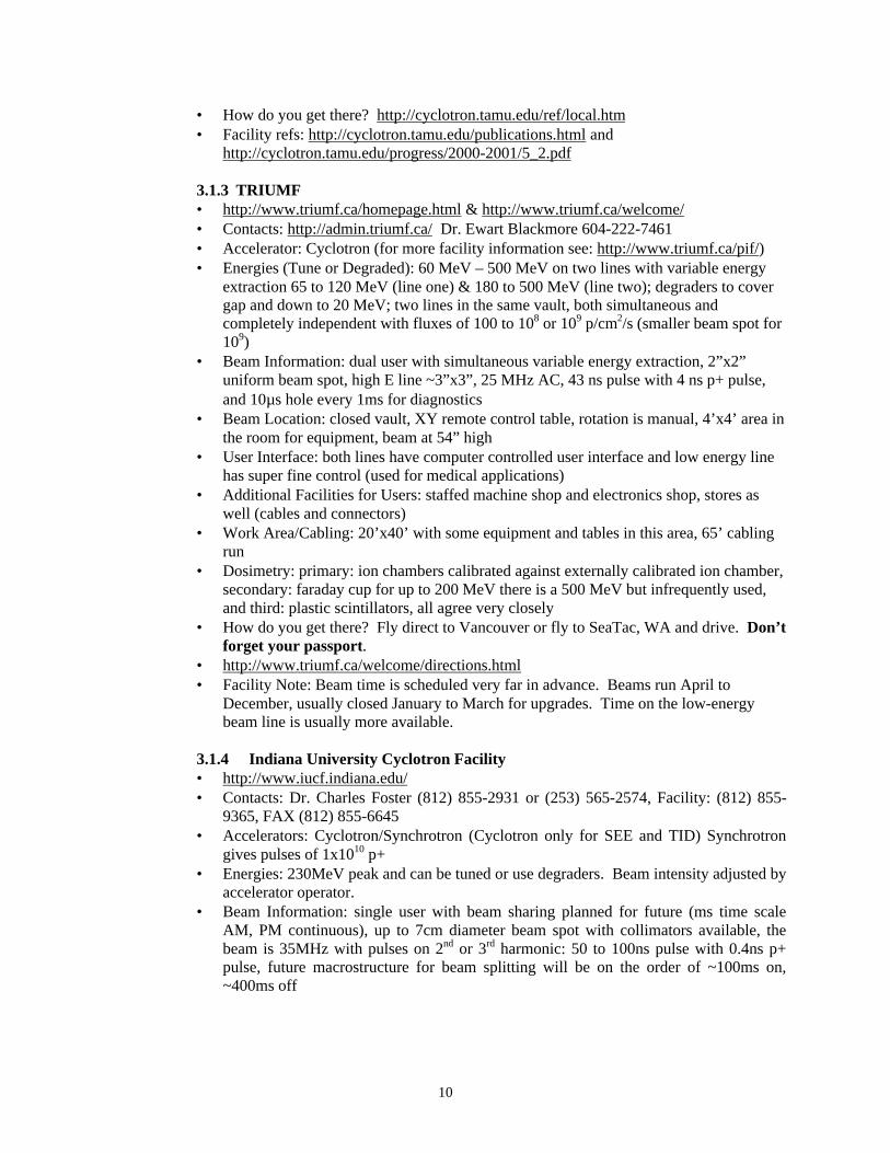
3.1.3 TRIUMF• http://www.triumf.ca/homepage.html & http://www.triumf.ca/welcome/• Contacts: http://admin.triumf.ca/ Dr. Ewart Blackmore 604-222-7461• Accelerator: Cyclotron (for more facility information see: http://www.triumf.ca/pif/)• Energies (Tune or Degraded): 60 MeV – 500 MeV on two lines with variable energy
extraction 65 to 120 MeV (line one) & 180 to 500 MeV (line two); degraders to covergap and down to 20 MeV; two lines in the same vault, both simultaneous andcompletely independent with fluxes of 100 to 108 or 109 p/cm2/s (smaller beam spot for109)
• Beam Information: dual user with simultaneous variable energy extraction, 2”x2”uniform beam spot, high E line ~3”x3”, 25 MHz AC, 43 ns pulse with 4 ns p+ pulse,and 10µs hole every 1ms for diagnostics
• Beam Location: closed vault, XY remote control table, rotation is manual, 4’x4’ area inthe room for equipment, beam at 54” high
• User Interface: both lines have computer controlled user interface and low energy linehas super fine control (used for medical applications)
• Additional Facilities for Users: staffed machine shop and electronics shop, stores aswell (cables and connectors)
• Work Area/Cabling: 20’x40’ with some equipment and tables in this area, 65’ cablingrun
• Dosimetry: primary: ion chambers calibrated against externally calibrated ion chamber,secondary: faraday cup for up to 200 MeV there is a 500 MeV but infrequently used,and third: plastic scintillators, all agree very closely
• How do you get there? Fly direct to Vancouver or fly to SeaTac, WA and drive. Don’tforget your passport.
• http://www.triumf.ca/welcome/directions.html• Facility Note: Beam time is scheduled very far in advance. Beams run April to
December, usually closed January to March for upgrades. Time on the low-energybeam line is usually more available.
3.1.4 Indiana University Cyclotron Facility• http://www.iucf.indiana.edu/• Contacts: Dr. Charles Foster (812) 855-2931 or (253) 565-2574, Facility: (812) 855-
9365, FAX (812) 855-6645• Accelerators: Cyclotron/Synchrotron (Cyclotron only for SEE and TID) Synchrotron
gives pulses of 1x10¹⁰ p+• Energies: 230MeV peak and can be tuned or use degraders. Beam intensity adjusted by
accelerator operator.• Beam Information: single user with beam sharing planned for future (ms time scale
AM, PM continuous), up to 7cm diameter beam spot with collimators available, thebeam is 35MHz with pulses on 2nd or 3rd harmonic: 50 to 100ns pulse with 0.4ns p+pulse, future macrostructure for beam splitting will be on the order of ~100ms on,~400ms off
11
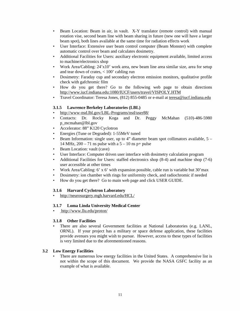
• Beam Location: Beam in air, in vault. X-Y translator (remote control) with manualrotation vise, second beam line with beam sharing in future (new one will have a largerbeam spot), both lines available at the same time for radiation effects work
• User Interface: Extensive user beam control computer (Beam Monster) with completeautomatic control over beam and calculates dosimetry.
• Additional Facilities for Users: auxiliary electronic equipment available, limited accessto machine/electronics shop
• Work Area/Cabling: 24’x10’ work area, new beam line area similar size, area for setupand tear down of crates, < 100’ cabling run
• Dosimetry: Faraday cup and secondary electron emission monitors, qualitative profilecheck with gafchromic film
• How do you get there? Go to the following web page to obtain directionshttp://www.iucf.indiana.edu:1080/IUCF/users/travel/VISPOLY.HTM
• Travel Coordinator: Teresa Jones, (812) 855-0485 or e-mail at [email protected]
3.1.5 Lawrence Berkeley Laboratories (LBL)• http://www-nsd.lbl.gov/LBL-Programs/nsd/user88/• Contacts: Dr. Rocky Koga and Dr. Peggy McMahan (510)-486-5980
[email protected]• Accelerator: 88” K120 Cyclotron• Energies (Tune or Degraded): 1-55MeV tuned• Beam Information: single user, up to 4” diameter beam spot collimators available, 5 –
14 MHz, 200 – 71 ns pulse with a 5 – 10 ns p+ pulse• Beam Location: vault (cave)• User Interface: Computer driven user interface with dosimetry calculation program• Additional Facilities for Users: staffed electronics shop (8-4) and machine shop (7-6)
user accessible at other times• Work Area/Cabling: 6’ x 6’ with expansion possible, cable run is variable but 30’max• Dosimetry: ion chamber with rings for uniformity check, and radiochromic if needed• How do you get there? Go to main web page and click USER GUIDE.
3.1.6 Harvard Cyclotron Laboratory• http://neurosurgery.mgh.harvard.edu/HCL/
3.1.7 Loma Linda University Medical Center• http://www.llu.edu/proton/
3.1.8 Other Facilities• There are also several Government facilities at National Laboratories (e.g. LANL,
ORNL). If your project has a military or space defense application, these facilitiesprovide avenues you might wish to pursue. However, access to these types of facilitiesis very limited due to the aforementioned reasons.
3.2 Low Energy Facilities• There are numerous low energy facilities in the United States. A comprehensive list is
not within the scope of this document. We provide the NASA GSFC facility as anexample of what is available.

12
3.2.1 NASA GSFC• http://radhome.gsfc.nasa.gov/radhome/ref/GSFC_REF.html• Contacts: Steve Brown 301-286-5795• Accelerators: two Van de Graaff accelerators, one solid-state accelerator• Energies (Tune or Degraded): both Van de Graaff accelerators are 100 keV to 1.7 MeV
tuned; the solid-state accelerator is tuned from 1 keV to 130 keV for a number ofelements and protons
• Beam Information: single user, all three are DC continuous beam• Beam Location: Van de Graaff accelerators are in vaults; one beam is in air or vacuum
chamber, the second is in vacuum chamber only, the solid-state accelerator is in a roomwith a vacuum chamber
• User Interface: accelerator operator controlled• Additional Facilities for Users: electronics shop available, limited machining capability• Work Area/Cabling: both Van de Graaff accelerators have about 16’x 8’ of experiment
space, the solid-state accelerator has 12’x8’, with more available if needed for all threeaccelerators. Cable runs are ~65’ for the damage Van de Graaff, 40’ for the calibrationVan de Graaff, and 3-10’ for the solid-state accelerator.
• Dosimetry: calibrated solid state barrier detectors
3.3 Other Facilities LinksBelow are web links to lists of other facilities in the US an abroad.
• Accelerator Labs Around the World: http://home.earthlink.net/~whittum/vl/labs.html• LINAC96 list of LINACs and related facilities:
http://linac96.web.cern.ch/Linac96/Linacs.html• Virtual Library of Accelerator User Facilities

13
4.0 DosimetryHigh-energy facilities rely on three primary dosimetry systems to determine the flux and
uniformity of the beam - scintillators (usually plastic/organic), secondary electron monitors andFaraday cups. Additionally, radiochromic films may be used to determine qualitatively beamuniformity. It is widely accepted that the dosimetry at most proton accelerators is reasonablyaccurate, at least within 10%.
4.1 ScintillatorsA scintillator detector is a device which, when exposed to ionizing radiation, converts a
portion of the incident particle energy into light. The scintillator response is directly proportionalto the energy lost by the incident particle. Photons produced in the interaction are detected by aphotomultiplier (PM) tube, which produces a current proportional to the light intensity. The lightis absorbed by a cathode consisting of a low work-function material at the front surface of the PMtube. Electrons are emitted from the cathode and accelerated to the first anode by the electricfield in the PM tube. Additional electrons are emitted by the anode and are accelerated to thenext anode at higher potential. There is a series of such anodes that together give a largeamplification or gain of the original signal. The gain can be greater than 106. The end result is adetectable electrical signal from even a single photon.[KNOL89] The scintillation detectors areplaced in an annular arrangement with respect to the beam for real time monitoring of the flux.Usually four scintillators are used (top, bottom, left and right). Additionally, a fifth one may beused that is moved in and out of the center of the beam for tuning and for a more precisedetermination of the flux. It is not uncommon for these scintillators to be made by the facility.
Figure 4.1. Representation of the function of a plastic scintillator. A portion of this image is from:http://www-numi.fnal.gov:8875/public/poster6.pdf
4.2 Secondary Electron MonitorsThese detectors function by passing the beam through a series of thin metal films (e.g.
aluminized Mylar). Interaction with the beam knocks secondary electrons free in the aluminumfoils, which are tied to a picoammeter. The current is proportional to the number of ions passingthrough the foils. An alternate setup that allows for the determination of the profile of the beamis possible as well. The foils are arranged such that alternating foils are positively biased and thefoils for detection are sandwiched in between these foils and are only aluminized on the top,bottom, left or right half. The display of the readings of each allows the operator to determine thebeam uniformity and focus.[CAST01]

14
Figure 4.2: Example of secondary electron monitors used at UCD Crocker Nuclear Labs [CAST01]
4.3 Faraday CupThe Faraday cup is as simple as it is elegant. The Faraday cup is essentially a well
surrounded by a magnetic field designed to capture the entire beam. In the case of protons, foreach ion entering the cup, an electron is pulled from ground through a current meter. Themagnetic field around the cup prevents secondary electrons inside the cup from escaping andprevents any produced externally from entering. Faraday cups are designed to be moved in andout of the beam or are placed in a separate area to provide measurements only when needed. Anexample of a motor driven one is provided below.
Figure 4.3. Picture and schematic of Faraday cup.Image from: http://www.casetechnology.com/implanter/faraday.html
4.4 Radiochromic FilmsRadiochromic films are frequently available for on-demand testing of a beam’s uniformity in
a purely qualitative manner. The film is exposed to a dose known not to saturate the film. Thefilm is then read by any number of means, but the most popular method is to scan the film with asimple flatbed scanner into a grayscale (0-255) image, and process it with a commerciallyavailable software package. One such program is Scion Software, available at

15
www.scioncorp.com. While this software package was originally developed for use in scanningPCR films in DNA research, it is well suited for use in this application. The software includes theability to look at a 3D plot of the beam spot and to do a histogram of any cross section of the filmdesired. Non-uniformities in the beam are immediately obvious.[CAST01],[JONE99]
4.5 Beam DegradersIt should be noted that if a degrader is positioned in front of the DUT, the dosimetry is
altered. The user must make the necessary corrections to allow for the broadening and shifting ofthe peak in the energy spectrum as a result of energy loss that depends on the type of materialused in the degrader as well as its thickness. For more on the use of degraders, see Sections5.15.1, 5.16, 6.2.1, and 6.5.3.

16
5.0 General Lessons LearnedLessons learned that are of a general nature and apply to all types of proton testing, including
SEE, TID or DDD are detailed in this section. They include radiation safety, device alignment,remote control of the experiment, range calculations, shipping equipment and booking time.
5.1 Radiation SafetyRadiation safety is of paramount importance because of the serious health hazards resulting
from exposure to the radiation present during proton testing. Testing is accomplished by placingthe DUT in front of an exit port on the test chamber. The protons reach the DUT after passingthrough a thin membrane from the vacuum into air and both the primary protons and thesecondary particles, such as neutrons, generated when the protons collide with any material, posea significant health hazard. Another source of radiation is the material activated by the protonswith a half-life that depends on the type of material – materials composed of low Z elements,such as Al, generally have short half-lives (minutes), whereas heavy materials, such as Au, willhave much longer half-lives (days). The dangers associated with exposure to radiation precludeanyone from being present in the vault when the beam is on. Once the beam has been turned off,the radiation test engineer should enter the room with a Geiger counter to monitor the radiationlevel. (Note that the danger to humans is related to the radiation dose, which is the product ofproton flux and exposure time.) Because of the legal issues involved, no safe exposure levels aregiven in this monograph, and the test engineer is advised to consult the radiation health physicistat the facility if any issues arise. Before being allowed into the vault, some facilities require thatthe test engineer take a rudimentary radiation safety course that consists, at a minimum of adescription of what to do in an emergency. (Although not required in the United States, someEuropean proton test facilities require test personnel to have a radiation physical prior to doingthe test. Without the relevant documents proving that you have had a radiation physical, you willnot be allowed to perform radiation testing.) All facilities require anyone entering a radiationfacility to wear a radiation “badge” at all times to monitor total radiation exposure. Make sure thefacility gives you one before you begin to work in any areas marked as a potential radiationhazard.
5.2 Safety InterlocksAfter the experiment has been set up and everything is ready, the last thing to do is to set the
safety interlocks. They are designed to ensure that no one is inadvertently left in the vault afterthe door is closed. In some facilities there are flashing lights and in others loud beeping soundssignaling that the interlocks have been activated. Make sure an accelerator staff member showsyou how to operate the interlocks and explains what to do if you are inadvertently left in thetesting room. Failure to activate the interlocks prior to leaving the vault will prevent the beamstop from being removed and no testing can be done until the interlocks have been set correctly.All facilities have a “panic” button in the vault so that if, by chance, the beam is turned on whilesomeone is still in the vault, touching the button will immediately switch the beam off.
5.3 Positioning the Device Under Test (DUT)The board containing the DUT must be securely mounted in front of the exit port. One
method is to clamp the board in a vice provided either by the facility or the radiation testengineer. Avoid clamping where there are exposed electrical wires or connectors that could shortout through the metal vice. At UCD, the vice sits on a table that can move in the verticaldirection. Movements in the x and y directions are done by hand. The vice must, in turn, besecured to the table using, for example, C-clamps. Proton testing at non-normal incidence is onlyrarely done so that few facilities have stages capable of rotating the DUT while still keeping it inthe center of the beam. If testing at non-normal incidence is necessary, you might have to bringalong your own goniometer. Alignment is critical to make sure the DUT is positioned in the

17
center of the beam, where uniformity is best, particularly when the DUT is rotated away fromnormal incidence. At UCD alignment is achieved either with a mechanical pointer attached to thecover that protects the port window or with vertical and horizontal laser beams that cross at thecenter of the beam.
5.4 Use of AperturesApertures are used to limit proton-induced damage to other devices adjacent to the DUT.
They fit over the exit port and consist of thick aluminum covers that contain holes of varioussizes and shapes to limit the extent of the beam. It is advisable to use the apertures even whenthere are no other devices adjacent to the DUT. The apertures limit exposure to the proton beamof both the board to which the device is attached and the mounting hardware, and so minimizesactivation of heavy metals, such as gold, used on the board. After high proton fluences, theapertures are activated and should not be handled until the radioactivity has decreased toacceptable levels.
5.5 Remote Control of the ExperimentAs already mentioned, the presence of high fluxes of radiation in the radiation exposure room
requires that engineers not be present during testing. Therefore, DUTs must be controlledremotely using long cables passed through tubes in the thick concrete walls of the vault. Forexperiments at UC Davis and IUC, the cables need to be about 50 feet in length. In addition, mostfacilities have patch panels with BNC connectors both inside and outside the vault. The BNCconnectors are labeled to facilitate connecting test equipment inside the vault with otherequipment, such as computers, in the room where the test engineers sit. Various approaches canbe used for remotely controlling the DUT, such as local area networks or bus extenders. Somefacilities have CCD cameras in the radiation exposure room that are connected to monitorslocated where test personnel work during a test run. They can be used, for example to monitorthe current supply for a DUT because increases in supply current are one manifestation of TIDdegradation. (See Section 7.1) This is often easier than monitoring a power supply outside theradiation exposure room, for which the voltage drop along a long cable (~50′) must beconsidered.
5.6 Exposure in AirThe rate of energy loss in material for high-energy (>20 MeV) protons is sufficiently low that
testing can be done in air. The proton beam travels down the vacuum tube to the exit port whereit passes through a thin window and intervening air gap with minimal energy loss. The fact thatthe exposure takes place in air greatly facilitates testing devices that require cooling because a fanis often sufficient to cool the DUT, thereby avoiding the use of water cooling in a vacuum. Inaddition, DUTs can be exchanged relatively quickly because it is not necessary to bring a vacuumchamber up to air and then pump it down again. The energy lost by the protons passing throughthe window material and the air between the window and the DUT must be taken into account atlow proton energies (below 20 MeV). The presence of the thin window membrane on theaccelerator exit port mandates that great care be exercised when aligning the DUT so as not topuncture the membrane. If the membrane is punctured, there will be a loud implosion as thevacuum is rapidly lost. This could result in damage to both the accelerator and the DUT as wellas injury to the test engineer. Furthermore, there would likely be a significant delay before theaccelerator could be brought on-line again, a delay that could prevent any more testing during thescheduled time. To avoid breaking the thin film, the exit port should be kept covered duringalignment and the cover removed only at the very last moment. Forgetting to remove the cover isa frequent mistake, and although it does not do anything to the device, it can waste precious time.This frequent error can be avoided by aiming a CCD camera in the vault to include the exit portto facilitate checking remotely whether the cover has been removed. This avoids having to go

18
back into the chamber after all the safety interlocks have been set and the door closed to checkwhether the cover is still on the exit port.
5.7 Protection of Support EquipmentScattered radiation, including neutrons and protons, present in the chamber during testing can
damage sensitive equipment used to exercise the DUT, especially if the equipment is locatedclose to the proton beam. Any equipment required to be in the radiation chamber should bepositioned away from the beam, and shielded with good neutron absorbers, such as lead bricks orboxes of Borax. This precaution is particularly important when high proton fluences areanticipated or when the equipment is to be used for many experiments. Figure 5.1 shows howboxes of Borax have been placed to protect an expensive power supply. Borax contains boron,which has a high absorption cross-section for neutrons, making it an effective neutron absorber.
Fig. 5.1. Boxes of Borax being used to shield the power supply against stray neutrons during proton testingat UC Davis.
5.8 Secondary NeutronsThe proton beam striking the DUT is contaminated with neutrons generated as a result of
protons interacting with the foils of the secondary electron emission monitor (SEEM), thewindow material and air molecules between the window and the DUT. The neutron flux istypically four orders of magnitude lower than the proton flux so that its contributions to radiationdamage of the DUT are usually ignored. [BERG97] Only where there is thick shieldingconsisting of heavy metals do neutrons make a significant contribution.
5.9 Beam ControlIn some cases, such as at UC Davis, the control room hands over limited control of the beam
to the test engineers. The test engineer determines when to turn the beam on and off, and alsocalibrates the SEEM and corrects for electronic noise in the SEEM. The control room maintainscontrol over the flux, which is specified prior to the run by the test engineers. The control roomalso removes and inserts the beam stop at the beginning and end of each run. When the beamstop is out, entry to the experimental chamber is forbidden. Request that a staff member showyou how to use the computer. You should also ask the staff member to explain how to continue arun following a sudden drop out of the beam, which happens on occasion. Following a run, thebeam parameters, including dose, fluence, exposure time, average beam current, etc should berecorded either as a hard copy or on floppy disk. Bring along a storage medium such as a floppy

19
disk to store the file. At other facilities, such as IUCF, accelerator personnel control all aspects ofthe irradiation and provide a hard copy of beam statistics for each run. TAMU will e-mail thefiles.
5.10 Proton Energy SpecificationThe proton energy available from a cyclotron depends on the cyclotron frequency, which is
set by the accelerator operator. Before it reaches the DUT, the protons first pass through a metalfoil to scatter the beam so that it covers a larger area and has improved uniformity. There is asmall energy loss as it passes through the foil. Next, the beam passes through a secondaryelectron emission monitor (SEEM) consisting of a series of metal foils used to measure the beamflux, and again there is a small energy loss. The beam then passes through the window materialand finally through a few centimeters of air before reaching the DUT. As an example of theenergy loss, the proton energy at UCD drops from 67 MeV in the accelerator down to 63 MeV atthe DUT if the DUT is positioned at the location indicated by the pointer on the exit port cover.Make sure that when you specify the proton energy you know which one you are specifying.
5.11 Induced RadioactivityThe use of heavy metals in test fixtures should be avoided because they have long radioactive
half-lives when activated. Aluminum is the material of choice because of its short half-life. Partscontaining heavy metal that have been tested to high fluences may require considerable timebefore they can be safely handled. In particular, radiated devices that are radioactive cannot beremoved from the site and must remain there until they can be shipped. Consult acceleratorfacility personnel. At the end of the experiment, most facilities require that all devices exposed tothe proton beam be tested for radioactivity, so do not pack any DUTs until their radioactivity hasbeen tested by facility personnel.
5.12 Food and DrinkBecause of the potential of radiation contamination, food is not allowed in any areas where
there is a possibility of radioactive dust settling on the food. Keep food outside the experimentalchamber. Furthermore, if you have worked in the experimental chamber, it is a good idea to washyour hands to remove any activated dust before handling any food.
5.13 ShippingBring along prepaid shipping documents so that your equipment can be returned on time.
Most facilities are helpful when it comes to return shipping. However, if you anticipate finishingup late at night when there is no staff in the office, arrange for return shipping during the day,before the staff go home.
5.14 Booking TimeIt is important that you contact the accelerator facility well ahead of the anticipated testing
date, because beam time is frequently at a premium. Furthermore, you may not be able to do anytesting without a contract in place with the facility. Contract sometimes takes months to finalizeand it is important that the process be started well ahead of the test data.
5.15 Beam ParametersFor any experiment it is necessary to specify proton energy, flux, uniformity and fluence.
5.15.1 EnergyThe proton energy used for testing is determined by the type of experiment (SEE, TID or DD)and will be discussed in greater detail in the appropriate section. The proton energy can beset either by tuning the cyclotron’s frequency or by placing degraders in the beam.

20
Degraders are slabs of material that reduce the proton energy by a fixed amount depending onthe slab’s thickness and composition. Degraders are best made from low Z material such asAl and Lexan to minimize activation. As will be pointed out in section 5.16, straggle must beconsidered, especially if thick degraders are used to reduce the proton’s energy by a largefraction.
5.15.2 FluxFlux is determined in part by the cost of beam time and by the capacity of the test equipmentto gather the relevant data. This will be discussed in greater detail in later sections. The fluxis determined by the beam current, which is measured in amperes. The average protoncurrent at UCD ranges from about 0.1 pA (2x10⁴ particles/sec/cm2 or 2 mrads(Si)/sec for 63MeV protons) to 100 nA (2x10¹⁰ particles/sec/cm2, equivalent to a dose rate of about 2x10³
rads(Si)/s). The minimum flux is limited by the SEEM. The SEEM measures current thatflows between two sets of foils in the vacuum. Protons passing through the SEEM ejectelectrons that are collected by foils maintained at positive bias. If the noise in the SEEM iscomparable to the beam current, the accuracy of the dosimetry is compromised. On the otherhand, very high proton fluxes (>1010 /cm2) are known to heat the DUT, which may affectparameters being monitored. For instance, heating can affect the annealing rate of TIDdamage.
5.15.3 UniformityBeam uniformity is important, particularly if more than one device at a time is to be tested, orif the device is comparable in size to the beam. The accelerator operator should measurebeam uniformity at the beginning of a run using radiochromic dye film. After exposure to apredetermined proton fluence, the radiochromic dye film is scanned to determine uniformity.From the scanned figure, corrections to the fluence as a function of distance from the center
Fig. 5.2 Correction factors used for the UC Davis proton beam as determined by scanning of aradiochromic dye film.[CAST01]
of the beam can be obtained. Fig. 5.2 shows the correction factors used at UCDavis.[CAST01] The figure shows that within a radius of 2 cm from the center of the beam,the fluence varies by about 5% and within a radius of 3 cm it varies by about 10%. Beamuniformity is also monitored in “real time” by the accelerator operators using an array of fourscintillator detectors placed around the edge of the beam. If the beam drifts, smalladjustments can be made to return it to its optimum position.

21
5.15.4 FluencePrior to starting an exposure, the test engineer should have an idea of the fluence required fora particular test based on the predicted fluence the part is expected to experience in space.Because of margin requirements, the parts are usually tested to fluences greater than whatthey will be exposed to in space. There are two approaches to testing. In the first, the fluenceor dose is applied in incremental steps and the part tested after each step. This is usuallynecessary when doing single-event upset (SEU) testing, or TID testing when checking theDUT for damage takes such a long time to complete that after checking the device will haveaccumulated a significant increment in dose. The TID damage is then plotted as a function ofeither fluence or dose. The second method involves monitoring the relevant parametersduring exposure. This is typically done when testing for single-event latchup (SEL). It mayalso be done for TID testing by continuously monitoring the leakage current. In the case ofSEU testing, the total fluence is determined by statistics. For example, if one is satisfied withdata having statistical error bars of 10%, the fluence should be such that at least 100 SEUs aredetected, because the statistical variations typically scale as N0.5. During SEL testing, it isfrequently necessary to turn the beam off while power to the part is being recycled. Failure todo so means additional fluence would be accumulated during a period when the DUT was notsensitive to SEL. One way to avoid this problem is to keep the flux sufficiently low that verylittle additional fluence is added between the time the part latches and the time the beam isturned off. The facility at UCD provides hard copies of all the relevant parameters for eachrun, including exposure time, beam current, proton energy, run number, uniformity,incremental fluence, incremental dose, total fluence and total dose. The maximum fluence isdetermined by the type of test being conducted. For SEE testing, the maximum fluence is setby the desired SEE statistics, whereas for TID and DD testing, the fluence is determineddirectly by the environment.
5.16 Range CalculationsHow far a proton penetrates through matter depends on the proton’s energy and on the
electronic and nuclear characteristics of the target material. The calculations are sufficientlycomplex that computer programs based on a Monte Carlo approach are used. One such programis SRIM2000, available free on the web. [ZIEG96] The program consists of two modules, 1)stopping power/range and 2) TRIM, which is a Monte Carlo simulation of the proton-matterinteraction. The first module calculates stopping powers via ionizing and non-ionizinginteractions as well as ranges of ions in matter. Table 5.1 lists the ion energy, ionizing energyloss, non-ionizing energy loss, range, longitudinal straggle and lateral straggle. The table showsthat 60 MeV protons have an electronic linear energy transfer (LET) in Si of 0.008596 MeV-cm2/mg and a range of 1.685 cm. With increasing energy, the range increases but the initial LETdecreases. Fig 2.2 shows graphically the energy loss due to ionization over a much wider rangethan that covered by Table 5.1. The web site for Brookhaven National Laboratory’s SEU facilitycontains a downloadable program for calculating LET for any incident ion into most targetmaterials (http://tvdg10.phy.bnl.gov/index.html).
The table also shows that energy losses via nuclear interactions (that lead to DD effects) arethree orders of magnitude lower than energy losses via ionization for the same proton energies.This column includes only Coulomb scattering and ignores inelastic scattering, leading to anunderestimation of the total amount of DD at higher proton energies. The reader is cautionedagainst using it for calculations of displacement damage dose for proton energies above 8MeV.[MARS99]

22
Table 5.1 SRIM2000 Output for Protons in Silicon.Ion Energy dE/dx
ElectronicdE/dx
NuclearProjected
RangeLong.
StragglingLateral
Straggling1.00 MeV 1.781E-1 1.328E-4 15.68 um 7591 A 9379 A5.00 MeV 5.866E-2 3.297E-5 215.28 um 9.53 um 10.22 um10.00 MeV 3.479E-2 1.786E-5 708.58 mm 32.69 um 31.64 um20.00 MeV 2.029E-2 9.614E-6 2.39 mm 98.56 um 101.57 um30.00 MeV 1.476E-2 6.677E-6 4.91 mm 212.97 um 203.18 um40.00 MeV 1.177E-2 5.150E-6 8.19 mm 328.13 um 333.14 um50.00 MeV 9.895E-3 4.208E-6 12.18 mm 530.91 um 489.13 um60.00 MeV 8.596E-3 3.566E-6 16.85 mm 723.37 um 669.25 um70.00 MeV 7.641E-3 3.100E-6 22.15 mm 916.42 um 871.86 um80.00 MeV 6.909E-3 2.476E-6 28.07 mm 1.26 mm 1.10 mm90.00 MeV 6.329E-3 2.467E-6 34.56 mm 1.58 mm 1.34 mm
100.00 MeV 5.857E-3 2.241E-6 41.62 mm 1.89 mm 1.60 mm120.00 MeV 5.135E-3 1.897E-6 57.32 mm 2.50 mm 2.18 mm140.00 MeV 4.609E-3 1.648E-6 75.01 mm 3.12 mm 2.82 mm160.00 MeV 4.208E-3 1.458E-6 94.54 mm 3.74 mm 3.52 mm180.00 MeV 3.893E-3 1.309E-6 115.79 mm 4.37 mm 4.26 mm200.00 MeV 3.637E-3 1.189E-6 138.63 mm 5.50 mm 5.06 mm
The second module, TRIM, can be used to calculate the energy loss as a function of distanceinto the silicon. To do that one must specify that TRIM save the ionization data to a file, whichcan then be plotted. Figure 5.3 shows an example of the ionizing energy loss per unit lengthversus depth in silicon for 20 MeV protons. This information is sufficient to calculate the chargedensity per unit length in the charge track generated by the proton. A useful conversion factor isthat a LET of 96 MeV-cm2/mg is equivalent to a linear charge density of 1 pC/µm. Thisconversion factor may be used to show that a 60 MeV proton has a LET of 0.0085 MeV-cm2/mgand produces a linear charge density of approximately 0.1 fC/µm.
Fig. 5.3. Linear energy loss for protons in Si as a function of distance from the Si surface.

23
SRIM2000 can also be used to calculate the average proton energy loss after passing though afinite thickness of material, information that is needed for determining the thickness of degradersused to reduce proton energy without having to retune beam energy. This can be done using theTRIM module. For instance, if one wishes to reduce the energy of a 100 MeV proton beam to 50MeV using an aluminum degrader, a calculation of stopping power and range for 100 MeVprotons in aluminum should first be done. The calculation shows that the range is 36.92 mm.Next one takes a guess for the aluminum thickness, say 20 mm, and the TRIM calculation iscarried out for an arbitrary number of ions, (200 ions is a reasonable number). For thecalculation, one must specify that a file containing the transmitted ions be generated. The resultsof the calculation show that the average energy of the protons is too high. A thicker degrader isthen tried and the calculation repeated. One eventually finds that 26 mm of aluminum reducesthe average proton energy from 100 MeV to 50.2 MeV. The results can also be used to calculatethe energy straggle. The file generated for this calculation lists the energies of the 200transmitted protons. The energies differ slightly because of the statistical nature of the proton-atom interactions. First the average energy of all 200 protons is calculated and then the standarddeviation. In this case the straggle is approximately 2 MeV. If necessary, the stopping power andrange of the 50.2 MeV protons in silicon can be calculated. Also, nuclear interactions need not beconsidered because the associated energy loss is about three orders of magnitude less than forionizing energy loss.
There is another way to calculate the energy of a particle after passing through a finitethickness of material. For this approach it is best to use the program from Brookhaven NationalLaboratory because smaller energy steps can be selected compared with the fixed larger energysteps provided by SRIM. The smaller step sizes improve the accuracy. Table 5.1 shows how tocalculate the energy of a 60 MeV proton after passing through 8.66 mm of silicon. The range of a60 MeV proton is 16.85 mm. If 8.66 mm are subtracted, 8.19 mm are left. The table shows thatthe energy of a proton with a range of 8.19 mm is 40 MeV. That is the energy of the emergingproton.

24
6.0 Proton SEE TestingThe underlying mechanisms responsible for most proton-induced SEEs differ from those for
heavy-ion induced SEEs. Heavy ions cause SEEs by direct ionization, whereas most protons firstundergo a nuclear interaction and the products of the interaction subsequently produce SEEs viadirect ionization. (The exceptions would be large devices, such as photodetectors, in whichprotons can generate sufficient charge by direct ionization to produce SEEs when they travelthrough the device at grazing angle of incidence). Because nuclear interactions are involved,testing for proton-induced SEEs involves measuring the cross-section as a function of protonenergy, and not as a function of linear energy transfer (LET) as is normally done for heavy-ions.Only in the case of photodetectors or, possibly, advanced devices on very thin epitaxial layers areangular measurements necessary to ascertain whether SEEs occur via direct ionization. In thissection we will first describe how SEEs are generated by protons and then present a list ofsuggestions to guide the experimenter doing proton SEE testing.
6.1 BackgroundWhen ions, including protons, pass through materials such as semiconductors and insulators,
they collide with the electrons and nuclei of the constituent atoms, losing energy in the process.Protons scatter elastically off the electrons through electromagnetic forces, whereas they scatterboth elastically (via electromagnetic and nuclear forces) and inelastically (via nuclear forces) offthe nuclei. The largest cross-section, by far, is that for proton-electron scattering, in which theenergy lost by protons liberates electrons bound to their host atom, producing free electron-hole(e-h) pairs that form a track of charge in the ion’s wake. The linear charge density along the trackcan be calculated from the ratio of energy loss per unit length and the average energy (Eg)required to generate one e-h pair (Eg = 3.6 eV in Si). The energy loss per unit length is obtainedfrom the normalized energy loss, termed linear energy transfer (LET), which can be obtainedfrom SRIM2000, as discussed in Section 5.14. As a result of diffusive forces, the e-h pairs in thetrack spread out laterally in a matter of picoseconds before ultimately recombining or beingcollected at junctions.
Electric fields present in semiconductor p/n junctions and gate oxides of MOSFETs separatethe e-h pairs generated by the ions, preventing their immediate recombination. The chargeseparation results in an electric current that disturbs the voltage at the node. If the voltagedisturbance is sufficiently large, a SEE can occur. The total charge collected equals theintegrated current over time or, alternatively, the product of the charge density and the collectiondepth. For the case of a semiconductor p/n junction, charge collection occurs from a region thatincludes the junction’s depletion layer and an additional distance that takes charge collection(funneling and diffusion) from outside the depletion layer into account. The charge generated inthe depletion layer is collected via drift in the depletion layer’s electric field, causing a rapidchange in the voltage across the node. Charge generated beyond the depletion layer is collectedvia diffusion, which is a much slower process and is driven by carrier concentration gradients.Two additional features of charge collection should be noted: first, less charge may be collectedwhen a SEU occurs than when one does not occur [DODD95]; second, more charge may becollected than deposited making certain devices, such as GaAs MESFETs and Si transistors madeon thin epitaxial layers, very sensitive to SEUs [MCMO92]. For the case of a gate oxide, thecharge collected is just the product of the LET (in the oxide) and the oxide thickness. A metricused to express the sensitivity of a device to SEEs is critical charge, which is the minimumamount of charge required to produce a SEE. Devices sensitive to SEE have small criticalcharges, typically on the order of fC.
It follows from the above discussion that an ion’s LET (the amount of charge it deposits perunit length in the material) is a good measure for judging a circuit’s sensitivity to SEEs. A circuit

25
that exhibits SEEs when exposed to low LET ions is more sensitive than one that requires highLET ions. Consequently, the accepted way to test for a device’s SEE sensitivity is to measurethe number of SEEs per unit fluence (cross-section) as a function of ion LET.
Charge generated in the gate oxide of a MOSFET can cause single-event gate rupture(SEGR). Similarly, charge generated in the semiconductor, at or near a p/n junction, can causesingle-event effects [SEXT92] [MASS93] such as single-event upset (SEU), single-event latchup(SEL) [JOHN96], single-event transient (SET) [KOGA93], single-event snapback (SESB)[KOGA89] and single-event burnout (SEB) [TITU96]. All these effects can, in principle, occurduring proton testing.
101
103
105
107
0.001 0.01 0.1 1
LET (MeV.cm2/mg)
Flu
ence
(#/
cm2 /d
ay)
Integral Trapped Proton LETEOS l=98o H=705/705 km, Solar Maximum
Fig. 6.1. Proton Energy Spectrum in Low Earth Orbit.
An ion’s LET depends on its mass and energy as well as the material through which it passes.Protons have small LETs because of their small mass. As pointed out in Section 5.13, 60-MeVprotons have a LET in Si of 0.008 MeV.cm2/mg, and even with a collection depth of 10 µm, thetotal amount of charge collected is generally not sufficient to cause SEEs. Figure 6.1 shows theLET spectrum for protons in low earth orbit. Clearly, the majority of protons have LETs lessthan 0.4 MeV-cm2/mg. Therefore, except for certain devices, such as photodetectors that aredesigned to respond to small amounts of charge and for which large collection path lengths arepossible, SEEs produced by direct proton ionization rarely occur in space.

26
Fig. 6.2. Cross-section as a function of proton energy for elastic and inelastic scattering.[PETE96]
As already pointed out, protons can interact both elastically and inelastically with nuclei.Figure 6.2 shows the results of a calculation of elastic and inelastic scattering cross-sections. Thefigure shows that the cross-section is dominated by elastic scattering (p′), particularly at lowenergies. In an elastic interaction, protons collide with nuclei and are scattered in all directions.The nuclei move off in other directions determined by the laws of conservation of momentum andenergy. Recoiling protons have very low LETs and are unlikely to produce SEEs. In contrast,recoiling nuclei, with masses much larger than protons, also have much larger LETs. The amountof energy deposited in a sensitive volume by a recoiling nucleus depends on a number of factors,including the energy of the recoiling nucleus and the thickness of the sensitive volume. As anillustration, consider the maximum energy imparted to a recoiling Si nucleus. In a collision inwhich the proton undergoes a change in direction of 180o - a relatively rare event - the maximumenergy imparted to the recoiling Si nucleus is 0.133 Ep, where Ep is the incident proton energy.The value 0.133Ep is obtained from the laws of conservation of energy and momentum in anelastic 180o collision.[PETE97] For 60-MeV protons undergoing elastic scattering with Si nuclei,the maximum energy available to the Si nuclei is 0.133x60 MeV (= 7.8 MeV), which gives therecoiling Si nucleus has an initial LET of 12.5 MeV-cm2/mg and a range in Si of 4.5 µm. If allthe lost energy were converted to charge, the total number of electron-hole pairs generated wouldbe 7.8x10⁶/3.6 =2x10⁶ (where 3.6 eV is the average amount of energy needed to produce 1 e-hpair in Si.) If all the e-h pairs are generated in the sensitive volume, the total collected charge is3.2x10-13 C, or 0.32 pC, which is sufficient to generate SEEs in sensitive devices.
Another way to look at elastic nuclear scattering is to calculate the maximum LET of therecoiling Si nucleus. SRIM2000 calculations show that the maximum LET of a recoiling Sinucleus in a Si lattice is 15.23 MeV.cm2/mg, which corresponds to a range of 9 µm. The energyof the Si nucleus with this LET is 25 MeV. The proton energy required to produce this viabackscattering is approximately 200 MeV, a rare but possible event in space.
Inelastic scattering of protons may also cause SEEs. During inelastic scattering the incidentprotons are absorbed by atomic nuclei. The excited nuclei subsequently relax by emittingdaughter particles with masses from He to Si. Although their interaction cross-sections aresmaller than for elastic scattering interactions (see Fig. 5.6), they are able to deposit more energyand, therefore, more likely to produce SEEs. As an example, the maximum amount of energyavailable from 40 MeV protons in elastic scattering is 5.3 MeV (1.5x10⁶ electrons) comparedwith 22 MeV (6x10⁶ electrons) for a spallation reaction (16O + 12C).[PETE96]
27
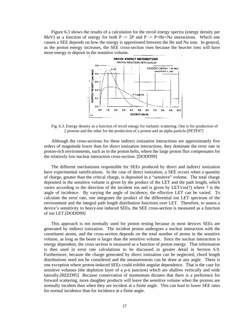
Figure 6.3 shows the results of a calculation for the recoil energy spectra (energy density perMeV) as a function of energy for both P -> 2P and P -> P+He+Na interactions. Which onecauses a SEE depends on how the energy is apportioned between the He and Na ions. In general,as the proton energy increases, the SEE cross-section rises because the heavier ions will havemore energy to deposit in the sensitive volume.
Fig. 6.3. Energy density as a function of recoil energy for inelastic scattering. One is for production of2 protons and the other for the production of a proton and an alpha particle.[PETE97]
Although the cross-sections for these indirect ionization interactions are approximately fiveorders of magnitude lower than for direct ionization interactions, they dominate the error rate inproton-rich environments, such as in the proton belts, where the large proton flux compensates forthe relatively low nuclear interaction cross-section. [DODD99]
The different mechanisms responsible for SEEs produced by direct and indirect ionizationhave experimental ramifications. In the case of direct ionization, a SEE occurs when a quantityof charge, greater than the critical charge, is deposited in a “sensitive” volume. The total chargedeposited in the sensitive volume is given by the product of the LET and the path length, whichvaries according to the direction of the incident ion and is given by LET/cos(?) where ? is theangle of incidence. By varying the angle of incidence, the effective LET can be varied. Tocalculate the error rate, one integrates the product of the differential ion LET spectrum of theenvironment and the integral path length distribution functions over LET. Therefore, to assess adevice’s sensitivity to heavy-ion induced SEEs, the SEE cross-section is measured as a functionof ion LET.[DODD99]
This approach is not normally used for proton testing because in most devices SEEs aregenerated by indirect ionization. The incident proton undergoes a nuclear interaction with theconstituent atoms, and the cross-section depends on the total number of atoms in the sensitivevolume, as long as the beam is larger than the sensitive volume. Since the nuclear interaction isenergy dependent, the cross section is measured as a function of proton energy. That informationis then used in error rate calculations to be discussed in greater detail in Section 6.9.Furthermore, because the charge generated by direct ionization can be neglected, chord lengthdistributions need not be considered and the measurements can be done at any angle. There isone exception where proton-induced SEEs could exhibit angular dependence. That is the case forsensitive volumes (the depletion layer of a p-n junction) which are shallow vertically and widelaterally.[REED95] Because conservation of momentum dictates that there is a preference forforward scattering, more daughter products will leave the sensitive volume when the protons arenormally incident than when they are incident at a finite angle. This can lead to lower SEE ratesfor normal incidence than for incidence at a finite angle.

28
The preceding description of proton-induced SEEs provides a basis for the followingsections. The tester should consider the following ?lessons learned? as they apply specifically toproton SEE testing.
6.2 Proton Beam Parameters.A careful selection of proton beam parameters is required to obtain valid data for predicting
SEE rates in space. These include proton energy, flux, and fluence.
6.2.1 Proton Energy.The selection of proton energy depends on what one wants to know about proton-inducedSEEs. If the goal is to screen parts for single-event latchup, the highest available energyshould be chosen and measurements need only be done at that energy. If the goal is to beable to predict SEU rates in space, it is necessary to measure the SEU cross-section as afunction of proton energy, from threshold to saturation. (The exception would be devicescontaining photodetectors where SEEs may be caused by direct ionization, and for whichother methods would have to be used.) The number of different energies needed depends onthe following:• Available accelerator time and the time to change proton energy (approximately an hour).• Budget to pay for accelerator time.• Maximum energy available from accelerator. Some accelerators have maximum proton
energies of 63 MeV, which may be too low for measuring saturation.• Accuracy of error-rate prediction. An accurate prediction of SEU rates in space depends
on how well the data can be fit with one of the standard functions describing thedependence of cross-section on proton energy. Section 6.8 will detail those functions.The dependence of SEU cross-section on energy for older devices was described by the1-parameter Bendel equation, which requires only one data point. However, the 1-parameter Bendel equation was found to be inaccurate for modern devices, and wasreplaced with a 2-parameter equation, which requires testing at a minimum of two protonenergies. One measurement should be done near threshold and the other near saturation.More recently, the Weibull equation and the error function have been used to fit the data.They have more adjustable parameters and so require more data points.
• The use of degraders to change beam energy raises the issue of straggle. Degraders areblocks of material through which the proton beam passes prior to striking the DUT. Asthey pass through the material, the protons lose energy by an amount that depends on theblock’s thickness and the material from which it is made. Section 5.14 discussed how tocalculate the proton energy loss using SRIM2000. The problem with using degraders isan effect called “straggle”, which is the spread in energy around the average energy of theproton beam after passing through a finite thickness of material. The energy loss isprobabilistic in nature, which is why the spread increases as the thickness of the degraderincreases. As long as the blocks are relatively thin and reduce the energy by only a smallamount, the straggle can be ignored, particularly at high energies where the cross-sectionis saturated. However, if thick degraders are used to reduce the average beam energy tothe threshold energy where the cross-section rises rapidly, straggle can lead to errors inthe measurement of cross-section. For example, a copper degrader available at IUCFused to reduce proton energy from 192.3 MeV to 59.6 MeV produces a spread in energyof 3.6 MeV(FWHM). A choice of degraders should be available at the acceleratorfacility.
• Measurements to determine the threshold are complicated by the fact that the cross-section is small and large proton fluences are required for good statistics. Large protonfluences can cause TID damage that will destroy the part well before measurements with

29
good statistics are obtained.(See section In this case it is advisable first to domeasurements at high proton energies and then at lower proton energies.
6.2.2 Proton Flux.The proton flux should be selected based on two factors: 1) the time required to reach aspecified fluence and 2) the expected error rate. Because of the significant cost involved forbeam time, all fluxes should be chosen with an eye toward saving beam time. However, toohigh a proton flux could lead to the system being overwhelmed and not operating properly.In the case of SEL, inaccurate values of fluence could occur due to the time lag betweenwhen an event occurs and when the beam is switched off. Good practice suggests that aninitial run be made, and the results used to adjust the flux for subsequent runs.
6.2.3 Proton Fluence.The fluence used for a test is determined by error statistics. If the number of single events isN then the error in the measurement is given by N0.5. For an error equal to 10%, N0.5/N mustbe equal to 1/10, which set N = 100. To satisfy this criterion, at least a hundred SEEs mustbe logged. (For a detailed discussion of statistical error, refer to an introductory book onstatistics.) This is sometimes not possible near the SEE threshold where the cross-section issmall and the device might be damaged as a result of proton-induced TID or DD before therequired number of SEE have been logged. (Although frequently ignored, plots of SEEcross-section versus energy should include error bars.) If there are no events, then themaximum fluence to test to is determined by the mission requirements. If the requirementsare not known, testing should stop either after a fluence of 1011 protons/cm2 or afterdestruction of the part, which ever comes first.
6.3 Whether to Test.Many attempts have been made to relate the LET threshold for SEUs induced by heavy ions
with the energy threshold for SEUs induced by protons.[ROLL90],[PETE92] In fact, a simpleequation has been developed:
Ab = L0.1 + 15where Ab is the A parameter in the Bendel 1-parameter equation and L0.1 is the LET value atwhich the cross-section is 1/10 of its saturated value. The Bendel Ab parameter is the protonenergy threshold for proton reactions that produce upsets. Evidently, parts that have very lowLET thresholds for ions will have proton thresholds around 15 MeV, and as the LET thresholdincreases so does the proton energy threshold. In theory, if the LET threshold has beendetermined, it is possible to use the above equation to obtain the upset rate from the Bendel Ab.In practice, however, this equation is based on a very crude approximation and should only beused as a rough guide and not as a justification for avoiding testing of one kind or another.
If a part has been tested with heavy ions and the threshold LET for SEUs found to besmaller than 15 MeV.cm2/mg, the part is very likely to be sensitive to SEUs generated by protons.Some parts exhibit great sensitivity to heavy ions, having LET thresholds lower than 15MeV.cm2/mg, yet they have been shown to be insensitive to protons. This has been observed forthe case of SEL. Nevertheless, if a part is suspected of being sensitive to SEL, it should be testedwith protons. Proton-induced SEL was first observed in 1992.[NICH92],[ADAM92]
6.4 Effect of PackagingBecause high-energy protons will penetrate the covers of most devices without losing much
energy, devices can be tested without having to remove the lid or plastic covering the part. Forexample, a 100 MeV proton has a penetration depth in aluminum of 3.7 cm. At low energies the

30
protons have a much smaller range. For example, the range of 20 MeV protons in an alloy such asiconel is less than 1 mm and the lid or plastic should be removed. The best approach is to useSRRIM2000 to calculate the range of protons with low energies in materials. If the energy loss issignificant, it is advisable to remove the packaging if possible, or get an accurate measure of thethickness and use SRIM2000 to calculate the energy loss.
6.5 Beam ControlAt UCD, control of the beam is passed on to the test engineer. To gain familiarity with the
software controlling the beam, one should try a few “dry runs” with no parts exposed. Also, toavoid accumulating fluence when the DUT is not operating, the DUT should be turned on andoperating properly before being exposed to the proton beam. For the same reason, the beamshould be turned off before the DUT at the completion of the test.
6.6 Special Concerns for Devices
6.6.1 SRAMs and DRAMs (Multiple-Bit Upsets)There is a possibility that high-energy protons will cause multiple-bit upsets (MBUs) inmodern SRAMs and DRAMs. MBUs were not observed during proton testing of oldermemories. MBUs are characterized by the fact that they occur simultaneously and areadjacent to each other. One possible cause of MBUs is the diffusion of charge away from theinteraction point. Another is that the proton could strike the control circuitry and cause linesof upsets. In either case, it is important to be able to distinguish MBUs from SEUs to obtainan accurate “event” rate. It is important to have a bit-map to determine the presence ofMBUs. Alternatively, one could use a low flux and do frequent reads of the device to seewhether more than one upset occurred and then analyze whether it was a MBU.
6.6.2 Optical DetectorsFor most devices it is not necessary to change the angle of incidence when doing protontesting. Optocouplers and photodetectors are the exceptions. Their cross-sections should bemeasured as a function of angle of incidence to determine whether direct ionization byprotons contributes. A large increase in the cross-section at high angles of incidence signifiesthe presence of SEEs caused by direct ionization.
6.6.3 Single Event TransientsAccurate SET testing is only possible if the same conditions are also used during testing asexpected in space. For example, SETs in optocouplers are affected by the output load, whichshould be identical to the actual output load used in the application. [REED98] Furthermore,the SET cross-section enhancement at grazing angle of incidence due to direct ionization byhigh-energy protons is much less than for low-energy protons because low-energy protonshave larger LETs. [REED98] The use of degraders that spread the proton energies should beavoided when looking for enhancement of the SET cross-section at grazing angle ofincidence because it makes it more difficult to identify whether direct ionization plays a role.Because the transients induced by protons are likely to be smaller in amplitude than thoseinduced by ions, it is important to make sure the trigger level of the detection equipment isproperly set. In addition, for later analysis of SET pulse height vs width, all transientscaptured on the oscilloscope should be stored.
6.6.4 Power MOSFETsSingle-event burnout in power MOSFETS has been studied in great detail.[TITU96] SEB istriggered in an “off” power MOSFET. Charge deposited either by heavy ions or by proton-

31
induced recoils turns on a parasitic bipolar transistor that sets up a current between the sourceand the drain. Regenerative feedback leads to a high current state that can burn out thedevice. SEBs observed in space have been attributed to heavy ions, but more recently,protons have also caused SEBs in regions where the radiation environment is dominated byprotons.[TITU98] Some parts seem to be more sensitive to proton-induced SEB while othersare more sensitive to heavy-ion induced SEB. Special procedures are required for SEBtesting in power MOSFETs, because once a device has exhibited burn-out it must bereplaced. This procedure requires more time and a large supply of parts. To prevent damage,a resistor is often added between drain and power supply to limit the maximum drain/sourcecurrent. This prevents the triggering of the high currents that lead to breakdown. Anotherpossibility is to us a power supply whose current can be switched off immediately it reaches ahigh value. Although most devices are run at de-rated voltages, which reduce the possibilityof SEBs, it is still necessary to find the voltages at which SEB is still a problem.
6.6.5 Stuck Bits in Memories (DRAMs and SRAMs)Stuck bits in memories have also been treated by Marshall [MARS99]. A stuck bit, alsocalled a hard error, is caused by the localized deposition of sufficient charge to produceinterface states that shift the threshold voltage sufficiently far that the device can no longerswitch. This is a localized TID effect. They were first observed in DRAMs in 1993[OLDH93] and the following year in a 1-Mbit SRAM [POIV94]. In the past, most stuck bitswere attributed to heavy ions. More recently, however, stuck bits have also been attributed toprotons. While testing memories for SEEs with protons, one should monitor both the stuckbits and the leakage current for total dose damage. Following the observation of excessiveleakage current or stuck bits, the part should be replaced because of TID damage.
6.6.6 Epitaxial Devices (including SOI) with Small DimensionsIn devices where the lateral dimensions are larger than the depth, the proton SEU cross-section may exhibit angular dependence, i.e. the cross-section increases with increasing angleof incidence.[REED95] The reason for this angular dependence is that the spallation reactionproducts are preferentially scattered in the forward direction. SOI devices may exhibit thiseffect. At normal incidence, the amount of collected charge is limited by the very thin siliconlayer and may not be sufficient to produce a SEU. However, at non-normal incidence, theforward-scattered daughter particles will travel a longer distance through the silicon beforereaching the underlying oxide layer. More deposited charge at finite angle means that theSEU cross-section is angular dependent and increases with increasing angle of incidence.
6.6.7 LatchupProtons are known to induce latchup in certain circuits, particularly those based on CMOStechnology. Therefore, when planning to test these types of devices, precautions should betaken to ensure that the device is not damaged due to latchup during testing. This can bedone by limiting the current with the use of resistors or by setting a limit on the maximumsupply current. Should a SEL occur, it would be necessary to cold reboot the system. If thisis necessary, the beam should be turned off immediately and kept off during the rebootingstage to avoid accumulating fluence when no test is being performed. Also, for latchuptesting the flux is usually kept very low to avoid the accumulation of dose between the timethe latchup is detected and the beam is turned off. Once the device is again operatingproperly, the beam can be turned back on. Therefore, the current to the DUT must bemonitored remotely and the rebooting accomplished either automatically or remotely. As thesupply voltage used for state-of-the-art devices is reduced, theoretical predictions show thatthe threat of latchup decreases. It is nevertheless prudent to test devices for SEL with protonsto confirm that they are latchup free.

32
6.6.8 Analog-to-Digital ConvertersTesting analog-to-digital converters (ADCs) is usually done in the quasi-static mode in whicha constant voltage is applied to the input and the digital output is monitored while the part isexposed to the beam. Because of inherent noise, it is usually necessary to mask off some ofthe least significant bits. The part is run with the beam off and bits are masked off until thereare no more SEUs. Most proton accelerators generate significant electrical noise that will addto the inherent noise. Therefore, the masking should not be done in the laboratory prior totraveling to the proton test facility. Instead, masking should take place once the part is inposition in front of the exit port, but with the beam block in place so there are no proton-induced SEUs. Many of the ADCs are manufactured using BICMOS technology in whichthe analog part is bipolar and the digital part is CMOS. If the CMOS part is not sensitive toproton-induced upsets and the bipolar part is, most of the SEUs will manifest themselves assmall deviations around the expected output, i.e., most of the upsets will be in the leastsignificant bits. It is therefore essential to minimize the noise while testing so that the effectson the least significant bits can be evaluated. In addition, advanced ADCs are very fast andwill not function well with long cables. Therefore, the testing equipment must be locatedclose to the ADC and should be shielded against damage by stray neutrons and protons.
6.7 Testing at SpeedElectronic devices such as logic circuits and opto-electronic devices such as a fiber optic data
bus must be tested at the same speed as that used in space because the error rate cross-section hasbeen shown to be frequency-dependent, i.e., the higher the speed, the greater is the error rate. Ifthe part is operated at a speed lower than intended, an underestimation of the error rate will result.Therefore, the bandwidth of the test setup should be commensurate with the test speed needs andthis precludes having the test equipment outside the vault. The test equipment must be placed inthe vault and controlled via an Ethernet or other system that allows remote control.
6.8 Number of Devices TestedThe number of DUTs of the same kind that can be tested will depend on many factors,
including their size (which determines how many can be tested at once), beam time available,budget and number of devices available. Frequently, one has to settle for testing a single devicebecause of cost or availability of parts. Generally, 2 devices from the same manufacturer and lotwould be acceptable for SEE testing, although 3 would be preferable. COTS devices, known tohave a large variability in threshold energies, certainly require testing of more than one part.
6.9 Data AnalysisProper data analysis is an important aspect of proton-induced SEE testing. Proton testing is
required for predicting SEE errors rates in space and involves the measurement of the proton-induced SEE cross-section as a function of energy. Two different theoretical approaches havebeen used to calculate the energy dependence. The first approach is to perform a Monte Carlocalculation (such as CUPID), which will not be discussed here. The second is a semi-empiricalapproach based on the energetics of nuclear interactions. There are three different equations thatone can use for fitting the data - the Bendel 1-parameter equation, the Bendel 2-parameterequation and the Weibull equation. The Bendel 1-parameter equation is not as accurate and is nolonger used, particularly if data is available at more than one proton energy.
6.9.1 Bendel 1-parameter EquationThe SEU rate was measured at a single energy and the value fit using the Bendel one-parameter function[BEND83], given by:

33
s = (24/A)14[1-exp(-0.18Y0.5)]4…………………………………..(1)
with Y=(18/A)0.5(E-A), and where E and A are in MeV. The cross-section is given in terms ofupsets per proton per cm2 per bit. If the SEU cross-section is to be measured at only a singleenergy, 60 MeV would be a good choice for a lightly shielded device, because there aregenerally as many protons in space with energies below 60 MeV as above.
6.9.2 Bendel 2-parameter EquationModifications to the Bendel one-parameter function involved using two fitting
parameters to obtain better agreement.[SHIM89] The resulting two-parameter function isgiven by:
s = S [1-exp(-0.18Y0.5)]4………………………………………(2)
where S is the proton limiting cross-section and Y is the same as in the 1-parameter Bendelequation. Figure 6.4 shows a comparison of 1-parameter and 2-parameter fits to data foractual devices.[PETE97] The curves have the same cross section at 60 MeV but a good fit tothe data is clearly obtained with only 1 curve. In general, it is better to use the 2-parameterrather than the 1-parameter equation.
Fig. 6.4. Results of attempts to fit the proton SEU data with both 1-parameter and 2-parameter Bendelcurves.
6.9.3 Weibull 4-parameter EquationThe integral Weibull function can also be used to fit the data and is given by:
s = s (8 )[1-exp(-((E-E0)/W)s]…………………….…………….(3)
where s (8 ) is the saturated cross-section, E0 is the threshold energy, W is the width of therising portion of the curve and S is the power that determines the shape. Because there arefour variables in the Weibull function, a minimum of four different energy measurementsmust be made, particularly in the vicinity of the threshold where the cross-sections tend to besmall. This approach is limited by the cost of beam time and the possibility of damaging theDUT when cross-sections are measured at energies close to threshold where a large fluence isrequired to obtain a few SEEs. However, it does provide a more accurate fit.

34
6.9.4 Proton EnergiesThe Bendell and Weibull functions all have the same basic shape – a smoothed out stepfunction that has a threshold at relatively low energy followed by a gradual rise to a saturatedvalue at high energies. For the most accurate predictions, it is necessary to obtain thecomplete shape of the SEE cross-section curve as a function of energy. However, the twomost important parameters are the threshold energy and the saturated cross-section. MostSEE cross-section curves resulting from proton testing are saturated at proton energies above100 MeV. This involves a single measurement at energy greater than 100 MeV. In contrast,it generally requires more than one measurement to determine the threshold. Forconfirmation that the measurements agree with the theory, cross-sections could be measuredat additional energies, but the actual number of energy values depends on budget andaccelerator availability
6.9.5 Check on results6.9.5.1 PROFIT
If heavy-ion SEU data is available, one can use PROFIT to check on theresults. [CALV96] The equation is:
s (p)sat = s (LET=15).c.Nat.s nuclear……………………..(4)
where s (p)sat is the saturated proton cross-section, s (LET=15) is the heavy-ioncross-section measured at LET = 15 MeV-cm2/mg, c is the charge collectiondepth, Nat is the number of Si atoms per cm3, and s nuclear is the average nuclearcross-section (6x10-26 cm2) for protons between 100 MeV and 200 MeV.However, the agreement is good in some cases and not so good in others, socare should be exercised when using this technique.
6.9.5.2 FIGURE OF MERITAnother check on whether the measured proton cross-section is reasonable is touse the Figure of Merit (FOM) [PETE96]. The FOM for heavy ions is givenby:
225.0L
FOM HLσ= …………………………………(5)
where s HL is the limiting heavy-ion cross-section per bit at large LET and L0.25
is the LET at 25% of the limiting cross-section. The FOM can also be obtainedfrom the limiting proton SEU cross-section sPL :
FOM = 4.5 x 10⁴xsPL……………………..(6)
A check to see whether s PL is reasonable can be done by calculating the FOM from equation (6)and comparing it with the FOM calculated from equation (5) using the heavy-ion data. A largedisagreement signals the possibility of an error in the one or both of the measurements.

35
7.0 TID Issues and Lessons LearnedThe basic message of this section is that using a proton beam to test for TID is rarely cost-
effective due to annealing, enhanced low dose rate effects and the need to test multiple devices.Most TID testing is accomplished with gamma rays in a 60Co cell. However, because TID effectsoften occur in conjunction with SEE and DDD, it is important to understand the mechanismsresponsible for TID so that in those cases where, for example, both SEE and TID need to bemeasured, they can be done simultaneously with protons.
7.1 BackgroundIn the previous section we discussed the effects of free-carrier generation in semiconductors.
In this section we will discuss free-carrier generation by ions in insulators, such as oxides used inintegrated circuits. The ions generate tracks of e-h pairs in insulators that can lead to devicedegradation or failure via TID. Many years of research devoted to the study of radiation effectsin the most common insulator SiO2 have resulted in a good understanding of the mechanismsinvolved. Not all aspects, however, are understood and the research continues apace. Previousshort courses at the annual Nuclear and Space Radiation Effects Conferences provide excellentand detailed discussions of TID effects. [FLEE95], [DRES98], [LERA99]
As already pointed out, proton beams are not the first choice for doing TID testing because ofcost, beam availability, and dose rate effects. Most radiation test engineers use X-rays from anX-ray generator or gamma rays in a Co60 cell to test for TID. Both X-rays and gamma rays arehigh-energy photons that produce radiation damage via ionization of the atoms making up theoxide. Even though photons are very different from protons, the concept of absorbed dose todescribe energy loss applies to both and depends on LET. In fact, data suggests that there is verylittle difference between a rad(SiO2) generated by protons or by photons.[PEAS01]
There are, however, differences in charge generation in Si and SiO2. One difference is theamount of energy needed to generate an e-h pair in Si (3.6 eV on average) compared with SiO2
(17 eV). Another difference is the much lower carrier mobilities in SiO2 compared with Si; theelectron mobility is 20 cm2V-1s-1 and hole mobilities range from 10-4 to 10-11 cm2V-1s-1, dependingon electric field and temperature. A model that has proved useful for describing hole mobility isthat of polaron hopping via the continuous random walk approximation.[MCLE76] In thepresence of an electric field, the electrons rapidly exit the oxide, while the holes move much moreslowly in the opposite direction, hopping from one site to another. The larger the electric fieldand the higher the temperature, the faster the holes move. For positive bias on the gate of aMOSFET, electrons in the insulator move towards the gate and holes move towards the interfacebetween the insulator and the semiconductor. Some of the holes become trapped in the vicinityof the interface where they form a layer of positive charge. The electrical characteristics oftransistors are altered by the presence of charge in the vicinity of the interface. As an example,trapped positive charge shifts the threshold voltage of MOS transistors. In addition, by a processthat is not completely clear, the holes also lead to the formation of interface traps that also affecttransistor performance through threshold voltage shift and majority carrier mobility degradation.

36
Fig. 7.1. Fractional yield of charge generated by various forms of radiation as a function of electricfield.[MCLE89]
Recombination of e-h pairs plays a big role in determining how much damage results from aspecific dose. The greater the recombination, the fewer holes remain to produce trapped chargeand interface states. Geminate recombination, in which the e-h pair recombines with itself,occurs for low e-h densities generated by low LET ions or gamma rays.[AUSM86] Columnarrecombination refers to electrons and holes recombining with other holes and electrons anddominates at high e-h densities generated by high LET ions.[JAFF13] Therefore, geminaterecombination will dominate for high-energy protons with low LETs and columnarrecombination will dominate for low energy protons with higher LETs. At intermediate LETs,both geminate and columnar recombination will contribute. Recombination is suppressed in thepresence of an electric field resulting in a larger fractional yield of carriers in the oxide. Fig. 7.1shows a large variation in the fractional yield of carriers for different kinds ofradiation.[MCLE89] For example, under an electric field of 2MV/cm, the fractional yield forexposure to 60Co gamma rays is over 90%, whereas that for 700 keV protons is about 25%. High-energy protons should have a higher fractional yield than low-energy protons.
The trapped positive charge gives rise to an electric field that shifts the transistor’s thresholdvoltage in the negative direction. For example, in an n-channel MOS transistor operating ininversion, the trapped holes tend to make it harder to turn the device off.[FLEE95] The holesalso produce interface states via processes that are not fully understood, but are known to dependon temperature, electric field, time and total dose. The interface states have energies that covermost of the semiconductor energy bandgap. Those above the Fermi level are acceptors and thosebelow are donors. Therefore, for both n- and p-channel MOS transistors, the absolute value ofthe threshold voltage increases after irradiation due to the creation of new interface states. TIDdamage may manifest itself as an increase in the leakage current, a change in the frequencyresponse, and, ultimately a total loss of functionality.
The magnitude of TID damage depends on exposure rate (proton flux) and elapsed timefollowing exposure. Such time-dependent effects occur because the holes move relatively slowlytowards the interface and, once trapped, they can be annealed out over time, especially at elevatedtemperatures. A detailed discussion of time dependent effects is beyond the scope of this reportand the interested reader is referred instead to a number of excellent articles that include

37
discussions of time-dependent effects.[DRES98], [MCLE89], [FLEE95] A brief description ofthe manifestations of dose-rate effects and annealing is in order.
One important time-dependent effect that poses problems for proton TID testing is known asenhanced low dose rate sensitivity (ELDRS) in which certain bipolar devices have been shown todegrade at much lower levels of TID if the dose rate is well below 1 rad(Si)/s, a dose rate moreakin to that in space.[NOWL92] Fig. 7.2 shows an example of how the level of damage dependson dose rate. To test a device to a TID level of 1 krad(Si) at a dose rate of 0.01 rads(Si)/s wouldrequire about 30 hours. Because of beam costs and availability and because of difficulties relatedto controlling a beam with such low flux, this is clearly not a practical method of doing low dose-rate testing. Therefore, proton beams should never be used for ELDRS testing.
Fig. 7.2. Relative damage as a function of dose rate for various linear devices.[JOHN94]
Fig. 7.3. Threshold voltage shift as a function of dose for different dose rates, illustrating how thedifferent time constants for trapped charge and interface state generation and anneal affect themagnitude of the threshold voltage shift.[WINO86]

38
Another dramatic example of a dose-rate effect that has been known for some time is “super-recovery” or “rebound”.[WINO86],[FLEE95] Super-recovery refers to the fact that, while theinitial trapped positive charge begins to decline due to annealing, the interface state densitycontinues to increase. As was previously pointed out, irradiation produces both trapped positivecharge and interface states. Fig 7.3 shows that at low dose rate, the threshold voltage shift ispositive and the part fails due to timing problems, whereas at high dose rates the part fails due toa negative threshold voltage shift that results in a large leakage current. The positive charge istrapped in a much shorter time than required for the buildup of interface states. In addition, thepositive charge can undergo annealing, whereas the interface states do not. Therefore, n-MOStransistors irradiated at high dose rates (>50 krad(Si)/s) will exhibit a buildup of positive chargethat shifts the threshold voltage in the negative direction leading to failure through excessivecurrent leakage. Over short time intervals, the buildup of interface states is negligible so they donot contribute. However, if the n-MOS device is irradiated at low dose rate (< 1 rad(Si)/s), thepositive charge has time to anneal, reducing the amount of negative voltage shift. At the sametime, the negative interface states have an opportunity to grow, causing a positive shift in thethreshold voltage. The combination of the two can lead to such a large positive shift that thedevice will fail through timing effects. Test Method 1019.5 addresses these issues by requiringhigh-temperature annealing following high dose-rate testing. Therefore, in principle, devices canbe tested for TID using proton beams if Test Method 1019.5 is followed. However, it is still anexpensive alternative to 60Co testing because of the need to test multiple parts, especially COTSparts that are known to have large variability in failure levels.
On occasion the test engineer wishes to test parts after incremental steps of TID to monitorhow the part’s functionality or other parameters change with dose. After each TID increment, theparts have to be tested and this can consume a great deal of time, adding significantly to the costof testing. In this case the advantage of using 60Co is clear.
Exposure of devices to proton beams produces both TID and DD damage. However,majority-carrier devices, such as those based on MOS technology, are not affected by DD.Therefore, it is not necessary to test MOS devices for TID damage using proton beams. Insteadthey should be TID tested using 60Co or X-ray sources. The only reason to consider TID testingat a proton accelerator is if it is done in conjunction with other measurements, such as during SEEor DD testing. For instance, testing a CMOS memory for SEUs with a proton beam will alsoresult in TID damage. After significant exposure, as would be the case in a SEU hard device, theTID damage may be so severe that the device exhibits increased leakage current, stuck bits, and,in the worst case, failure to operate. It is important to know the levels of TID damage when doingSEE testing because the TID damage can skew the SEE data.
Certain devices, such as optocouplers, degrade via both TID and DD with the DDcontribution overwhelming that of TID. Testing optocouplers with 60Co or X-rays alone willgrossly understate the damage levels because these two techniques do not generate significantDD. Therefore, optoelectronic devices that degrade via both TID and DD should be tested withproton beams for a more realistic assessment of their survival levels in a proton-dominatedenvironment.
7.2 Calculation of Total Ionizing DoseThe TID from protons can be calculated from the proton LET and the fluence by using the
following formula:
Dose(rads(SiO2)) = (LET(SiO2))•(Fluence)•(1.6E-05)……………………(7)

39
The LET, which has units of MeV-cm2/mg, is obtained from SRIM2000 with proton energy andSiO2 as inputs. The fluence (#/cm2) is obtained from the computer controlling the exposure. Asan example, a 60 MeV proton has a LET of 9x10⁻³ MeV-cm2/mg in SiO2 so that a TID of 100krads(Si) will require a fluence of approximately 7x10¹¹ particles/cm2. The accelerator at UCDproduces a beam with a diameter of 6 cm, which is equivalent to an area of approximately 27cm2. Using a beam current of 1 nA, the TID of 100 krad(Si) can be accumulated inapproximately 1 hour. Test Method 1019 specifies the dose rates required for doing TID testingto take into account effects such as “rebound.” Although Test Method 1019 only applies togamma ray testing, it can, nevertheless, be used as a guide for selecting the proton flux (dose rate)when doing TID testing with protons.
7.3 Factors Affecting TID DamageIdeally one would like a one-to-one correspondence between dose deposited and damage.
Factors that affect this one-to-one correspondence are the density of e-h pairs generated by theprotons (which depends on proton energy) and the magnitude of the electric field in the oxide.These two factors affect the rate of recombination, which ultimately determines the damage level.Therefore, the proper proton energy should be selected and the device should be under theappropriate bias during testing.
7.3.1 Proton EnergyThe choice of proton energy needed for TID testing depends on the space environment and onshielding. As pointed out in the introduction, the number of holes that survive long enough toreach the interface is affected by either geminate or columnar recombination. High-energyprotons have low LETs which lead to low-density charge tracks for which geminaterecombination dominates. Conversely, low-energy protons have relatively higher LETsproducing higher density tracks for which columnar recombination dominates. An additionalfactor suppressing columnar recombination is the electric field itself. Therefore, if there issufficient shielding to reduce the flux of electrons and low-energy protons, the particlespectrum seen by the DUT will be dominated by high-energy protons. This suggests that TIDtesting be done with high-energy protons (> 60 MeV). Furthermore, TID testing with protonsshould also be done under the proper operating biases because they affect the recombination.If the spacecraft does not provide much shielding, low-energy protons and electrons willdominate the environment seen by the DUT. This is a more complicated situation becauseelectrons produce low density tracks for which geminate recombination dominates, whereaslow-energy protons produce relatively higher density tracks for which columnarrecombination dominates. For the case where the electron flux exceeds the proton flux, high-energy protons may be used for TID testing. When the proton flux is greater, low-energyprotons should be used.
7.3.2 Testing Under BiasBecause bias is, in most cases, the condition that leads to the most severe TID degradation,proton testing should be done under the bias expected when the part operates in space. Fig.7.1 shows charge yield as a function of electric field. Evidently, the charge yield is greatlyreduced in the absence of bias suggesting that the parts should always be tested under bias.The most realistic conditions involve testing the part under the bias applied during normaloperation.
7.4 Selection of Proton FluxThe proton flux determines the dose rate. For the case of gamma irradiation, it is specified by
MIL Std 883 Test Method 1019. This test method suggests a range of dose rates from 50rads(Si)/s to 300 rads(Si)/s. Although test method 1019 does not include proton testing, it can be

40
used as a guide for selecting dose rate. The proton dose rate can be calculated using the equationgiven in Section 7.2. Accelerators have no difficulty supplying proton fluxes that give dose ratesin the range specified by Test Method 1019. The reason for not doing TID testing with protonsbecomes evident when post irradiation effects (PIE) are considered. As an example, considerTID testing for MOS devices. Test Method 1019 specifies that following irradiation, a roomtemperature anneal should be done until parametric values return to within specifications, but nolonger than the time the device will be exposed to radiation in space. This essentially means thatonly one exposure can be done and then the device must be returned to the test engineer’slaboratory for the annealing part which may take many weeks. Accelerated annealing is anotheroption and involves first exposing the devices to 1.5 times the intended application specificationand then heating it at 100 oC for 168 hours. This is clearly even less practical for testing at aremote proton accelerator. A greater difficulty arises when testing certain bipolar circuits forenhanced low dose rate sensitivity (ELDRS), which is not addressed in MIL STD 883 TestMethod 1019. For ELDRS, one needs dose-rates of around 0.01 rad(Si) per second. Such a lowdose-rate is not practical with a proton beam, because of beam time costs and availability. Veryhigh fluxes may distort the internal electric fields in the oxides due to the creation of charge thatscreens out the electric field. At sufficiently high fluxes, the DUTs temperature might rise dueproton energy absorption.
7.5 Estimate of TID Levels before Testing.A TID test usually involves a series of radiation exposures followed by measurements to
determine functionality or the value of some device parameter sensitive to TID. To decide onwhat dose increments to use requires a rough idea of the dose at which the device fails. Thenumber of increments is limited by the accelerator time available. As an example, if it issuspected that the device fails at 10 krad(Si), one might choose to test at the following TID levels:1 krad(Si), 2 krad(Si), 5 krad(Si) and 10 krad(Si). A totally different set of TID levels would beused if the part were known to have a failure level of 100 krad(Si). They might be 10 krad(Si), 20krad(Si), 50 krad(Si) and 100 krad(Si). Selecting the latter levels to test a device that actuallyfails at a TID level of 10 krad(Si) would not provide the necessary data. Obviously, it is notalways possible to know the DUT’s failure level ahead of testing. Sometime an educated guesscan be made based on known TID levels of similar parts in the same technology.
7.6 Monitoring TID DamageTID damage manifests itself as either a change in a particular operating parameter, such as
leakage current, or as a failure of the device to function. Therefore, if TID is expected to occurwhen testing for SEE, the proper device parameter must be monitored. A TID screening testusing gamma rays in a 60Co cell should be done before SEE testing to see whether it will survivethe expected TID levels. If it will not survive, then one can save a considerable amount of moneyby not doing any SEE testing.
7.7 Testing More than One DeviceIf the devices are much smaller than the beam diameter and more than one device needs to be
tested, it is recommended that more than one device at a time be positioned in the beam andtested. The size of the beam and the uniformity vary from one accelerator to another. This willlimit the number of samples that can be tested at a time.
7.8 Fluence and TIDIf the part being tested for SEE is not very sensitive and if the proton energy is near the
threshold, there are likely to be very few SEEs. Obtaining decent statistics requires a highfluence at relatively low proton energies which means the TID might limit the testing. However,the high fluences might cause TID failure. Consider a part that has a TID failure level of 10

41
krad(Si) when exposed to 30 MeV protons. For a fluence of 1 proton/cm2, the dose is 3x10⁻⁷
rads(Si). After a fluence of 3.0x10¹¹ particles per cm2, the device will fail. At 30 MeV, the cross-section might be quite small – on the order of 10-10 cm2. For good statistics at least 10 upsets areneeded, which means that we must expose the part to 1011 protons/cm2. This means that the doseis 3.0x10⁴ particles/cm2, which is 30 krad(Si) and many parts will fail before reaching that level.
7.9 Dose Modified by Shielding.To calculate how shielding modifies the absorbed dose, one can use the computer program
SHIELDOSE[SELT80] The program calculates the absorbed dose as a function of depth inaluminum shielding material of spacecraft, imparted by electrons and protons in orbit.SHIELDOSE calculates, for arbitrary proton and electron incident spectra, the dose absorbed insmall volumes of different detector materials for the following aluminum shield geometries:• a semi-infinite plane medium, as a function of depth; irradiation is from one side only,• at the transmission surface of a plane slab, as a function of slab thickness; irradiation is from
one side only.• at the centre of a solid sphere, as a function of sphere radius; irradiation is from all directions.
The program is part of SPENVIS (www.spenvis.oma.be/spenvis) and can be used for a firstapproximation of the absorbed dose. For doing more refined calculations in three dimensions, apowerful program is NOVICE.
42
8.0 Displacement Damage Dose TestingSo far, this monograph has dealt with two of the three types of radiation damage produced by
protons – SEE and TID. The third type involves the degradation of electric or opticalperformance as a result of proton-induced displacement damage (DD) that occurs in a wide rangeof devices, including bipolar transistors, light emitting diodes and photodetectors. Although DDoccurs everywhere in an integrated circuit, only DD in the semiconductor degrades. This differsfrom TID, which occurs in insulators used in the construction of transistors. Devices, suspectedof exhibiting DD sensitivity, should be tested for their level of sensitivity if they are to operate inproton-rich environments, such as in the belts around the earth.
8.1 BackgroundBoth SEE and TID damage in devices operating in space are caused by ions losing energy via
ionization of the material they pass through. Ions also lose energy via another mechanism - non-ionizing energy loss (NIEL) - a process whereby the incident ions collide both elastically andinelastically with atomic nuclei, knocking them out of their equilibrium positions in the process.The atomic nuclei initially displaced by the incident ions are called primary knock-on atoms(PKAs). The damage associated with displaced atoms in the semiconductor lattice is calleddisplacement damage (DD) and the equivalent dose is termed displacement damage dose (DDD),a concept that has not yet been widely accepted. Although less than 0.1% of the total energy lostby a proton is via NIEL, DD effects can cause significant performance changes in device such asoptocouplers, LEDs and CCDs. The reader is referred to the following three excellent reviewarticles on DD. [MARS99], [SUMM92], [SROU88]
The interstitials and vacancies, produced as a result of nuclear collisions, form Frenkel pairs.Most of them recombine within a very short time (~ 1 sec) and no permanent damage isproduced. A few of the Frenkel pairs escape recombination and form stable defects. Onecomponent of a Frenkel pair, the interstitial atom, is electrically inactive and has no effect ondevice performance, especially for very high energy (>100 MeV) irradiations. The othercomponent, the vacancy, may form many different types of electrically active complexes. Forexample, the vacancy may combine either another vacancy to produce a divacancy, or with adopant atom (phosphorus or oxygen) to form an electrically active defect. The defect densitydepends on the recoil energy of the PKA. At low recoil energy (< 2 keV), coulomb scatteringdominates and numerous isolated defects are produced. At high recoil energy the interactioncross-section is lower, but the defect structure is more complicated, taking the form of cascadesor tree-like structures that contribute a significant fraction of the total DD. [WOOD81].
The vacancy complexes are crystal lattice defects with energy levels (traps andgeneration/recombination centers) in the semiconductor bandgap. As such, they can have a majoreffect on device performance. The most important material parameters governing the operationof semiconductor devices are minority carrier lifetime (recombination lifetime), generationlifetime, majority carrier concentration and majority carrier mobility. [MARS99] Energy levelsin the semiconductor bandgap associated with DD are capable of affecting any one of thesematerial parameters. In general, the generation and recombination centers have an order ofmagnitude lower density than the majority carrier concentration. Therefore, the minority carrierlifetime, which depends on the density of generation and recombination centers, will be degradedwell before the carrier concentration. Since mobility degradation is not significant, except at veryhigh damage levels, DD will have the most effect on devices that depend on minority carrierlifetimes through generation and recombination. Minority-carrier lifetime degradation causesreductions in the gain of bipolar transistors, the responsivity of detectors and the efficiency ofsolar cells. Certain light sources, such as amphoterically doped LEDs, are greatly affected by DD,whereas others, such as lasers, are not. The reasons for these differences are not yet well

43
understood. DD has very little effect on MOS-based devices, in part because the operation ofMOS devices is governed by majority carriers rather than by minority carriers, and because of therelatively small amount of energy lost by NIEL compared with the amount lost by ionization.Therefore, TID effects will appear in MOS devices well before any effects due to DD.
Laboratory sources of radiation used for TID testing, such as X-ray generators and 60Co doproduce some DD, but they are generally not used for DD testing because they produce onlyrelatively small amounts of DD. Instead, DD testing is done with protons or neutrons. Protontesting is usually done at accelerators, such as cyclotrons, whereas neutron testing is done eitherat a reactor, such as the one at Aberdeen Arsenal, or at an accelerator, such as the one at LosAlamos National Laboratory. Neutrons are produced in an accelerator when high-energy protonscollide with heavy nuclei, such as lead, in thin foils placed in the proton beam. It has beendemonstrated experimentally that some devices, such as CCDs, optocouplers and solar cells,degrade via both DD and TID. Combined effects are usually tested with protons, which arecapable of producing both TID and DD, rather than neutrons, which produce primarily DD. Incases where it is necessary to study DD effects without the complications of TID, neutrons fromaccelerators are used. High-energy (>1MeV) electrons may also be used for generating DD.Although electrons, like protons, lose most of their energy via ionization, they do producedefects, albeit only isolated defects. To generate defect clusters, high-energy protons are needed.
The amount of DD produced by protons depends on their energy – the lower the protonenergy the greater is the DD density. Protons in space have a wide range of energies, whichrequires that the DD must be known for the whole range of proton energies if accurate predictionsof total DD are needed. To avoid having to measure DD over a wide range of proton energies,testing is done at a few energies and the full damage spectrum is obtained from NIELcalculations. Either analytical or Monte Carlo methods may be used to calculate NIEL. Theanalytical calculation is quite complicated and the interested reader is referred to the followingreferences.[BURK86],[LIND63] Large differences in energy loss rate for NIEL and forionization are shown in figure 8.1. The Monte Carlo programs for calculating NIEL are HETC,CUPID and SRIM. The reader is warned against using TRIM for calculating NIEL for protonswith energies greater than 8 MeV because TRIM includes only elastic (Coulombic) interactionsthat dominate for proton energies less than 8 MeV. At energies greater than 8 MeV inelasticprocesses dominate and these are not included in TRIM. Were TRIM to be used for calculatingNIEL for high-energy protons, an underestimation of the total DD would result. This underscoresthe importance of including the proton energy spectrum in calculations of NIEL. NIEL is to DDwhat LET is to SEE and TID, and even has the same units (keV•cm2/g).
The environment experienced by a device in space also has a neutron component producedwhen cosmic rays interact with matter, such as spacecraft shielding. The thicker the spacecraftshielding, the greater is the flux of secondary neutrons. For example, secondary neutrons mayconstitute a significant fraction (10%) of the proton fluence when the shielding consists of 0.2 cmthick tungsten. [JUN01] Neutrons are also produced when cosmic rays interact with nitrogenatoms in the earth’s atmosphere. Although they are capable of producing SEUs in densememories on board aircraft flying at high altitudes (60,000 feet) and high latitudes, their flux isnot sufficient to produce significant DD.[TABE93]

44
Fig. 8.1. Energy loss calculations for protons in silicon via both ionizing and non-ionizingmechanisms.[MARS99]
The next step after calculating NIEL is to make the connection between NIEL and deviceperformance degradation. Damage caused by NIEL can affect material parameters that aredependent on the density of generation/recombination centers. One such example would be thereduction in the diffusion length (L) with fluence (F ) according to the following equation:
1/L2 = 1/Lo2 +KF
The factor K denotes a “damage constant” that can be calculated if L, Lo and F are known.However, this is not very useful because material parameters cannot, in most cases, be measured.Instead, test engineers measure device or system parameters, such as bipolar transistor gain, solarcell efficiency or photodiode dark current. These parameters are measured as a function offluence, and most of them (but not all) are linearly dependent on fluence. For instance, thechange in the inverse of bipolar transistor gain is related to the fluence through a “damage factor”according to the following equation:
1/hFE = 1/hFE0 + K(E, particle type)F
Here, the factor K(E, particle type) is the particle and energy dependent displacement damagefactor, which is determined by measuring the transistor gain both before and after exposure to aproton fluence, F . This kind of equation holds for other device parameters, such as solar cellefficiency and dark current, and for different energies and particle types. (One exception is theempirical equation for solar cell power, which exhibits a logarithmic rather than simple lineardependence.)
The final step is to relate the damage factor (K(E, particle type)) to NIEL. It has been shownempirically that, for most devices, the damage factor depends linearly on NIEL, i.e.,
K(E, particle type) = C • NIEL(E, particle type)
This relationship is demonstrated empirically for the minority carrier lifetime in a bipolartransistor. Fig. 8.2 shows the minority carrier lifetime damage factor ratio as a function of protonenergy and particle type for a number of different transistors. K(E, particle type) is calculatedfrom the data for each transistor, energy and particle type. The data are normalized to thatcalculated for damage in Si induced by 1 MeV neutrons. Then NIEL calculations are carried out

45
and the results are also normalized to the NIEL for 1 MeV neutron-damage in Si. Fig. 8.2 showsthe data points in the energy range from 4 MeV to 200 MeV and for protons, deuterons andhelium ions. The calculated NIEL ratios for the energy and particle of interest normalized to 1MeV neutron-damage are shown as the solid lines. The figure shows that the data points matchwell with the calculations and no scaling factor is needed to relate the device performancedegradation to the NIEL. This comparison has been made for a number of different deviceparameters and, in most cases, exhibits a linear relationship.
Fig. 8.2. Dependence on proton energy of minority carrier lifetime damage factors andNIEL.[SUMM87]
It is essential, when performing NIEL calculations, to be aware of the following limitations:• In general, NIEL calculations for Si devices are fairly accurate, giving results within a
factor of two of the measured values. However, there are discrepancies at both low (<20eV) and high energies (>20 MeV) so that if NIEL is calculated at either the low or highenergy limits and the result scaled to all other energies, the total NIEL curve will besignificantly in error.
• NIEL calculations at very low proton energies (a few eV) close to the displacementdamage threshold in Si, are known to be inaccurate and measurements at those energiesshould be avoided. [DALE88] A complicating factor for low-energy protons is that theNIEL changes along the proton’s path as it slows down and comes to a stop.
• There are also discrepancies at high proton energies. Discrepancies between measureddamage factors and those calculated from NIEL have been noted in GaAsdevices.[BARR95] This area is currently under active investigation and promisingprogress has recently been reported, which should lead to more accurate NIELmeasurements for high-energy protons.[MESS01, WALT01].
• A questionable assumption affecting the calculation of NIEL is that the displacementdamage factor is always linearly dependent on NIEL. In some cases, the dependence hasbeen shown to be super-linear, with more damage at higher NIEL or lower protonenergy.[DALE89] Theories have been proposed to explain this effect. One theoryattributes the effect to the dependence of the PKA energy spectrum on proton energy andthe fact that Frenkel pairs produced by low-energy PKAs would have lowerrecombination rates, with a concomitant higher damage factor.[DALE93]

46
• Another assumption that does not always hold is the linearity between the degradation ofthe device parameter of interest and the fluence. This is clearly seen for devices such asoptocouplers where:
1/CTRf ? 1/CTRi +KF
CTRi is the initial current transfer ratio, defined as the detector current divided by theLED current, CTRf is the current transfer ratio after irradiation, and F is the fluence. Theanalysis of this case is more complicated because optocouplers consists of threecomponents, LEDs, photodetectors and coupling media, and the CTR depends on bothTID and DD. This is discussed in more detail in section 9.1.
The concept of “damage equivalent fluence” is frequently used when comparing DDproduced by any particle having any arbitrary energy. The concept refers to the fact that theparticle fluences required to produce a specific level of DD in a device for two different particleshaving different energies can be compared using NIEL. As a consequence, measurements of thedamage factor as a function of fluence for a particular particle at a single energy makes it possibleto predict the level of damage at any energy and for any other particle. This effectively limits therequired amount of accelerator testing, thereby saving money and time. This approach is basedon accurate knowledge of the energy dependence of NIEL, which is not always the case. Thereduced energy range limits the uncertainty in the NIEL calculations and requires carefulselection of proton test energy.
The differential proton fluence spectrum to which a shielded device is exposed in space is acontinuum in energy, the exact shape of which depends on the environment and on the shieldingmaterial and thickness. Instead of having to take data at a large number of different energies, dataat a few energies should suffice. Then, assuming that the damage factor depends linearly onNIEL, the change in a device parameter can be predicted for any particle fluence at any energy.By extension, the DD for a particular proton spectrum involving a continuum of energies can bedetermined. This information is needed for the calculation of the total DD in a device exposed toprotons with a broad energy spectrum.
8.2 Proton EnergyBecause of cost and time, proton DD testing should be done at only a few proton energies,
possibly just one or two energies. Selection of the optimum proton energy for DD testingdepends on the DUT’s anticipated environment, consisting of the natural radiation environmentmodified by shielding. Unshielded devices (e.g. solar cells) may experience a significant amountof DD from electrons and low-energy protons, whereas well-shielded devices will experiencerelatively more damage from high-energy protons (40-100 MeV). Although the damage, asmeasured by the electrical characteristics, may appear to be the same at high and low protonenergies, there are important differences in such factors as the rate of annealing that mandate amore careful selection of energy.

47
Fig. 8.3. Rate of energy loss in GaAs as a function of proton energy for both ionizing and NIEL.[MESS97]
One criterion suggested for selecting proton energy is based on the NIEL-weighted protonenergy spectrum, which is obtained by convoluting the calculated NIEL dependence on protonenergy with the proton energy spectrum modified by the proton’s passage throughshielding.[MARS99] Therefore, knowledge of both the NIEL dependence on energy and theshielded proton spectrum are needed. Fig. 8.3 shows the energy loss due to both ionizing andnon-ionizing (NIEL) interactions in GaAs. There is a very sharp onset of the NIEL curve at 200keV and a maximum at about 300 keV. By about 10 MeV, the rate of energy loss via DD isdown by more than three orders of magnitude. (The NIEL spectrum for protons in silicon isqualitatively similar.) The proton energy spectrum at the device depends not only on the locationof the spacecraft and on the time, i.e., whether the spacecraft is exposed to a solar proton event,but also on the degree of shielding. Heavily shielded devices will be exposed to relatively fewlow-energy protons and the displacement damage testing can be done at energies of around 50MeV, close to the NIEL weighted maximum. On the other hand, lightly shielded devices, likesolar cells, will be exposed to more low-energy protons and the maximum in the NIEL weightedproton spectrum will shift to lower energies.
Fig. 8.4 shows a comparison of the cumulative fraction of ionizing and displacement damagedose in GaAs as a function of slowed-down proton energy for a solar proton event such as that of19th October 1989.[MESS97] The figure clearly shows that a significant portion of the totaldisplacement damage for a lightly shielded device (3 mils SiO2) is from protons with energiesbelow 1 MeV, and that protons with energies greater than 10 MeV make very little contribution.As the thickness of the shielding increases, the curve moves to the right.

48
Fig. 8.4. Cumulative fraction of ionizing and NIEL dose as a function of slowed-down proton energy forGaAs covered with a 3 mil thick coverglass made of Si. [MESS97]
8.3 Measurement of Displacement Damage DoseIt is standard practice to measure the DD as a function of proton fluence and energy. At
present there is no formally accepted unit of displacement damage dose equivalent to therad(material) used for TID. There is also no dosimeter for measuring DDD. Instead, the fluenceand proton energy are recorded and may be used to calculate displacement damage dose. For thebest possible measurements of DDD, it is important to have accurate values of fluence and protonenergy.
8.4 Damage FactorThe choice of the proper damage factor to measure is important. For example, in the case of
DD in Si CCDs, one may consider reduction in charge transfer efficiency, increase in darkcurrent, or increased noise in the amplifier caused by DD. The choice can lead to differencesgreater than a factor of two in the predicted degradation level of a CCD.[DALE91]
8.5 Separation of DDD and TIDCertain devices such as optocouplers, are sensitive to both TID and DDD effects. The
prospect of qualifying the parts using a combination of 60Co gamma rays for TID and neutrons forDDD instead of protons presents itself. In practice it is not possible. First, accurate NIELcalculations have not been carried done for many materials of interest and there are alsoproblems, referred to in Section 8.1, with NIEL calculations at high proton energies in Si.Second, damage annealing greatly complicates the measurement. For instance, DD in lasers areannealed by charge injection, and TID effects in MOS devices are annealed by neutralization ofthe traps, particularly at elevated temperatures and positive gate bias. Therefore, using neutronsand gamma rays instead of protons to test for the combination of TID and DD should be avoided.
8.6 MicrodosimetryDD testing of modern devices is complicated by the fact that the devices have thin active
regions. Many of the PKAs produced as a result of protons colliding with nuclei at normalincidence will exit the sensitive volume and not contribute to the displacement damage. To avoidthe resulting erroneous prediction, the test can be done with protons incident from the back sidebecause those PKAs knocked out of the sensitive volume will be compensated for by PKAsgenerated outside the sensitive volume and knocked into it. Therefore, modern devices with verythin sensitive volumes should, if possible, be tested with protons incident from the rear and the

49
front and the relative amounts of damage compared to determine whether this effect does in factoccur.
8.7 Time After Exposure Before The Effects Of DD MeasuredIn most cases one can do the irradiation and then transport the devices back to the lab for
testing. For transport back to the laboratory, all the legs should be shorted together to preventbuildup of electric charge. Most of the vacancy-interstitial pairs recombine within less than asecond. The remaining recombination rate is much slower. This is not the case if one iscombining DD and TID effects. If significant annealing takes place after irradiation, this isprobably an indication that TID has made a major contribution. By including a room temperatureanneal, the effects of low dose rate in CMOS parts can be simulated, provided the part has notfailed.
8.8 Bias During ExposureWhen testing for DD, it is usually not necessary to bias the device during irradiation. Certain
devices, however, such LEDs undergo charge-injection annealing so they should be appropriatelybiased during exposure to the proton beam. The application conditions should be known and thedevices tested under the same conditions. However, if the proton testing includes both TID andDD, careful attention must be paid to applying the proper bias because the TID is very dependenton bias.
8.9 Number Of DevicesWhen testing devices such as Vertical Cavity Surface Emitting Lasers (VCSELs), the
variability in the response is so great that one should test on the order of ten devices for goodstatistics.[MARS99]
8.10 Presence Of Background NeutronsNeutrons are produced during proton testing at an accelerator. They can, in principle, add to
the DD, but in most cases the neutron flux is 10-4 times that of protons and so can safely beneglected [BERG97].
8.11 FluxFor most devices, the flux for DD testing is determined in large part by the total fluence
required to reach a desired level of damage and by the time (dollars) available for testing.Because most of the recombination of vacancy-interstitials takes place in less than a second, it isnot necessary to use low fluxes for which long exposure times would be required.
8.12 Shielding CalculationsThere are various programs that calculate the transport of radiation through material
including: BRYNTRN, FLUKA, HZETRN, GEANT4, SIREST(NASA Langley uses HZETRN)SHIELDOSE and NOVICE. CRÈME96 calculates a numerical solution to the one-dimensionalcontinuity equation, taking into account both ionization loss and nuclear fragmentation.Limitations to the transport code are 1) does not include neutron production in the shielding,which is important for thick shielding and devices that are sensitive to DD, 2) does not includetarget fragments, 3) can only use Al shielding material, 4) Si is the only target. NOVICE is themost versatile code because it gives the particle distributions following passage through shieldingmaterial.

50
9.0 Combined Effects TestingPrevious sections have covered the issues associated with testing for proton ionizing dose,
displacement damage, and single event effects. Often, a single test article may be sensitive toeffects from two or perhaps even all three of these mechanisms. In this section, we considercircumstances in which combined effects must be considered, and explore specific test cases withreferences and suggestions of how to proceed where it is either known or suspected thatcombined effects may complicate data collection or interpretation.
9.1 Discrete and Linear Bipolar TechnologiesDiscrete bipolar transistors may be sensitive to gain degradation from base current
leakage increases due to both bulk displacement damage induced introduction of generationcenters and also from ionizing dose induced surface states and their associated dark current. As anexample of the relative roles of these mechanisms, see the proton damage study reported bySummers, et al. (SUMM87). Their study measured proton energy dependent damage factors, withthe goal of using the damage factor as a metric to correlate the Non-ionizing Energy Loss (NIEL)in both n-type and p-type Si. By using 2N2222 NPN devices and 2N2907 PNP devices, bothmaterial systems were analyzed using the following relation:
1/hFE = 1/hFE0 + K(proton energy)F
Where 1/hFE0 is the pre-irradiation reciprocal gain, K is the damage factor, and F is theparticle fluence. As is discussed in that paper, the above relation only applies to displacementdamage, and the response is typically non-linear when proton dose is deposited on virgin devices.To avoid this complication, prior to proton testing, the ionization induced surface leakage effectswere examined as a function of collector current by exposing test samples to C0-60 gammaradiation. In doing so, it was demonstrated that the ionization component of the damage could betaken to saturation, and that the surface generated leakage current due to ionization was stableover a period of weeks. Consequently, to guarantee a “pure” response to only the displacementinduced bulk leakage effects, the test samples were exposed to from 1.5 to 3.0 Mrad of Co-60gamma dose before exposing them to protons. Obviously, virgin devices would exhibit acomplex nonlinear response not described by the above relation, and the relative sensitivity tobulk damage versus surface leakage will be dependent on the dose, dose rate, and operatingcollector current. These factors must be taken into account when devising a test plan and in thedata analysis phase so that a reliable (or worst case) estimate of performance in a radiationenvironment can be made.
The susceptibility of linear bipolar ICs varies over a wide range because of significantvariations in processing, device design and specific performance requirements [see MARS99section 3.3.1, and references therein]. In general, it has been found that devices that containsubstrate or lateral pnp transistors are most sensitive to displacement damage as a result ofdegradation of the minority carrier lifetime in the wide base regions (i.e., low fT, or gain-bandwidth product). Circuit level design also plays a large role. For example, the use of a lateralpnp transistor as a primary input transistor operating at low current levels would be expected toincrease the device vulnerability to degradation from displacement damage. A recent study byRax et al. provides another example of a design practice which results in proton sensitivity[Rax98]. Their test results present data on an operational amplifier that fails its specificationlimit at an equivalent ionization level that is only 60% of that observed during gamma irradiation[Rax98]. Field oxide effects are thought to be responsible for the ionization related degradation,but the comparison clearly points to the need to consider both ionization and displacement relatedproton effects. The authors found that the output stage of the circuit is asymmetrical; it sources upto 10 mA, but is only guaranteed to sink 1 mA. It relies on the gain of a single substrate pnp

51
transistor to sink current from an external load, making it quite susceptible to displacementdamage as a direct result of circuit design. In other linear bipolar devices, either ionization ordisplacement effects may dominate, and both Co-60 and proton testing is recommended if anunderstanding of their respective roles is needed.
9.2 OptocouplersOptocouplers are hybrid modules comprised of an LED optical source, a coupling
medium, and a detector that is sometimes followed by an amplifier stage. They provide the basicfunction of DC isolation between circuit blocks, and find widespread application on spacecraft.The primary performance metric is the current transfer ratio (CTR), which is the ratio of thephotodetector collector current to the LED forward (i.e., drive) current. There are many differentoptocoupler designs and applications (digital and linear), and the radiation response is highlydependent on both factors. As a result of on-orbit failures of these devices in military and civilianspacecraft, laboratory investigations have been performed that confirm the important role ofdisplacement damage in device degradation. The failure in the TOPEX/Poseidon mission wasdue to CTR degradation at equivalent TID levels of 10-20 krad(Si) where about 1/3 of the TIDwas contributed by protons [Rax96]. Investigations of the radiation response of currentoptocoupler technology include [Lisc93, John99, DOrd97, Reed98]. To date, optocouplers withamphoterically doped AlGaAs LEDs have displayed the highest sensitivity to proton damage, andmodern devices have proved significantly more susceptible than earlier generations [Rose82].
The radiation responses of optocouplers are complicated by several factors that have beenconsidered in the recent work cited, and continue to be investigated. First, the devices are hybridmodules that may exhibit large part to part variability. A given commercial hybrid may haveinternal components (such as LEDs) that cannot be traced and may from several sources. Second,the observed radiation induced degradation results from a combination of TID and displacementdamage mechanisms, and the relative importance depends on the optocoupler design andapplication. Also, the coupler may be a part of a larger hybrid such as a DC-DC converter, whichincludes other radiation sensitive components [Reed98]. Third, as described in the previoussection, limits in our current understanding of the energy dependence of the NIEL for III-V (andternary) materials do not permit accurate on-orbit performance predictions, thereby necessitatingsignificant radiation design margins. It is also worthwhile to note that little is known aboutpossible connections between reliability issues such as lifetime and temperature and radiation-induced degradation. Currently, these effects are assumed to be independent. However, we doknow that some optocouplers have exhibited a significant CTR temperature dependence, which isan important consideration since operation well above room temperature is not uncommon onspacecraft [Rax96].
The importance of proton testing to evaluate the on-orbit response of an optocoupler isclearly demonstrated in Figure 9.1 which shows greatly decreased CTR for proton as compared toCo-60 irradiation. Rax et al. disassembled two types of optocouplers to investigate the modes ofCTR degradation [Rax96]. They found that the CTR performance was primarily determined bythe response of the LED to displacement damage, and that the amphoterically doped AlGaAsLED was significantly more susceptible than the GaAlP LED. As is often the case, a higherperformance device fabricated with more pristine material is also more radiation sensitive (e.g.,CCDs, solar cells, etc.), and an engineering trade of initial performance versus the radiationsensitivity of the device on-orbit must be performed. Displacement damage also affected thephototransistors in each optocoupler studied by Rax et al., with the reduction in photoresponsebeing a more significant than gain degradation. Optocouplers that use a photodiode (as opposedto a phototransistor) have been observed to have the best performance to date [Reed98]. In

52
addition, the optical coupling medium can be affected by ionizing dose, and lose couplingefficiency in a manner that is time, temperature, and dose rate dependent.
Texas Instruments 4N49
0
0.1
0.2
0.3
0.4
0.5
0.6
0.7
0.8
0.9
1
0 20 40 60 80 100 120Total Ionizing Dose (krad(Si))
Nor
mili
zed
CT
R
195 MeV ProtonsCo-60
If=1.1mAVce=5.0V
Figure 9.1 Comparison of proton and gamma irradiations clearly demonstrates the importance of bothionizing dose and displacement damage in CTR degradation. Despite the large part to part variability in thepre-irradiation CTR values, similar radiation degradation is observed when the post-irradiation CTRs werenormalized to their initial values [Rax96]. After [Reed98].
Application specific laboratory testing is necessary in order to assess on-orbit CTRperformance. To begin, we note there is a distinct difference in the performance and electricalcharacteristics of general-purpose optocouplers, such as those evaluated in [Lisc93, Rax96,Reed98] and those used in linear applications, e.g., DC-DC converters. General-purpose devicesexhibit a wide range of CTR values guaranteed to be above a set minimum, whereas those inlinear applications have specified CTRs within a narrow range. These differences need to beconsidered in designing a laboratory evaluation to determine the suitability of such devices foruse in space [John99]. In all cases, a proton induced radiation response of an optocoupler willdepend on the LED drive current since it impacts the operating point of the phototransistor andtherefore, its radiation response. To a lesser extent, the relative contributions of ionizing dosedamage versus displacement damage will also depend on the operating conditions.
The importance of application specific testing has been demonstrated by Reed et al. in astudy that measured the impact of LED drive current, circuit loading, and the phototransistorcollector-emitter voltage (VCE) on the proton induced CTR degradation. The experimental set-upis illustrated in figure 9.2. A radiation induced degradation in the LED light output results in areduction in the collector current of the phototransistor. If the transistor is in saturation then thechange in collector current will be minimal and the CTR will be essentially the same. However,if the same device is operating in the active region, the CTR will be quite sensitive to changes inLED output power. Whether or not the transistor operates in saturation is dependent on the LEDdrive current and VCE, (which itself depends on the output load). Figure 9.2 illustrates the loaddependence of the CTR radiation response for an optocoupler operated with a forward current of4 mA. It also demonstrates that the common practice of testing at a fixed VCE of 5 V with no

53
circuit loading significantly over-predicts the CTR degradation, although such data can be usedfor worst case estimates. Data such as these suggest the mitigation of CTR degradation byoperation of the optocoupler at the highest drive current possible while minimizing VCE to obtainthe desired IC for the application [Reed98]. In this case the optocoupler is driven into saturation.However, the trade-off between reliability concerns for LED operation in this mode must beconsidered. Also, the forward current selected may impact the rate of defect annealing observedin some LEDs.
VI
DUT
RI RL
Vo
VCE
Figure 9.2 CTR measurement setup showing the input voltage and resistance (VI and RI), and outputvoltage (VO). Two independent power supplies are used to sweep VI and VO. Changes in VI alter the LEDdrive current. VCE is the difference between VO and the measured voltage drop across the load resistance(RL), which can be varied. After [Reed98].
0.0
0.5
1.0
1.5
2.0
2.5
3.0
3.5
0.0E+00 2.0E+10 4.0E+10 6.0E+10 8.0E+10 1.0E+11 1.2E+11
Fluence (p/cm2)
CT
R/C
TR
o o
r V
ce/V
ceo
Vce/Vceo load=1 kohmVce/Vceo load=2.7 ohmCTR/CTRo load=1 kohmCTR/CTRo Load=2.7 ohmCTR/CTRo no load Vce=5V
Figure 9.3 Plot of the normalized CTR (solid lines) and normalized VCE (dashed lines) for an optocoupleroperated with a forward current of 4 mA and irradiated with 195 MeV protons. In the case of the 2.7 Ωload (with VCE remaining at 0.3 V), the degradation is almost twice that observed for the 1 kΩ load wherethe degradation is mitigated by an increase in VCE. (Vo was set so that the initial VCE = 0.3 V for bothloads.) After [Reed98].

54
In some cases, laboratory testing has shown the CTR response is dominated bydisplacement damage to the internal LED. As always, it is important to select the optimal protontest energy (or energies) based on analysis of the shielded proton spectrum relevant to a specificapplication. The relative importance of displacement damage dose and TID may be assessed bycomparing proton and gamma measurements as indicated in figure 9.1. This figure also showsthat the CTR response is very nonlinear with proton fluence (or TID or displacement damagedose), so that a damage factor cannot be defined. Nevertheless, the CTR degradation can beplotted versus the equivalent mission fluence or displacement damage dose to assess the end oflife performance. (Note that, to first order, the proton testing of CTR degradation can also beconsidered to incorporate the performance loss from TID effects.) As noted in earlier, the NIELfunction for LED materials does not accurately reflect the device response so accurate predictionsare not presently possible. In the absence of CTR measurements as a function of proton energy,we have three choices for a function to describe the energy dependence: (1) a calculated NIELcurve, (2) an experimental displacement damage curve from the literature (e.g., the LED datafrom [Barr95]), and (3) a piecewise “manufactured” worse case damage function. It is hoped thatfurther research to permit a better understanding of the radiation performance of optocouplers andthe applicability of the NIEL energy dependence will result in more realistic worst case analysesto facilitate the device selection process. However, there will still remain a wide variationbetween optocoupler manufacturers concerning issues such as component procurement andcoupler design. These issues need to be reflected in the sample size chosen for a radiation test,and significant de-ratings may be necessary to reflect the large part-to-part variations observedfor some of these hybrid devices.
9.3 Sensors and Imaging ArraysSensor arrays are always subject to single event transients in detector elements and
readout circuitry. Also, CMOS devices such as CCDs, CIDs and Active Pixel Sensors canundergo changes in biases due to flatband voltage shifts in gate oxides. Displacement damage tothe photodetector can result in increased leakage currents from either bulk of surface defects. InCCDs displacement damage also introduces trapping centers causing loss in the charge transferefficiency. Furthermore, increases in leakage may influence the measured amount of chargetransfer degradation. While CIDs and Active Pixel Sensors may experience flatband voltageshifts and increased leakage currents, they do not suffer from charge transfer degradation. A verydetailed discussion of the mechanisms and issues surrounding proton testing and proton effects isprovided in [MARS99 and references therein], and portions of this overview are summarizedbelow.
Silicon optoelectronic sensing arrays (visible, UV and x-ray) have been developed for awide variety of scientific, commercial and military uses in space. They contain a matrix of up toseveral million photosensitive elements (or pixels) which generally operate by converting thephoto-generated charge to a voltage that is multiplexed to a small number of output amplifiers.Present charge coupled devices (CCDs) are available with picoampere dark currents and chargetransfer efficiencies (CTE) in excess of 0.999999 per pixel. During the development of thesesensors, their susceptibility to ionizing radiation effects has been characterized and hardeningsolutions have been successfully implemented in many cases. The most commonly used CCD forvisible and UV detection is the buried channel device which has a shallow n-type layer implantedbelow the surface to keep the stored signal charge away from the traps associated with the Si/SiO2
interface. Such CCDs may be hardened to TID effects either by the use of radiation hardenedoxides [Carb93], or by biasing the device so that the silicon surface is inverted so that theinterface traps are filled and dark current generation is suppressed. This can be achieved with anextra implantation to form a multiphase pinned device [Jane95], or by shuffling the charge back
55
and forth between gates within a pixel faster than the surface states can respond (so-called ditherclocking) [BURK91, HOPK92]. These techniques typically maintain performance up to ~10-20krad(Si), and at higher doses flatband voltage shifts can result in increased dark currents when theinterface beneath the gate oxide is no longer held in full inversion.
Bulk displacement damage effects often dominate the radiation response in state-of-the-art scientific imagers when operated in natural particle environments up to several krad(Si)[e.g., JANE91, HOLL91b]. The flatband shifts and dark current increases that occur for ionizingdose levels below 10-20 krads(Si) are often not serious, and can be overcome with minor changesin voltages and operating temperature. In contrast, significant CTE losses from displacementdamage induced trapping sites are observed for proton exposures of less than 1 krad(Si).Nevertheless, the degree of CTE loss that is tolerable is very application-dependent, and it is stillpossible for a device to ultimately fail as a result of either TID or displacement damage effects athigher exposure levels. It is important to verify that flatband shifts will not take a device out ofinversion prior to the expected mission dose, and also to ensure that the readout amplifiercircuitry is robust. A detailed description of proton effects in CCDs may be found in a recentreview article [HOPK96] and references therein. Displacement damage degrades CCDperformance by decreasing the CTE, increasing the average dark current, by introducingindividual pixels with very high dark currents (or “spikes”), and by increasing the noise of theoutput amplifier. An overview of each of these effects follows.
One of the most important performance parameters for a CCD is the CTE, which is thefraction of signal charge transferred from pixel to pixel during read out. Arrays with 1024 x 1024pixels (and larger) are routinely used today, and require very low trap densities in order to operatecorrectly. For example, to reduce signal loss to less than 10% for 1000 pixel-to-pixel transfers, aCTE of at least 0.9999/pixel is necessary. For a typical device with 50 µm3 pixel volumes, thiscorresponds to less than one radiation induced defect every ten pixels, which can easily beexceeded during a typical space mission [HOPK96]. If a signal charge is trapped by a protoninduced defect, and remains trapped for more than one clock cycle, it will be lost from the signalcharge packet. The trapped charge is eventually re-emitted into trailing pixels, and produces asmeared image. It is the interplay between the temperature dependent carrier emission andcapture dynamics of the radiation induced traps and the device readout scheme and clocking ratesthat determine the CTE behavior of an irradiated CCD [MOHS74].
To understand this interplay, we consider the readout procedure for a 2-dimensional CCDarray. Signal charge packets are stored in the depletion regions formed underneath a biased gateduring the integration period. Since the gate voltage determines the potential well capacityunderneath, the signal charge can be moved down the rows in the buried channel by theappropriate sequencing of the gate voltages as indicated in Figure 9.4. The charge is confinedlaterally to a single row by an implanted channel stop. After each “parallel” transfer of the chargefrom one pixel to the next, the charge packet is clocked out of the serial register as depicted inFigure 9.4, and the whole process repeated until the imager readout is complete. Unfortunately,the time to read out the serial register is long enough for signal charge to be trapped. The signalcharge can subsequently be re-emitted into a trailing pixel thereby degrading the CTE. Since thecarrier emission times depend exponentially on temperature, the CTE response of a 2-dimensional CCD array is a strongly temperature dependent. In contrast to the typical area array,the linear CCD with clocking speeds at 1 MHz or more is relatively immune to proton inducedCTE degradation. This is because the capture times for key radiation induced defect levels, suchas the E-center, are too long relative to the charge transfer rate for the traps to efficiently trapsignal charge. Further details of radiation induced CTE degradation are beyond the scope of this

56
course, but are described in detail in many papers, including [MOHS74, BANG91, DALE93,JANE95, HOPK96].
Unfortunately, efforts to harden CCDs to displacement damage have not been nearly assuccessful as TID hardening. However, displacement damage effects can be ameliorated usingseveral techniques. CTE loss can be somewhat reduced by substantial cooling (often to about –80°C), to mitigate the trapping effects of the E-center (and also minimize dark current). Asillustrated in Figure 9.5, background charge can dramatically impact the CTE loss by filling thetraps so that they do not interact with the signal charge packet. The magnitude of theimprovement depends on the signal size, and usually comes at the price of additional noise.Another CTE hardening technique employs an additional phosphorus implant to confine thesignal charge to a smaller volume (referred to as a notch or minichannel) so that fewer traps areencountered as the signal charge is read out. Notches may be useful for low signal levelapplications and some CCD operating conditions, but the efficacy of a notch may varyconsiderably between manufacturers (or even lots from a single source). Further informationconcerning mitigation techniques may be found in [HOPK96] and references therein.
Direction ofcharge transfer
oxide
p-epi layer
p-substrateburied
n-channelchannelstops
V1V3V2
V1V3
V2V1
Figure 9.4 Illustration of parallel charge transfer down a row of MOS capacitors. A 3 phase CCD ispictured, in which each pixel is composed of 3 electrodes for charge transfer. The signal charge travels inthe buried channel and is restricted to a single row by implanted channel stops.

57
Figure 9.5 The charge transfer inefficiency (CTI = 1-CTE) for a CCD exposed to a proton fluence of7.2x109 cm-2, corresponding to TID of 4 krad(Si). Both the CTI and the efficacy of a dark chargebackground in CTI reduction are a function of signal size. After [HOPK94b].
For most satellite programs these mitigation techniques are not sufficient, and one mustresort to shielding. Unfortunately, high energy protons are not easily shielded against. In fact,quite thick (a cm or more) of high atomic weight shielding (e.g., Ta or W alloys) may be used tominimize displacement damage to the CCD. However, for heavily shielded devices, thedisplacement damage caused by secondary particles produced in the shielding itself is significant,and in some cases dominant [DALE93]. (Incoming protons may interact with the atoms in theshield material causing nuclear reactions that produce secondary particles such as neutrons andprotons.)
The second major effect of proton induced displacement damage on CCDs is the increasein dark current as a result of carrier generation in the bulk depletion region of the pixel. (Thisassumes that the CCD or CID has a hardened oxide and/or else is run in inversion so that thesurface dark current is suppressed.) The average dark current increase is characterized by adamage factor defined as the change in dark current per unit proton fluence.
Although the increase in the mean dark current with proton irradiation is important, thedark current nonuniformity is generally the biggest concern for CCD applications in space. NIELis an average quantity just as stopping power (or LET) is an average quantity. For ionizationeffects, the departure from the average dose delivered in a uniform medium is small down todimensions measured in hundreds of cubic nanometers. This is not the case with NIEL. For Sidetector arrays (such as CIDs or CCDs), with pixels measured in the tens or hundreds of cubicmicrons, the displacement damage sustained by adjacent pixels can vary considerably eventhough the identical pixels are exposed to the same environment [MARS89]. This nonuniformityis inherent to the statistical nature of the collision kinematics producing the displacement damageand therefore cannot be hardened against.

58
4 x 10¹⁰/cm2
N = 1967 Ni = 1.8
1 x 10¹¹/cm2
N = 4918 Ni = 4.5 2 x 10¹¹/cm2
N = 9835 Ni = 9.0
Figure 9.6 CID dark current histograms after exposure to increasing proton fluences. As the number ofprimary interactions per pixel, N, increases the distribution approaches a gaussian distribution. The highenergy tail is produced by very infrequent but large nuclear reaction events. (Ni is the average number ofinelastic interactions per pixel.) After [MARS90].
Figure 9.6 illustrates the spread in the dark current increases in individual pixels for a SiCID damaged incrementally by 12 MeV protons. The increase over the pre-irradiation darkcurrent is determined for each pixel and the three histograms are formed from the 61,504 pixelpopulation following each exposure. The high dark current tail is produced from single-particleinelastic nuclear reactions that deposit large amounts of displacement damage energy within thepixel, but are rare enough that relatively few pixels are affected at low fluences. Marshall et al.[MARS89, MARS99 and references therein] have studied the statistics of dark currentfluctuations in detail and developed quantitative descriptions of the effect. As seen in Figure 9.6,the analytic predictions (solid lines) of the dark current distributions [MARS90] agree well withthe experimental results. At higher proton energies, where the primary recoil ranges approach thepixel dimensions, Monte Carlo techniques are required to model the dark current distributions[DALE94]. In some devices, the presence of even very small high electric field regions canresult in dark current distributions that are significantly more skewed than those seen in Figure9.6 [SROU89, MARS89, MARS90, DALE90, HOPK92]. Improved device design and areduction of the applied biases can greatly minimize the occurrence of these very high darkcurrent pixels.
The high dark current pixels (so-called spikes) have been observed by several groups in avariety of devices, and also have been noted to have an erratic time dependence [see MARS99and references therein]. Hopkins and Hopkinson showed that the dark current within a singlepixel not only fluctuates in time, but also switches between well-defined levels and has thecharacteristics of random telegraph noise [Hopk92, Hopk93, Hopk95]. This behavior isillustrated in Figure 9.7 for an EEV CCD irradiated by 10 MeV protons. This type of noise

59
represents a significant calibration problem for some applications, and this is characteristic ofdisplacement damage, but similar behavior may also be seen in the noise characteristics of CMOSdevices from ionization induced interface state traps.
Figure 9.7 After the proton irradiation of a CCD, some pixels show time fluctuations in the dark currentwith the appearance of random telegraph noise. These measurements were performed on an EEV imager at10°C. The mean time constants for the high and low states increased at lower temperatures. After[HOPK93].
Despite the extreme sensitivity of CCDs to displacement damage, they are usedsuccessfully in space for many applications. Instrument shielding, CCD cooling, careful selectionof device architecture and operating conditions, and signal processing all can be used to partiallymitigate the proton induced performance degradation. Other types of two-dimensional sensorarrays, such as photodiode arrays, p-channel CCDs [SPRA97] and active pixel sensor arraysshow promise for future use in severe space environments.
9.4 CMOS MicrocircuitsIn general, CMOS devices typically are relatively insensitive to displacement effects, but
can suffer from ionizing dose related gate and field oxide leakage paths as well as single eventeffects. Single event latch-up and several other categories of single event upset may all bepossible (e.g. SEU, SEFI, SET, etc,). Characterization of SEE effects must be done carefullysince both the functionality of the device and the amount of SEE sensitivity may be affected bythe level of oxide related damage. Examples of both increased and decreased SEU sensitivitywith increasing ionizing dose have been noted.
Co-60 is most often used for ionizing dose evaluations of CMOS devices as it isrelatively inexpensive. To first order, the response of a given device to ionizing dose should notdiffer significantly if the dose is deposited with protons versus Co-60, but in some cases this isnot strictly true [see MARS99 and references therein]. In situations where CMOS devices aremonitored in real time during to proton exposure, parametric changes may arise due to gate orfield oxide damage from ionization. If device supply currents are used as a metric to determine

60
device functionality, care must be takes to assure that device operation has not been effected byproton induced single event effects, since latchup or functional interrupt may also result in shiftsin device supply currents.
More often, the test objective is to determine the SEU characteristics of a CMOS deviceto protons, and the unwanted shifts due to ionizing damage to the oxides represent a complicationto the measurement of SEU sensitivity. Prior to conducting proton SEU testing, Co-60 basedtests or some other indication of the device ionizing dose hardness level should be used as a guideto determine the appropriate number of devices to test. In practice, it is best to carefully monitorthe device parametrics during SEU testing and avoid acquisition of data outside the limits ofacceptable performance. In addition, a carefully monitored test and appropriate test plan canreveal the dependence of the SEU behavior on the level of oxide damage due to ionization. Oftenthe cross sections for SEU will increase as the dose increases, and this may influence the relativesensitivity of the device for specific categories of errors (e.g. bit flips from 0 to 1 may be favoredover 1 to 0 –or vice versa- as the part is damaged.
Petersen has pointed out that the total dose sensitivity of a technology can place practicallimitations on the accurate determination of proton SEE cross sections [PETE97]. This can betrue for TID hardened parts where assurances of very low cross sections are needed, but it may bemuch more important for COTS or other unhardened devices for which the TID failure levelsmay be only a few krad(Si). If the TID failure level of a candidate component is on the order of~10 krad(Si), then testing on an individual DUT will be limited to that dose. If protons of ~60MeV are used, this corresponds to a device cross section of ~10-11 cm2. Smaller cross sectionscannot be measured with a single device, although they may be important, especially for hardfailures and disruptive soft error modes.
The accurate determination of SEE cross sections for important events can require testingof many devices to TID failure levels to get even poor SEE statistics. Such measures may berequired when the SEE may lead to catastrophic failure, when many copies of the same device arepresent on the same satellite, or when many copies of the same device are used in a constellationof identical satellites.
The NASA Hubble Space Telescope offers one such example with its 12 Gbit Solid StateRecorder (SSR). The SSR is based on DRAM technology and uses 1440 die with eachcontaining 16 Mbits. Details of the proton SEE response of the individual die are provided in[LABE98], along with a description of in-flight anomalies that indicated proton sensitivity. Priorto flight, testing had been performed with both heavy ions and protons and on flight lot die. Inthese tests, block errors were identified through heavy ion testing, and the LET threshold wasmeasured at about 5 MeVcm2/mg. With such a low threshold, protons might be also be expectedto cause block errors, but after 3 flight lot die were tested to proton fluences of ~ 3 x 10¹¹ (~30krad(Si)), the devices failed from TID without exhibiting the single event induced block error.
However, after launch, two block errors were noticed and correlated with the protonenvironment. To understand the source of these errors, further analysis pointed to the need foradditional proton testing with a larger sample size. After a second round of testing with a samplesize of 100 die, it was determined that protons could lead to the block error condition, and 9 suchevents were noted on the 100 die sample set. Calculations of the error cross section and expectedin-flight error rate showed good agreement with the anomaly rate. Fortunately, for the HST casethe block errors were easily corrected with robust Reed-Solomon EDAC protection. The detailsof this example and others are found in [LABE98].

61
If the error condition were not easily corrected, or worse, if permanent failure resulted,the condition would not have been predicted with a small test sample set. When large numbers ofa given device are flown either on the same spacecraft or across a large number of satellites,correspondingly large samples sizes must be used to assess all possible SEE modes. The exactnumber will be a function of both the orbit and the TID response of the DUT. If hard failuremodes are possible, then large sample sizes may be warranted, even if only one device is to beflown.
9.5 GaAs and other High Speed DevicesHigh-speed technologies represent a special set of challenges for proton testing. A large
body of evidence has shown that GaAs, InP, SiGe, Si bipolar (ECL) and other high bandwidthtechnologies can exhibit sensitivity to proton induced single event effects, and in addition thelevel of sensitivity may be a function of the clock or data rate through the device [MARS99 andreferences therein, REED00]. Since these technologies are not based in CMOS, they are typicallynot sensitive to parametric failure from total ionizing dose below the 100 krad(Si) range. In fact,GaAs and other III-V devices may show little or no effects to Co-60 ionization levels in excess of1 Mrad(Si). Even so, care must be taken when measuring the SEU sensitivity to protons, andparametric shifts do not always provide insights into important changes in the response of thedevice under test.
In [MARS95], measurements of the proton SEU cross section in GaAs HIGFET deviceswere taken out to levels of greater than 50 Mrad(Si) without noting any parametric shifts ordegradation in the part performance. However, significant changes were noted in the SEU crosssection, which dropped by over 2 orders of magnitude. The authors explained the result in termsof displacement damage induced changes in the carrier lifetime in the GaAs semi-insulatingsubstrate. By suppressing the carrier lifetime, the charge collection leading to the SEUmechanism was also significantly suppressed, though without affecting device performance.These results suggested that the purposeful introduction of damage with high proton fluencesmight be used as a means of achieving some degree of SEU tolerance in an otherwise SEU softdevice. Here, we note the importance of assuring that the process of measuring the SEUsensitivity does not affect the results, and that many virgin parts may be needed if high fluencesare necessary to gain meaningful statistics on the SEU performance, even if the parametric shiftsare minimal.
9.6 Hybrids, Board, and Box Level Testing with Mixed TechnologiesIn hybrid, board level, or box level testing, the variations in technologies may result in a
variation in dominate degradation mechanisms from one part to the next. In such cases, test andmeasurement plans need to be devised carefully so that the most sensitive failure mode can bediscovered.
As an example of mixed technology testing, we will consider the case of protonevaluation of a commercial single board computer based on the Power PC-750® processor andmanufactured by DY-4, Inc. ®, and this board is shown in front of the UC Davis beamline inFigure 9.8. The SVME-179 board was not irradiated as an entirety during any single exposure,and due to the size of the board this would not have even been possible. Rather, the board areacontaining active components was divided into smaller regions that were carefully selected andirradiated individually using a collimated proton beam. Three sizes of beam collimators wereused for precise irradiation. A list of 25 regions covering all the active components on the boardwas prioritized according to likelihood of SEL or Total Ionizing Dose (TID) failure and the
62
importance of gaining information on that/those parts in order to maximize the data in the eventof DUT failure before the test ended.
Throughout the course of the series of tests, all regions were irradiated to a cumulativeproton fluence of 4 x 10¹⁰ protons/cm2 at 63 MeV, which corresponds to an ionizing dose of 5.6krad(Si). This corresponds to approximately 10x the expected mission fluence based on theintended application. Rather than expose individual parts to this level in the first pass, an initialtest round exposed each collimated region to a fluence level of 8.0 x 10⁹ protons/cm2 at 63 MeV,which corresponds to an ionizing dose of 1.08 krad(Si). This corresponded to approximately 2xthe expected mission fluence, and the initial test fluence reflected the need to show that themission needs would be met (for a very benign environment), along with the expectation that thiswould not exceed the failure levels for the commercial CMOS technologies represented in the~120 parts on the 2-sided board. Upon successful completion of this first pass, two additionalpasses were conducted with incremental fluences of 1.2 x 10¹⁰ protons/cm2 at 63 MeV and 2.0 x10¹⁰ protons/cm2 at 63 MeV. These later two passes of each exposure region were conducted togain statistics on SEU events and provide additional confidence in the ability of the board to meetthe intended application, but without exposing any single part to a high fluence before some datawere collected on all parts.
The overlay of the apertures with the board is shown as Figure 9.9 which also shows howthe exposures were grouped into three aperture sizes. Note that the overlay includes both thefront-side, backside, and mezzanine board positions, since at 63 MeV negligible attenuationresults from penetration of the populated base and daughter boards.
The consideration for a commercial single board computer for satellite applications is notconsidered without the acknowledgement of some risk of failure. The testing described here doesnot qualify the board for flight, however is an important step in understanding the risks.Knowledge gained through identification of failure and failure level of a specific part might beused to select an alternate supplier for that part, and improve the chances for mission success.The key point here is that careful selection of exposure levels and the sequence of exposures,including aperture sequence and size, are necessary in planning testing of complex test articleswith mixed technologies and unknown failure modes.
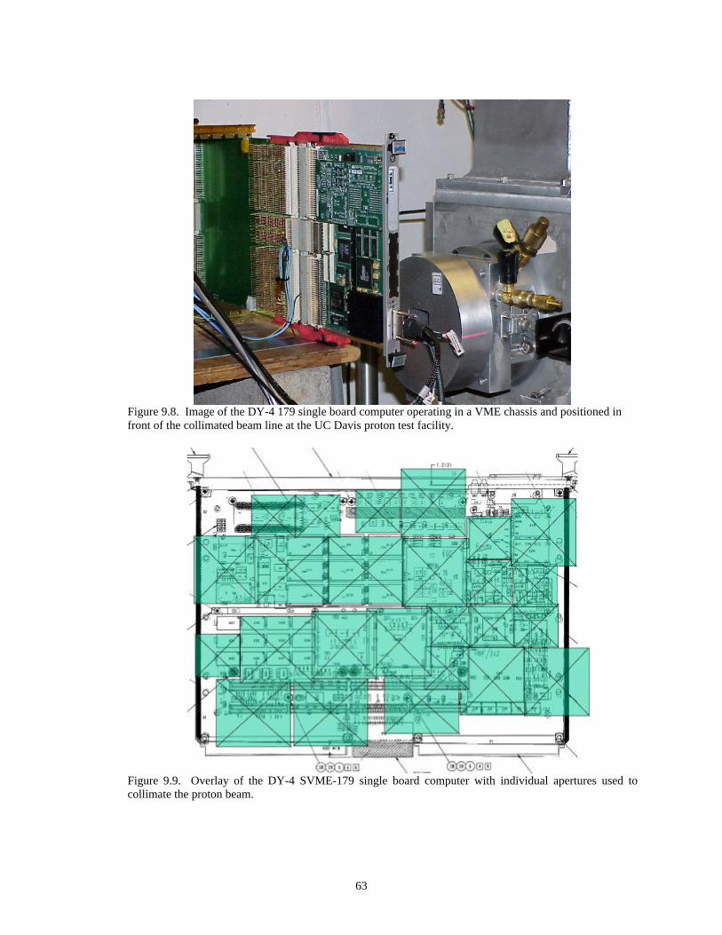
63
Figure 9.8. Image of the DY-4 179 single board computer operating in a VME chassis and positioned infront of the collimated beam line at the UC Davis proton test facility.
Figure 9.9. Overlay of the DY-4 SVME-179 single board computer with individual apertures used tocollimate the proton beam.

64
10.0 SummaryOur consideration of the practical aspects of proton testing has spanned a range of topics
from the availability of various facilities and their contact information, to the basic concerns fordosimetry, the associated radiation safety issues, and the complex response of varioustechnologies to proton damage. Based on lessons we have learned (in many cases the hard way)our summary of the special needs of testing with protons has emphasized the requirement forplanning and conducting testing in an environment where one particle leads to three criticaldevice failure mechanisms. Considerations for ionization damage, single event effects, anddisplacement effects are all important when planning proton tests, and in some cases devices maybe subject to two or three of these mechanisms. Further, the microdosimetry of proton damagecan be another important consideration when planning tests and the facility and energy at whichthe testing will be realized.
In presenting the issues associated with proton testing, we have attempted to providereferences to the literature and examples where proton testing is necessary to understand thedegradation modes and assuring mission success. The technical papers cited here provideessential insights into the basic mechanisms and test approaches needed to conduct testing thatallows quantification of the effects in a manner that can be related to the space environment. Inour case studies, we have selected topics that are recurring in our endeavors to assure success forNASA missions, and point out the nuisances of the end-to-end experience of planning the test,executing the test, and acquiring the data in a manner that can be analyzed to understanddegradation modes and predict the performance on enabling technologies destined to fly withprotons. Happy testing!
11.0 AcknowledgementsThe authors would like to thank the following individuals who contributed to the preparation
of this document:• Ray Ladbury for insightful and helpful suggestions.• Scott Messenger (Naval Research Laboratory) for reviewing the section on displacement
damage.• Alan Johnston whose tutorial on displacement damage testing at the Space Parts Working
Group Meeting in January 2002 provided some material on combined DD and TIDeffects.
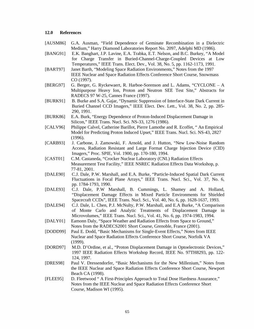
65
12.0 References
[AUSM86] G.A. Ausman, “Field Dependence of Geminate Recombination in a DielectricMedium,” Harry Diamond Laboratories Report No. 2097, Adelphi MD (1986).
[BANG91] E.K. Banghart, J.P. Lavine, E.A. Trabka, E.T. Nelson, and B.C. Burkey, “A Modelfor Charge Transfer in Buried-Channel-Charge-Coupled Devices at LowTemperatures,” IEEE Trans. Elect. Dev., Vol. 38, No. 5, pp. 1162-1173, 1991.
[BART97] Janet Barth, “Modeling Space Radiation Environments,” Notes from the 1997IEEE Nuclear and Space Radiation Effects Conference Short Course, SnowmassCO (1997).
[BERG97] G. Berger, G. Ryckewaert, R. Harboe-Sorenson and L. Adams, “CYCLONE – AMultipurpose Heavy Ion, Proton and Neutron SEE Test Site,” Abstracts forRADECS 97 W-25, Cannes France (1997).
[BURK91] B. Burke and S.A. Gajar, “Dynamic Suppression of Interface-State Dark Current inBuried Channel CCD Imagers,” IEEE Elect. Dev. Lett., Vol. 38, No. 2, pp. 285-290, 1991.
[BURK86] E.A. Burk, “Energy Dependence of Proton-Induced Displacement Damage inSilicon,” IEEE Trans. Nucl. Sci. NS-33, 1276 (1986).
[CALV96] Philippe Calvel, Catherine Barillot, Pierre Lamothe and R. Ecoffet, “ An EmpiricalModel for Predicting Proton Induced Upset,” IEEE Trans. Nucl. Sci. NS-43, 2827(1996).
[CARB93] J. Carbone, J. Zamowski, F. Arnold, and J. Hutton, “New Low-Noise RandomAccess, Radiation Resistant and Large Format Charge Injection Device (CID)Imagers,” Proc. SPIE, Vol. 1900, pp. 170-180, 1994.
[CAST01] C.M. Castaneda, “Crocker Nuclear Laboratory (CNL) Radiation EffectsMeasurement Test Facility,” IEEE NSREC Radiation Effects Data Workshop, p.77-81, 2001.
[DALE90] C.J. Dale, P.W. Marshall, and E.A. Burke, “Particle-Induced Spatial Dark CurrentFluctuations in Focal Plane Arrays,” IEEE Trans. Nucl. Sci., Vol. 37, No. 6,pp. 1784-1793, 1990.
[DALE93] C.J. Dale, P.W Marshall, B. Cummings, L. Shamey and A. Holland,“Displacement Damage Effects in Mixed Particle Environments for ShieldedSpacecraft CCDs”, IEEE Trans. Nucl. Sci., Vol. 40, No. 6, pp. 1628-1637, 1993.
[DALE94] C.J. Dale, L. Chen, P.J. McNulty, P.W. Marshall, and E.A Burke, “A Comparisonof Monte Carlo and Analytic Treatments of Displacement Damage inMicrovolumes,” IEEE Trans. Nucl. Sci., Vol. 41, No. 6, pp. 1974-1983, 1994.
[DALY01] Eamonn Daly, “Space Weather and Radiation Effects from Space to Ground,”Notes from the RADECS2001 Short Course, Grenoble, France (2001).
[DODD99] Paul E. Dodd, “Basic Mechanisms for Single-Event Effects,” Notes from IEEENuclear and Space Radiation Effects Conference Short Course, Norfolk VA(1999).
[DORD97] M.D. D’Ordine, et al., “Proton Displacement Damage in Optoelectronic Devices,”1997 IEEE Radiation Effects Workshop Record, IEEE No. 97TH8293, pp. 122-124, 1997.
[DRES98] Paul V. Dressendorfer, “Basic Mechanisms for the New Millenium,” Notes fromthe IEEE Nuclear and Space Radiation Effects Conference Short Course, NewportBeach CA (1998).
[FLEE95] D. Fleetwood “ A First-Principles Approach to Total Dose Hardness Assurance,”Notes from the IEEE Nuclear and Space Radiation Effects Conference ShortCourse, Madison WI (1995).

66
[GARR93] Henry Garrett, “Radiation Environments within Satellites,” Notes from the 1993IEEE Nuclear and Space Radiation Effects Conference Short Course, SnowbirdUT, (1993).
[HOLL91b] A. Holland, A. Holmes-Seidle, B. Johlander, and L. Adams, “Techniques forMinimizing Space Proton Damage in Scientific Charge Coupled Devices,” Trans.Nucl. Sci., Vol. 38, No. 6, pp. 1663-1670, 1991.
[HOPK92] G.R. Hopkinson, “Cobalt-60 and Proton Radiation Effects on Large Format, 2-D,CCD Arrays for an Earth Imaging Application,” IEEE Trans. Nucl. Sci., Vol. 39,No. 6, pp. 2018-2025, 1992.
[HOPK93] I.H. Hopkins and G.R. Hopkinson, “Random Telegraph Signals from Proton-Irradiated CCDs,” IEEE Trans. Nucl. Sci., Vol. 40, No. 6, pp. 1567-1574, 1993.
[HOPK95] I.H. Hopkins and G.R. Hopkinson, “Further Measurements of Random TelegraphSignals in Proton-Irradiated CCDs,” IEEE Trans. Nucl. Sci., Vol. 42, No. 6,pp. 2074-2081, 1995.
[HOPK96] G.R. Hopkinson, C.J. Dale, and P.W. Marshall, “Proton Effects in Charge-CoupledDevices,” IEEE Trans. Nucl. Sci., Vol. 43, No. 2, pp. 614-627, 1996.
[JAFF13] G. Jaffe, “Zur Theorie der Ionisation in Kolonnen,” Ann. Phys. (Leipzig) 42, 303(1913).
[JANE95] J. Janesick, T. Elliott, R. Winzenread, J. Pinter, and R. Dyck, “Sandbox CCDs,”Proc. SPIE, Vol. 2415, pp. 2-42, 1995.
[JOHN94] A.H. Johnston, G.M Swift and B.G. Rax, “Total Dose Effects in ConventionalBipolar Transistors and Linear Integrated Circuits,” IEEE Trans. Nucl. Sci. NS-41,2427 (1994).
[JOHN96] A.H. Johnston, “The Influence of VLSI Technology Evolution on Radiation-Induced Latchup in Space Systems,” IEEE Trans. Nucl. Sci. NS-43 505 (1996).
[JOHN99] A. H. Johnston and B.G. Rax, "Proton Damage in Linear and DigitalOptocouplers," to be presented at RADECS99 and published in the proceedings.
[JONE99] A. Z. Jones, C.D. Bloch, E.R. Hall, R. Hashemain, S. B. Klein, B. von Przewoski,K. M. Murray, and C.C. Foster, "Comparison of Indiana University CyclotronFacility Faraday Cup Proton Dosimetry with Radiochromic Films, a Calorimeter,and a Calibrated Ion Chamber, IEEE Trans. Nucl. Sci. NS-46, 1762 (1999).
[JORD97] T.M. Jordan, “Report No. EMPC 97.01.02.01,” NOVICE: A RadiationTransport/Shielding Code: Users Guide, Jan. 1997.
[JUN01] Insoo Jun “Effects of Secondary Particles on the Total Dose and the DisplacementDamage in Space Proton Environments,” IEEE Trans. Nucl. Sci. NS-48, 162(2001).
[JUN01A] Insoo Jun and William McAlpine, “Displacement Damage in Silicon due toSecondary Neutrons, Pions, Deuterons, and Alphas from Proton Interactions withMaterials,” IEEE Trans. Nucl Sci. NS-48, (2001).
[KOGA89] R. Koga and W.A. Kolasinski, “Heavy ion induced snapback in CMOS devices,”IEEE Trans. Nucl. Sci. NS-36, 2367 (1989).
[KOGA93] R. Koga, S.D. Pinkerton, S.C. Moss, S. LaLumondiere, S.J. Hansel, K.B. Crawfordand W.R. Crain, “Observation of single event upsets in analog microcircuits,”IEEE Trans. Nucl. Sci. NS-40, 1838 (1993).
[KNOL89] G.F. Knoll, Radiation Detection and Measurement, 2nd Ed., p. 216-226, p. 251-260,John Wiley and Sons, (1989).
[LABE98] K.A. LaBel, P.W. Marshall, J.L. Barth, R.B. Katz, R.A. Reed, H.W. Leidecker,H.S. Kim, and C.J. Marshall, “Anatomy of an Anomaly: Investigation of ProtonInduced SEE Test Results for Stacked IBM DRAMs,” IEEE Trans. Nucl. Sci.,Vol. 45, No. 6, pp. 2898-2903, 1998.

67
[LERA99] Jean-Luc Leray, “Total Dose Effects: Modeling for Present and Future,” Notesfrom the IEEE Nuclear and Space Radiation Effects Conference Short Course,Norfolk VA (1999).
[LIND63] J. Lindhard, V. Nielsen, M Scharff and P. Thomsen, “Integral Equations GoverningRadiation Effects (Notes on Atomic Collisions III),” Mat. Fys. Medd. Dan. Vid.Selsk., Vol. 33, 1 (1963).
[LISC93] H. Lischka, H. Henschel, O. Kohn, W. Lennartz, and H.U. Schmidt, “RadiationEffects in Light Emitting Diodes, Laser Diodes, Photodiodes, and Optocouplers,”RADECS93, IEEE Doc. No. 93TH0616-3, pp. 226-231, 1993.
[MARS89] P. W. Marshall, C. J. Dale, E. A. Burke, G. P. Summers, and G.E. Bender,“Displacement Damage Extremes in Silicon Depletion Regions,” IEEE Trans.Nucl. Sci., Vol. 36, No. 6, pp. 1831-1839, 1989.
[MARS90] P.W. Marshall, C.J. Dale, E.A. Burke, “Proton-Induced Displacement DamageDistributions and Extremes in Silicon Microvolumes,” IEEE Trans. Nucl. Sci.,Vol. 37, No. 6, pp. 1776-1783, 1990.
[MARS95] Paul W. Marshall, Cheryl J. Dale, Todd R. Weatherford, Michael La Macchia, andKenneth A. LaBel, “Particle-Induced Mitigation of SEU Sensitivity in High DataRate GaAs HIGFET Technologies,” IEEE Trans. Nucl. Sci. NS-42 1844, (1995).
[MARS99] Paul W. Marshall and Cheryl J. Marshall, “Proton Effects and Test Issues forSatellite Designers,” Notes from the IEEE Nuclear and Space Radiation EffectsConference Short Course, Norfolk VA (1999).
[MASS93] L.W. Massengill, “SEU Modeling and Prediction Techniques,” Notes from IEEENuclear and Space Radiation Effects Conference Short Course, Snowbird UT,(1993).
[MCLE89] F.B. McLean, H.E. Boesch and T.R. Oldham, “Electron-Hole Generation,Transport, and Trapping,” in Ionizing Radiation Effects in MOS Devices &Circuits,” Ed. By T.P. Ma and P.V. Dressendorfer, John Wiley and Sons, (1989).
[MESS97] S. R. Messenger, M.A. Xapsos, E.A. Burke, R.J. Walters, and G.P Summers,“Proton Displacement and Ionizing Dose for Shielded Devices in Space,” IEEETrans. Nucl. Sci. NS-44, 2169 (1997).
[MESS01] Scott R. Messenger, Robert J. Walters, Edward A. Burke, Geoffrey P. Summersand Michael A. Xapsos, "NIEL and Damage Correlations for High Energy Protonsin Gallium Arsenide Devices,” IEEE Trans. Nucl. Sci. NS-48 (2001).
[MOHS74] A.M. Mohsen and M.F. Tompsett, “The Effects of Bulk Traps on the Performanceof Bulk Channel Charge-Coupled Devices,” IEEE Trans. Elect. Dev., Vol. 21, No.11, pp. 701-711, 1974.
[NOWL92] R.N. Nowlin, E.N. Enlow, R.D. Schrimpf and W.E. Combs, “Trends in the TotalDose Response of Modern Bipolar Transistors,” IEEE Trans. Nucl. Sci. NS-39,2026 (1992).
[OLDH93] T. Oldham, K.W. Bennett, J. Beaucour, T. Carriere, C. Poivey and P. Garnier,“Total Dose Failures in Advanced Electronics from Single Ions,” IEEE Trans.Nucl. Sci. NS-40, 1820 (1993).
[PEAS01] R.L Pease, M. Simons and P.W. Marshall, “Comparison of pMOSFET Total DoseResponse for C0-60 Gammas and High-Energy Protons,” IEEE Trans. Nucl. Sci.NS-48, 908 (2001).
[PETE96] Edward L. Petersen, “Approaches to Proton Single-Event Rate Calculations,” IEEETrans. Nucl. Sci. NS-43, 496 (1996).
[PETE97] Edward L. Petersen, “Single Event Analysis and Prediction,” Notes from IEEENuclear and Space Radiation Effects Conference Short Course, Snowmass CO(1997).

68
[POIV94] C. Poivey, T. Carriere, J. Beaucour and T. Oldham. “Characterization of SingleHard Errors (SHE) in 1 M-bit SRAMs from Single Ion,” IEEE Trans. Nucl. Sci.NS-41, 2235 (1994).
[RAX96] B.G. Rax, C.I. Lee, A.H. Johnston, and C.E. Barnes, “Total Dose and ProtonDamage in Optocouplers,” IEEE Trans. Nucl. Sci., Vol. 43, No. 6, pp. 3167-3173,1996.
[RAX98] B.G. Rax, A.H. Johnston, and C.I. Lee, “Proton Damage Effects in LinearIntegrated Circuits,” IEEE Trans. Nucl. Sci., Vol. 45, No. 6, pp. 2632-2637, 1998.
[ROSE82] B.H. Rose and C.E. Barnes, “Proton Damage Effects on Light Emitting Devices,”J. Appl. Phys., Vol. 53, No. 3, pp. 1772-1780, 1982.
[REED95] R.A. Reed and P.J. McNulty, “Effects of Geometry on the Proton SEU Dependenceon the Angle of Incidence,” IEEE Trans. Nucl. Sci. NS-42, 1803 (1995).
[REED98] R.A. Reed, P.W. Marshall, A.H. Johnston, J.L. Barth, C.J. Marshall, K.A. LaBel,M. D’Ordine, H.S. Kim, and M.A. Carts, “Emerging Optocoupler Issues withEnergetic Particle-Induced Transients and Permanent Radiation Degradation,”IEEE Trans. Nucl. Sci., Vol. 45, No. 6, pp. 2833-2841, 1998.
[REED00] Robert A. Reed and Ray Ladbury, “Performance Characterization of DigitalOptical Data Transfer Systems,” Notes from the IEEE Nuclear and SpaceRadiation Effects Conference Short Course, Reno, NV (2000).
[SAWY76] Donald M. Sawyer and James I. Vette, “AP-8 Trapped Proton Environment forSolar Maximum and Solar Minimum,” National Science Center Data ReportNSSDC/WDC-A-R&S 76-06, (1976).
[SEXT92] F.W. Sexton, “Measurement of Single Event Phenomena in Devices and ICs,” Notefrom IEEE Nuclear and Space Radiation Effects Conference Short Course, NewOrleans, LA (1992).
[SPRA97] J.P. Spratt, B.C. Passenheim, and R.E. Leadon, “The Effects of Nuclear Radiationon P-Channel CCD Imagers,” 1997 IEEE Radiation Effects Workshop Record,IEEE No. 97TH8293, pp. 116-121, 1997.
[SROU88] J.R. Srour, “Displacement Damage Effects in Electronic Materials, Devices, andIntegrated Circuits,” Notes from IEEE Nuclear and Space Radiation EffectsConference Short Course, Portland OR (1988).
[SROU89] J.R. Srour and R.A. Hartman, “Enhanced Displacement Damage Effectiveness inIrradiated Silicon Devices,” IEEE Trans. Nucl. Sci., Vol. 36, No. 6, pp. 1825-1830,1989.
[SUMM87] G.P. Summers, C.J. Dale, E.A. Burke, E.A. Wolicki, P.W. Marshall and M.A.Gehlhausen, “Correlation of Particle-Induced Displacement Damage in Silicon,”IEEE Trans. Nucl. Sci. NS-34, 1134 (1987).
[SUMM92] G.P. Summers, “Displacement Damage: Mechanisms and Measurements,” Notesfrom IEEE Nuclear and Radiation Effects Conference Short Course, New OrleansLA (1992).
[TITU96] J.L. Titus and C.F. Wheatley, “Experimental Studies of Single-Event Gate Ruptureand Burnout in Vertical Power MOSFET’s,” IEEE Trans. Nucl. Sci. NS-43, 533(1996).
[TITU98] J.L. Titus and C.F. Wheatley, “Proton-Induced Dielectric Breakdown on PowerMOSFETs,” IEEE Trans. Nucl. Sci. NS-45, 2891 (1990).
[WALT01] Robert J. Walters, Scott R. Messenger, Geoffrey P. Summers, Edward A. Burke,Shyam M. Khanna, Diego Estan, S. Erhardt, Hui Chun Liu, Mae Gao, MargeretBuchanan, Anthony J. SpringThorpe, Alain Houdayer and Cosmo Carlone,“Correlation of Proton Radiation Damage in InGaAs/GaAs Quantum Well LightEmitting Diodes,” IEEE Trans. Nucl. Sci. NS-48 (2001).
69
[WINO86] P.S. Winokur, F.W. Sexton, J.R. Schwank, D.M. Fleetwood, P.V. Dressendorfer,T.F. Wrobel and D.C. Turpin, “Total-Dose Radiation and Annealing Studies:Implications for Hardness Assurance Testing,” IEEE Trans. Nucl. Sci. NS-33, 1343(1986).
[WOOD81] S. Wood, N.J. Doyle, J.A. Spitznagel, W.J. Choyke, R.M. More, J.N. McGruer andR.B. Irwin, “Simulation of Radiation Damage in Solids,” IEEE Trans. Nucl. Sci.NS-28, 4107 (1981).
[ZIEG96] J.F. Ziegler, J.P Biersack and U Littmark, “The Stopping and Range of Ions inMatter,” Pergamon Press, New York (1996).