Embed Size (px)
Citation preview

i
Protocol Framework Design for CC2510
Based Data-Gathering Sensor Network
SI SI
Technology and Communication
2011

1
VAASAN AMMATTIKORKEAKOULU
UNIVERSITY OF APPLIED SCIENCES
Degree Programme of Information Technology
ABSTRACT
Author SI SI
Title Protocol Framework Design for CC2510-Based Data-
Gathering Sensor Network
Year 2011
Language English
Pages 42
Name of Supervisor GAO CHAO
The objective of this project is to build up a demo system by using MCU. This
project consist one SINK node which broadcasts a SYNC frame to the sensor
node periodically. After receives a SYNC frame, the sensor node will send data
frame back to SINK node.
This project work is divided into 2 parts: SYNC and DATA Structure design and
embedded system programming.
My responsibility is to design SYNCE/DATA frame structure and build up the
demo system which defined in paragraph 1. All the works are implemented by
IAR Embedded System Workbench and the programming part is written by C
language.
Thesis report divided to 6 parts: introduce my project; explain background which
will be used in project; theoretical background chapter will explain more details
about information I used; analysis and description at approach and implementa-
tion chapter; last two chapters are summary and conclusion.

2
CONTENTS
ABSTRACT ............................................................................................................ 2
LIST OF ABBREVIATIONS ................................................................................. 3
TABLE OF CONTENTS ........................................................................................ 4
1 INTRODUCTION ............................................................................................ 8
2 BACKGROUND AND PURPOSE .................................................................. 9
2.1 Embedded System ..................................................................................... 9
2.2 Wireless Sensor Network .......................................................................... 9
2.3 Low-cost & low power sensor .................................................................. 9
2.4 CC2510 Development Kits ..................................................................... 10
2.5 Development environment ...................................................................... 10
2.6 Purpose of project ................................................................................... 12
3 THEORTICAL BACKGROUND .................................................................. 13
3.1 SYNC&SINK protocol ........................................................................... 13
3.2 Access testing environment .................................................................... 13
3.3 Architecture............................................................................................. 14
3.4 Pin and I/O port configuration ................................................................ 15
4 APPROACH AND IMPLEMENTATION .................................................... 17
4.1 Hardware Setup ....................................................................................... 17
4.2 IAR Embedded Workbench Setup .......................................................... 18
4.2.1 Create a new project .................................................................... 18
4.2.2 General Options, Code Model..................................................... 20
4.2.3 Include source files ..................................................................... 23
4.2.4 Compile and Link ........................................................................ 23
4.3 TI SmartRF Programmer ........................................................................ 24
4.4 TI SmartRF Studio .................................................................................. 25
4.5 TI SmartRF sniffer .................................................................................. 29
4.6 Timer ....................................................................................................... 30
4.6.1 Timer activity .............................................................................. 30
4.6.2 Timer code .................................................................................. 31

3
4.6.3 Example of output compare mode in free-running mode ........... 33
4.7 SYNC structure ....................................................................................... 36
4.8 DATA structure ...................................................................................... 38
5 OUTCOME OF PROJECT ............................................................................ 41
6 CONCLUSIONS AND DISCUSSION .......................................................... 42
REFERENCES ...................................................................................................... 43
4
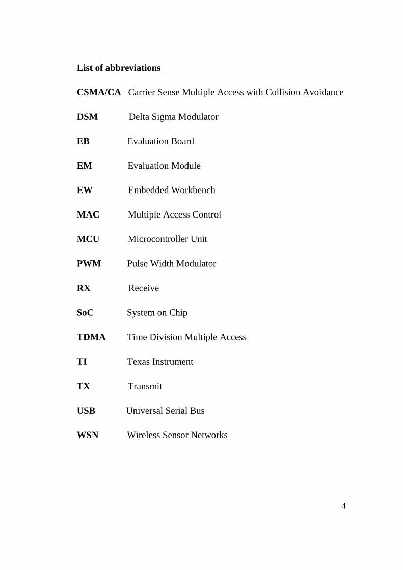
List of abbreviations
CSMA/CA Carrier Sense Multiple Access with Collision Avoidance
DSM Delta Sigma Modulator
EB Evaluation Board
EM Evaluation Module
EW Embedded Workbench
MAC Multiple Access Control
MCU Microcontroller Unit
PWM Pulse Width Modulator
RX Receive
SoC System on Chip
TDMA Time Division Multiple Access
TI Texas Instrument
TX Transmit
USB Universal Serial Bus
WSN Wireless Sensor Networks
5
LIST OF FIGURES, TABLES AND CODES
Figure 1 .................................................................................................................. 11
Figure 2 .................................................................................................................. 12
Figure 3 .................................................................................................................. 14
Figure 4 .................................................................................................................. 15
Figure 5 .................................................................................................................. 17
Figure 6 .................................................................................................................. 18
Figure 7 .................................................................................................................. 19
Figure 8 .................................................................................................................. 19
Figure 9 .................................................................................................................. 20
Figure 10 ................................................................................................................ 21
Figure 11 ................................................................................................................ 22
Figure 12 ................................................................................................................ 22
Figure 13 ................................................................................................................ 23
Figure 14 ................................................................................................................ 23
Figure 15 ................................................................................................................ 24
Figure 16 ................................................................................................................ 24
Figure 17 ................................................................................................................ 25
Figure 18 ................................................................................................................ 26
Figure 19 ................................................................................................................ 27
6
Figure 20 ................................................................................................................ 28
Figure 21 ................................................................................................................ 28
Figure 22 ................................................................................................................ 29
Figure 23 ................................................................................................................ 30
Figure 24 ................................................................................................................ 33
Figure 25 ................................................................................................................ 35
Figure 26 ................................................................................................................ 36
Figure 27 ................................................................................................................ 36
Figure 28 ................................................................................................................ 38
Figure 29 ................................................................................................................ 38
Table 1 .................................................................................................................... 16
Table 1 .................................................................................................................... 31
Code 1 .................................................................................................................... 32
Code 2 .................................................................................................................... 32
Code 3 .................................................................................................................... 34
Code 4 .................................................................................................................... 34
Code 5 .................................................................................................................... 37
Code 6 .................................................................................................................... 38

7
Code 7 .................................................................................................................... 39
Code 8 .................................................................................................................... 40

8
1 INTRODUCTION
With the extensive application of wireless communications, using of MCU (mi-
crocontroller units) wireless communications technology becomes more popular.
By developing of MEMS (Micro-Electro-Mechanism System), SOC (System-on-
Chip), wireless communication and low-power embedded system, there comes out
a new technology - WSN (Wireless Sensor Network), which has low-power, low
cost, distributed and self-organization characteristics.
SYNC2SINK is a global synchronization protocol designed for WSN (Wireless
Sensor Networks) [1]. It was built on a platform using CSMA/CA (Carrier Sense
Multiple Access with Collision Avoidance) protocol.
In this project, SYNC2SINK is the way that after in-group node receive SYNC
frame which broadcast from SINK node, it will sends DATA frame back. Every
period will process 5000ms, each of SYNC and DATA frame’s length is 13bytes
include Length, Destination Address, and Source Address, Transaction ID, Appli-
cation PAYLOAD and User Port parts.
The demo system composed of Chipcon SmartRF04 EBs (Embedded Board), and
three of CC2510 EMs (Evaluation Module). One of CC2510EM will be SINK
part which transmits the SYNC frame; one of CC2510EM will be set as receiver
mode. After received SYNC frame from SINK, it will change to transmitter mode,
send DATA frame back to SINK; the last CC2510EM will be the sniffer to moni-
toring the process of communication.
To implement SYNC2SINK protocol in our system, transmitter and receiver
mode, system clock, SYNC and DATA frame need to initialize in my program.
I will illustrate tools we used in this project at Theoretical Background Chapter,
and explain the process to build this demo system at approach and implementation
Chapter.

9
2 BACKGROUND AND PURPOSE
2.1 Embedded System
An embedded system is a single-purpose computer built into a larger system for
the purposes of controlling and monitoring the system. A general purpose com-
puter (e.g. a personal computer) is defined not to be an embedded system.
Examples: cell phones, DSTV decoders, MP3 players, ABS breaking systems, and
satellite guidance avionics. [2]
2.2 Wireless Sensor Network
WSN is a kind of a multi-hop Ad hoc network composed by lots of cheap micro-
sensor nodes which deployed in the monitoring region-hop Ad hoc network [3].
The aim of WSN is to perceive collaboration, collection and processing coverage
area perceived objects, send observers. Sensors, sensing object and observer con-
stitute the wireless sensor network.
WSN have many types of sensors, these sensors can detect a lot of information
including earthquakes, electromagnetic, temperature, humidity, noise levels, light-
ing intensity, pressure, and soil composition, size of movement object, speed and
direction of a wide variety of phenomena in the ambient conditions.
2.3 Low-cost & low power sensor
Low-cost sensor nodes are composed of a single chip with embedded memory,
processor, and transceiver which thanks for hardware technology improvement.
Base on low power capacities, sensor networks must include a large number of
sensor nodes because limited coverage and communication range. It is hard to re-
charge or replace the exhausted battery with wireless sensor network, so maxi-
mum node/network’s work time is most important. [4]
10
2.4 CC2510 Development Kits
The CC2510 is a true low-cost 2.4 GHz system-on-chip (SoC) designed for low
power wireless application. It combines the excellent performance of the state-of-
the art RF transceiver CC2500 with an industry-standard enhanced 8051 MCU, up
to 32kB of in-system programmable flash memory and 4kB of RAM, and many
other powerful features.
CC2510 is designed to offer wireless communications at 2.4GHz, with a bit rate
up to 500kBaud. CC2510 has a highly integrated 8051-compatible microcontroller
and up to 32kB of in-system programmable flash memory. [5]
2.5 Development environment
2 computers installed windowsXP operating system, at least 2GB free space hard
disk, a serial port, 2 USB (Universal Serial Bus) port need to use in this project.
Software requirement:
IAR Embedded Workbench for 8051v7.6 30-day evaluation edition
IAR EW is the most popular platform to develop embedded system applica-
tion. Its optimizing C/C++ compiler provides extensive support for a wide
range of 8051 devices. The optimizing compilers generate very compact and
efficient code. [6]
TI SmartRF Flash Programmer
TI SmartRF Flash Programmer used to upgrading programs (transfer to
*.HEX) in MCU’s flash memory and RF System-on-Chip devices. MCUs
must connect on SmartRF04 Embedded Board. [7]
TI SmartRF Studio
TI SmartRF Studio is a good assistant which can help designers easy to
evaluate RF system at design phase, configure generation register values and

11
testing of the RF system. It is a windows application to evaluate and config-
ure low power RF-ICs. [8]
TI SimpliciTI
SimpliciTI is a simple low-power RF network protocol aimed at small RF
networks. Such networks typically contain battery operated devices which re-
quire long battery life, low data rate and low duty cycle and have a limited
number of nodes talking directly to each other or through an access point or
range extenders. [9]
Hardware requirement: CC2510 Development Kit
SmartRF04EB (Evaluation Board)
Chipcon SmartRF04EB is the main platform to support EM in CC2510DK,
the main board with LCD, USB interface, LEDs, pot-meter etc.
Figure 1 Chipcon SmartRF04EB
Figure 1 shows the major parts of the SmartRF04EB.
12
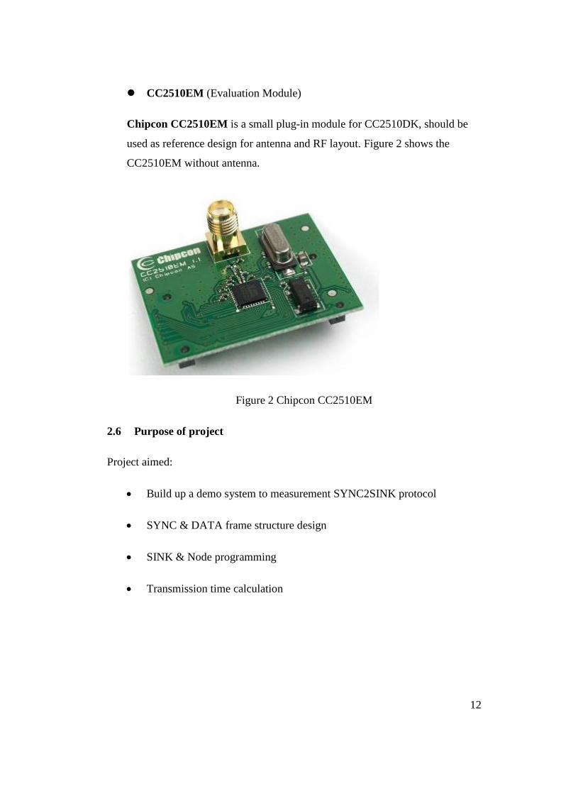
CC2510EM (Evaluation Module)
Chipcon CC2510EM is a small plug-in module for CC2510DK, should be
used as reference design for antenna and RF layout. Figure 2 shows the
CC2510EM without antenna.
Figure 2 Chipcon CC2510EM
2.6 Purpose of project
Project aimed:
Build up a demo system to measurement SYNC2SINK protocol
SYNC & DATA frame structure design
SINK & Node programming
Transmission time calculation

13
3 THEORTICAL BACKGROUND
3.1 SYNC&SINK protocol
The protocol stack is a global synchronization scheme and supports multi-hop
communications. The application requires multi-hop communication to send
sensed data back to a sink, and a global synchronization is necessary to offer time-
coherent noise information. [1]
SYNC2SINK works periodically and each period consists of two phases: SYNC
broadcasting, and data communication. Each period is started by the Sink node
broadcasting a SYNC frame, which contains a monotonically increasing sequence
number and the current time of the sink. Every node re-broadcasts the SYNC after
receiving a copy of it, and sets the sender of that SYNC as its predecessor to sink,
thus a passive route to sink is established for every node throughout the network.
3.2 Access testing environment
Wireless MCU development process in general as follows:
1. By using the software platform to preparation the testing program (source
code). The most commonly microcontroller developing software used IAR
development software platform. C language and C++ are both available to
use. In our case, we only need to use IAR EW and C language. After com-
plete the original programming by using IAR Embedded Workbench. I com-
piled source code into a *. HEX file which is able to operate inside the MCU.
2. Using an emulator to download *. HEX file to the appropriate MCU. In our
case, TI SmartRF Flash Programmer is the software we used to upload
*.HEX file.
3. The emulator will simulate the source program debugging. It will check the
source code, and help us to achieve the intended goal of developing tests. If
the program is correct, LCD will display the transmission time currently.

14
4. Running the program in wireless development system.
3.3 Architecture
Figure 3 is the block diagram for CC2510.
Figure 3 CC2510 Block diagram
As shown in Figure 3, the modules can be divided into one out of three categories:
CPU related modules, radio-related modules, and modules related to power, test,
15
and clock distribution. In the following subsections, a short description of each
module that appears in Figure 3. [10]
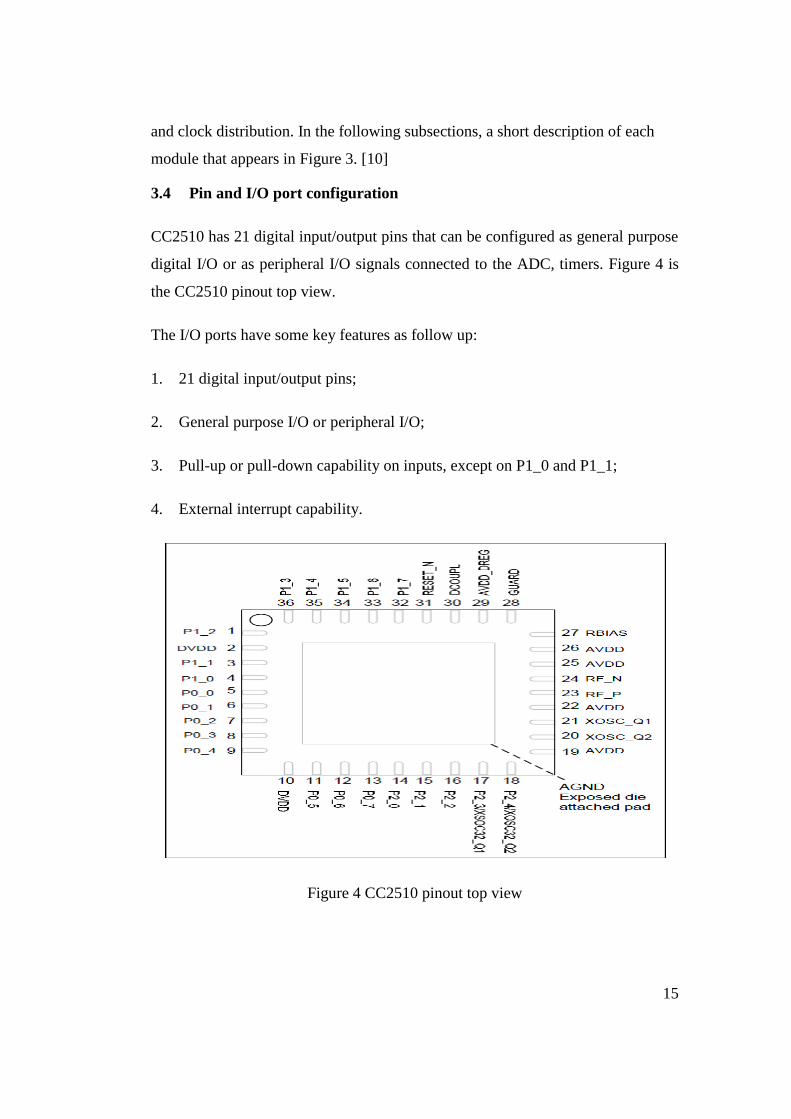
3.4 Pin and I/O port configuration
CC2510 has 21 digital input/output pins that can be configured as general purpose
digital I/O or as peripheral I/O signals connected to the ADC, timers. Figure 4 is
the CC2510 pinout top view.
The I/O ports have some key features as follow up:
1. 21 digital input/output pins;
2. General purpose I/O or peripheral I/O;
3. Pull-up or pull-down capability on inputs, except on P1_0 and P1_1;
4. External interrupt capability.
Figure 4 CC2510 pinout top view
16
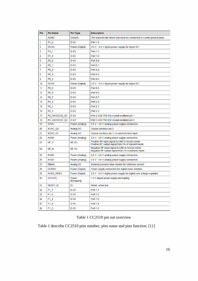
Table 1 CC2510 pin out overview
Table 1 describe CC2510 pins number, pins name and pins function. [11]
17
4 APPROACH AND IMPLEMENTATION
4.1 Hardware Setup
1. Plug CC2510EM into SmartRF04EB and Tan’s power supply board;
2. Connect antennas to both EM boards;
3. Plug USB cables to connect to computer for apply power supply and sniffer;
4. Press power on for check the standard setting.
5. First Board+ modular convert into a sniffer to capture packages when these
end devices are communication. [12][13].
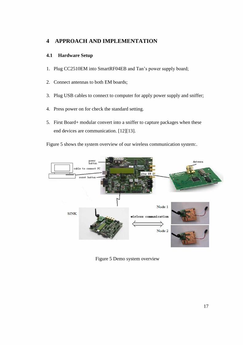
Figure 5 shows the system overview of our wireless communication system:.
Figure 5 Demo system overview
18
4.2 IAR Embedded Workbench Setup
IAREW is the most popular platform to develop embedded system application. Its
optimizing C/C++ compiler provides extensive support for a wide range of 8051
devices. The optimizing compilers generate very compact and efficient code. [14]
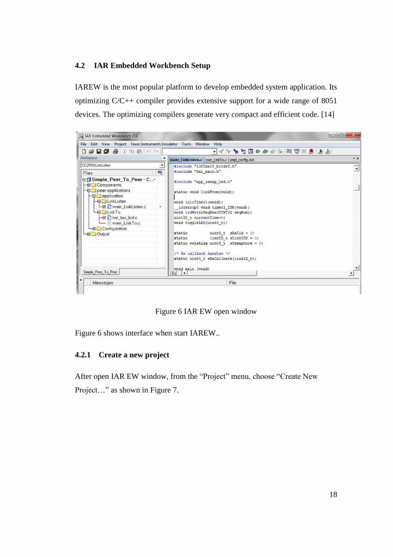
Figure 6 IAR EW open window
Figure 6 shows interface when start IAREW..
4.2.1 Create a new project
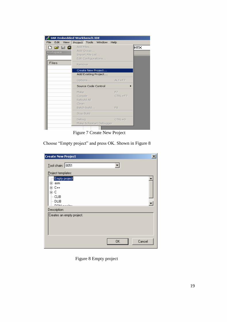
After open IAR EW window, from the “Project” menu, choose “Create New
Project…” as shown in Figure 7.
19
Figure 7 Create New Project
Choose “Empty project” and press OK. Shown in Figure 8
Figure 8 Empty project
20
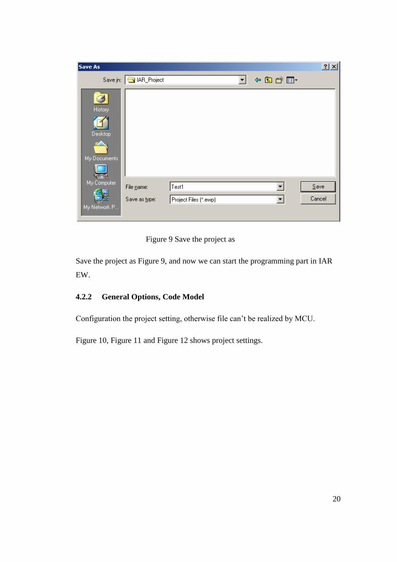
Figure 9 Save the project as
Save the project as Figure 9, and now we can start the programming part in IAR
EW.
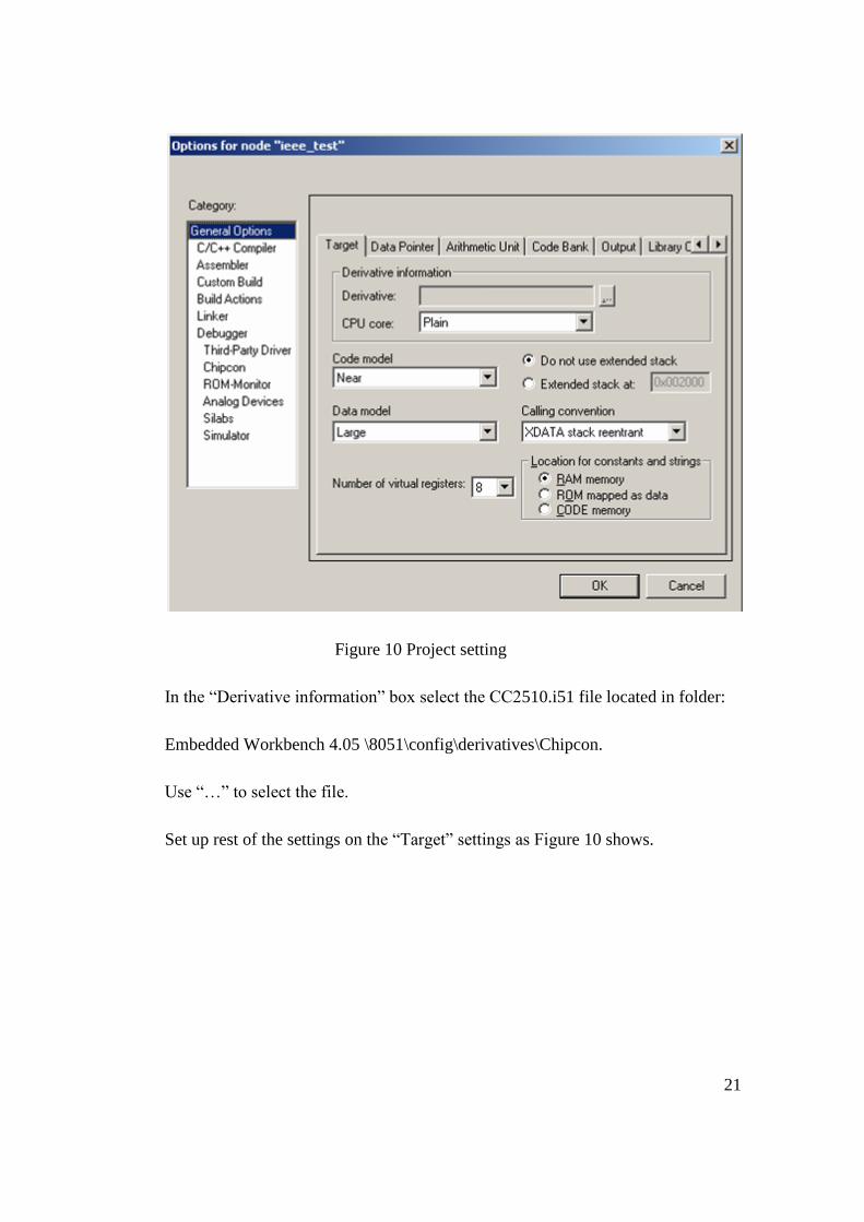
4.2.2 General Options, Code Model
Configuration the project setting, otherwise file can’t be realized by MCU.
Figure 10, Figure 11 and Figure 12 shows project settings.
21
Figure 10 Project setting
In the “Derivative information” box select the CC2510.i51 file located in folder:
Embedded Workbench 4.05 \8051\config\derivatives\Chipcon.
Use “…” to select the file.
Set up rest of the settings on the “Target” settings as Figure 10 shows.
22
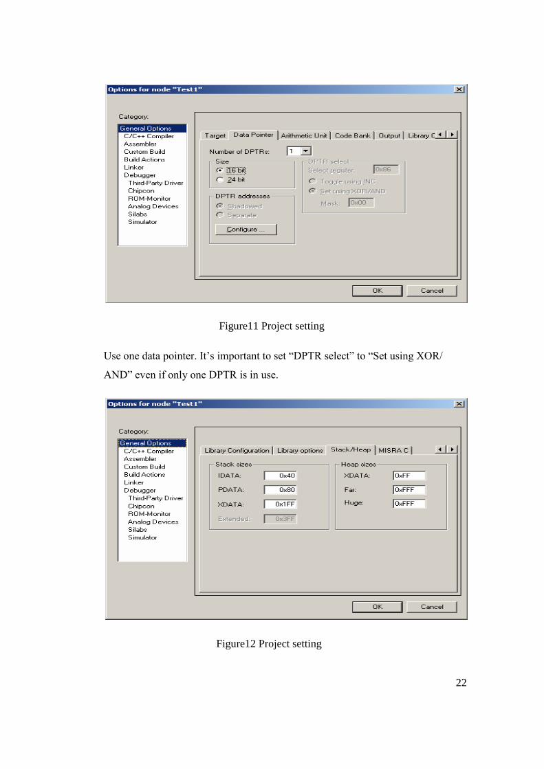
Figure11 Project setting
Use one data pointer. It’s important to set “DPTR select” to “Set using XOR/
AND” even if only one DPTR is in use.
Figure12 Project setting
23
Change XDATA stack size to 0x1FF.
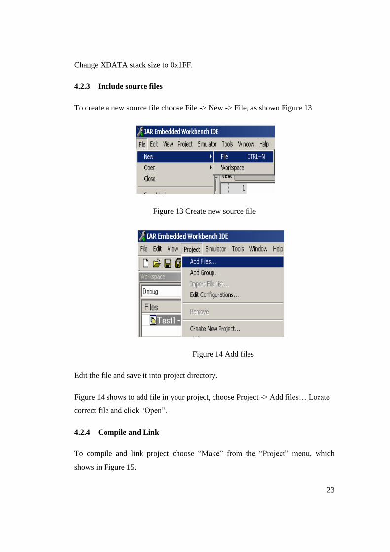
4.2.3 Include source files
To create a new source file choose File -> New -> File, as shown Figure 13
Figure 13 Create new source file
Figure 14 Add files
Edit the file and save it into project directory.
Figure 14 shows to add file in your project, choose Project -> Add files… Locate
correct file and click “Open”.
4.2.4 Compile and Link
To compile and link project choose “Make” from the “Project” menu, which
shows in Figure 15.

24
Figure 15 Compile and Link
4.3 TI SmartRF Programmer
Open TI SmartRF Programmer window shows above Figure 16:
Figure16 TI SmartRF Programmer

25
Figure17 transferring flow chart
As shown in figure 17, after finished the programming part, IAR EW will compile
the code and make it as *.HEX file, then open TI programmer, use this program-
mer to upload *.HEX file in MCU memory. MCU can only read *.HEX file.
4.4 TI SmartRF Studio
After we connect our sniffer node to the computer by using USB, open TI
SmartRF studio,

26
Figure18 TI SmartRF Studio
It will automatically detect device which you connected, make the highlight. In
Figure 18, CC2510 2.4GHz SoC is highlight, it also displays connected device
information at bottom list,.
27
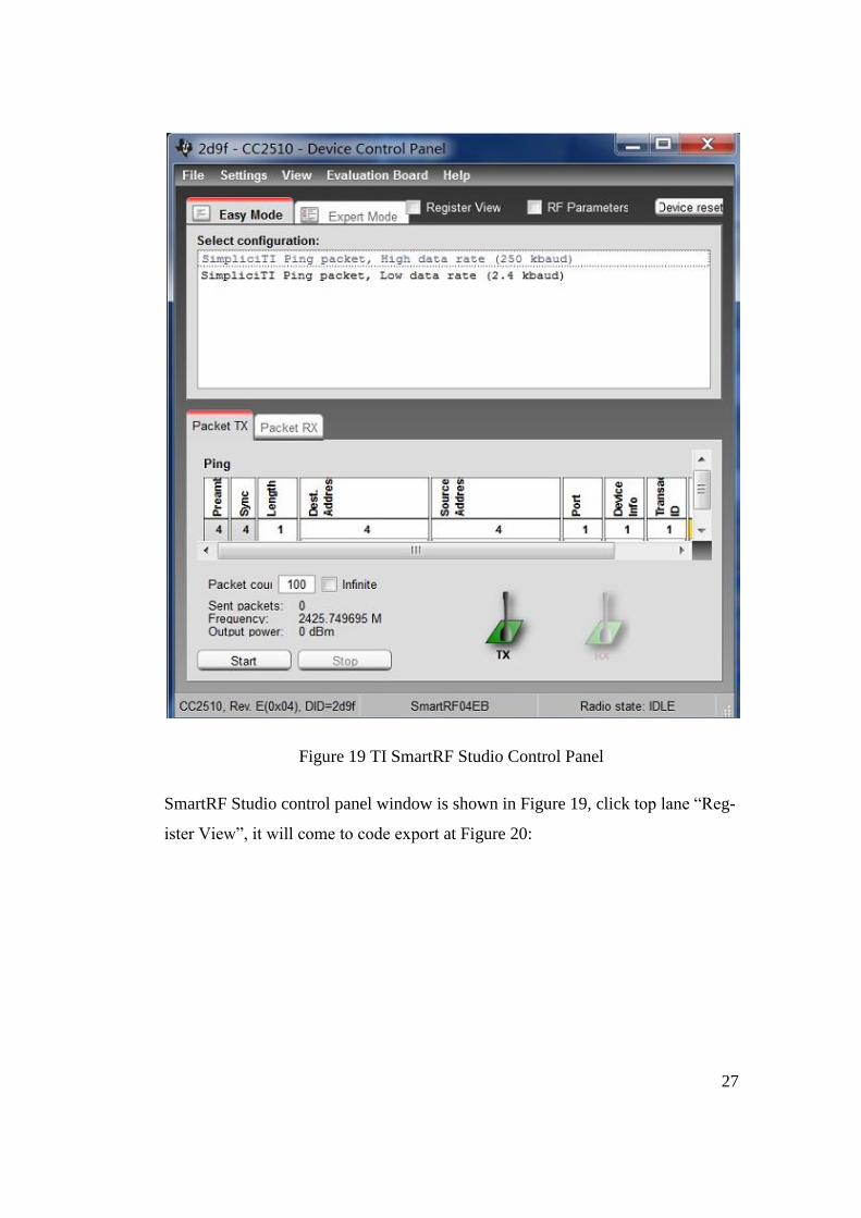
Figure 19 TI SmartRF Studio Control Panel
SmartRF Studio control panel window is shown in Figure 19, click top lane “Reg-
ister View”, it will come to code export at Figure 20:
28
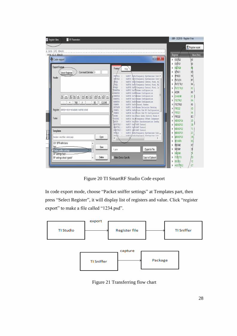
Figure 20 TI SmartRF Studio Code export
In code export mode, choose “Packet sniffer settings” at Templates part, then
press “Select Register”, it will display list of registers and value. Click “register
export” to make a file called “1234.psd”.
Figure 21 Transferring flow chart
29
Figure 21 is the transferring flow chart, which describe that when TI studio export
Register file, TI sniffer will realized the device register names, and then we can
start to capture packages.
Start demo WSN system, use TI SmartRF studio to export as register file, then TI
sniffer can recognize and capture packages.
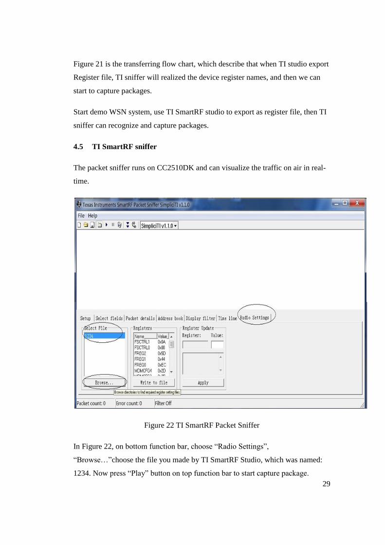
4.5 TI SmartRF sniffer
The packet sniffer runs on CC2510DK and can visualize the traffic on air in real-
time.
Figure 22 TI SmartRF Packet Sniffer
In Figure 22, on bottom function bar, choose “Radio Settings”,
“Browse…”choose the file you made by TI SmartRF Studio, which was named:
1234. Now press “Play” button on top function bar to start capture package.
30
4.6 Timer
In this section, I will describe the details how I created the timer for the program-
ming part. This timer controls the broadcasting time of the Sink.
4.6.1 Timer activity
• Control the time to send the frame
• Time interval between two consecutive arrives
• Fine time adjustment; ∆T= T’-T
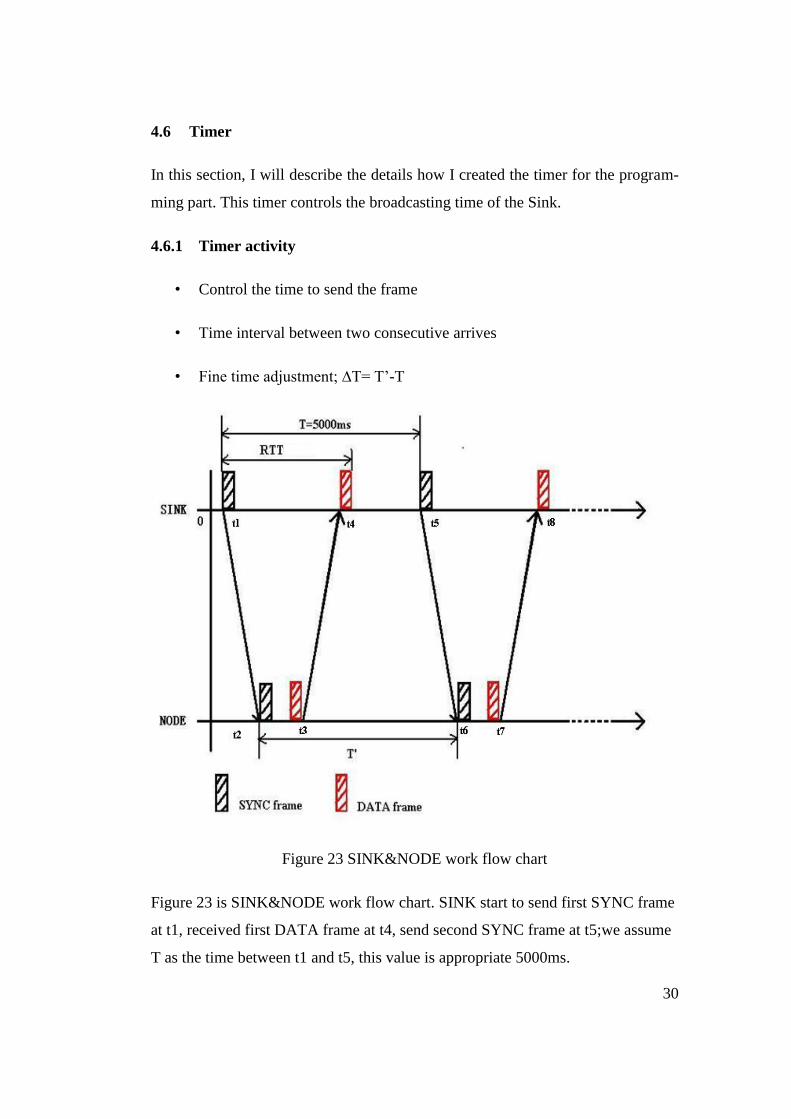
Figure 23 SINK&NODE work flow chart
Figure 23 is SINK&NODE work flow chart. SINK start to send first SYNC frame
at t1, received first DATA frame at t4, send second SYNC frame at t5;we assume
T as the time between t1 and t5, this value is appropriate 5000ms.

31
NODE received first SYNC frame at t2, start to send first DATA frame at t3, re-
ceived second SYNC frame at t6; we assume T´ as the time between t2 to t6, in
perfection state, T’ should be equal to T, but in practical situation, T´ >T, we cal-
culate delta: ∆t= T´-T.
RTT means Round Trip Time. It’s to define the transmission time between SINK
sends out the first SYNC frame and receives the first DATA frame.
4.6.2 Timer code
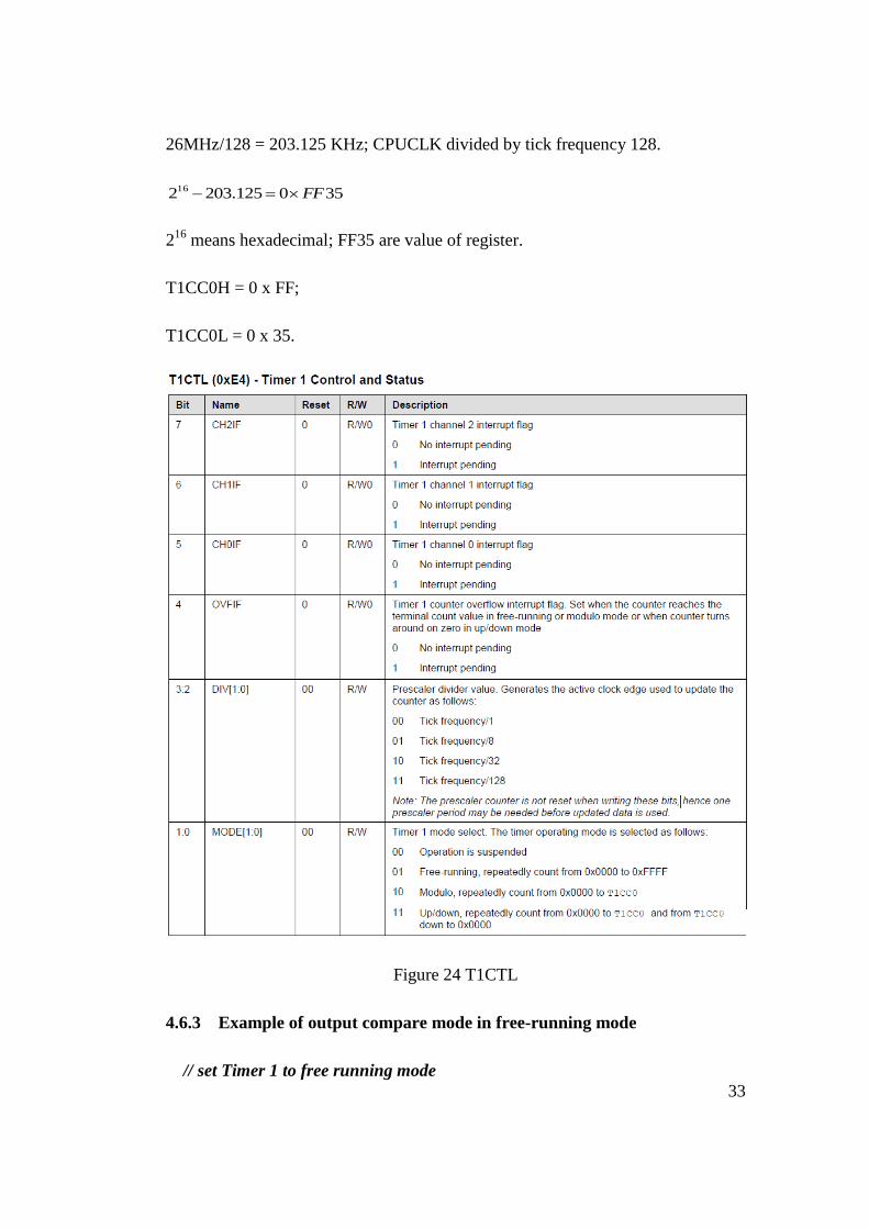
The control register T1CTL is used to control the timer operation. Six mode of
operation in follow: free-running mode, modulo mode, up/down mode, channel
mode control, input capture mode and output compare mode. Figure 24 shows the
T1CTL timer 1 control and status.
In output compare mode the I/O pin associated with a channel is set as an output.
After the timer has been started, the contents of the counter are compared with the
contents of the channel compare register T1CCnH:T1CCnL. If the compare regis-
ter equals the counter contents, the output pin is set, reset, or toggled according to
the compare output mode setting of T1CCTLn.CMP. Writing to the compare reg-
ister T1CCnL is buffered so that a value written to T1CCnL does not take effect
until the corresponding high order register, T1CCnH is written. For output com-
pare modes 0, a new value written to the compare registers T1CCnH:T1CCnL
takes effect after the registers have been written. [15]
Table 2 is CC2510Fx/CC2511Fx Specific SFR Overview.
Table 2 CC2510Fx/CC2511Fx Specific SFR Overview

32
// Set prescaler divider value to 8 to get a tickspeed of 101.56 kHz and
// set Timer 1 to free running mode
T1CTL = (T1CTL & ~(T1CTL_MODE|T1CTL_DIV)) |
T1CTL_MODE_FREERUN | T1CTL_DIV_8;
T1CTL &= ~T1CTL_CH0IF;
Code 1 timer code
To calculate value of T1CTL = 0x0D (in binary 00001101)
Count from left to right side,
0 -- No interrupt pending;
0 -- No interrupt pending;
0 -- No interrupt pending;
0 -- No interrupt pending;
11 -- Tick frequency/128;
01 -- Free-running, repeatedly count from 0x0000 to 0xFFFF.
// Set compare register of channel 0 to 32767 ( 0xFFFF / 2 )
T1CC0L = 0x35;
T1CC0H = 0xff;
Code 2 T1CC0L/T1CC0H value
This is the way I calculate T1CC0L/T1CC0H values:
CPUCLK = 26MHz;
33
26MHz/128 = 203.125 KHz; CPUCLK divided by tick frequency 128.
350125.203216 FF
216
means hexadecimal; FF35 are value of register.
T1CC0H = 0 x FF;
T1CC0L = 0 x 35.
Figure 24 T1CTL
4.6.3 Example of output compare mode in free-running mode
// set Timer 1 to free running mode
34
T1CTL = (T1CTL & ~(T1CTL_MODE | T1CTL_DIV))
|T1CTL_MODE_FREERUN
| T1CTL_DIV_8;
T1CTL &= ~T1CTL_CH0IF;
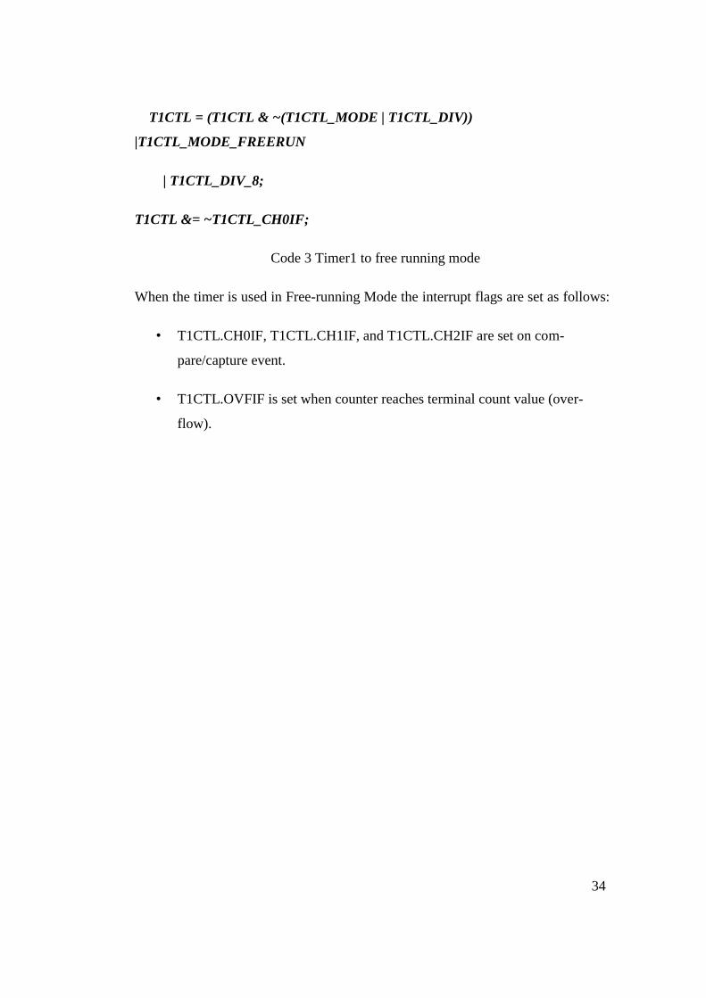
Code 3 Timer1 to free running mode
When the timer is used in Free-running Mode the interrupt flags are set as follows:
• T1CTL.CH0IF, T1CTL.CH1IF, and T1CTL.CH2IF are set on com-
pare/capture event.
• T1CTL.OVFIF is set when counter reaches terminal count value (over-
flow).

35
Figure 25 Output Compare Modes, Timer Free-running Mode
Timer 1 contains a 1-bit Delta-Sigma Modulator (DSM) of second order that can
be used to produce a mono audio output PWM (Pulse Width Modulator) signal.
The DSM removes the need for high order external filtering required when using
regular PWM mode.
The DSM operates at a fixed speed of either 1/4 or 1/8 of the timer tick speed set
by CLKCON.TICKSPD. The DSM speed is set by T1CCTL1.MODE. The input
samples are updated at a configurable sampling rate set by the terminal count val-
ue T1CC0. Figure 25 shows the output Compare modes, timer free-running mode.
36
4.7 SYNC structure
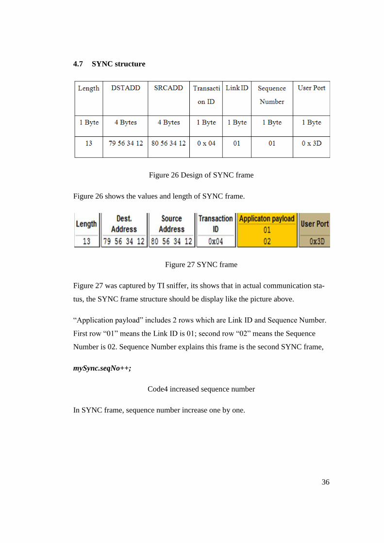
Figure 26 Design of SYNC frame
Figure 26 shows the values and length of SYNC frame.
Figure 27 SYNC frame
Figure 27 was captured by TI sniffer, its shows that in actual communication sta-
tus, the SYNC frame structure should be display like the picture above.
“Application payload” includes 2 rows which are Link ID and Sequence Number.
First row “01” means the Link ID is 01; second row “02” means the Sequence
Number is 02. Sequence Number explains this frame is the second SYNC frame,
mySync.seqNo++;
Code4 increased sequence number
In SYNC frame, sequence number increase one by one.
37
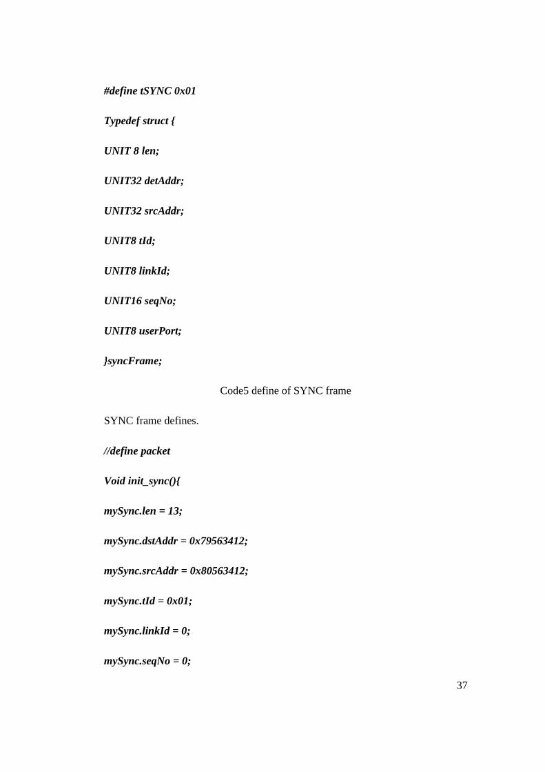
#define tSYNC 0x01
Typedef struct {
UNIT 8 len;
UNIT32 detAddr;
UNIT32 srcAddr;
UNIT8 tId;
UNIT8 linkId;
UNIT16 seqNo;
UNIT8 userPort;
}syncFrame;
Code5 define of SYNC frame
SYNC frame defines.
//define packet
Void init_sync(){
mySync.len = 13;
mySync.dstAddr = 0x79563412;
mySync.srcAddr = 0x80563412;
mySync.tId = 0x01;
mySync.linkId = 0;
mySync.seqNo = 0;

38
mySync.userPort = 0x3d;
}
Code6 SYNC fame initialized
Initialize SYNC frame in 8051 C language.
4.8 DATA structure
Figure 28 Design of DATA frame
Figure 28 shows the values and length of DATA frame.
Figure 29 DATA frame
Figure 29 was captured by TI sniffer, its shows that in actual communication sta-
tus, the DATA frame structure should be display like the picture above.
In DATA frame picture, Sequence Number is 02, which means this is the second
frame sent by NODE.

39
Typedef struct {
UNIT 8 len;
UNIT32 detAddr;
UNIT32 srcAddr;
UNIT8 tId;
UNIT8 linkId;
UNIT16 seqNo;
UNIT8 userPort;
}dataFrame;
Code7 Design of DATA frame
DATA frame is designed by using 8051 C language.
myData.seqNo++;
//define packet
Void init_data(){
my data.len = 13;
my data.dstAddr = 0x80563412;
my data.srcAddr = 0x79563412;
my data.tId = 0x01;
my data.linkId = 0;
my data.seqNo = 0;

40
my data.userPort = 0x20;
}
Code8 initial DATA fame
Initialize DATA frame in our program.

41
5 OUTCOME OF PROJECT
1. Design timer and frame;
The timer and SYNC frame/DATA frame structure can be used in my part-
ner’s project.
2. Demo system running success;
Base on Wireless Sensor Network type, my demo system composed by one
purpose computer, one sniffer device, and two end devices. At last 11 hours
testing, system works successful.
3. TI sniffer software captures frame matches.
Due to limited cell capacity, we run this system in11 hours; TI SmartRF snif-
fer captured over 15,000 packages.
packagepackage
packageond
hourondhours
1584027920
7920sec5
/sec360011
In perfect state, TI sniffer should capture 15840 packages (SINK+NODE).
But after counting the packages we captured, we found that we only received
7913 SNYC frames and 7917 DATA frames. That means 10 packages are lost
during the transmission.

42
6 CONCLUSIONS AND DISCUSSION
By doing this project, I learned a lot:
1. Start to learn 8051 C language;
2. To master and use newly software via searching and reading instruction.
3. Get initial values of the registers by checking TI’s datasheet.
4. Patience testing during project met troubles.
After testing our system, the packets which captured with TI sniffer are totally
matched our design, this result proves our communication system works in a cor-
rect way and the design of SYNC/DATA structure is working properly.
Weakness:
I know less of 8051 C language at the beginning of this project; and it’s my first
time to use TI SmartRF programmer, studio, sniffer, and IAR EW platform. In
order calculate register values I have to check a lot of TI datasheet.
Further development:
1. Modify per-to-per mode, and update the transmission mode to TDMA.
2. Increase the function of sensors; the nodes are able to detect data of tempera-
ture, electromagnetic, earthquakes, humidity, noise levels, lighting intensity,
pressure, soil composition, movement object size and so on.
3. Because of limited coverage and communication range, WSN must have large
numbers of sensor; it’s very difficult to recharge/replace battery. In order to
extend sensor/network work life, all the nodes can be put into SLEEP mode
when they are not working.

43
REFERENCES
/1/ Ismo Hakala, Ilkka Kivel, Jukka Ihalainen, Jari Luomala, Chao Gao. De-
sign of Low-Cost Noise Measurement Sensor Network: Sensor Function Design.
University Of Jyväskylä, Kokkola University Consortium Chydenius, FI-67701,
Kokkola, Finland [referred 22.11.2010] Available on the Internet:
<URL:http://www.cc.puv.fi/~gc/download/publications/Design_of_Low-
Cost_Noise_Measurement_Sensor_Network_Sensor_Function_Design.pdf >
/2/ Arnold, B. Embedded System Design. (2002) [referred 12.01.2011] Avail-
able on the Internet:
<URL:http://books.google.com/books?id=3vY35UkvXrAC&printsec=frontcover
&source=gbs_ge_summary_r&cad=0#v=onepage&q&f=false >.
/3/ Ilker Demirkol, Cem Ersoy, and Fatih Alagöz (20 Dec 2001) MAC Proto-
cols for Wireless Sensor Networks: a Survey. [referred 05.05.2011]. Available on
Internet: <URL: http://ieeexplore.ieee.org/xpls/abs_all.jsp?arnumber=1632658>.
/4/ I.F. Akyildiz, W. Su, Y. Sankarasubramaniam, E. Cayirci. Wireless sensor
networks: a survey (2002). Broadband and Wireless Networking Laboratory,
School of Electrical and Computer Engineering, Georgia Institute of Technology,
USA. [referred 03.05.2011]. Available on the Internet: <URL:
http://linkinghub.elsevier.com/retrieve/pii/S1389128601003024>.
/5/ Texas Instruments (11 Jul 2008) Low-Power SoC (System-on-Chip) with
MCU, memory, 2.4GHz RF Transceiver, and USB (Rev.F). [referred 03.05.2010].
Available on Internet: <URL:
http://focus.ti.com/docs/prod/folders/print/cc2510f16.html>.
/6/ IAR Embedded Workbench for 8051 (30 Jun 2010) IAR Embedded
Workbench for 8051 Version 7.60. [referred 03.05.2010]. Available on Internet:
<URL: http://www.iar.com/website1/1.0.1.0/244/1/>.
44
/7/ Texas Instruments (13 Apr 2011) SmartRF Flash Programmer 1.11.1
(Rev.M). [referred 20.04.2011]. Available on Internet: <URL:
http://focus.ti.com/docs/toolsw/folders/print/flash-programmer.html>.
/8/ Texas Instruments (21 Feb 2011) SmartRF Studio 7 v1.4.9 (Rev.H). [re-
ferred 12.03.2011]. Available on Internet:
<URL:http://focus.ti.com/docs/toolsw/folders/print/smartrftm-studio.html>.
/9/ Texas Instruments (01 Dec 2008) SimpliciTI Overview (Rev.B). [referred
12.03.2011]. Available on Internet: <URL:http://www.ti.com/litv/pdf/swru130b>.
/10/ Texas Instruments (10 Apr 2008) Low-Power SoC (System-on-Chip) with
MCU, Memory, 2.4 GHz RF Transceiver, and USB Controller v1.3(Rev.E). [re-
ferred 03.04.2010]. Available on Internet: <URL:
http://focus.ti.com/lit/ds/swrs055f/swrs055f.pdf >.
/11/ Texas Instruments (11 Jul 2008) Low-Power SoC (System-on-Chip) with
MCU, memory, 2.4GHz RF Transceiver, and USB (Rev.F). [referred 03.04.2010].
Available on Internet: <URL: http://focus.ti.com/lit/ds/symlink/cc2510f32.pdf>.
/12/ Texas Instruments (14 Dec 2007) CC2510-CC2511DK --Development Kit
User Manual (Rev. A). [referred 27.03.2010]. Available on Internet: <URL:
http://www.ti.com/litv/pdf/swru134a>.
/13/ Texas Instruments (02 Sep 2010) CC2510-CC2511 DK Quick Start (Rev.
B). [referred 15.04.2010]. Available on Internet: <URL:
http://www.ti.com/litv/pdf/swru079b>.
/14/ IAR Embedded Workbench for 8051 (30 Jan 2006) IAR IDE User Manual.
[referred 15.04.2010]. Available on Internet: <URL:
http://www.ti.com/litv/pdf/swru038>.
/15/ Texas Instruments (24 Aug 2010) CC2510EM Reference Design 3.0 (Rev.
B). [referred 03.09.2010]. Available on Internet: <URL:
http://www.ti.com/litv/zip/swrr035b>.