Embed Size (px)
Citation preview
1
Sensores Integrados em Silício IE325 EE824
Professor Fabiano Fruett
UNICAMP – FEEC - DSIFSala 207
www.dsif.fee.unicamp.br/~fabiano
Propriedades mecânicas do silício
Referências
F. Fruet and G. C. M. Meijer, "The piezojunction effect in silicon integrated circuits and sensors", Kluwer, 2002
http://www.ioffe.rssi.ru/SVA/NSM/Semicond/Si/
2
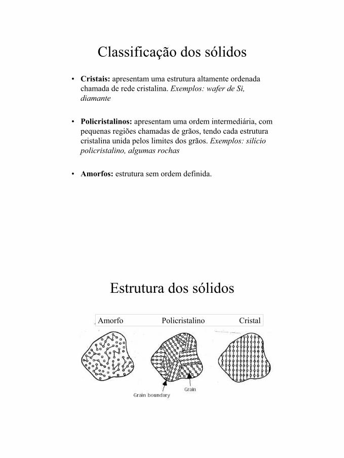
Classificação dos sólidos
• Cristais: apresentam uma estrutura altamente ordenada chamada de rede cristalina. Exemplos: wafer de Si, diamante
• Policristalinos: apresentam uma ordem intermediária, com pequenas regiões chamadas de grãos, tendo cada estrutura cristalina unida pelos limites dos grãos. Exemplos: silício policristalino, algumas rochas
• Amorfos: estrutura sem ordem definida.
Estrutura dos sólidos
Amorfo Policristalino Cristal
3
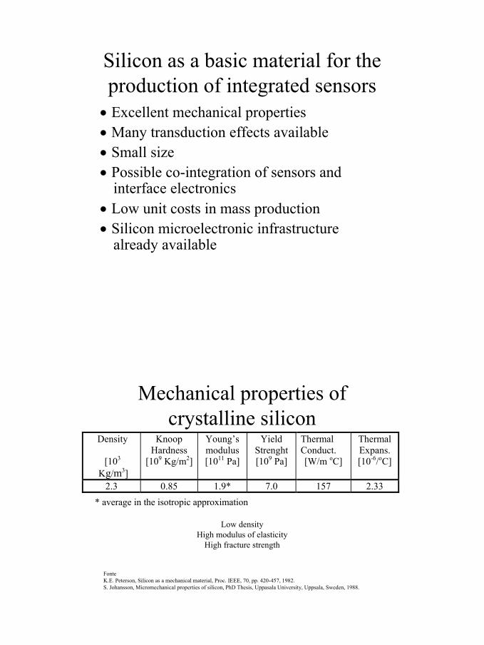
Silicon as a basic material for the production of integrated sensors• Excellent mechanical properties• Many transduction effects available• Small size• Possible co-integration of sensors and
interface electronics• Low unit costs in mass production• Silicon microelectronic infrastructure
already available
Mechanical properties of crystalline silicon
Density
[103 Kg/m3]
Knoop Hardness
[109 Kg/m2]
Young’s modulus [1011 Pa]
Yield Strenght [109 Pa]
Thermal Conduct. [W/m oC]
Thermal Expans. [10-6/oC]
2.3 0.85 1.9* 7.0 157 2.33 * average in the isotropic approximation
Fonte K.E. Peterson, Silicon as a mechanical material, Proc. IEEE, 70, pp. 420-457, 1982.S. Johansson, Micromechanical properties of silicon, PhD Thesis, Uppasala University, Uppsala, Sweden, 1988.
Low density High modulus of elasticity
High fracture strength
4
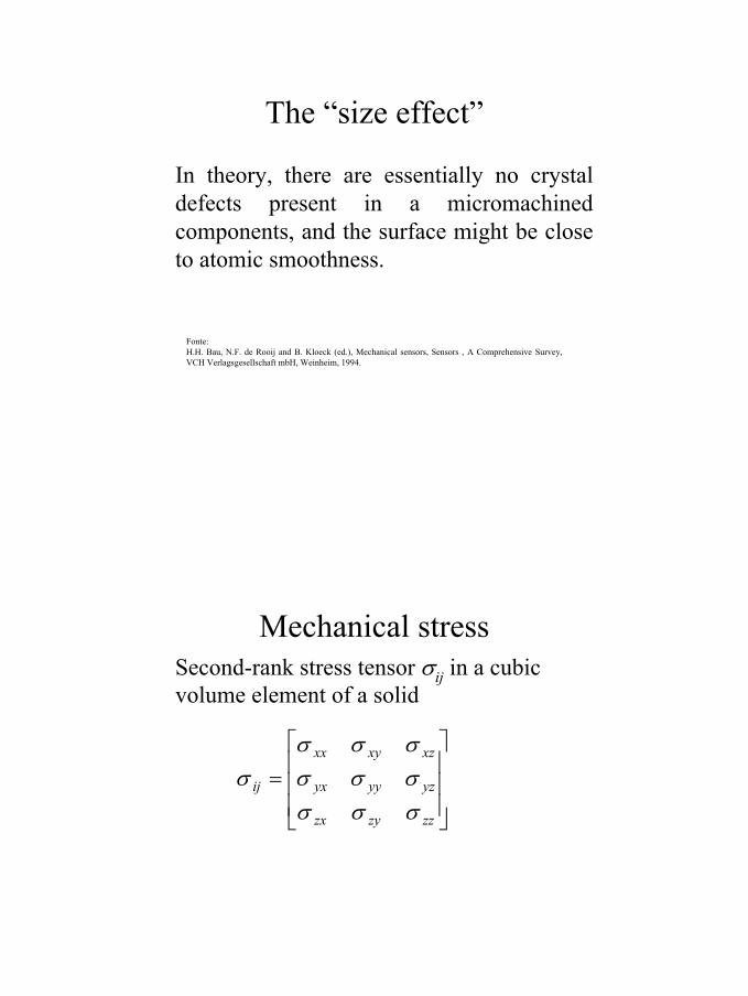
The “size effect”
In theory, there are essentially no crystal defects present in a micromachinedcomponents, and the surface might be close to atomic smoothness.
Fonte: H.H. Bau, N.F. de Rooij and B. Kloeck (ed.), Mechanical sensors, Sensors , A Comprehensive Survey, VCH Verlagsgesellschaft mbH, Weinheim, 1994.
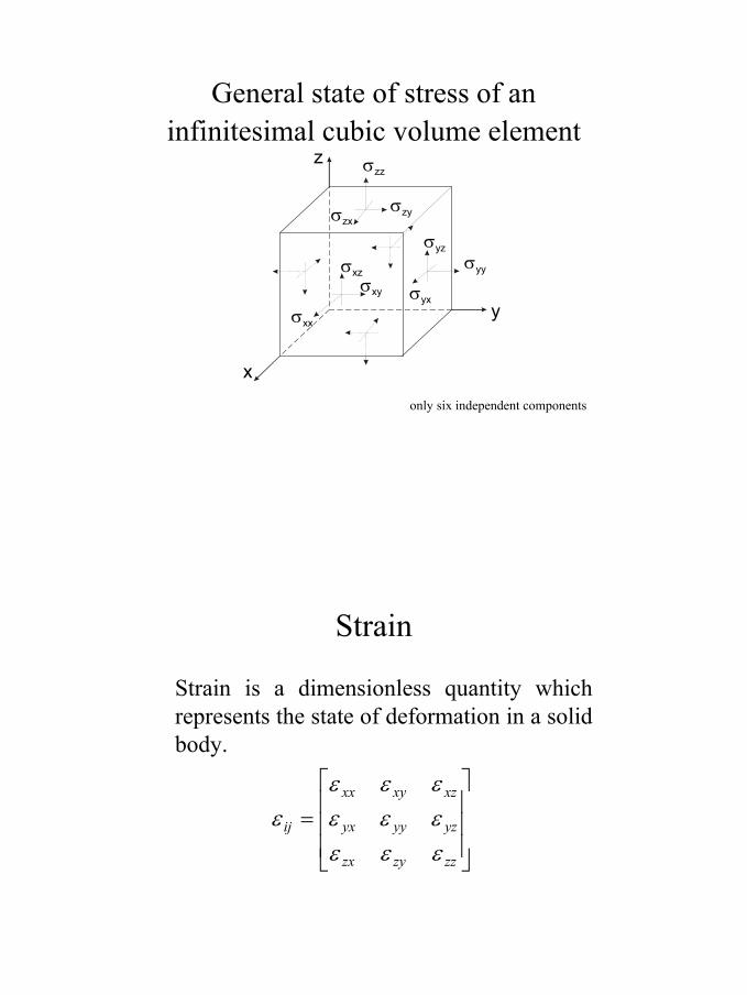
Mechanical stressSecond-rank stress tensor σij in a cubic volume element of a solid
=
zzzyzx
yzyyyx
xzxyxx
ij
σσσσσσσσσ
σ
5
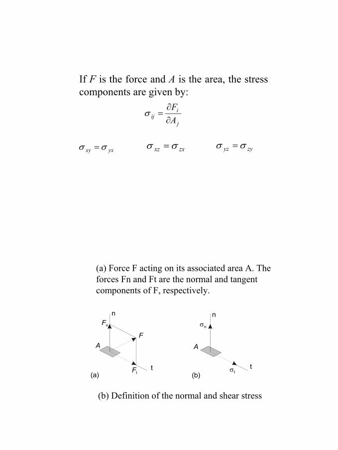
If F is the force and A is the area, the stress components are given by:
j
iij A
F∂∂
=σ
yxxy σσ = zxxz σσ = zyyz σσ =
(a) Force F acting on its associated area A. The forces Fn and Ft are the normal and tangent components of F, respectively.
(b) Definition of the normal and shear stress
Fn
n n
F
t tFt
A A
σn
σt(a) (b)
6
General state of stress of an infinitesimal cubic volume element
y
x
z σzz
σzyσzx
σyy
σyz
σyx
σxx
σxy
σxz
only six independent components
Strain
Strain is a dimensionless quantity which represents the state of deformation in a solid body.
=
zzzyzx
yzyyyx
xzxyxx
ij
εεεεεεεεε
ε
7
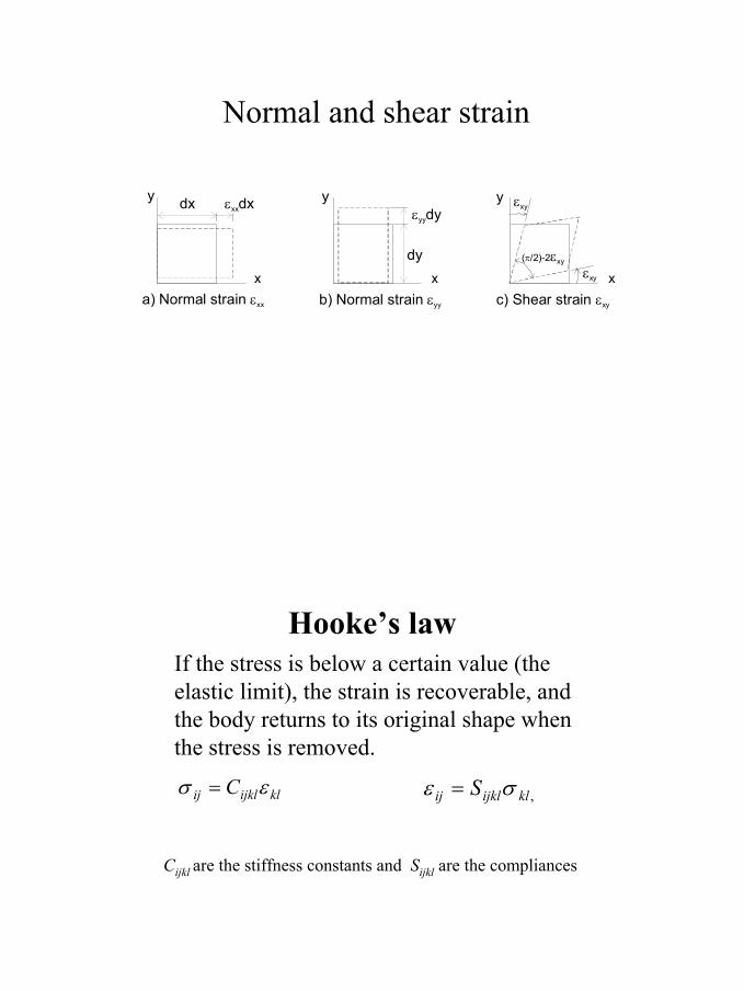
Normal and shear strain
a) Normal strain εxx b) Normal strain εyy c) Shear strain εxy
dx
dy
εxxdxεyydy
x x x
y y y
εxy
εxy
( /2)-2π εxy
Hooke’s lawIf the stress is below a certain value (the elastic limit), the strain is recoverable, and the body returns to its original shape when the stress is removed.
klijklij C εσ = ,klijklij S σε =
Cijkl are the stiffness constants and Sijkl are the compliances
8
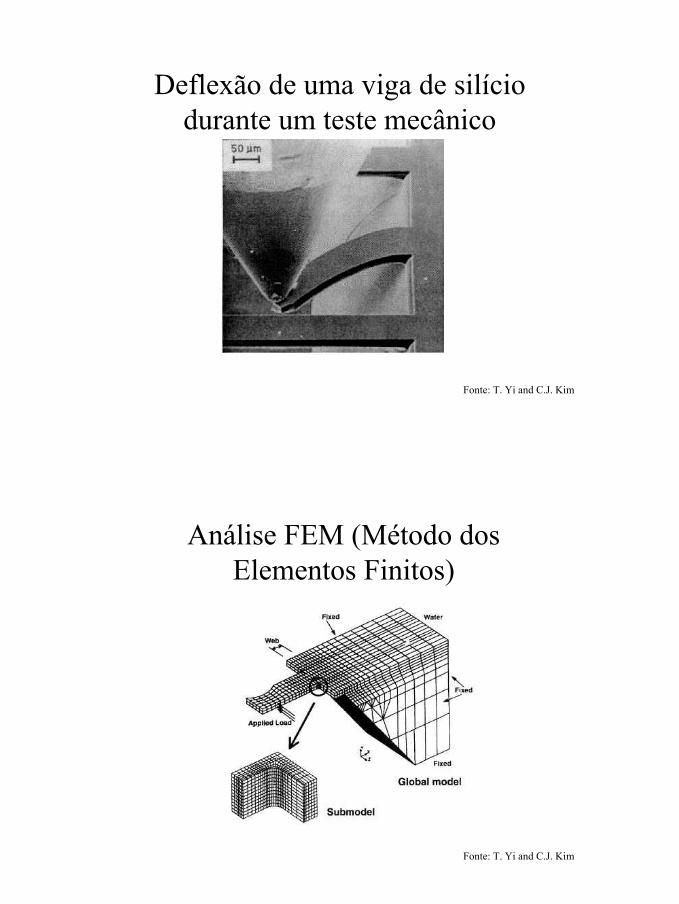
Deflexão de uma viga de silício durante um teste mecânico
Fonte: T. Yi and C.J. Kim
Análise FEM (Método dos Elementos Finitos)
Fonte: T. Yi and C.J. Kim
9
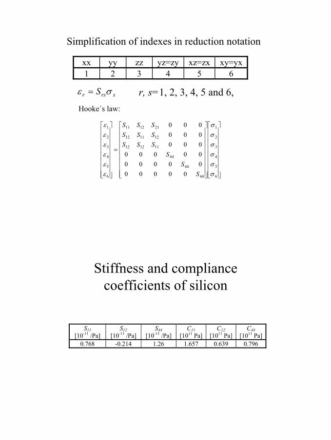
Simplification of indexes in reduction notation
r, s=1, 2, 3, 4, 5 and 6,
xx yy zz yz=zy xz=zx xy=yx1 2 3 4 5 6
srsr S σε =
=
6
5
4
3
2
1
44
44
44
111212
121112
211211
6
5
4
3
2
1
000000000000000000000000
σσσσσσ
εεεεεε
SS
SSSSSSSSSS
Hooke´s law:
Stiffness and compliance coefficients of silicon
S11 [10-11 /Pa]
S12 [10-11 /Pa]
S44 [10-11 /Pa]
C11 [1011 Pa]
C12 [1011 Pa]
C44 [1011 Pa]
0.768 -0.214 1.26 1.657 0.639 0.796
10
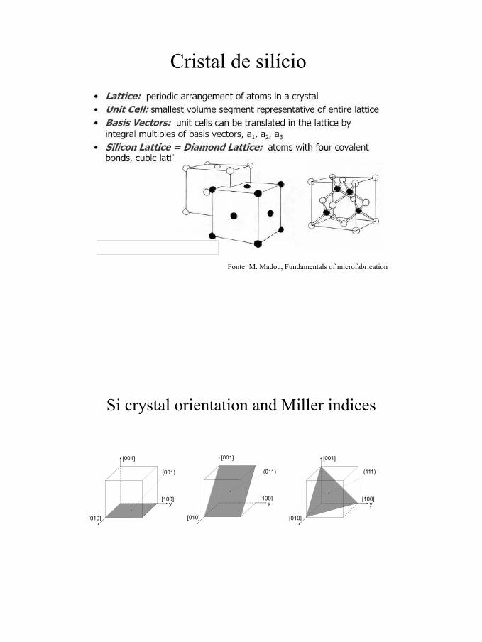
Cristal de silício
Silicon has the same crystal structure as diamond.
Fonte: M. Madou, Fundamentals of microfabrication
Si crystal orientation and Miller indices
y
[001]
[100]
(001)
[010]
y
[001]
[100]
(011)
[010]
y
[001]
[100]
(111)
[010]
11
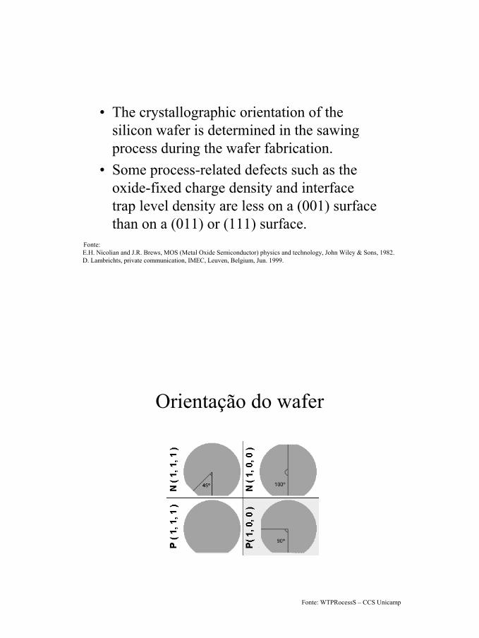
• The crystallographic orientation of the silicon wafer is determined in the sawing process during the wafer fabrication.
• Some process-related defects such as the oxide-fixed charge density and interface trap level density are less on a (001) surface than on a (011) or (111) surface.
Fonte:E.H. Nicolian and J.R. Brews, MOS (Metal Oxide Semiconductor) physics and technology, John Wiley & Sons, 1982.D. Lambrichts, private communication, IMEC, Leuven, Belgium, Jun. 1999.
Orientação do wafer
Fonte: WTPRocessS – CCS Unicamp
12
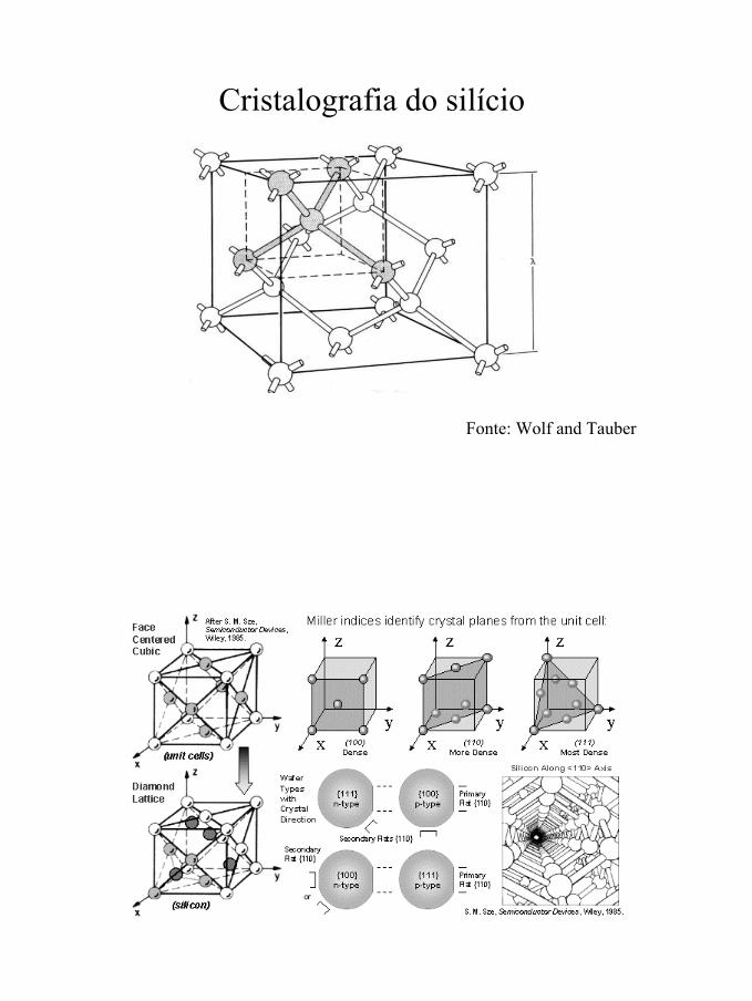
Cristalografia do silício
Fonte: Wolf and Tauber
13
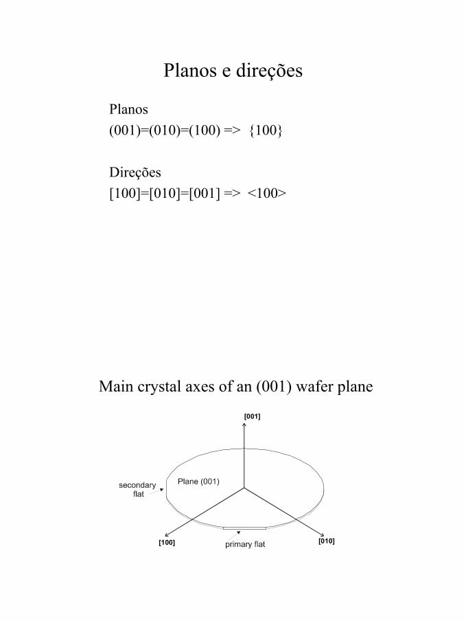
Planos e direções
Planos(001)=(010)=(100) => {100}
Direções[100]=[010]=[001] => <100>
Main crystal axes of an (001) wafer plane
[100] [010]
[001]
14
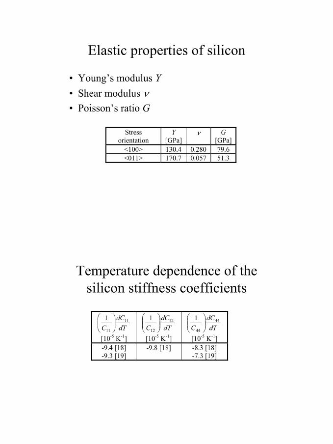
Elastic properties of silicon
• Young’s modulus Y• Shear modulus ν• Poisson’s ratio G
Stress orientation
Y [GPa]
ν G [GPa]
<100> 130.4 0.280 79.6 <011> 170.7 0.057 51.3
Temperature dependence of the silicon stiffness coefficients
dTdC
C11
11
1
[10-5 K-1] dT
dCC
12
12
1
[10-5 K-1] dT
dCC
44
44
1
[10-5 K-1] -9.4 [18] -9.3 [19]
-9.8 [18]
-8.3 [18] -7.3 [19]
15
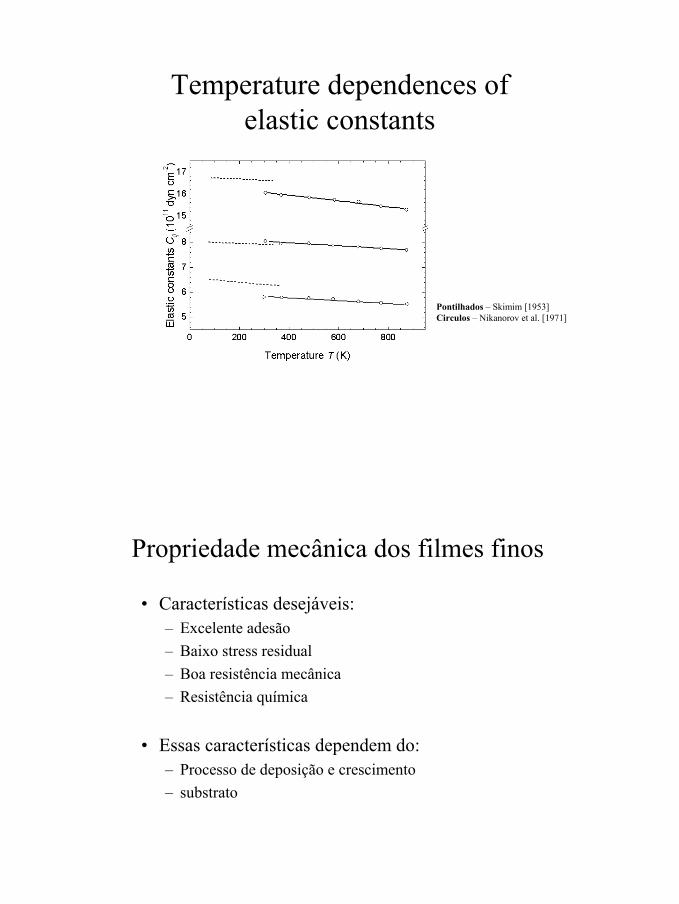
Temperature dependences of elastic constants
Pontilhados – Skimim [1953]Circulos – Nikanorov et al. [1971]
Propriedade mecânica dos filmes finos
• Características desejáveis:– Excelente adesão– Baixo stress residual– Boa resistência mecânica– Resistência química
• Essas características dependem do:– Processo de deposição e crescimento– substrato
16
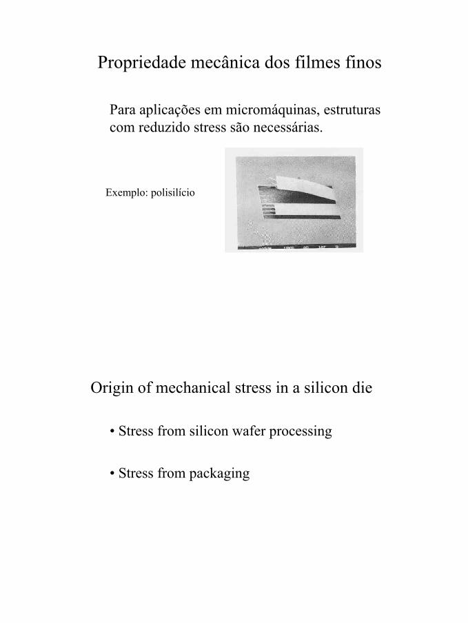
Propriedade mecânica dos filmes finos
Para aplicações em micromáquinas, estruturas com reduzido stress são necessárias.
Exemplo: polisilício
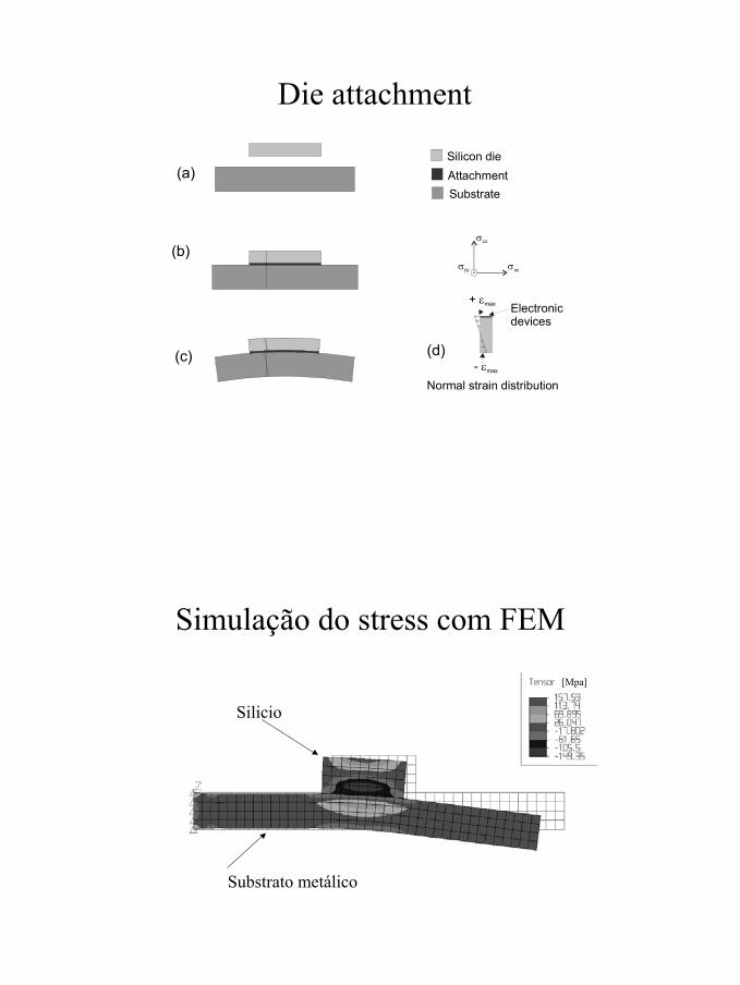
Origin of mechanical stress in a silicon die
• Stress from silicon wafer processing
• Stress from packaging
17
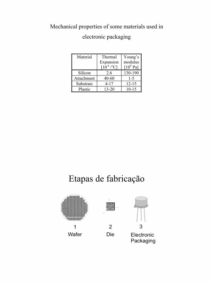
Mechanical properties of some materials used in
electronic packaging
Material Thermal Expansion [10-6 /oC]
Young’smodulus[109 Pa]
Silicon 2.6 130-190Attachment 40-60 1-5 Substrate 4-17 12-15
Plastic 13-20 10-15
Etapas de fabricação
Wafer Die ElectronicPackaging
1 2 3
18
Die attachment
Silicon dieAttachmentSubstrate
+ εmax
- εmax
Normal strain distribution
Electronic devices
(b)
(c) (d)
(a)
σxxσyy
σzz
Simulação do stress com FEM
[Mpa]
Substrato metálico
Silicio
19
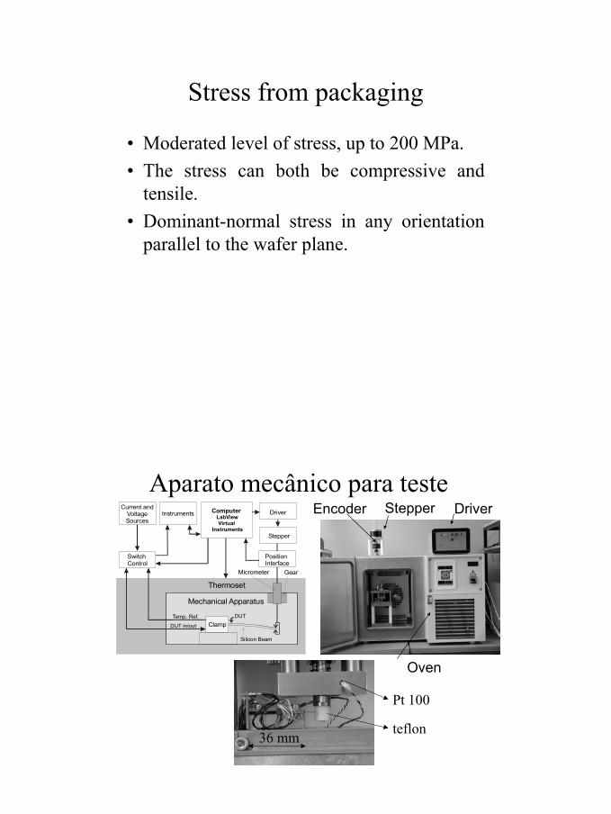
Stress from packaging
• Moderated level of stress, up to 200 MPa.• The stress can both be compressive and
tensile.• Dominant-normal stress in any orientation
parallel to the wafer plane.
Aparato mecânico para teste
Silicon Beam
Switch Control
Current andVoltageSources
Instruments Computer LabView
Virtual Instruments
Driver
Stepper
Mechanical Apparatus
Position Interface
Micrometer Gear
ClampDUT in/out
DUT Temp. Ref.
Thermoset
DriverStepperEncoder
Oven
36 mm teflon
Pt 100
20
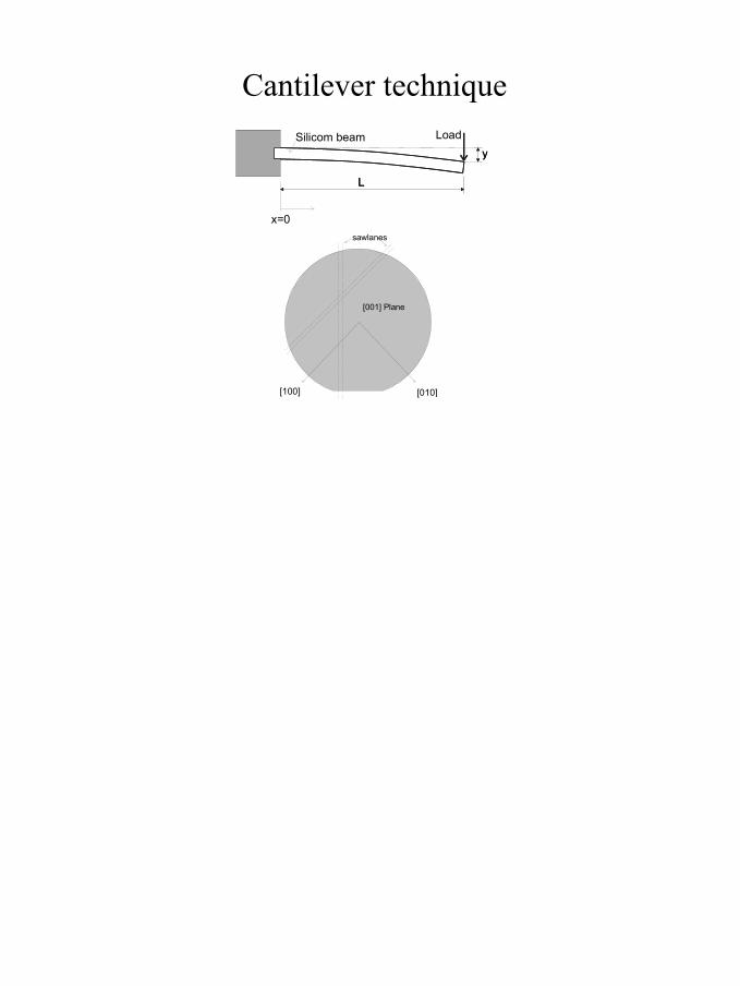
Cantilever technique
L
x=0
y
L
yLoadSilicom beam
[100] [010]
[001] Plane
sawlanes