Embed Size (px)
Citation preview
IEEE TRANSACTIONS ON MICROWAVE THEORY AND TECHNIQUES. VOL. 31. NO. 4, APRIL 1989 71 1
Propagation in Layered Biased Semiconductor Structures Based on Transport Analysis
Abstract -A transport-field parallel-plate formulation and solution method to determine the small-signal propagation constant is given for wide microstrip lines over an inhomogeneously doped semiconductor sub- strate of small transverse dimensions. Included in the detailed transport model are two carrier species, recombination-generation mechanisms, dc and ac field-dependent mobilities and diffusion constants, and boundary condition contact effects. A transverse dc bias condition is applied. Struc- tures numerically simulated are a voltage-variable GaAs distributed Schottky barrier phase shifter and a transmission line over a Si bipolar junction. Numerical data based on a finite difference technique are gener- ated on carrier densities, electric potentials and fields, and current densi- ties. Propagation constant calculations were favorably compared with those calculated by both full-wave field analysis and moments-of-the-Boltz- mann-equation analysis for some less general cases. y results for the GaAs structure are compared with available experimental data.
I. INTRODUCTION AVEGUIDING structures loaded with extrinsic W semiconductor material are utilized in both mono-
lithic microwave integrated circuits (MMIC's) and hgh- speed digital large scale integrated (LSI) and very large scale integrated (VLSI) circuits. Distributed FET and IM- PATT amplifiers, voltage-variable phase shifters, and tun- able attenuators are several examples of distributed MMIC devices which employ the interaction of the charge carriers with the electromagnetic fields in semiconductors [ 11-[4]. Also, microstrip and coplanar transmission lines over lay- ered semiconductor media are used for interconnections between active devices in MMIC and VLSI technologies. The interconnections generally lie over passive semicon- ductor material, except in the vicinity of active devices where a transition region exists.
Analysis of metal-insulator-semiconductor (MIS) trans- mission lines and distributed Schottky contact lines has been carried out in the past with field approaches utilizing a single constant conductivity to model each doped semi- conductor layer [5]-[9]. These field approaches, which range in complexity from quasi-TEM to full-wave analy- ses, have been successful in predicting the performance of MIS structures and uniformly doped, biased Schottky structures. T h s success is due to the lack of transverse currents because of a distinct insulator-semiconductor in- terface (MIS structures) and uniform conductivities in
Manuscript received February 16, 1988; revised October 26, 1988. The authors are with the Electronics Science and Technology Division,
IEEE Log Number 8826041. Naval Research Laboratory, Washington, DC 20375-5000.
individual semiconductor bulk layers (MIS and Schottky structures). When the semiconductor volume contains sev- eral junctions (such as pn and n+ n) or intentionally graded doped areas, the constant-conductivity assumption no longer always represents the transverse transport accu- rately.
For example, diffusion of carriers away from the transi- tional zones between bulk and space-charge depletion re- gions in the vicinity of a junction causes a change in the field-carrier interaction within a few Debye lengths of each regional interface. Static dc characteristics as well as ac characteristics of the transport behavior will be altered. As a result, wave propagation behavior will also be changed. These additional considerations are especially important for structures whch have very small transverse dimen- sions, such as micron and submicron feature sizes, which are increasingly seen in higher frequency (millimeter wave), hgher speed (GHz digital and logic pulse), or denser circuits.
In this paper a transport-field parallel-plate formulation and solution method to find the small-signal propagation constant y is presented for wide microstrip lines (with respect to transverse dimensions) over an inhomoge- neously doped semiconductor substrate. The formulation approach includes dual carrier transport (electrons and holes); recombination-generation mechanisms (direct band gap, Shockley-Read-Hall, and Auger); dc and ac field- dependent carrier mobilities ( p n ( E ) , pP( E ) , pnu( E ) , and pPu( E)); field-dependent diffusion constants (On( E ) and D,(E)); and boundary condition contact effects at the guiding structure walls (ohmic and Schottky contacts). The E-field dependence of mobility is important since it allows negative differential conductivity to occur in some regions of a structure possessing a 111-V semiconductor material.
The theoretical approach contained herein avoids the aforementioned difficulties when a field-transport model possessing an oversimplified transport description of the carriers is used. Section I1 covers the construction of the field-transport model of the microstrip structure. A simul- taneous set of coupled ac equations are obtained which describe TM, electromagnetic propagation. The method yields the dominant mode propagation constant y for the strip over passive or active semiconductor substrates and retains dispersion through a detailed transport model. Sec- tion I11 discusses the numerical finite difference technique
U.S. Government work not protected by U.S. copyright
712 IEEE TRANSACTIONS ON MICROWAVE THEORY AND TECHNIQUES, VOL. 37, NO. 4, APRIL 1989
electron and hole current density vectors, the electron and hole net recombination rates, and the electronic charge magnitude. R , = R , = R is specified to avoid a net sink (or source) of charge (subtract (2b) from (2a) to see this point). A local field representation is used for J, and J,: CONDUCTOR z
x = o W Y J, = - gnu, + qD,Vn ( 3 4 INHOMOGENEOUS SEMICONDUCTOR
x = P ' GROUND-PLANE
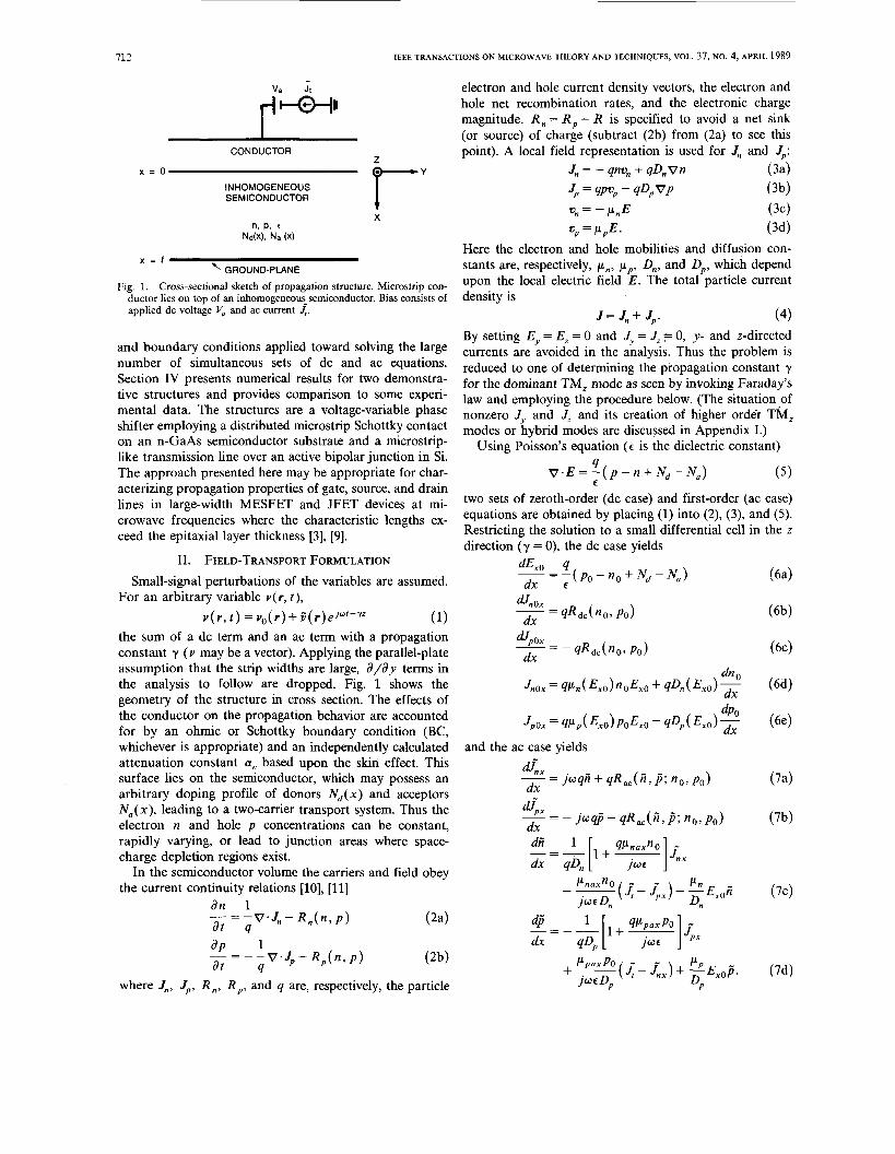
Fig. 1. Cross-sectional sketch of propagation structure. Microstrip con- ductor lies on top of an inhomogeneous_semiconductor. Bias consists of applied dc voltage Vu and ac current J,.
and boundary conditions applied toward solving the large number of simultaneous sets of dc and ac equations. Section IV presents numerical results for two demonstra- tive structures and provides comparison to some experi- mental data. The structures are a voltage-variable phase shfter employing a distributed microstrip Schottky contact on an n-GaAs semiconductor substrate and a microstrip- like transmission line over an active bipolar junction in Si. The approach presented here may be appropriate for char- acterizing propagation properties of gate, source, and drain lines in large-width MESFET and JFET devices at mi- crowave frequencies where the characteristic lengths ex- ceed the epitaxial layer thickness [3], [9].
11. FIELD-TRANSPORT FORMULATION Small-signal perturbations of the variables are assumed.
For an arbitrary variable v(r , t ) ,
the sum of a dc term and an ac term with a propagation constant y ( v may be a vector). Applying the parallel-plate assumption that the strip widths are large, a/ay terms in the analysis to follow are dropped. Fig. 1 shows the geometry of the structure in cross section. The effects of the conductor on the propagation behavior are accounted for by an ohmic or Schottky boundary condition (BC, whichever is appropriate) and an independently calculated attenuation constant a, based upon the skin effect. Ths surface lies on the semiconductor, which may possess an arbitrary doping profile of donors N d ( x ) and acceptors Nu( x), leading to a two-carrier transport system. Thus the electron n and hole p concentrations can be constant, rapidly varying, or lead to junction areas where space- charge depletion regions exist.
In the semiconductor volume the carriers and field obey the current continuity relations [lo], [ l l ]
an 1
v ( r , t ) =vo(r)+V"(r)eJw'-y' (1)
Jp = P U P - 4D,VP ( 3b) U, = - p,E ( 3 4 U, = p ,E . ( 3 4
Here the electron and hole mobilities and diffusion con- stants are, respectively, p,, p,, D,, and D,, which depend upon the local electric field E . The total particle current density is
By setting Ey = E, = 0 and Jy = J, = 0, y- and z-directed currents are avoided in the analysis. Thus the problem is reduced to one of determining the propagation constant y for the dominant TM, mode as seen by invoking Faraday's law and employing the procedure below. (The situation ,of nonzero Jy and J, and its creation of higher order TM, modes or hybrid modes are discussed in Appendix I.)
Using Poisson's equation ( c is the dielectric constant)
J = Jn+ J,. (4)
4 V * E = - ( p - n + Nd - Nu)
two sets of zeroth-order (dc case) and first-order (ac case) equations are obtained by placing (1) into (2), (3), and (5). Restricting the solution to a small differential cell in the z direction (y = 0), the dc case yields
dEX0 4 -- dx - - ( P o c - no + Nd - N u )
dJnox -- - 4Rdc(n0, PO) dx
and the ac case yields
Pnuxno P n
j o c D , Dn -- ( 4 - J x ) - -Exon" (7c)
_ - - - at
where J,, J,, R , , R,, and 4 are, respectively, the particle JocU,
KROWNE AND TAIT: PROPAGATION IN LAYERED BIASED SEMICONDUCTOR 713
- Here p,,,,pux = du,,x,px( E,,)/&,, where E is the total electric field magnitude. J, is the total ac terminal current density. Using the dc equations (6) subject to satisfactory BC, no( x), po( x), and Ex0( x) are known in (7). Equations (7) represent a simultaneous coupled system of four equa- tions in four complex unknowns, or a coupled system of eight equations in eight unknown real and imaginary vari- ables. All the other ac variables of interest can be found once the coupled (7) :et is solved. The ac equations (7) are solved for a chosen J,, E, determined through
2, = ( J ; - 4, - <,)I( j w c )
and the propagation constant is determined as follows. Differential cells whch characterize transport in the x
direction can subsequently be stacked in the z direction to obtain the propagation constant y. This procedure [12] requires the calculation of an impedance based upon the transport. The two-terminal complex impedance Z (a * m2, in the x direction) per unit area is found from
(9)
Z is a small-signal impedance and does not depend upon J;. fu is the applied or resultant voltage (from the conduc- tor strip to the ground plane under the semiconductor), given as
The propagation is directly given as
The correct sign for y is selected based upon the required propagation direction.
The recombination rate R can be expressed as
where [lo], [13], [14]
a ( n , p ) = r n ( P + P r ) + r p ( n + n t ) (12c)
[ r : n + c p p ) - ' . (W
The denominator a( n, p ) corresponds, respectively, to di- rect, Shockley-Read-Hall, or Auger recombination in (12); co, c,, and cp are carrier capture rates for the direct and Auger processes. For illustration, the Shockley-Read-Hall recombination rate is used to specify R. For a(n, p ) in (12c), n, , T,, rp, n , , and p, are, respectively, defined as the intrinsic density, the electron and hole lifetimes for single level traps, and the electron and hole densities obtained by replacing the quasi-Fermi energies by the trap energy E,
(in the normal n and p Boltzmann expressions). Conse- quently,
(13b) ( P 0 " o - nf)(.,P + rp.">
[ 7, ( PO + ~r + 7 . ( n o + t 11 ' . +
Here midgap traps with E, = E, (intrinsic Fermi energy) are used, and r, and rp variations with carrier densities are neglected.
For the unipolar n-GaAs material case, R = 0 and p,, and D,, are related through the Einstein relationshp, D,, =
k,Tp, /q . p , was taken to be [15], [I61
where pn0, v , , ~ , and E, are, respectively, the low field mobility, the electron saturation velocity, and a reference electric field. p,, was calculated from (14) as
=p,[4-3~,o/~,1[1+(F/Eo)4] -l. (15)
GaAs parameters were set for a temperature of 300 K and a doping concentration NdO = 1017 cmp3 at p n o = 5500 cm2/V. s, v,, = 8.5 x 106 cm/s, and E, = 4.9 kV/cm [15], [16]. Intrinsic density n , and relative permittivity c r were set at 1.8 X lo6 cm-3 and 13.1 respectively [ll].
In the bipolar silicon material case, R f 0, and F , , . ~ is taken to be [14], [17]
p n . p = p ( n , p ) o [ l + ~ ( n , p W ~ / ~ ( n , p ) s ] (16)
with the Einstein relationship utilized. p(,,p,o were derived from (16) as
(17) - P ( , , , p ) a - P L p ) / P ( n . p ) o .
For a step junction in silicon, the parameters were set for 300 K temperature and doping concentrations Ndo = No, = 1017 ~ m - ~ , creating the doping profile
N ( x ) = Nd(4 - K ( x )
= N , , u ( x - 1 / 2 ) - N u o u ( - x + 1 / 2 ) (18)
with t , = 2.6X l o p 5 s, rp = 2 . 3 ~ 1 0 ~ ~ s, pno = 825 cm2/ V - s , p p o = 340 cm2/V.s, uns =1.0X107 cm/s, and ups =
9 . 5 ~ 1 0 ~ cm/s [ l l ] , [14], [17]-[20]. In (18), 1 is the semi- conductor thickness and u ( x ) is the unit step function. n , and c r were set at 1.45 x 10'O cm-3 and 11.7 respectively [111-
714 IEEE TRANSACTIONS ON MICROWAVE THEORY AND TECHNIQUES, VOL. 37, NO. 4, APRIL 1989
111. NUMERICAL APPROACH AND BOUNDARY CONDITIONS
The ac (or dc) transport equations (7) can be put into a convenient form for numerical solution by defining the normalizations [13], [21], [22]
where Do is a constant and
L,= /T CSkbT 4 " r
is an extrinsic Debye length based upon a chosen reference density n , ( k b is Boltzmann's constant and T the tempera- ture). For the n-GaAs material case Do = 3.0 cm2/s and n , = 1.OX 10" cm-3 (dc), n, (ac), and 4 was chosen to be 5.6XlO-l' A/cm2 (1 percent of the calculated metal- semiconductor junction dc reverse saturation current). In the Si material case, Doe=l.O cm2/s and n , = n , (dc), 1.0 X lo6 cmP3 (ac), and J, = 1.5 X lo-" A/cm2 (1 percent of the calculated bipolar junction dc reverse saturation current).
Using the quasi-Fermi potential concept [lo], [13], [23], [24], the electron and hole densities can be eliminated in the dc equations (6) with the substitutions
(20) no = n l e d # - + n ) / k b T p = n e q ( + p p - # ) / k b T . O r
Here +p and (p, are, respectively, the hole and electron quasi-Fermi potentials and J I is the electrostatic potential defined by
- - Exo. (21) dJI dx _-
The potential normalization used is q=-+ 4
kbT
Boundary conditions need to be chosen for both the ac equations (7) and the dc equations (6) so that solutions can be sought for y. Metal-semiconductor BC's are required at x = 0 and x = 1. For the dc case, Dirichlet BC's are speci- fied for & ( = - E , / K b T ) and & and &. Thermal equilib- rium [&, = (pp in (20)] and charge neutrality [dExo/& = 0 in (6a)l are assumed when a contact is ohmic. Under these assumptions [lo], [13]
(23)
for an ohmic contact. Here N(x) = Fd(x)- Fa(x),vc is the applied terminal potential at the contact, and is V, or 0 at, respectively, x = 0,l. When E, << N, the logarithmic term in (23) is nearly ln(N/ii,). For N < 0 and E, << INI,
form for numerical evaluation by multiplying the numera- tor and the denominator of the argument by N minus the square root term (taken always to be the positive branch). When the contact forms a Schottky barrier,
4 = v, - 6B + Eg/2 (24)
and & = gp = v,. Equation (24) is based on an idealized Schottky contact. The difference between the conduction band edge and the intrinsic Fermi energy, E,- E,, is equated to half of the bandgap energy Eg (here normalized to k,T) . & is the normalizedSchottky barrier voltage height, gven by the difference +m - X, between the nor- malized metal work function and the electron affinity of the semiconductor [ll]. Dirichlet BC's for the ac case are based on the assumed local equilibrium condition (fixed change densities in time) of the carriers at the contacts. Perturbed ac variables n' and jj are, at x = 0,1,
n ' = j j = o . (25) Boundary conditions (25), invoking (7a) and (7b), are equivalent to Neumann BC's on the current densities at x = 0, I :
- 0. (26) - d z d z
Systems of dc equations (6) and (21) and ac equations (7), subject to the BC's (23), (24), and (25), are solved on the NRL Cray X-MP/24 computer using the Cray Fortran programming language and an IMSL finite difference dif- ferential equation library subroutine [25], [26]. Since the IMSL subroutine necessitates the use of real variables, in actuality ac equations (7) constitute a system twice as large as listed. The finite difference approach utilizes trapezoidal rule discretizations over an adaptive nonuniform mesh, which provides for equidistribution of local truncation error. It is a variable high-order method relying upon the deferred correction technique. Enhanced convergence of the solution for the nonlinear dc system of equations is achieved through damped Newton iterations. The resulting linear system of equations has block quasi-tridiagonal ma- trices which are solved by LU decomposition with alternat- ing partial pivoting. Computations proceed until the esti- mated relative error of each variable across the entire mesh in less than a specified relative error tolerance param_eter 6.
The choice of independent variables 6, &,, and +p was made because they are all the same order of magnitude and typically do not change more than one order of magnitude across the whole structure. Therefore the accu- racy of q, &, and &p (and, accordingly, Exo, xox, <ox,
no, and Po) across the mesh can be controlled precisely by 6. Exponential nonlinearities in the dc equations pose no difficulties for the robust numerical method. For the lin- earized system of ac differential equations, n , and Do can be selected in conjunction with 4 and 6 to provide accu- rate values of the ac variables over many orders of magni- tude. Judicious choices for n , , Do, 4, and 6 are necessary to avoid 6 becoming an absolute error control parameter -
the second term may be converted into a more convenient in the convergence criteria for a variable when it is below
715 KROWNE AND TAIT: PROPAGATION IN LAYERED BIASED SEMICONDUCTOR
unity, thereby possibly reducing accuracy. The IMSL sub- routine recognizes linear differential equation systems and implements a very efficient algorithm. Required dc quanti- ties are obtained by linear interpolation of stored dc values in common area arrays.
Good initial values (Appendix 11) for the iterative Newton approach to converge are needed for the set of dc equations (6) and (21). First the equilibrium solution is found by entering values obtained from approximate ana- lytical expressions (derived from the depletion approxima- tion for junctions) over a selected nonuniform mesh. Nonequilibrium solutions are next found by incrementing the applied voltage (by AV,) and using the previous solu- tion as input initial values. Following t h s procedure leads to rapid convergence for a solution at an applied voltage V,. For each successive bias voltage, the previous solution must be modified slightly to satisfy new BC’s on q, &, and $p (see Appendix 11).
Initial values for the ac variables are taken to be zero across the same final nonuniform mesh employed for the dc solution. Even for large ac terminal currents x, this prescription works well. Jacobian matrices which charac- terize the dc and ac differential equation systems are found by taking the partial derivatives of (6) (and (21)) and (7). These matrices are utilized by the IMSL DVCPR finite difference equation solving subroutine, and defined as d ( d y / d F ) / d l / , , where the indices i , j =1, 2,. . ., M and 7 is an unknown variable in the equation system. M is equal to the number of equations (or independent variables) in the system. For the dc system M = 6 where all the dc variables are real quantities. The ac system has complex variables, and is numerically solved by breaking up each variable into its real and imaginary components. This decomposition creates an additional four ac equations so that M = 8. Typically, a single dc bias point is calculated in 1 to 8 s, depending upon the final number of mesh points. The maximum number of mesh points was set at 2000. A single ac frequency calculation usually took 1 to 4 s, again depending upon the final number of mesh points.
The accuracy of propagation constants y determined from this computer solution of the ac set of equations was checked independently against those calculated from an analytical moments-of-Boltzmann-equation analysis [12] for a simple test case. In this test, spatially uniform dc variables and single carrier transport at a 300 K lattice temperature are assumed, and the d / d t and d ( n u 2 ) / d x terms are dropped in the momentum balance equation [12, eq. (2)]. For the ac BC’s (25) imposed on the perturbed carrier density, y is given by ( l l ) , where
For a 3-pm-long, 10l6 cm-3 doped n-GaAs sample with p,,=8500 cm2/V.s ( ~ ~ = 3 . 2 9 X l O - ’ ~ s) and f = l O GHz, (27) yields
Z = 2.20299 X - j 1.15166 x lo-’ Q .cm2
while the numerical ac code yields
Z=2.20297X10⁻⁵- j1 .15028X10-7 Q.cm2.
From (ll), it can be seen that both approaches give the same propagation constant in this test case,
y = a + $3 = 73.1 + j73.5 cm-’
Iv. NUMERICAL RESULTS AND EXPERIMENTAL DATA A . Schottky Transmission Line on n-GuAs
The first structure examined is a voltage-variable phase shifter employing a 1.5-pm-wide, 1600-pm-long Au/Pt/Ti Schottky transmission line on an n-GaAs epitaxial layer ( N d o =lo1’ cmP3, I = 2 pm thick) [l], [27]. Underneath this layer is an n+-GaAs epitaxial layer which is electri- cally accessed through large ohmic contact pads connected to ground over their full 1600 pm length. This multilayered mesa structure is supported by a thick semi-insulat- ing GaAs substrate. For the numerical calculations, the Schottky barrier height for Pt/Ti metallization on n-GaAs was taken to be q5B = 0.81 V [28], and the n t layer was treated as the virtual ground plane.
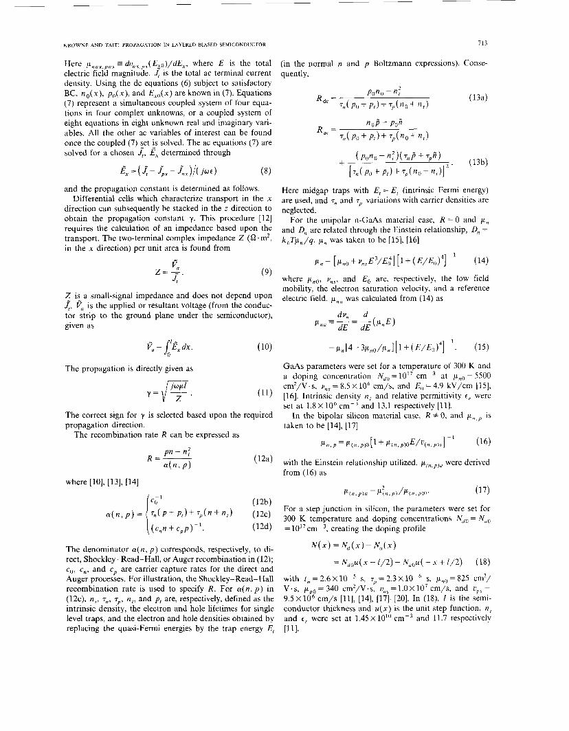
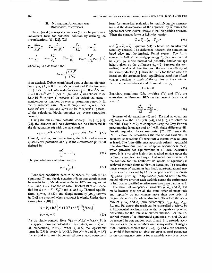
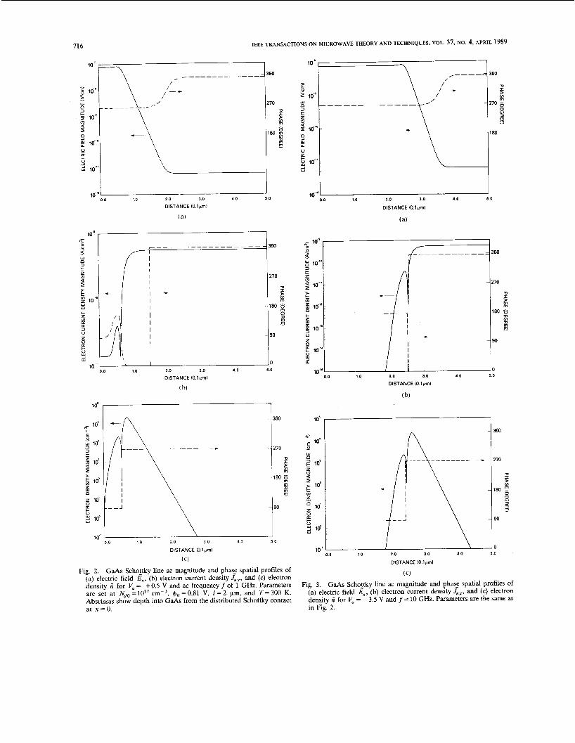
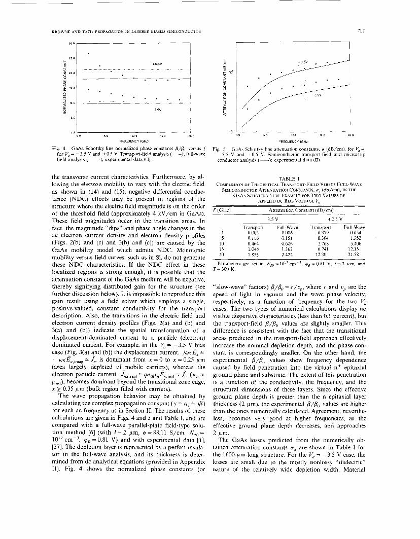
The dc simulations were carried out over an applied voltage V, range of - 3.5 V to + 0.5 V. The calculated dc electron particle currents were - 5.6 X l o p 8 A/cm2 and 13.2 A/cm2 for the -3.5 V and + O S V bias limits, respectively. The dc spatial profiles were then utilized in the ac simulations, which were run with imgressed termi- nal currents operating at frequencies f from 1 GHz to 20 GHz. Fig. 2(a)-(c) shows the magnitudes and phase angles (with respect to the terminal current) for the ac electric field the electron current density xIy, and the electron density n” respectively for a dc bias V, of + O S V and a frequency of 1 GHz. Likewise, Fig. 3(a)-(c) shows the same ac quantities, but for a dc bias V, of -3.5 V and a frequency of 10 GHz.
From these figures, it is evident that the width of the transition areas between space-charge depletion regions and bulk regions can be a large percentage of the depletion region width, and that these transition areas “penetrate” well into what would typically be categorized as the bulk region. In the Vu = + O S V bias example, the transitional zone width for the ac electric field, Fig. 2(a), is nearly 100 percent of the depletion region width, and starts at approximately x = 0.06 pm, which is the edge of the deple- tion region as calculated from the analytical expression
X d =\i24q5, - V,)/(&O)
where q5, is the built-in potential. Similarly, the transitional area begins at approximately x = 0.25 pm (edge of analyti- cally computed depletion region) and extends about 0.1 pm further into the n layer for the V, = - 3.5 V case (Fig, 3(a)). Unlike field solutions which assume a “hard,” distinct interface between the depletion region (U = 0) and the bulk region (U = constant), these “soft” transitions are more realistic and can be simulated only with a combined transport-field approach which can adequately describe
716 IEEE TRANSACTIONS ON MICROWAVE THEORY AND TECHNIQUES, VOL. 31, NO. 4, APRIL 1989
- 10 20 3.0 4.0 5.0 0 0
DISTANCE IO.lpml
( a )
'
DISTANCE lO.lprnl
(b)
360
- 270
D
R -180 g
0 m m -
7 90
\ I 00 1 0 20 3 0 4 0 5 0
DISTANCE IO.lpm)
( C )
Fig. 2. GaAs Schottky line ac magnitude and phas? spatial profiles of (a) electric field Ex, (b) electron current density .Inx, and (c) electron r l m c i t v ii for V = + O 5 V and ac freauencv f of 1 GHz. Parameters , . --- " - 1 2 . I --__l-. are set at N,,=lO" ~ m - ~ , +,=0.81 V, / = 2 pm, and T=300 K. Abscissas show depth into GaAs from the distributed Schottky contact at x = 0.
lo-'~o,o k 1.0 2.0 3.0 4.0 5.0
DISTANCE IO.lprn)
(a )
0.0 1.0 2.0 3.0 4.0 5.0
DISTANCE (0.lprnl
(C)
160
270
V
E; 180
rn 0 m rn -
90
D
Fig. 3. GaAs Schottky line ac magnitude and phas: spatial profiles of (a) electric field .Ex, (b) electron current density .Inx, and (c) electron density A for V, = - 3.5 V and f = 10 GHz. Parameters are the same as in Fig. 2.
KROWNE AND TAIT: PROPAGATION IN LAYERED BIASED SEMICONDUCTOR
+0.5V ........................................................................... 1
. . . .
30.0
25.0 c Q t- z 20.0 U
w v)
$ 1 5 0
9 a t o o z -
z 5.0
0.0 0 0 5 0 10 0 15 0 20 0
FREQUENCY IGHzI
Fig. 4. GaAs Schottky line normahzed phase constants p / p 0 versus f for Vu = - 3.5 V and +0.5 V. Transport-field analysis (-); full-wave field analysis (----); experimental data (0).
the transverse current characteristics. Furthermore, by al- lowing the electron mobility to vary with the electric field as shown in (14) and (15), negative differential conduc- tance (NDC) effects may be present in regions of the structure where the electric field magnitude is on the order of the threshold field (approximately 4 kV/cm in GaAs). These field magnitudes occur in the transition areas. In fact, the magnitude “dips” and phase angle changes in the ac electron current density and electron density profiles (Figs. 2(b) and (c) and 3(b) and (c)) are caused by the GaAs mobility model whch admits NDC. Monotonic mobility versus field curves, such as in Si, do not generate these NDC characteristics. If the NDC effect in these localized regions is strong enough, it is possible that the attenuation constant of the GaAs medium will be negative, thereby signifying distributed gain for the structure (see further discussion below). It is impossible to reproduce th s gain result using a field solver which employs a single, positive-valued, constant conductivity for the transport description. Also, the transitions in the electric field and electron current density profiles (Figs. 2(a) and (b) and 3(a) and (b)) indicate the spatial transformation of a displacement-dominated current to a particle (electron) dominated current. For example, in the V, = -3.5 V bias case (Fig. 3(a) and (b)) the displacement current, jocEx = - w ~ E , , , , , ~ = J,, is dominant from x = 0 to x = 0.25 pm (area largely depleted of I mobile carriers), whereas the electron particle current, J,,x,real = qnOpL.Ex,,,,l = 4, (p, , = pno) , becomes dominant beyond the transitional zone edge, x 2 0.35 pm (bulk region filled with carriers).
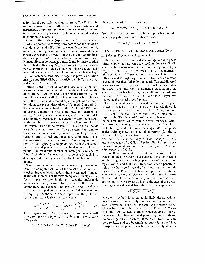
The wave propagation behavior may be obtained by calculating the complex propagation constant ( y = a, + j f l ) for each ac frequency as in Section 11. The results of these calculations are given in Figs. 4 and 5 and Table I, and are compared with a full-wave parallel-plate field-type solu- tion method [6] (with 1 = 2 pm, 0=88.11 S/cm, N d o = loL7 ~ m - ~ , + B = 0.81 V) and with experimental data [l], [27]. The depletion layer is represented by a perfect insula- tor in the full-wave analysis, and its thickness is deter- mined from dc analytical equations (provided in Appendix 11). Fig. 4 shows the normalized phase constants (or
-
$ 5 0 10 0 15 0 20 0
FREQUENCY IGHrl
717
. .
Fig. 5. GaAs Schottky line attenuation constants, a (dB/cm), for V, = ~ 3.5 V and + 0.5 V . Semiconductor transport-field and microstrip conductor analysis (-): experimental data (0).
TABLE I COMPARISON OF THEORETICAL TRANSPORT-FIELD VERSUS FULL-WAVE
SLMICONDUCTOR ATTLNUATION CONSTANTS, a, (db/cm), IN THE GAAS SCHO~TKY LINE EXAMPLE FOR Two VALUES OF
APPLIED DC BIAS VOLTAGE Vu
F (GHz) Attenuation Constant (dB/cm)
-3.5 v +0.5 V
Transport Full-Wave Transport Full-Wave 1 0.005 0.006 - 0.379 0.054 5 0.116 0.151 0.384 1.352
10 0.464 0.606 2.768 5.406 15 1.044 1.363 6.741 12.15 20 1.855 2.422 12.30 21.58
Parameters are set at N,,, = 10” cm-3, @B = 0.81 V , I = 2 pm, and T = 300 K.
“slow-wave’’ factors) P/& = c / u p , where c and up are the speed of light in vacuum and the wave phase velocity, respectively, as a function of frequency for the two V, cases. The two types of numerical calculations display no visible dispersive characteristics (less than 0.1 percent), but the transport-field p/& values are slightly smaller. This difference is consistent with the fact that the transitional areas predicted in the transport-field approach effectively increase the nominal depletion depth, and the phase con- stant is correspondingly smaller. On the other hand, the experimental f l /& values show frequency dependence caused by field penetration into the virtual n + epitaxial ground plane and substrate. The extent of this penetration is a function of the conductivity, the frequency, and the structural dimensions of these layers. Since the effective ground plane depth is greater than the n epitaxial layer thickness (2 pm), the experimental P/PO values are higher than the ones numerically calculated. Agreement, neverthe- less, becomes very good at higher frequencies, as the effective ground plane depth decreases, and approaches 2 pm.
The GaAs losses predicted from the numerically ob- tained attenuation constants a, are shown in Table I for the 1600-pm-long structure. For the V, = - 3.5 V case, the losses are small due to the mostly nonlossy “dielectric” nature of the relatively wide depletion width. Material
718 IEEE TRANSACTIONS ON MICROWAVE THEORY AND TECHNIQUES, VOL. 37, NO. 4, APRIL 1989
$ lo'*
2 I 1
losses in the Vu = + O S V case are larger for frequencies greater than 5 GHz since the depletion width is extremely narrow. For frequencies less than 5 GHz, however, NDC characteristics of the Schottky microstrip structure with applied bias of V , = + O S V are simulated by the trans- port-field method, and a very small gain is predicted. Actually, the total attenuation constant for the structure, a = a, + a=, is dominated by ohmic loss in the metallic microstrip conductor (a,.), and this loss mechanism swamps out any gain contribution from the GaAs semiconductor material (negative a,). In order to estimate this conductor loss, a microstrip computer program was utilized with the experimental p/po values providing the effective permit- tivity values (eeff) and effective ground plane spacings (&) as follows [l]:
W
3
9
t $ 1 0 ' * ~
2
and
- 270 \ \ I
-I D
P F
The thickness t of the microstrip line is 0.63 pm. The Au/Pt/Ti microstrip resistivity is taken as pAu= 2 . 4 4 ~ 1 0 - ~ Cl-cm. a,. (dB/cm) is calculated by a standard method [29]. The sum of the theoretically calculated semi- conductor and metal contributions to the loss is plotted against the actual experimental loss data in Fig. 5 for the two Vu cases. In these comparisons, the calculated loss values are smaller than the experimental ones, since the numerical simulation accounted for neither field penetra- tion into the virtual n + epitaxial ground plane and sub- strate nor other sources of experimental loss. The same frequency behavior, however, is observed. At lower fre- quencies, the approximate 0 behavior due to the metallic conduction mechanism of the strip is evident, but the semiconductor losses are seen to contribute as well at the higher frequencies, where the loss increases with frequency at a rate somewhat higher than 0. B. Transmission Line over Si Bipolar Junction
The next structure examined is a transmission line inter- connect over a Si bipolar step junction with a very small transverse dimension (3 pm). Although interconnections generally lie over passive semiconductor material, they must also pass in the vicinity of, or sometimes over, active devices which have micron and submicron feature sizes for higher speed (GHz digital and logic pulse) and denser circuits. The wave propagation behavior through these active, inhomogenously doped semiconductor regions is determined by considering the two-carrier (electron and hole) transport interaction with the electromagnetic field.
The dc simulations were carried out over an applied voltage Vu range of - 3.0 V to + 0.3 V. (The metallurgical junction is located at x = 0, and distances of 0.4 pm are shown in the figures below on both sides of this junction.) Minority carrier current densities Jnor and Jpox in, respec- tively, the left- and right-hand sides of the semiconductor
A .
n
c I I 5 io.'$ ~
I- I I g lo-" :
m
B
10-
--_ . ,--- 360 \
: s m
\ I
4
10 ') -4 0 -2 0 0 0 20 4 0
DISTANCE IO lrm)
(a)
270
360
-270 I
% - U
-180 3 rn -
\ I
-I I I I I I I I
-2.0 0.0 2.0 4.0 lo-'&
-4 0 DISTANCE IO.lrrn)
(h )
A .
10'
L
1 I I i
-2.0 0 0 2.0 4.0
DISTANCE iO.lfiml
( C l
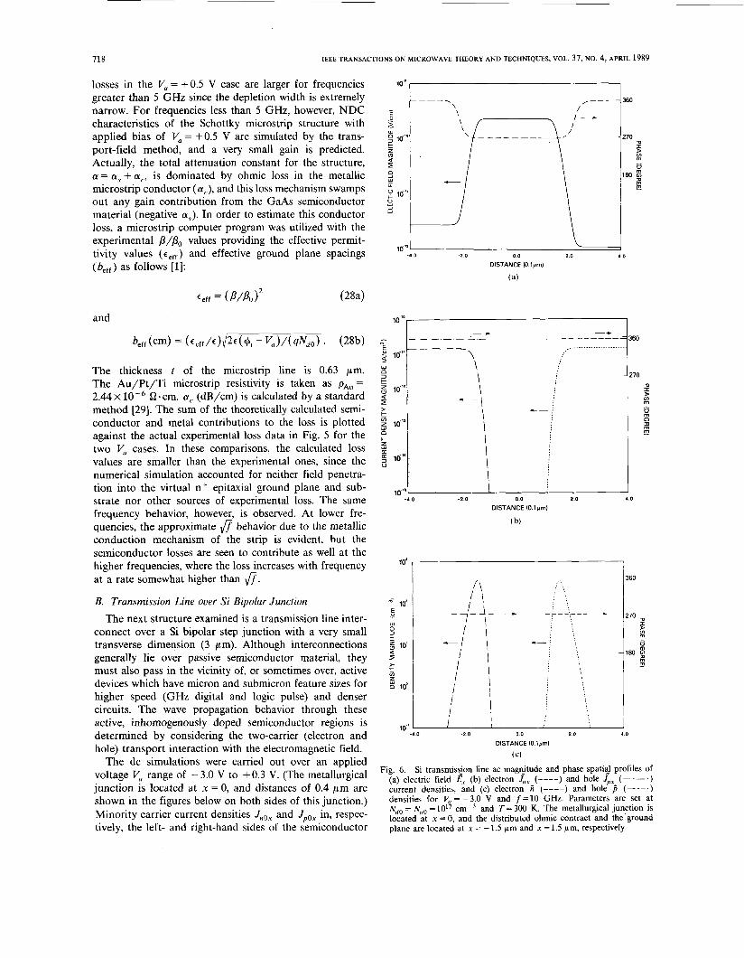
Fig. 6. Si transmissjon line ac magnjtude and phase spatia! profiles of (a) electric field E, (b) electron J,, (----) and hole J , , - ( - . - . ) current densities, and (c) electron A (----) and hole p (--.-.) densities for Vu = -3.0 V and f = l 0 GHz. Parameters are set at Ndo = No, =loL7 cm-3 and T = 300 K. The metallurgical junction is located at x = 0, and the distributed ohmic contract and the ground plane are located at x = - 1.5 pm and x = 1.5 pm, respectively.
KROWNE AND TAIT: PROPAGATION IN LAYERED BIASED SEMICONDUCTOR 719
I i , 17.4 10.' I
4 360
i 270
-2.0 0 0 2.0 4.0
DISTANCE IO.lprnl
( a )
\ \ *
i l I I I I I I I
ILO V
> F - 0 m 0
m m -
1; -4 0 -2.0 0 0 2 0 4 0
DISTANCE IO.lprn)
( b )
1 0'
DISTANCE lO.lprnl
(cl
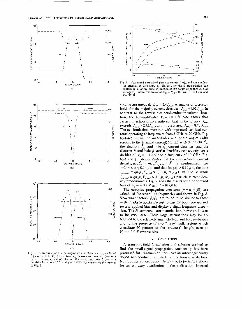
Fig. 7. Si transmisGon line ac magnitude and phase spatit1 profiles of (a) electric field E, , (b) electron J r A (----) and hole JPi (- . - .) current densities, and (c) electron 5 (----) and hole j (--.--.) densities for Vu = +0.3 V and f =10 GHz. Parameters are the same as in Fig. 7.
\- i 17.0
0 0 5 0 10 0 15 0 20 0
FREQUENCY (GHz)
Fig. 8. Calculated normalized phase constants, p/p0, and semiconduc- tor attenuation constants, a, (dB/cm), for the Si transmission line containing an abrupt bipolar junction at two values of applied dc bias voltage V,. Parameters are set at Ndo = No, =10'7cm-3, I = 3 pm, and T = 300 K.
volume are unequal, Jnox = 2.4JpOx. A smaller discrepancy holds for the majority current densities, Jnox = 1.02Jp0,. In contrast to the reverse-bias semiconductor volume situa- tion, the forward-biased Vu = 1-0.3 V case shows that carrier injection is so significant that in the p area Jnox exceeds Jpox = 2.35Jp0,, and in the n area Jpox = 0.41 Jnox.
The ac simulations were run with impressed terminal cur- rents operating at frequencies from l GHz to 20 GHz. Fig. 6(a)-(c) shows the magnitudes and phase angles (wch respect to the terminal current) for the ac electric field E,, the electron x x and hole J X current densities, and the electron fi and hole p carrier densities, respectively, for a dc bias of Vu = - 3.0 V and a frequency of 10 GHz. Fig. 6(a) and (b) demonstrates that the displacement current density, jwcl?, = -we ix , imag = J , is predominant for - - 0.14 6 x 6 0.14 pm, and - that for 1x1 z 0.14 pm, the hole
Jnx,red = qrzopnEx,red = J, ( p n = pno) particle current den- sity predominates. Fig. 7 gives the results for a dc forward bias of V, = + 0.3 V and f = 10 GHz.
The complex propagation constants ( y = a, + J/3) are calculated for several ac frequencies and shown in Fig. 8. Slow wave factors, p/p0, are found to be similar to those in the GaAs Schottky microstrip case for both forward and reverse applied bias and display a slight frequency disper- sion. The Si semiconductor material loss, however, is seen to be very large. These large attenuations may be at- tributed to the relatively small electron and hole mobilities and to the presence of two "lossy" bulk regions which constitute 90 percent of the structure's length, even at V, = -3.0 V reverse bias.
V. CONCLUSION A transport-field formulation and solution method to
find the small-signal propagation constant y has been presented for transmission lines over an inhomogeneously doped semiconductor substrate, under transverse dc bias. Net doping concentration N ( x) = N d ( x ) - Nu( x) allows for an arbitrary distribution in the x direction. Internal
Jpx.real - = 4PoPpEx,rea1 - z 4 ( ~ p z P ~ O ) or the electron
720 IEEE TRANSACTIONS ON MICROWAVE THEORY AND TECHNIQUES, VOL. 37, NO. 4, APRIL 1989
junctions and severely graded areas withm the semicon- ductor volume may be treated besides more slowly varying distributions. The transport model includes electrons and holes, recombination-generation processes, dc and ac field-dependent mobilities and diffusion constants, and boundary condition contact effects. The dispersion of the propagating wave due to doping inhomogeneity, substrate loss, and other transport effects is accounted for by the self-consistent approach used here. The dominant TM, mode method should be applicable for strip widths w 2 1 = transverse semiconductor thickness, and millimeter-wave frequencies based upon a maximum transport model fre- quency limit inversely proportional to the energy relax- ation time [30]. For GaAs, this limit is 50-100 GHz, depending upon the maximum dc electric field.
Two layered structures of interest to monolithic mi- crowave integrated circuits and hlgh-speed digital inte- grated circuits were studied. The first structure, a GaAs voltage variable phase shifter, is representative of applica- tions found in monolithic microwave integrated circuits. The second structure, a transmission line over a Si bipolar junction, is representative of applications found in high- speed digital integrated circuits. Both structures addressed the problem of present interest, i.e., the modification of propagation characteristics due to altered transport condi- tions caused by the applied dc bias. This problem is of special interest where interconnections pass into regions near or over active devices.
The solution method calculated the dc carrier densities, quasi-Fermi potentials, dc electric potential, and dc elec- tric field in order to find the correct ac carrier densities, electric field, and current densities. The propagation con- stant y was then determined from the ac information for both structures. Detailed transport variable information, as provided by the solution method, allows insight to be gained about the location of ac and dc carriers, the relative contributions of particle and displacement currents to the total ac current, and other valuable facts. This transport variable information provides insight into how the trans- port affects the calculation of y. For example, the redistri- bution of carriers in the vicinity of junctions such as the Schottky barrier in the GaAs phase shifter structure is shown to influence the propagation constant. Specifically, the y result shows that a simplified full-wave field solver, without the more detailed physical transport processes provided in our model, overestimates the wave slowing. Good agreement with experimental data is obtained for that particular example when f > 10 GHz and V, = 0.5 V.
APPENDIX I
If z-component currents are retained (except J,, = 0), then
= - w2pcEx + j w p ( xx + JX) (Ala)
d 2,??z - 4 - + y 2 E z + y - ( P - C ) dx
-- 4x yJz = - j w @ - qRuc(ii, 3; n o , p o ) dx
(Ald)
J Z = 4 P p u z ~ ~ x o ~ ~ o ~ z + 4~,(Ex0)YP. ( A m
Equations (6 ) must be solved first, subject to appropri- ate BC's, in order to provide the dc values required in (Al) which vary spatially. By Faraday's law,
Therefore the propagating wave is a TM, mode. Thus
Here k 2 = w2cp. Dropping (Ala) from (Al) and employing (A3a) allows a coupled set of nonlinear, ordinary differen- tial equations to be solved for five ac variables, from which all of the other variables may be found:
d i z dx -=[
KROWNE AND TAIT: PROPAGATION IN LAYERED BIASED SEMICONDUCTOR 721
dY - = o . d x
In (A4) f is a dummy variable eliminating the second-order spatial derivative in (Alb), and the last equation allows y to be self-consistently determ&ed to satisfy the remaining suite of equations [25]. If E, and v.E are sufficiently small so that the first two field equations in (A4) can be decoupled from the remaining five, and a small differential cell examined so that y + O , then (A4) reduce to the fundamental TM, mode case in (7).
It is possible to include y-component ac perturbations by retaining extra- eqyations such as (Ala), (Ale), and (Alg) containing Ey, Jny and Jpy variables. Such an inclu- sion creates a hybrid mode because E,(YJ,,,~;~( Exo) and aE.,/ax # 0 in (A2). In general, field-dependent mobilities will not be spatially constant, as can be seen when examin_- ing the variation of p, across a pn junction area. Thus Ey cannot be constant and TM modes are excluded.
APPENDIX I1 In order to start the dc numerical calculations, initial
values for the spatially dependent variables throughout the inhomogeneous semiconductor volume are chosen for the equilibrium solution over a selected nonuniform mesh by using the analytical expressions derived from the depletion approximation for junctions. These equilibrium formulas are provided below for the normalized variables. For the unipolar n-GaAs Schottky line case, we use
Here, X, and 6, are the normalized depletion region depth and built-in potential.
In the bipolar Si abrupt junction case, we use
j $ ( - . , > 3 - 1/25 x I - xp
J I ( - X p ) + N,(x + ZP)*/2, - xp I x I O I tj ( 2 , ) - N, (x - X,J2/2, 0 I x I x, tj(x) =
\? (x, 1 x, I x I 1 / 2
$(-yP) = -ln(lv,/ i i ,) ;$(i ,) =ln(N,/n,)
Fp=\l‘2~,N,/[ll:,(N,+N,)]
xn=/25 ,Fu/[sd(Fd + Nu)] 6, = In ( NUfid/Z:) Exo( 2) = - d $ ( X ) / d i
& ( X ) = $ p ( X ) = O J , , , ( X ) = J , , , ( X ) = O . (A6)
Here, X, and X p are the depletion region depths extending into the n and p regions, respectively, with the metallurgi- cal junction at X = 0. New trial values of the variables at applied bias voltage increments AV, can be chosen:
REFERENCES [ l ] C. M. Krowne and E. J. Cukauskas, “GaAs slow wave phase shifter
characteristics at cryogenic temperatures,” IEEE Trans. Electron Deuices, vol. ED-34, pp. 1183-1186, May 1987. V. M. Hietala, Y. R. Kwon, and K. S. Champlin, “Broadband continuously variable microwave phase shifter employing a dis- tributed Schottky contact on silicon,” Electron. Lett., vol. 23, pp. 615-677, June 1987. K. Fricke and H. L. Hartnagel, “GaAs MESFET optimization and new device applications based on wave property studies,” in IEEE MTT-S Int. Microwave Symp. Dig., June 1985, pp. 192-195. Y . Fukuoka and T. Itoh, “Field analysis of a millimeter-wave GaAs double-drift Impatt diode in the traveling-wave mode,” IEEE Trans. Microwuue Theory Tech., vol. MTT-33, pp. 216-220, Mar. 1985. H. Hasegawa, M. Furukawa, and H. Yanai, “Properties of mi- crostrip line on Si-SiO, system,” IEEE Trans. Microwave Theon. Tech., vol. MTT-19, pp. 869-881, Nov. 1971. C. M. Krowne, “Slow-wave propagation in two types of cylindrical waveguides loaded with a semiconductor,” IEEE Trans. Microwuue Theory Tech., vol. MTT-33, pp. 335-339, Apr. 1985. W. McKenzie, D. M. Barry, C. M. Snowden, and M. J. Howes, “Computer- aided design of MMIC structures,” Proc. Inst. Ekc . Eng., vol. 133, pt. H, pp. 405-410, Oct. 1986. T. -S. Mu, H. Ogawa, and T. Itoh, “Characteristics of multiconduc- tor, asymmetric, slow-wave microstrip transmission lines,” IEEE Trans. Microwave Theory Tech.. vol. MTT-34, pp. 1471-1477, Dec. 1986. W. Heinrich and H. L. Hartnagel, “Wave-theoretical analysis of signal propagation on FET electrodes,” Electron. Lett., vol. 19. pp. 65-67, Jan. 1983.
[lo] M. Kurata, Numerical Analysis for Semiconductor Devices. Lex- ington, MA.: Lexington Books, 1982.
[2]
[3]
[4]
[5]
[6]
[7]
[8]
[9]
722 IEEE TRANSACllONS ON MICROWAVE THEORY AND ‘TECHNIQUES, \’OL. 37. NO. 4. APRIL 1989
S. M. Sze, Physrs of Semiconductor Devices, 2nd ed. New York: Wiley, 1981. C. M. Krowne, “Perturbational solutions of the Boltzmann trans- port equation for n+ nn+ structures,” Proc. Inst. Elec,. Eiig., vol. 134, pt. I. pp. 93-100, June 1987. S. Selberherr. Anulysis and Simulution of Semiconductor Dei~ces. New York: Springer-Verlag, 1984. W. L. Engl, H. K. Dirks, and B. Meinenhagen, “Device modeling.” Proc. I E E E , vol. 71, pp. 10-33, Jan. 1983. W. R. Curtice. “Direct comparison of the electron-temperature model with the particle-mesh (Monte-Carlo) model for the GaAs MESFET,” IEEE Truns. Electron Devices, vol. ED-29. pp. 1942-1943, Dec. 1982. D. S. Newman, D. K. Ferry, and J. R. Sites, “Measurement and simulation of GaAs FET’s under electron-beam irradiation,” I E E E Truns. Electron Deoices, vol. ED-30. pp. 849-855, July 1983. L. M. Dang and M. Konaka, “A two-dimensional computer analy- sis of triode-like characteristics of short-channel MOSFET’s.” I E E E Truns. Electron Devices, vol. ED-27, pp. 1533-1539. Aug. 1980. J. G. Fossum and D. S. Lee, “A physical model for the dependence of carrier lifetime on doping density in nondegenerate silicon,” Solid-Stute Electron., vol. 25, pp. 741-747. Aug. 1982. F. Masszi, P. -A. Tove, K. Bohlin and H. Norde. “Computer modeling and comparison of different rectifier ( M - S , M - S - M , p-ti-n ‘ ) diodes,” IEEE Truns. Electron Devices, vol. ED-33, pp. 469-476. Apr. 1986. N. D. Arora, J. R. Hauser, and D. J. Roulston, “Electron and hole mobilities in silicon as a function of concentration and tempera- ture,” I E E E Truns. Electron Der~ices, vol. ED-29, pp. 292-295. Feb. 1982. A. DeMari, “An accurate numerical steady-state one dimensional solution of the p - n junction,” Solid-Stute Electron., vol. 11. pp. 33-58, Jan. 1968. A. DeMari, “An accurate numerical one-dimensional solution of the p - n junction under arbitrary transient conditions,” Solid-Stute Electroti., vol. 11, pp. 1021-1053, Nov. 1968. H. K. Gummel, “A sclf-consistent iterative scheme for one-dimen- sional steady state transistor calculations,” IEEE Truiis. Electroil De~ices , vol. ED-11, pp. 455-465, Oct. 1964. A. S. Grove, Physics and TechnologL. of Semiconductor Dec,ice.s. New York: Wiley. 1967. V. Pereyra, “PASVA3: An adaptive finite-difference Fortran pro- gram for first order nonlinear. ordinary boundary problems,” in Code., For Boundurir Vulue Problems in Ordinurv Differentiul Equri- t io t i s . Lecture Notes on Computer Science. R . Childs et. al.. Eds.. vol. 76. Subroutine DVCPR. International Mathematical and Statistical Libraries, Inc., Houston. TX, version 9.2. 1984. C. M. Krowne and R. E. Neidert. “Solid state monolithic variable phase shifter with operation into the millimeter wave wavelength regime,” In t . J . Infrured Millimeter WULES, vol. 7, pp. 715-728, May 1986. A. K. Sinha. T. E. Smith, M. H. Read, and J. M. Poate. “n-GaAs Schottky diodes metallized with Ti and Pt/Ti,” Solid-Srute Elec~ rron.. vol. 19, pp. 489-492, 1976. K. C. Gupta, R. Garg. and I. J. R a h l , Microstrip Lines und Slor1ine.s. Dedham. MA: Artech House, 1979 G. B. Tait and C. M. Krowne, “Efficient transferred electron device simulation method for microwave and millimeter wave CAD appli- cations.” Solid-State Electron.. vol. 30. pp. 1025-1036. Oct. 1987.
Berlin: Springer-Verlag, 1979. pp. 67-88.
Clifford M. Krowne (S’73-M’74-SM’84) at- tended the Umversity of Califorma, Rerkelev. and received the B S degree in physics from the University of Califorma, Davis. in 1970 and the M S and Ph D degrees in electrical engineering from the Umversity of Califorma, Los Angeles, in 1972 and 1975, respectirely
In 1970, he was employed in the Microelec- tronics Division of Lockheed Missiles and Space Company In 1976 he joined the technical staff of the Watluns-Johnson Companj in Palo Alto,
CA, and in 1978 he became a faculty member in the Department of Electrical Engineenng at North Carolina State University, Raleigh Dr Krowne was a 1980 ASEE Summer Faculty Fellow at the NASA Johnson Space Center, Houston, TX Since 1982, he has been uith the Electronics Science and Technology Division of the Nabal Research Laboratory. Washington, DC. studying microuaie and millimeter-wake propertie\ of active and passive solid-state device\ He is also dn Adjunct P r o f e w r of Electncal Engineenng. Universitj of Manland, College Park. M D
Dr Kroune ha\ published technical papers on \olid-state electronics. microware circuits. electromagnetics. engineering education. and applied physics He has served on the technical program conference committecs of the Antennas and Propagation Society and the Microuave Theorv and Techniques Society and has chrured sessions in the electromagnetic theory, microstrip antenna. and solid-state devlces/clrcuits areas Dr Kroune was a member of the 1987 MTT Sqmposium steering committee He is a member of Phi Kappa Phi. Tau Beta Pi, and the American Phyical Societv
ogy Division of the I his research interest modeling.
Mr. Tait is a men Society.
Gregoq B. Tait (S’88) received the B.A. degree in physics from Amherst College, Amherst, MA. in 1982 and the M.S. degree in electrical engi- neering from the University of Maryland. Col- lege Park, in 1984. He is presently working to- ward the Ph.D. degree in electrical engineering at The Johns Hopkins University. Baltimore. MD.
From 1982 to 1985, he was employed by the Fairchild Communications and Electronics Com- pany in Germantown. MD. Since 1986. he has been with the Electronics Science and Technol-
\Java1 Research Laboratory, Washington. DC. where include semiconductor device physics and device
iber of Phi Beta Kappa and the American Ph>sical