Embed Size (px)
Citation preview
Progress and prospects in nanoscale dry processes:
How can we control atomic layer reactions?
Kenji Ishikawa1*, Kazuhiro Karahashi2, Takanori Ichiki3, Jane P. Chang4, Steven M. George5,W. M. M. Kessels6, Hae June Lee7, Stefan Tinck8, Jung Hwan Um9, and Keizo Kinoshita2
1Nagoya University, Nagoya 464-8601, Japan2Osaka University, Suita, Osaka 565-0871, Japan3The University of Tokyo, Bunkyo, Tokyo 113-8656, Japan4University of California, Los Angeles (UCLA), CA 90095, U.S.A.5University of Colorado, Boulder, CO 80309, U.S.A.6Eindhoven University of Technology, 5600 MB Eindhoven, The Netherlands7Pusan National University, Busan 609-735, Republic of Korea8University of Antwerp, B-2610 Antwerpen-Wilrijk, Belgium9Samsung Electronics Co., Ltd., Yongin, Gyeonggi 449-711, Republic of Korea
*E-mail: [email protected]
Received March 10, 2017; accepted March 28, 2017; published online June 1, 2017
In this review, we discuss the progress of emerging dry processes for nanoscale fabrication. Experts in the fields of plasma processing havecontributed to addressing the increasingly challenging demands in achieving atomic-level control of material selectivity and physicochemicalreactions involving ion bombardment. The discussion encompasses major challenges shared across the plasma science and technologycommunity. Focus is placed on advances in the development of fabrication technologies for emerging materials, especially metallic andintermetallic compounds and multiferroic, and two-dimensional (2D) materials, as well as state-of-the-art techniques used in nanoscalesemiconductor manufacturing with a brief summary of future challenges. © 2017 The Japan Society of Applied Physics
1. Introduction
Transistor performance has been improved continuouslythrough the further miniaturization of features. Currently,miniaturization is continuing through newly proposed nano-scale or atomic layer control processes. The development ofnew devices, such as transistors, memories, and emergingelectrical circuit elements, is highly dependent on theestablishment of these new dry processing techniques.
Historically, lithographic pattern-transfer technology andmaterial etching processes evolved from wet to dry etchingin the late 1970s. Dramatic increases in the etching rates ofSi and Al through the use of halogen-containing gases forsputter etching were first described by Hosokawa et al.1) Thistechnique was named reactive-ion etching (RIE), and hasbeen widely used in microfabrication in the semiconductorindustry. Parallel plate electrode plasma reactors [or capaci-tively coupled plasma (CCP) reactors] have been employedfor RIE.2–4) Recognition of the importance of the ion energyand ion=neutral radical flux to the wafer surface allowedmore highly controlled etching processes through the use ofdischarges driven by two or more power sources operatedat the same or different frequencies. For example, chargedparticle and neutral radical densities can be controlled usinghigh-frequency voltages, while ion acceleration across thesheath formed over a wafer surface can be controlled throughthe low-frequency voltage.5) RIE has been proven to be anindispensable technique in fabricating ultralarge-scale inte-grated circuits (ULSIs).6,7)
With the advent of Moore’s law as the rule of thumb or asthe business model of the exponential growth in semi-conductor devices established in the 1960s, the semi-conductor industry can continue integrating devices withincreased functionality as long as processing solutions exist.8)
Around 2005, the scaling-down scenario encountered varioussevere barriers and the approach of simple miniaturization
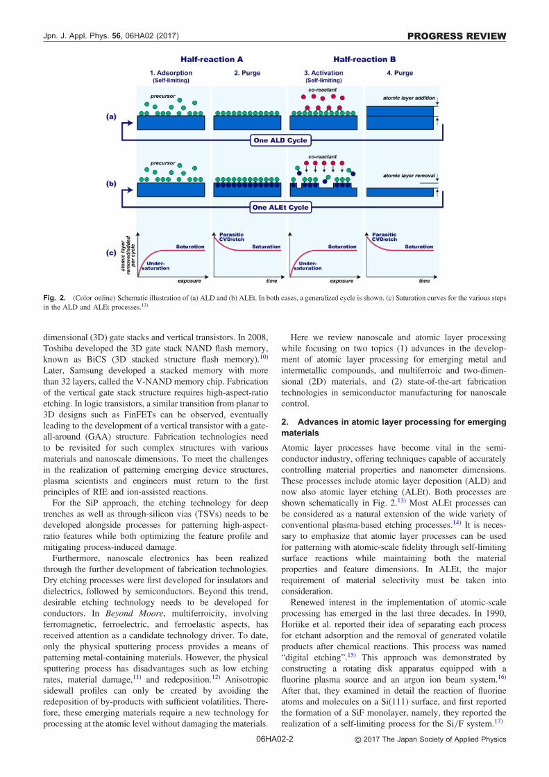
was forced to diversify. Figure 1 shows a diagram oftechnology drivers, which is based on a figure in the reportoriginally presented in the 2006 International TechnologyRoadmap for Semiconductors (ITRS).9) Continuation in the“More Moore” direction involves further miniaturization,ultimately reaching the “Beyond Moore” region, while the“More than Moore” direction explores a variety of emergingapplications other than logic and memory devices such asanalog, radio frequency (RF), passive, high-voltage (HV),high-power devices, sensors, actuators, and biochips. “Het-erogeneous integration” is a combination of the twoapproaches and is employed in creating system on chip(SoC) and system in package (SiP) solutions.
In the More Moore approach, planar device structures arebeing replaced by nonplanar device designs such as three-
Beyond Moore
More Moore
More than Moore
AnalogRF
Passives SensorsActuators
Biochips
Heterogeneous integration
System in package (SiP)System on chip (SoC)
Miniaturization
Diversification
HVPower
CMOS node [nm]:CPU,Memory,Logic
16
65
22
32
45
3. Through-Si-via (TSV) Profile control w/o damage(Cryogenic etch)
2. Emerging materials (Nanocarbons, 2D dichalcogenides, Multiferroic, etc.)
3D ideal CMOS
3D NAND flush
3. Equipment Exp. & Sim.(Gas flow & Ion trajectory)
2. Atomic layer process (ALD & ALEt)
High-aspect-ratio
Deep-RIE
Nanoscale
Fig. 1. (Color online) Technology drivers and a map of topics reviewedhere. The diagram is based on a figure originally published in the 2006 ITRSwith the addition of the reviewed topics.9) CMOS: complementary metal–oxide–semiconductor devices. CPU: central processing units.
Japanese Journal of Applied Physics 56, 06HA02 (2017)
https://doi.org/10.7567/JJAP.56.06HA02
PROGRESS REVIEW
06HA02-1 © 2017 The Japan Society of Applied Physics
dimensional (3D) gate stacks and vertical transistors. In 2008,Toshiba developed the 3D gate stack NAND flash memory,known as BiCS (3D stacked structure flash memory).10)
Later, Samsung developed a stacked memory with morethan 32 layers, called the V-NAND memory chip. Fabricationof the vertical gate stack structure requires high-aspect-ratioetching. In logic transistors, a similar transition from planar to3D designs such as FinFETs can be observed, eventuallyleading to the development of a vertical transistor with a gate-all-around (GAA) structure. Fabrication technologies needto be revisited for such complex structures with variousmaterials and nanoscale dimensions. To meet the challengesin the realization of patterning emerging device structures,plasma scientists and engineers must return to the firstprinciples of RIE and ion-assisted reactions.
For the SiP approach, the etching technology for deeptrenches as well as through-silicon vias (TSVs) needs to bedeveloped alongside processes for patterning high-aspect-ratio features while both optimizing the feature profile andmitigating process-induced damage.
Furthermore, nanoscale electronics has been realizedthrough the further development of fabrication technologies.Dry etching processes were first developed for insulators anddielectrics, followed by semiconductors. Beyond this trend,desirable etching technology needs to be developed forconductors. In Beyond Moore, multiferroicity, involvingferromagnetic, ferroelectric, and ferroelastic aspects, hasreceived attention as a candidate technology driver. To date,only the physical sputtering process provides a means ofpatterning metal-containing materials. However, the physicalsputtering process has disadvantages such as low etchingrates, material damage,11) and redeposition.12) Anisotropicsidewall profiles can only be created by avoiding theredeposition of by-products with sufficient volatilities. There-fore, these emerging materials require a new technology forprocessing at the atomic level without damaging the materials.
Here we review nanoscale and atomic layer processingwhile focusing on two topics (1) advances in the develop-ment of atomic layer processing for emerging metal andintermetallic compounds, and multiferroic and two-dimen-sional (2D) materials, and (2) state-of-the-art fabricationtechnologies in semiconductor manufacturing for nanoscalecontrol.
2. Advances in atomic layer processing for emergingmaterials
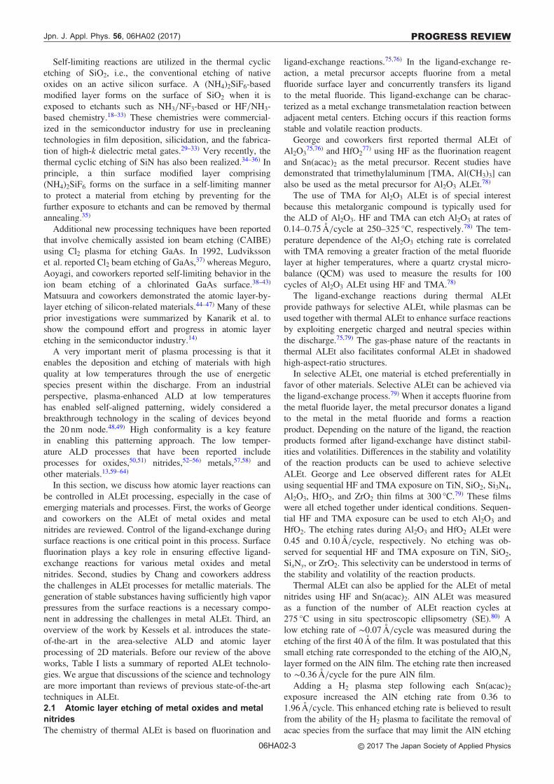
Atomic layer processes have become vital in the semi-conductor industry, offering techniques capable of accuratelycontrolling material properties and nanometer dimensions.These processes include atomic layer deposition (ALD) andnow also atomic layer etching (ALEt). Both processes areshown schematically in Fig. 2.13) Most ALEt processes canbe considered as a natural extension of the wide variety ofconventional plasma-based etching processes.14) It is neces-sary to emphasize that atomic layer processes can be usedfor patterning with atomic-scale fidelity through self-limitingsurface reactions while maintaining both the materialproperties and feature dimensions. In ALEt, the majorrequirement of material selectivity must be taken intoconsideration.
Renewed interest in the implementation of atomic-scaleprocessing has emerged in the last three decades. In 1990,Horiike et al. reported their idea of separating each processfor etchant adsorption and the removal of generated volatileproducts after chemical reactions. This process was named“digital etching”.15) This approach was demonstrated byconstructing a rotating disk apparatus equipped with afluorine plasma source and an argon ion beam system.16)
After that, they examined in detail the reaction of fluorineatoms and molecules on a Si(111) surface, and first reportedthe formation of a SiF monolayer, namely, they reported therealization of a self-limiting process for the Si=F system.17)
Fig. 2. (Color online) Schematic illustration of (a) ALD and (b) ALEt. In both cases, a generalized cycle is shown. (c) Saturation curves for the various stepsin the ALD and ALEt processes.13)
Jpn. J. Appl. Phys. 56, 06HA02 (2017) PROGRESS REVIEW
06HA02-2 © 2017 The Japan Society of Applied Physics
Self-limiting reactions are utilized in the thermal cyclicetching of SiO2, i.e., the conventional etching of nativeoxides on an active silicon surface. A (NH4)2SiF6-basedmodified layer forms on the surface of SiO2 when it isexposed to etchants such as NH3=NF3-based or HF=NH3-based chemistry.18–33) These chemistries were commercial-ized in the semiconductor industry for use in precleaningtechnologies in film deposition, silicidation, and the fabrica-tion of high-k dielectric metal gates.29–33) Very recently, thethermal cyclic etching of SiN has also been realized.34–36) Inprinciple, a thin surface modified layer comprising(NH4)2SiF6 forms on the surface in a self-limiting mannerto protect a material from etching by preventing for thefurther exposure to etchants and can be removed by thermalannealing.35)
Additional new processing techniques have been reportedthat involve chemically assisted ion beam etching (CAIBE)using Cl2 plasma for etching GaAs. In 1992, Ludvikssonet al. reported Cl2 beam etching of GaAs,37) whereas Meguro,Aoyagi, and coworkers reported self-limiting behavior in theion beam etching of a chlorinated GaAs surface.38–43)
Matsuura and coworkers demonstrated the atomic layer-by-layer etching of silicon-related materials.44–47) Many of theseprior investigations were summarized by Kanarik et al. toshow the compound effort and progress in atomic layeretching in the semiconductor industry.14)
A very important merit of plasma processing is that itenables the deposition and etching of materials with highquality at low temperatures through the use of energeticspecies present within the discharge. From an industrialperspective, plasma-enhanced ALD at low temperatureshas enabled self-aligned patterning, widely considered abreakthrough technology in the scaling of devices beyondthe 20 nm node.48,49) High conformality is a key featurein enabling this patterning approach. The low temper-ature ALD processes that have been reported includeprocesses for oxides,50,51) nitrides,52–56) metals,57,58) andother materials.13,59–64)
In this section, we discuss how atomic layer reactions canbe controlled in ALEt processing, especially in the case ofemerging materials and processes. First, the works of Georgeand coworkers on the ALEt of metal oxides and metalnitrides are reviewed. Control of the ligand-exchange duringsurface reactions is one critical point in this process. Surfacefluorination plays a key role in ensuring effective ligand-exchange reactions for various metal oxides and metalnitrides. Second, studies by Chang and coworkers addressthe challenges in ALEt processes for metallic materials. Thegeneration of stable substances having sufficiently high vaporpressures from the surface reactions is a necessary compo-nent in addressing the challenges in metal ALEt. Third, anoverview of the work by Kessels et al. introduces the state-of-the-art in the area-selective ALD and atomic layerprocessing of 2D materials. Before our review of the aboveworks, Table I lists a summary of reported ALEt technolo-gies. We argue that discussions of the science and technologyare more important than reviews of previous state-of-the-arttechniques in ALEt.2.1 Atomic layer etching of metal oxides and metalnitridesThe chemistry of thermal ALEt is based on fluorination and
ligand-exchange reactions.75,76) In the ligand-exchange re-action, a metal precursor accepts fluorine from a metalfluoride surface layer and concurrently transfers its ligandto the metal fluoride. This ligand-exchange can be charac-terized as a metal exchange transmetalation reaction betweenadjacent metal centers. Etching occurs if this reaction formsstable and volatile reaction products.
George and coworkers first reported thermal ALEt ofAl2O3
75,76) and HfO277) using HF as the fluorination reagent
and Sn(acac)2 as the metal precursor. Recent studies havedemonstrated that trimethylaluminum [TMA, Al(CH3)3] canalso be used as the metal precursor for Al2O3 ALEt.78)
The use of TMA for Al2O3 ALEt is of special interestbecause this metalorganic compound is typically used forthe ALD of Al2O3. HF and TMA can etch Al2O3 at rates of0.14–0.75Å=cycle at 250–325 °C, respectively.78) The tem-perature dependence of the Al2O3 etching rate is correlatedwith TMA removing a greater fraction of the metal fluoridelayer at higher temperatures, where a quartz crystal micro-balance (QCM) was used to measure the results for 100cycles of Al2O3 ALEt using HF and TMA.78)
The ligand-exchange reactions during thermal ALEtprovide pathways for selective ALEt, while plasmas can beused together with thermal ALEt to enhance surface reactionsby exploiting energetic charged and neutral species withinthe discharge.75,79) The gas-phase nature of the reactants inthermal ALEt also facilitates conformal ALEt in shadowedhigh-aspect-ratio structures.
In selective ALEt, one material is etched preferentially infavor of other materials. Selective ALEt can be achieved viathe ligand-exchange process.79) When it accepts fluorine fromthe metal fluoride layer, the metal precursor donates a ligandto the metal in the metal fluoride and forms a reactionproduct. Depending on the nature of the ligand, the reactionproducts formed after ligand-exchange have distinct stabil-ities and volatilities. Differences in the stability and volatilityof the reaction products can be used to achieve selectiveALEt. George and Lee observed different rates for ALEtusing sequential HF and TMA exposure on TiN, SiO2, Si3N4,Al2O3, HfO2, and ZrO2 thin films at 300 °C.79) These filmswere all etched together under identical conditions. Sequen-tial HF and TMA exposure can be used to etch Al2O3 andHfO2. The etching rates during Al2O3 and HfO2 ALEt were0.45 and 0.10Å=cycle, respectively. No etching was ob-served for sequential HF and TMA exposure on TiN, SiO2,SixNy, or ZrO2. This selectivity can be understood in terms ofthe stability and volatility of the reaction products.
Thermal ALEt can also be applied for the ALEt of metalnitrides using HF and Sn(acac)2. AlN ALEt was measuredas a function of the number of ALEt reaction cycles at275 °C using in situ spectroscopic ellipsometry (SE).80) Alow etching rate of ∼0.07Å=cycle was measured during theetching of the first 40Å of the film. It was postulated that thissmall etching rate corresponded to the etching of the AlOxNy
layer formed on the AlN film. The etching rate then increasedto ∼0.36Å=cycle for the pure AlN film.
Adding a H2 plasma step following each Sn(acac)2exposure increased the AlN etching rate from 0.36 to1.96Å=cycle. This enhanced etching rate is believed to resultfrom the ability of the H2 plasma to facilitate the removal ofacac species from the surface that may limit the AlN etching
Jpn. J. Appl. Phys. 56, 06HA02 (2017) PROGRESS REVIEW
06HA02-3 © 2017 The Japan Society of Applied Physics
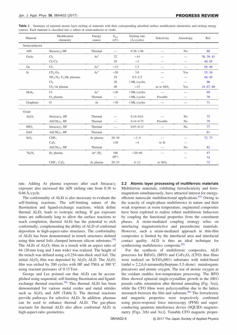
rate. Adding Ar plasma exposure after each Sn(acac)2exposure also increased the AlN etching rate from 0.36 to0.66Å=cycle.
The conformality of ALEt is also necessary to evaluate theself-limiting reactions. The self-limiting nature of thefluorination and ligand-exchange reactions, which definethermal ALEt, leads to isotropic etching. If gas exposuretimes are sufficiently long to allow the surface reactions toreach completion, thermal ALEt has the potential to etchconformally, complementing the ability of ALD of conformaldeposition in high-aspect-ratio structures. The conformalityof ALEt has been demonstrated in trench structures definedusing thin metal foils clamped between silicon substrates.79)
The ALEt of Al2O3 films in a trench with an aspect ratio of64 (30mm long and 3mm wide) was realized. The height ofthe trench was defined using a 0.254-mm-thick steel foil. Theinitial Al2O3 film was deposited by Al2O3 ALD. The Al2O3
film was etched by 200 cycles with HF and TMA at 300 °Cusing reactant pressures of 0.15 Torr.
George and Lee pointed out that ALEt can be accom-plished using sequential, self-limiting fluorination and ligand-exchange thermal reactions.79) This thermal ALEt has beendemonstrated for various metal oxides and metal nitridessuch as Al2O3 and AlN (Table I). The thermal reactionsprovide pathways for selective ALEt. In addition, plasmascan be used to enhance thermal ALEt. The gas-phasereactants for thermal ALEt also allow conformal ALEt inhigh-aspect-ratio geometries.
2.2 Atomic layer processing of multiferroic materialsMultiferroic materials, exhibiting ferroelectricity and ferro-magnetism simultaneously, have attracted interest for energy-efficient nanoscale multifunctional applications.83) Owing tothe scarcity of single-phase multiferroics in nature and theirweak responses at room temperature, engineered compositeshave been explored to realize robust multiferroic behaviorsby coupling the functional properties from the constituentphases. A strain-mediated coupling strategy relies oninterfacing magnetostrictive and piezoelectric materials.However, such a strain-mediated approach in thin-filmcomposites is limited by the interfacial area and interfacialcontact quality. ALD is thus an ideal technique forsynthesizing multiferroics composite.83)
For the synthesis of multiferroic composites, ALDprocesses for BiFeO3 (BFO) and CoFe2O4 (CFO) thin filmswere realized on SrTiO3(001) substrates with tmhd-based(tmhd = 2,2,6,6-tetramethylheptane-3,5-dione) metalorganicprecursors and atomic oxygen. The use of atomic oxygen asthe oxidant enables low-temperature processing. The BFOfilms showed epitaxial single-crystalline growth in the (001)pseudo cubic orientation after thermal annealing [Fig. 3(a)],while the CFO films were polycrystalline due to the latticemismatch between the film and substrate.84) The ferroelectricand magnetic properties were respectively confirmedusing piezo-response force microscopy (PFM) and super-conducting quantum interference device (SQUID) magneto-metry [Figs. 3(b) and 3(c)]. Tunable CFO magnetic proper-
Table I. Summary of reported atomic layer etching of materials with their corresponding adsorbed surface modification chemistries and etching energysources. Each material is classified into a subset of semiconductor or oxide.
MaterialModificationchemistry
Energysource
Eion
(eV)Etching rate(Å=cycles)
Selectivity Anisotropy Ref.
Semiconductor
AlN Sn(acac)2=HF Thermal — 0.36–1.96 — No 80
GaAs Cl2 Ar+ 22 ∼14 — — 38, 39, 41
Cl=Cl2 20 ∼3 — — 40, 65
Ge Cl2 Ar+ ∼13 1.5 — — 45, 46
Si CF4=O2, Ar+ ∼20 3.0 — Yes 15, 16
NF3=N2, F2=He plasmas 10 0.5–2.5 — — 44, 45
Cl2 20 1ML=cycles — — 66
Cl2=Ar plasma 40 ∼15 ∞ to SiO2 Yes 14, 67, 68
MoS2 Cl Ar+ <20 1ML=cycles — — 69
O2 plasma Thermal — 1ML=cycles Possible — 70
Graphene O Ar ∼30 1ML=cycles — — 71
Oxide
Al2O3 Sn(acac)2, HF Thermal — 0.14–0.61 — No 75
Al(CH3)3, HF Thermal — 0.14–0.75 Possible No 79
HfO2 Sn(acac)2, HF Thermal — 0.07–0.12 — No 77
ZnO Al(CH3)3, HF Thermal 81
SiO2 CHF3 Ar plasma 20–30 ∼1–4 — — 72, 73
C4F8 <30 ∼4 to Si —
Al(CH3)3, HF Thermal — No 82+Si3N4 H2 plasma Ar+=H2 100
(H+)∼20–60 — — 47
— 74
CHF3, C4F8 Ar plasma 20–35 4–12 to SiO2 72
Jpn. J. Appl. Phys. 56, 06HA02 (2017) PROGRESS REVIEW
06HA02-4 © 2017 The Japan Society of Applied Physics
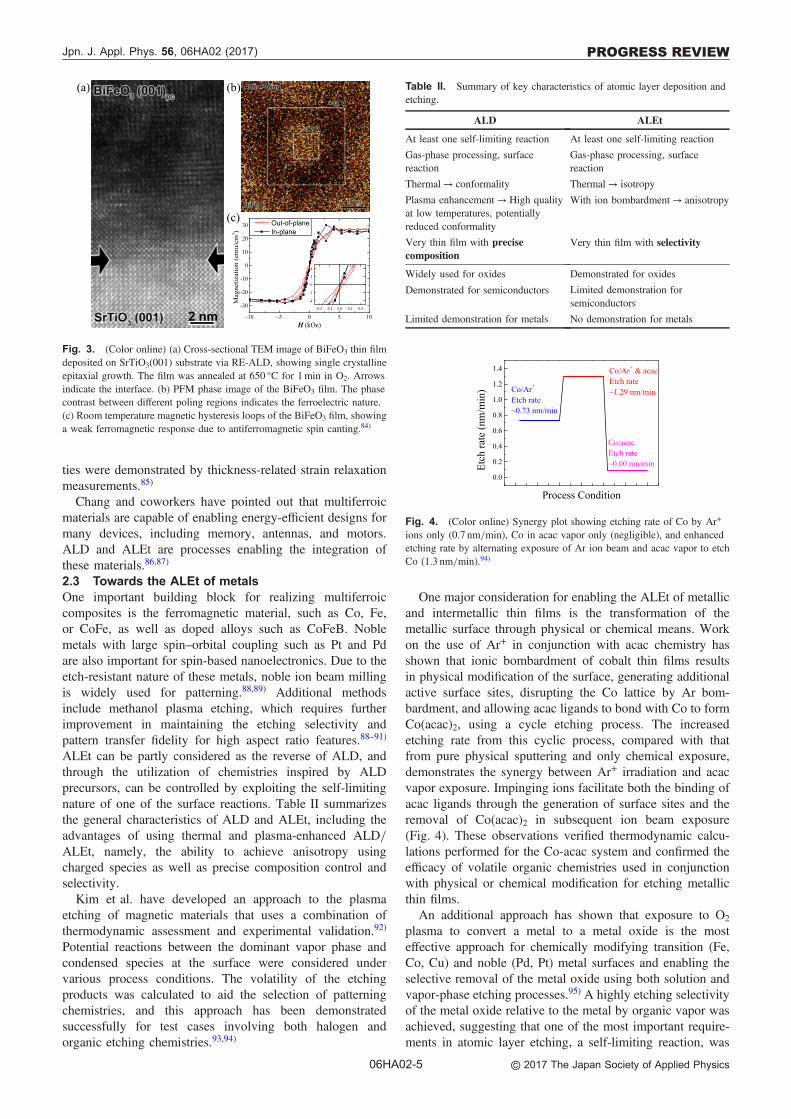
ties were demonstrated by thickness-related strain relaxationmeasurements.85)
Chang and coworkers have pointed out that multiferroicmaterials are capable of enabling energy-efficient designs formany devices, including memory, antennas, and motors.ALD and ALEt are processes enabling the integration ofthese materials.86,87)
2.3 Towards the ALEt of metalsOne important building block for realizing multiferroiccomposites is the ferromagnetic material, such as Co, Fe,or CoFe, as well as doped alloys such as CoFeB. Noblemetals with large spin–orbital coupling such as Pt and Pdare also important for spin-based nanoelectronics. Due to theetch-resistant nature of these metals, noble ion beam millingis widely used for patterning.88,89) Additional methodsinclude methanol plasma etching, which requires furtherimprovement in maintaining the etching selectivity andpattern transfer fidelity for high aspect ratio features.88–91)
ALEt can be partly considered as the reverse of ALD, andthrough the utilization of chemistries inspired by ALDprecursors, can be controlled by exploiting the self-limitingnature of one of the surface reactions. Table II summarizesthe general characteristics of ALD and ALEt, including theadvantages of using thermal and plasma-enhanced ALD=ALEt, namely, the ability to achieve anisotropy usingcharged species as well as precise composition control andselectivity.
Kim et al. have developed an approach to the plasmaetching of magnetic materials that uses a combination ofthermodynamic assessment and experimental validation.92)
Potential reactions between the dominant vapor phase andcondensed species at the surface were considered undervarious process conditions. The volatility of the etchingproducts was calculated to aid the selection of patterningchemistries, and this approach has been demonstratedsuccessfully for test cases involving both halogen andorganic etching chemistries.93,94)
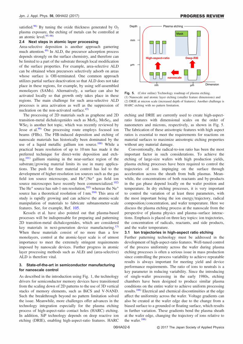
One major consideration for enabling the ALEt of metallicand intermetallic thin films is the transformation of themetallic surface through physical or chemical means. Workon the use of Ar+ in conjunction with acac chemistry hasshown that ionic bombardment of cobalt thin films resultsin physical modification of the surface, generating additionalactive surface sites, disrupting the Co lattice by Ar bom-bardment, and allowing acac ligands to bond with Co to formCo(acac)2, using a cycle etching process. The increasedetching rate from this cyclic process, compared with thatfrom pure physical sputtering and only chemical exposure,demonstrates the synergy between Ar+ irradiation and acacvapor exposure. Impinging ions facilitate both the binding ofacac ligands through the generation of surface sites and theremoval of Co(acac)2 in subsequent ion beam exposure(Fig. 4). These observations verified thermodynamic calcu-lations performed for the Co-acac system and confirmed theefficacy of volatile organic chemistries used in conjunctionwith physical or chemical modification for etching metallicthin films.
An additional approach has shown that exposure to O2
plasma to convert a metal to a metal oxide is the mosteffective approach for chemically modifying transition (Fe,Co, Cu) and noble (Pd, Pt) metal surfaces and enabling theselective removal of the metal oxide using both solution andvapor-phase etching processes.95) A highly etching selectivityof the metal oxide relative to the metal by organic vapor wasachieved, suggesting that one of the most important require-ments in atomic layer etching, a self-limiting reaction, was
-10 -5 0 5 10
-30
-20
-10
0
10
20
30
-0.4 -0.2 0.0 0.2 0.4
-4
-2
0
2
4
mc/ume(
noit azit engaM
3 )
H (kOe)
Out-of-plane In-plane
2 nm
(a) (b)
(c)
Fig. 3. (Color online) (a) Cross-sectional TEM image of BiFeO3 thin filmdeposited on SrTiO3(001) substrate via RE-ALD, showing single crystallineepitaxial growth. The film was annealed at 650 °C for 1min in O2. Arrowsindicate the interface. (b) PFM phase image of the BiFeO3 film. The phasecontrast between different poling regions indicates the ferroelectric nature.(c) Room temperature magnetic hysteresis loops of the BiFeO3 film, showinga weak ferromagnetic response due to antiferromagnetic spin canting.84)
Table II. Summary of key characteristics of atomic layer deposition andetching.
ALD ALEt
At least one self-limiting reaction At least one self-limiting reaction
Gas-phase processing, surfacereaction
Gas-phase processing, surfacereaction
Thermal→ conformality Thermal→ isotropy
Plasma enhancement→ High qualityat low temperatures, potentiallyreduced conformality
With ion bombardment→ anisotropy
Very thin film with precisecomposition
Very thin film with selectivity
Widely used for oxides Demonstrated for oxides
Demonstrated for semiconductors Limited demonstration forsemiconductors
Limited demonstration for metals No demonstration for metals
0.0
0.2
0.4
0.6
0.8
1.0
1.2
1.4
Etch
rate
(nm
/min
)Process Condition
Co/Ar+
Etch rate~0.73 nm/min
Co/Ar+ & acacEtch rate~1.29 nm/min
Co/acacEtch rate~0.00 nm/min
Fig. 4. (Color online) Synergy plot showing etching rate of Co by Ar+
ions only (0.7 nm=min), Co in acac vapor only (negligible), and enhancedetching rate by alternating exposure of Ar ion beam and acac vapor to etchCo (1.3 nm=min).94)
Jpn. J. Appl. Phys. 56, 06HA02 (2017) PROGRESS REVIEW
06HA02-5 © 2017 The Japan Society of Applied Physics
satisfied.96) By tuning the oxide thickness generated by O2
plasma exposure, the etching of metals can be controlled atan atomic level.95–98)
2.4 Next steps in atomic layer processingArea-selective deposition is another approach garneringmuch attention.49) In ALD, the precursor adsorption processdepends strongly on the surface chemistry, and therefore canbe limited to a part of the substrate through local modificationof the surface properties. For example, area-selective ALDcan be obtained when precursors selectively adsorb on areaswhose surface is OH-terminated. One common approachutilizes partial surface deactivation so that ALD does not takeplace in these regions, for example, by using self-assembledmonolayers (SAMs). Alternatively, a surface can also beactivated locally so that growth only takes place in theseregions. The main challenge for such area-selective ALDprocesses is area activation as well as the suppression ofnucleation on the non-activated surface.45)
The processing of 2D materials such as graphene and 2Dtransition-metal dichalcogenides such as MoS2, MoSe2, andWSe2 is another hot topic, which was recently reviewed byJesse et al.99) One processing route employs focused ionbeams (FIBs). The FIB-induced deposition and etching ofnanoscale materials has historically been dominated by theuse of a liquid metallic gallium ion source.100) While apractical beam resolution of up to 10 nm has made it thepreferred technique for direct-write deposition and etch-ing,101) gallium staining in the near-surface region of thesubstrate=growing material limits its use in many applica-tions. The push for finer material control has led to thedevelopment of higher-resolution ion sources such as the gasfield ion source microscope, and He+=Ne+ gas field ionsource microscopes have recently been commercialized.102)
The He+ source has sub-1-nm resolution,103) whereas the Ne+
source has a theoretical resolution of 1 nm.104) This area ofstudy is rapidly growing and can achieve the atomic-scalemanipulation of materials to fabricate subnanometer-scalefeatures. See, for example, Ref. 105.
Kessels et al. have also pointed out that plasma-basedprocesses will be indispensable for preparing and patterning2D transition-metal dichalcogenides, which are consideredkey materials in next-generation device manufacturing.13)
When these materials consist of no more than a fewmonolayers, control at the atomic-layer scale is of utmostimportance to meet the extremely stringent requirementsimposed by nanoscale devices. Further progress in atomiclayer processing methods such as ALEt and (area-selective)ALD is therefore vital.
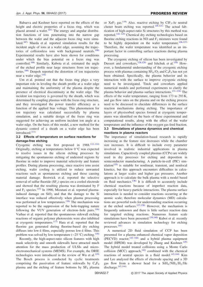
3. State-of-the-art in semiconductor manufacturingfor nanoscale control
As described in the introduction using Fig. 1, the technologydrivers for semiconductor memory devices have transitionedfrom the scaling down of 2D patterns to the use of 3D verticalstacks of memory elements, such as BiCS and V-NAND.Such the breakthrough beyond no pattern limitation solvedthe issue. Meanwhile, more challenges offer advances in thetechnology integration especially for the plasma etchingprocess of high-aspect-ratio contact holes (HARC) etching.In addition, SiP technology depends on deep reactive ionetching (DRIE), enabling high-aspect-ratio features. HARC
etching and DRIE are currently used to create high-aspect-ratio features with dimensional scales on the order ofnanometers and microns, respectively, as shown in Fig. 5.The fabrication of these anisotropic features with high aspectratios is essential to meet the requirements for reactions onmaterial surfaces to maximize anisotropic etching propertieswithout any material damage.
Conventionally, the radical-to-ion ratio has been the mostimportant factor in such considerations. To achieve theetching of large-size wafers with high production yields,plasma etching processes have been required to control thetrajectories of ions impinging on the surface throughacceleration across the sheath from bulk plasmas. Mean-while, the concentrations of both reactants and by-productsin the gas phase depend locally on the wafer position andtemperature. In dry etching processes, it is very importantto control the variation of at least three parameters, withthe most important being the ion energy=trajectory, radicalcomposition=concentration, and wafer temperature. Here wediscuss the plasma etching process at the nanoscale from theperspective of plasma physics and plasma–surface interac-tions. Emphasis is placed on three key topics: ion trajectories,the concentration of radicals, reactants, and side products,and the wafer temperature.3.1 Ion trajectories in high-aspect ratio etchingFurther patterning technology must be addressed in thedevelopment of high-aspect-ratio features. Well-tuned controlof the process uniformity across the wafer during plasmaetching processes is often a serious issue in mass productionsince controlling the process variability to achieve repeatableresults is always important for meeting yield and deviceperformance requirements. The ratio of ions to neutrals is akey parameter in reducing variability. Since the introducingof single-wafer processing in the early 1980s, etchingchambers have been designed to produce similar plasmaconditions on the entire wafer to achieve uniform processingresults.106) Electrical and chemical discontinuities at the edgeaffect the uniformity across the wafer. Voltage gradients canalso be created at the wafer edge due to the change from abiased surface to a grounded or floating surface, which resultsin further variation. These gradients bend the plasma sheathat the wafer edge, changing the trajectory of ions relative tothe wafer.106)
Depth
Dimensionμmnm
μm
mm
nanoscale
Plasma etching
Mask
Deep-RIEHigh-aspect-ratio
Fig. 5. (Color online) Technology roadmap of plasma etching.(1) Nanoscale and atomic layer etching (smaller feature dimensions) and(2) DRIE at micron scale (increased depth of features). Another challenge isHARC etching with no pattern limitation.
Jpn. J. Appl. Phys. 56, 06HA02 (2017) PROGRESS REVIEW
06HA02-6 © 2017 The Japan Society of Applied Physics
Babaeva and Kushner have reported on the effects of theheight and electric properties of a focus ring, which wasplaced around a wafer.107) The energy and angular distribu-tion functions of ions penetrating into the narrow gapbetween the wafer and the adjacent focus ring were simu-lated.107) Maeda et al. reported simulation results for theincident angle of ions at a wafer edge, assuming the trajec-tories of collisionless ions with background neutrals.108)
Experimental results have also been shown for conditionsunder which the bias potential on a focus ring wascontrolled.108) Similarly, Kubota et al. estimated the angleof the etched profile near large structures from ion trajec-tories.109) Denpoh reported the distortion of ion trajectoriesnear a wafer edge.110)
Um et al. pointed out that the focus ring plays a veryimportant role in leveling the sheath profile at a wafer edgeand maintaining the uniformity of the plasma despite thepresence of electrical discontinuity at the wafer edge. Theincident ion trajectory is governed by the sheath, which wasdetermined by coupling plasmas with the focus ring structure,and they investigated the power transfer efficiency as afunction of the applied bias voltage. This phenomenon forion trajectory was calculated successfully by plasmasimulation, and a suitable design of the focus ring wassuggested for achieving an uniform incident ion angle at awafer edge. On the basis of this model, a new method for thedynamic control of a sheath on a wafer edge has beenintroduced.111)
3.2 Effects of temperature on surface reactions fordamage-free etchingCryogenic etching was first proposed in 1988.112–114)
Originally, etching at temperatures below 0 °C was expectedto resolve issues in the silicon etching processes bymitigating the spontaneous etching of undesired regions byfluorine in order to improve material selectivity and featureprofiles. During plasma processing, since reactive ions assistetching, wafer cooling is utilized to reduce unwantedreactions such as spontaneous etching and those causingmaterial damage. Bestwick et al. reported the selectiveremoval of sulfur fluoride (SFx) species on a cooled electrodeand showed that the resulting plasma was dominated by Fand F2 species.115) In 1990, Mizutani et al. reported plasma-induced damage on SiO2 and that the damage to the Siinterface was reduced effectively when plasma processingwas performed at low temperatures.116) The mechanism wasreported to be the suppression of the hole-trapping naturefollowing the VUV generation of electron–hole pairs.116)
Varhue et al. reported that the spontaneous sidewall etchingreactions of organic polymer photoresists were also inhibitedat cryogenic temperatures.117) Hara et al. reported that thefluorine gas generated during fluorine-based dry etchingdiffuses into low-k films, especially porous low-k films. Thisproblem was solved by low-temperature (−25 °C) etching.118)
Recently, the high-aspect-ratio silicon features with highmask selectivity and smooth sidewalls have attracted muchattention for the mass production of ULSIs and micro-electromechanical systems (MEMS). For example, the DRIEtechnologies were introduced in the review of Wu et al.119)
The Bosch process is conducted by cyclic treatmentscomprising the passivation of feature sidewalls by C4F8plasma and the etching of feature bottoms by SF6 plasma
or XeF2 gas.119) Also, reactive etching by ClF3-Ar neutralcluster beam etching was reported.120,121) The actual fab-rication of high-aspect-ratio Si structures by this method wasreported.122–125) Chemical dry etching technologies based onfluorine etching reactions in NO and F2 mixtures were foundto be highly dependent on the wafer temperature.126,127)
Therefore, the wafer temperature was identified as an im-portant factor in controlling surface reactions during plasmaprocessing.
The cryogenic etching of silicon has been investigated byDussert and coworkers,128,129) and Ishchuk et al.130) How-ever, a fundamental understanding of the cryogenic etchingprocess with plasmas containing SF6=O2 and C4F8 has not yetbeen obtained. Specifically, the plasma behavior and itsinteraction with the surface to improve cryogenic etchingneed to be investigated. Tinck and coworkers appliednumerical models and performed experiments to clarify theplasma behavior and plasma–surface interactions.131–134) Theeffects of the wafer temperature, ranging from 173 to 293K,and gas flow rates on the plasma and on the etching processneed to be discussed to elucidate differences in the surfacereaction mechanisms during etching. The importance oflayers of physisorbed species formed at cryogenic temper-atures was identified on the basis of these experimental andcomputational results, along with the effect of the wafertemperature and the influence of the oxygen gas feed fraction.3.3 Simulations of plasma dynamics and chemicalreactions in plasma reactorsThe importance of simulation-based research is rapidlyincreasing as the feature size decreases while the chambersize increases. It is difficult to include every parameterinvolved in realistic industrial applications in plasmasimulations. Capacitively coupled plasmas (CCPs) are widelyused in dry processes for etching and deposition insemiconductor manufacturing. A particle-in-cell (PIC) sim-ulation135) is suitable for nonlinear, transient, and nonlocalkinetics, but this approach encounters difficulties in calcu-lations at larger scales and higher gas pressures. Anotherapproach is to calculate the bulk plasma with a model basedon fluid mechanics.136) It is difficult to accurately includechemical reactions because of imperfect reaction data,especially for heavy-particle interactions. The plasma surfaceinteraction is needed to consider reactions occurring at theatomic scale; therefore molecular dynamics (MD) calcula-tions are powerful tools for understanding reaction occurringat the etched surfaces.137,138) However, the mechanism isfrequently unknown and there is little surface reaction datafor targeted etching reactions. Numerous feature scalesimulations have been presented.139,140) Kuboi et al. recentlyreviewed advances in simulation technology for etchingprocesses.141)
A numerical 2D fluid simulation of CCP has beenpresented for a plasma enhanced chemical vapor deposition(PECVD) reactor,142–144) and a hybrid plasma equipmentmodel (HPEM) was developed by Zhang and Kushner.145)
The hybrid model treated collisions using a Monte Carlocollision (MCC) approach,142) combined with the chemicalreactions of neutral species in a fluid model.143,144) Kimand Lee analyzed the effects of electrode spacing and a 3Dgas flow from a shower head for a SiH4=NH3=H2=Hedischarge.143,144)
Jpn. J. Appl. Phys. 56, 06HA02 (2017) PROGRESS REVIEW
06HA02-7 © 2017 The Japan Society of Applied Physics
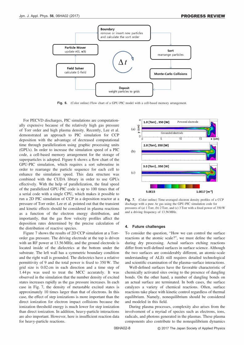
For PECVD discharges, PIC simulations are computation-ally expensive because of the relatively high gas pressureof Torr order and high plasma density. Recently, Lee et al.demonstrated an approach to PIC simulation for CCPdeposition with the advantage of decreased computationaltime through parallelization using graphic processing units(GPUs). In order to increase the simulation speed of a PICcode, a cell-based memory arrangement for the storage ofsuperparticles is adopted. Figure 6 shows a flow chart of theGPU-PIC simulation, which requires a sort subroutine inorder to rearrange the particle sequence for each cell toenhance the simulation speed. This data structure wascombined with the CUDA library in order to use GPUseffectively. With the help of parallelization, the final speedof the parallelized GPU-PIC code is up to 100 times that ofa serial code with a single CPU, which makes it possible torun a 2D PIC simulation of CCP in a deposition reactor at apressure of Torr order. Lee et al. pointed out that the transientand kinetic effects should be considered in plasma reactionsas a function of the electron energy distribution, andimportantly, that the gas flow velocity profiles affect thedeposition rates determined by the precise calculation ofthe distribution of reactive species.
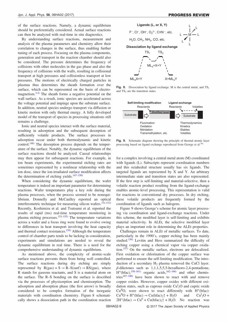
Figure 7 shows the results of 2D CCP simulation at a Torr-order gas pressure. The driving electrode at the top is drivenwith an RF power at 13.56MHz, and the ground electrode islocated inside of the dielectrics at the bottom under thesubstrate. The left wall has a symmetric boundary conditionand the right wall is grounded. The dielectrics have a relativepermittivity of 9 and the total power is fixed to 350W. Thegrid size is 0.02 cm in each direction and a time step of1.44 ps was used to treat the MCC accurately. It wasobserved in the simulation that the number density of excitedstates increases rapidly as the gas pressure increases. In eachcase in Fig. 7, the density of metastable excited states isapproximately 10 times larger than that of electrons. In thiscase, the effect of step ionizations is more important than thedirect ionization for electron impact collisions because theionization threshold energy is much lower for step ionizationthan direct ionization. In addition, heavy-particle interactionsare also important. However, here is insufficient reaction datafor heavy-particle reactions.
4. Future challenges
To consider the question, “How we can control the surfacereactions at the atomic scale?”, we must define the surfaceduring dry processing. Actual surfaces etching reactionsdiffer from well-defined surfaces in surface science. Althoughthe two surfaces are considerably different, an atomic-scaleunderstanding of ALEt still requires detailed technologicaland scientific examination of the plasma–surface interactions.
Well-defined surfaces have the favorable characteristic ofchemically activated sites owing to the presence of danglingbonds. On the other hand, a number of dangling bonds onan actual surface are terminated. In both cases, the surfacecatalyzes a variety of chemical reactions. Often, surfacereactions take place with kinetic control regardless of thermalequilibrium. Namely, nonequilibrium should be consideredand modeled in this field.
During plasma processes, complexity also arises from theinvolvement of a myriad of species such as electrons, ions,radicals, and photons generated in the plasmas. These plasmacomponents also contribute to the nonequilibrium dynamics
Fig. 6. (Color online) Flow chart of a GPU-PIC model with a cell-based memory arrangement.
(a)
(b)
(c)
Fig. 7. (Color online) Time-averaged electron density profiles of a CCPdischarge with a pure Ar gas using the GPU-PIC simulation code forpressures of (a) 1 Torr, (b) 2Torr, and (c) 3 Torr with a fixed power of 350Wand a driving frequency of 13.56MHz.
Jpn. J. Appl. Phys. 56, 06HA02 (2017) PROGRESS REVIEW
06HA02-8 © 2017 The Japan Society of Applied Physics
of the surface reactions. Namely, a dynamic equilibriumshould be preferentially considered. Actual surface reactionscan then be analyzed with real-time in situ diagnostics.
By understanding surface reactions, measurement andanalysis of the plasma parameters and chemistry allow theircorrelation to changes in the surface, thus enabling furthertuning of each process. Focusing on the plasma components,generation and transport in the reaction chamber should alsobe considered. The pressure determines the frequency ofcollisions with other molecules in the gas phase and also thefrequency of collisions with the walls, resulting in collisionaltransport at high pressures and collisionless transport at lowpressures. The motions of electrically charged particles inplasmas thus determines the sheath formation over thesurface, which can be represented on the basis of electro-magnetism.3,4) The sheath forms a negative potential on thewall surface. As a result, ionic species are accelerated acrossthe voltage potential and impinge upon the substrate surface.In addition, neutral species undergo transport via diffusion orkinetic motion with only thermal energy. A fully developedmodel of the transport of species in processing situations stillremains a challenge.
Ionic and neutral species interact with the surface material,resulting in adsorption and the subsequent desorption ofsufficiently volatile products. The surface processes inadsorption occur under both thermodynamic and kineticcontrol.146) The desorption process depends on the temper-ature of the surface. Notably, the dynamic equilibrium of thesurface reactions should be analyzed. Causal relationshipsmay then appear for subsequent reactions. For example, inion beam experiments, the experimental etching rates aresometimes represented by a nonlinear relationship with theion dose, since the ion-irradiated surface modification affectsthe determination of etching yields.147–150)
When considering the dynamic equilibrium, the wafertemperature is indeed an important parameter for determiningreactions. Wafer temperatures play a key role during theplasma processes, when the process seemed to be nonequi-librium. Donnelly and McCaulley reported an opticalinterferometric technique for measuring silicon wafers.151,152)
Recently, Koshimizu et al. and Tsutsumi et al. reported theresults of rapid (ms) real-time temperature monitoring inplasma etching processes.153–155) The temperature variationsacross a wafer and a focus ring were found to evolve owingto differences in heat transport involving the heat capacityand thermal contact resistances.154) Although the temperaturecontrol of chamber parts tends to be lacking in consideration,experiments and simulations are needed to reveal thedynamic equilibrium in real time. There is a need for thecomprehensive understanding of dynamic equilibrium.
As mentioned above, the complexity of atomic-scalesurface reactions prevents them from being well controlled.The surface reactions during dry etching are simplyrepresented by R(gas) + S → R–S(surf) → RS(gas), whereR stands for gaseous reactants, and S is a material atom onthe surface. The R–S bonding on the surface is describedvia the processes of physisorption and chemisorption. Theadsorption and absorption phase (the first arrow) is broadlyconsidered to be complex formation of the inorganicmaterials with coordination chemistry. Figure 8 schemati-cally shows a dissociation path in the coordination reaction
for a complex involving a central metal atom (M) coordinatedwith ligands (L). Subscripts represent coordination numbersand this octahedral structure usually has six ligands. Thetargeted ligands are represented by X and Y. An arbitraryintermediate state and transition states are also represented.If the first step is self-limiting and material-selective, then avolatile reaction product resulting from the ligand-exchangeenables atomic-level processing. This representation is validfor reactions in conventional dry processes. In dry etching,these volatile products are frequently formed by thecoordination of ligands such as halogens.
Figure 9 shows George’s scheme for atomic layer process-ing via coordination and ligand-exchange reactions. Underthis scheme, the modified layer is self-limiting and exhibitsmaterial selectivity. In ALEt, the selective modified layerplays an important role in determining the ALEt properties.
Challenges remain in ALEt of metallic surfaces. To date,particularly in the 1990’s, copper etching has been mainlystudied.156) Levitin and Hess summarized the difficulty ofetching copper using a chemical vapor via copper oxida-tion.157) On the metallic surface, electrons are delocalized.First oxidation or chlorination of the copper surface wasperformed to ensure the self-limiting modification. The intro-duction of a secondary H2 plasma removed the CuCl layer.β-diketones such as 1,1,1,5,5,5-hexafluoro-2,4-pentadione,H+(hfac),158–161) organic acids,162–166) and other chemis-tries167–180) have been shown to react with and removecopper oxides. However, copper oxides with different oxi-dation states, such as cuprous oxide CuI2O and cupric oxideCuIIO, were shown to react differently with H+(hfac):CuIIO + H+(hfac) → Cu(hfac)2↑ + H2O and CuI2O +2H+(hfac) → Cu0 + Cu(hfac)2↑ + H2O. No reaction was
Dissociation by ligand exchange
F−, Cl−, OH−, O22−, C≡N −, etc.
2 3 3H O, CH , NH , CO, etc.
ML5X+Y X+ML5Y
ML5+X+Y
TS1 TS2
Ligands (L, or X, Y)
M
LL
L L
L L
Fig. 8. Dissociation by ligand exchange. M is the central metal, and TS1and TS2 are the transition states.
Self-limiting modification Ligand exchange
FluorinationOxidationNitridationTransmethylation, etc.
Substrate Substrate
Volatiles
Modified layer
Reactants Reactants
ThermodynamicsKineticsStablesVolatiles
Fig. 9. Schematic diagram showing the principle of thermal atomic layerprocessing based on ligand exchange reproduced from George et al.79)
Jpn. J. Appl. Phys. 56, 06HA02 (2017) PROGRESS REVIEW
06HA02-9 © 2017 The Japan Society of Applied Physics
observed for Cu0 and H+(hfac). Therefore, if CuI is presenton the surface, both Cu0 and CuII are generated as a resultof the reaction of H+(hfac). CuII is removed by volatilizationbut Cu0 is not, eventually resulting in a buildup of Cu0 andtermination of the copper removal process.157) Thus, formetal ALEt, it is necessary to explore how to create localreaction sites with nonmetallic character, namely, those freefrom conjugated electrons and volatilization of the reactionproducts.
One approach utilizes a gas-cluster beam under acetic acidvapor to etch Pt, Ru, Ta, CoFe, and other materials.181–185)
Another approach utilizes noble ion bombardment in apreadsorption step with subsequent exposure to reactants,followed by a removal step with volatile products, as shownin Fig. 10. The resulting modified layer consists of aphysically changed material that is chemically identical tothe underlying substrate but has a different density andweaker bonding due to disruptions in the lattice, as well as anincreased number of active surface sites to which reactantscan bond and form volatile products. Kanarik et al. arguedthat ion bombardment provides energy to break the bondsunderneath the modified layer.14) The advantage of usingions is that they can be accelerated toward the wafer toprovide the benefit of directionality.186) A high ion energy isrequired due to the inefficiency in transferring the ion energyto the target bond. Energy is deposited by the impinging ionentering the subsurface region, leading to a collision cascadein the substrate material.14,186) A similar approach has beendemonstrated using noble ion beam irradiation to physicallymodify preadsorption metal surfaces and remove volatileetching products with subsequent ion exposure.94) In an effortto enable higher etching rates and achieve additionalselectivity for the dry etching of metallic thin films, reactiveoxygen plasmas have also been shown to be effective for thedirectional chemical modification of transition and noblemetals through the generation of a thin metal oxide surfacelayer upon the application of a bias voltage to the substrate.Chen et al. demonstrated the chemical contrast producedusing reactive ion bombardment with the subsequent deliveryof vapor-phase organics to the modified surface, resulting inan anisotropic and self-limiting etching process capable ofachieving greater selectivity to the underlying metal.96)
A dilemma occurs in self-limiting modifications, and aproblem is that stable by-products at room temperature tendto be nonvolatile and vice versa. In brief, the volatilities ofthe etching by-products are determined by the chemicalnature of the bonding when forming the solid phase, whichin turn depends on molecular weights, intermolecular forces,and so forth. Also, chemical bonds are the origin of the
stability of products (Fig. 11). Similarly to the complexformation of metal-ligand systems, electron donation plays animportant role in resolving this dilemma.
In plasma processes, the reactive species in the surfacereactions can be utilized, i.e., kinetic control schemes. Forinstance, atomic species react and etch spontaneously in thecase of etching bare aluminum with chlorine and alsotungsten with fluorine.187) Note that the stable solid by-products at room temperature tend to be redeposited on othersurfaces. Ion-assisted reactions have solved the redepositionproblem. The etching of metals also has the problem of theredeposition of etching by-products.12,188–197)
In self-limiting formation, another difficulty arises forintermetallic compounds or alloys such as CoFe, NiFe, CrFe,and PtMn. Simply, in etching processes for compounds suchas high-k materials, dichalcogenides, GaAs, GaP, and GaN, itis difficult to maintain the surface stoichiometry during andafter the etching. The stoichiometric changes arise fromdifferences in the volatilities of the etching by-products. Forexample, here are different vapor pressures for metalchlorides such as AlCl3, GaCl3, and NCl3 in AlGaN etchingat temperatures around room temperature. Since the vaporpressures depend on temperature, the etching reactiontemperatures should be taken into consideration. Thevolatilities of etching by-products in the GaN etchingprocesses have been discussed in terms of surface rough-ness.198–201) Self-limiting chlorination and removal of themodified layer by ion irradiation have been utilized. Ohbaet al. reported the formation of surface roughness on AlGaNin cyclic etching involving Cl2 plasma exposure and Ar ionbombardment.202) We point out that the atomic-level-controlof surface reactions will be required for the etching ofintermetallic compounds and alloys.
Additional examples of directional ALEt with ion bom-bardment are the self-limiting deposition of thin fluorocarbonfilm and their removal with ion bombardment. The
Self-limiting modification Removal of products
Substrate Substrate
Volatiles
Modified layer
Reactantsion bombarded
Ion bombardment
(Redeposition)
Fig. 10. Schematic diagram detailing implementation of directional ALEtthrough the use of ion bombardment utilizing a two-step process comprisingof (1) a modification step generated by ionic bombardment with a subsequentreaction and (2) a removal step wherein impinging ions facilitate the selectiveremoval of etching products to regenerate the original surface.
Removal of products
Substrate
Volatiles
Energy
M
LL
L L
L L
Stability
Volatility
M L
M X
M X+ −
Covalent bond
Coordinate bond
Ionic bond
ML
L
L
L
Substrate
Ion bombardmentSurface modification
Intermolecular forces- dispersion- dipole-dipole- H-bonding- molecular weight
Thermodynamic and kinetic control
Redeposition- unstable- low volatility
Fig. 11. Atomic chemical engineering in product formation in ALEt. Thevolatility and stability of the products may correlate with each other. This isbriefly explained in the main text in terms of intermolecular forces andchemical bonds.
Jpn. J. Appl. Phys. 56, 06HA02 (2017) PROGRESS REVIEW
06HA02-10 © 2017 The Japan Society of Applied Physics
fluorocarbon film thickness depends on the underlyingsurface material. For example, thinner films were depositedand higher etching rates were observed for silicon oxides andnitrides, while thicker films and lower etching rates wereobserved for silicon surfaces.203,204)
For the case of metal ALEt, low energy ion bombardmentis useful in the self-limiting formation of a ligand-exchangelayer. In Fig. 11, the ion bombardment may play two roles inALEt. One is the removal of products in the self-limitingmodified layer. The other is the pretreatment in which anactive surface is formed in a self-limiting manner on thesurface. The active surface provides high reactivity withreactants to form the modified layer because the isolatedmetal atoms may enable ligand coordination, allowingchelating products centered around the metal atom to beused for etching. The development of revolutionary methodsis needed to meet the challenges described in this section.
5. Conclusions
We have discussed the advances in fabrication technologiesin atomic layer processing for emerging materials and thestate-of-the-art in plasma etching for industrial applications tosemiconductors. We reviewed atomic layer processing fromthe perspective of physicochemical reactions and equipmentparameter control in terms of ion trajectories and gas-flowvelocity distributions in reactor chambers. The reviewedmatter includes an outline of major challenges in futureresearch on the atomic layer fidelity of dry processes. Wehave addressed parameters related to the discharge speciesand wafer temperature that should be diagnosed using real-time in situ methods since dry etching processes exist instates of dynamic equilibrium. The major challenges must beaddressed using complementary experimental and computa-tional approaches.
Acknowledgements
The authors would like to thank Drs. Masanobu Honda,Miyako Matsui, Tomohiro Okumura, Tetsuya Tatsumi,Satoshi Hamaguchi, Hiroto Ohtake, Yoshinobu Ohya,Kazunori Shinoda, Masaru Izawa, Hisataka Hayashi, ToshioHayashi, Makoto Sekine, and Masaru Hori, and all membersof the Program and Publication Committee of the 38thInternational Symposium on Dry Process 2016 held inSapporo, Japan, as well as Nicholas Altieri and Jeffrey Changat UCLA for proofreading and providing feedback on themanuscript.
1) N. Hosokawa, R. Matsuzaki, and T. Asamaki, Jpn. J. Appl. Phys. 13, 435(1974).
2) H. Abe, M. Yoneda, and N. Fujiwara, Jpn. J. Appl. Phys. 47, 1435 (2008).3) M. Lieberman and A. J. Lichtenberg, Principles of Plasma Discharges and
Materials Processing (Wiley, New York, 2005) 2nd ed.4) P. Charbert and N. Braithwaite, Physics of Radio-Frequency Plasmas
(Cambridge University Press, Cambridge, U.K., 2012).5) K. Nojiri, Dry Etching Technology for Semiconductors (Springer,
Heidelberg, 2015).6) M. Sekine, Appl. Surf. Sci. 192, 270 (2002).7) T. Tatsumi, M. Matsui, M. Okigawa, and M. Sekine, J. Vac. Sci. Technol.
B 18, 1897 (2000).8) M. M. Waldrop, Nature 530, 144 (2016).9) 2015 International Roadmap for Semiconductors (ITRS) 2.0.
10) H. Tanaka, M. Kido, K. Yahashi, M. Oomura, R. Katsumata, M. Kito, Y.Fukuzumi, M. Sato, Y. Nagata, Y. Matsuoka, Y. Iwata, H. Aochi, and A.
Nitayama, Proc. VLSI Tech. Dig., 2007, p. 14.11) K. Eriguchi, Jpn. J. Appl. Phys. 56, 06HA01 (2017).12) H. Ohtake, S. Samukawa, H. Oikawa, and Y. Nashimoto, Jpn. J. Appl.
Phys. 37, 2311 (1998).13) T. Faraz, F. Roozeboom, H. C. M. Knoops, and W. M. M. Kessels, ECS J.
Solid State Sci. Technol. 4, N5023 (2015).14) K. J. Kanarik, T. Lill, E. A. Hudson, S. Sriraman, S. Tan, J. Marks, V.
Vahedi, and R. A. Gottscho, J. Vac. Sci. Technol. A 33, 020802 (2015).15) Y. Horiike, T. Tanaka, M. Nakano, S. Iseda, H. Sakaue, A. Nagata, H.
Shindo, S. Miyazaki, and M. Hirose, J. Vac. Sci. Technol. A 8, 1844(1990).
16) H. Sakaue, S. Iseda, K. Asami, J. Yamamoto, M. Hirose, and Y. Horiike,Jpn. J. Appl. Phys. 29, 2648 (1990).
17) Y. Morikawa, K. Kubota, H. Ogawa, T. Ichiki, A. Tachibana, S. Fujimura,and Y. Horiike, J. Vac. Sci. Technol. A 16, 345 (1998).
18) H. Nishino, N. Hayasaka, and H. Okano, J. Appl. Phys. 74, 1345 (1993).19) J. Kikuchi, S. Fujimura, M. Suzuki, and H. Yano, Jpn. J. Appl. Phys. 32,
3120 (1993).20) J. Kikuchi, M. Iga, H. Ogawa, S. Fujimura, and H. Yano, Jpn. J. Appl.
Phys. 33, 2207 (1994).21) J. Kikuchi, M. Nagasaka, S. Fujimura, and H. Yano, Jpn. J. Appl. Phys. 35,
1022 (1996).22) M. T. Suzuki, J. Kikuchi, M. Nagasaka, and S. Fujimura, MRS Proc. 477,
167 (1997).23) H. Ogawa, T. Arai, M. Yanagisawa, T. Ichiki, and Y. Horiike, Jpn. J. Appl.
Phys. 41, 5349 (2002).24) T. Hayashi, K. Ishikawa, M. Sekine, M. Hori, A. Kono, and K. Suu, Jpn. J.
Appl. Phys. 51, 016201 (2012).25) T. Hayashi, K. Ishikawa, M. Sekine, M. Hori, A. Kono, and K. Suu, Jpn. J.
Appl. Phys. 51, 026505 (2012).26) T. Hayashi, J. Nanomed. Nanotechnol. S15, 1 (2013).27) N. Posseme, A. Ah-Leung, O. Pollet, C. Arvet, and M. Garcia-Barros,
J. Vac. Sci. Technol. A 34, 061301 (2016).28) T. S. Cho, Q. Han, D. Yang, S. Park, D. Lubomirsky, and S.
Venkataraman, Jpn. J. Appl. Phys. 55, 056201 (2016).29) W. C. Natzle, D. Horak, S. Deshpande, C.-F. Yu, J. C. Liu, R. W. Mann,
B. Doris, H. Hanafi, J. Brown, A. Sekiguchi, M. Tomoyasu, A. Yamashita,D. Prager, M. Funk, P. Cottrell, F. Higuchi, H. Takahashi, M. Sendelbach,E. Solecky, W. Yan, L. Tsou, Q. Yang, J. P. Norum, and S. S. Iyer, Proc.IEEE Advanced Semiconductor Manufacturing Conf. (ASMC ’04), 2004,p. 61.
30) K. Tapily, S. Consiglio, R. D. Clark, R. Vasic, C. S. Wajda, J. Jordan-Sweet, G. J. Leusink, and A. C. Diebold, ECS J. Solid State Sci. Technol.4, N1 (2015).
31) J. Lei, S.-E. Phan, X. Lu, C.-T. Kao, K. Lavu, K. Moraes, K. Tanaka, B.Wood, B. Ninan, and S. Gandikota, Proc. IEEE Int. Symp. SemiconductorManufacturing (ISSM 2006), 2006, p. 393.
32) R. Yang, N. Su, P. Bonfanti, J. Nie, J. Ning, and T. T. Li, J. Vac. Sci.Technol. B 28, 56 (2010).
33) K.-F. Lo, F.-H. Hsu, X.-G. Lin, H.-J. Lee, N.-T. Lian, T. Yang, and K.-C.Chen, Proc. IEEE Advanced Semiconductor Manufacturing Conf. (ASMC’15), 2015, p. 309.
34) K. Shinoda, M. Izawa, T. Kanekiyo, K. Ishikawa, and M. Hori, Appl.Phys. Express 9, 106201 (2016).
35) K. Shinoda, N. Miyoshi, H. Kobayashi, M. Miura, M. Kurihara, K. Maeda,N. Negishi, Y. Sonoda, M. Tanaka, N. Yasui, M. Izawa, Y. Ishii, K.Okuma, T. Saldana, J. Manos, K. Ishikawa, and M. Hori, J. Phys. D 50,016201 (2012).
36) N. Miyoshi, H. Kobayashi, K. Shinoda, M. Kurihara, T. Watanabe, Y.Kouzuma, K. Yokogawa, S. Sakai, and M. Izawa, Jpn. J. Appl. Phys. 56,06HB01 (2017).
37) A. Ludviksson, M. Xu, and R. M. Mratin, Surf. Sci. 277, 282 (1992).38) T. Meguro, M. Hamagaki, S. Modaressi, T. Hara, Y. Aoyagi, M. Ishii, and
Y. Yamamoto, Appl. Phys. Lett. 56, 1552 (1990).39) Y. Aoyagi, K. Shinmura, K. Kawasaki, T. Tanaka, K. Gamo, S. Namba,
and I. Nakamoto, Appl. Phys. Lett. 60, 968 (1992).40) M. Ishii, T. Meguro, H. Kodama, Y. Yamamoto, and Y. Aoyagi, Jpn. J.
Appl. Phys. 31, 2212 (1992).41) T. Meguro, M. Ishii, K. Kodama, Y. Yamamoto, K. Gamo, and Y. Aoyagi,
Thin Solid Films 225, 136 (1993).42) M. Ishii, T. Meguro, K. Gamo, T. Sugano, and Y. Aoyagi, Jpn. J. Appl.
Phys. 32, 6178 (1993).43) T. Meguro, M. Ishii, T. Sugano, K. Gamo, and Y. Aoyagi, Appl. Surf. Sci.
82–83, 193 (1994).44) T. Matsuura, H. Uetake, T. Ohmi, J. Murota, K. Fukuda, N. Mikoshiba, T.
Kawashima, and Y. Yamashita, Appl. Phys. Lett. 56, 1339 (1990).45) T. Matsuura, J. Murota, Y. Sawada, and T. Ohmi, Appl. Phys. Lett. 63,
Jpn. J. Appl. Phys. 56, 06HA02 (2017) PROGRESS REVIEW
06HA02-11 © 2017 The Japan Society of Applied Physics
2803 (1993).46) T. Sugiyama, T. Matsuura, and J. Murota, Appl. Surf. Sci. 112, 187 (1997).47) T. Matsuura, Y. Honda, and J. Murota, Appl. Phys. Lett. 74, 3573 (1999).48) B. Degroote, R. Rooyackers, T. Vandeweyer, N. Collaert, W. Boullart, E.
Kunnen, D. Shamiryan, J. Wouters, J. Van Puymbroeck, A. Dixit, and M.Jurczak, Microelectron. Eng. 84, 609 (2007).
49) A. J. M. Mackus, A. A. Bol, and W. M. M. Kessels, Nanoscale 6, 10941(2014).
50) S. E. Potts, W. Keuning, E. Langereis, G. Dingemans, M. C. M.van de Sanden, and W. M. M. Kessels, J. Electrochem. Soc. 157, P66(2010).
51) S. E. Potts, H. B. Profijt, R. Roelofs, and W. M. M. Kessels, Chem. VaporDeposition 19, 125 (2013).
52) S. B. S. Heil, E. Langereis, F. Roozeboom, M. C. M. van de Sanden, andW. M. M. Kessels, J. Electrochem. Soc. 153, G956 (2006).
53) E. Langereis, H. C. M. Knoops, A. J. M. Mackus, F. Roozeboom,M. C. M. van de Sanden, and W. M. M. Kessels, J. Appl. Phys. 102,083517 (2007).
54) H. C. M. Knoops, E. M. J. Braeken, K. de Peuter, S. E. Potts, S. Haukka,V. Pore, and W. M. M. Kessels, ACS Appl. Mater. Interfaces 7, 19857(2015).
55) H. C. M. Knoops, K. de Peuter, and W. M. M. Kessels, Appl. Phys. Lett.107, 014102 (2015).
56) Y. Lu, A. Kobayashi, H. Kondo, K. Ishikawa, M. Sekine, and M. Hori,Jpn. J. Appl. Phys. 53, 010305 (2014).
57) A. J. M. Mackus, D. Garcia-Alonso, H. C. M. Knoops, A. A. Bol, andW. M. M. Kessels, Chem. Mater. 25, 1769 (2013).
58) M. J. Weber, A. J. M. Mackus, M. A. Verheijen, V. Longo, A. A. Bol, andW. M. M. Kessels, J. Phys. Chem. C 118, 8702 (2014).
59) H. B. Profijt, S. E. Potts, M. C. M. van de Sanden, and W. M. M. Kessels,J. Vac. Sci. Technol. A 29, 050801 (2011).
60) F. Koehler, D. H. Triyoso, I. Hussain, B. Antonioli, and K. Hempel, Phys.Status Solidi C 11, 73 (2014).
61) C. K. Ande, H. C. M. Knoops, K. de Peuter, M. van Drunen, S. D. Elliott,and W. M. M. Kessels, J. Phys. Chem. Lett. 6, 3610 (2015).
62) H. B. Profijt, P. Kudlacek, M. C. M. van de Sanden, and W. M. M.Kessels, J. Electrochem. Soc. 158, G88 (2011).
63) H. B. Profijt, M. C. M. van de Sanden, and W. M. M. Kessels,Electrochem. Solid-State Lett. 15, G1 (2012).
64) H. B. Profijt, M. C. M. van de Sanden, and W. M. M. Kessels, J. Vac. Sci.Technol. A 31, 01A106 (2013).
65) K. K. Ko and S. W. Pang, J. Vac. Sci. Technol. B 11, 2275 (1993).66) S. D. Athavale and D. J. Economou, J. Vac. Sci. Technol. B 14, 3702
(1996).67) B. J. Kim, S. H. Chung, and S. M. Cho, Appl. Surf. Sci. 187, 124 (2002).68) A. Agarwal and M. J. Kushner, J. Vac. Sci. Technol. A 27, 37 (2009).69) T. Lin, B. Kang, M. Jeon, C. Huffman, J. Jeon, S. Lee, W. Han, J. Lee, S.
Lee, and G. Y. Yeom, ACS Appl. Mater. Interfaces 7, 15892 (2015).70) H. Zhu, X. Y. Ain, L. X. Cheng, A. Azcatl, J. Kim, and R. M. Wallace,
ACS Appl. Mater. Interfaces 8, 19119 (2016).71) W. S. Lim, Y. Y. Kim, H. Kim, S. Jang, N. Kwon, B. J. Park, J. H. Ahn, I.
Chung, B. H. Hong, and G. Y. Yeom, Carbon 50, 429 (2012).72) D. Metzler, R. L. Bruce, S. Engelmann, E. A. Joseph, and G. S. Oehrlein,
J. Vac. Sci. Technol. A 32, 020603 (2014).73) D. Metzler, C. Li, S. Engelmann, R. L. Bruce, E. A. Joseph, and G. S.
Oehrlein, J. Vac. Sci. Technol. A 34, 01B101 (2016).74) N. Posseme, O. Pollet, and B. S. Barnola, Appl. Phys. Lett. 105, 051605
(2014).75) Y. Lee and S. M. George, ACS Nano 9, 2061 (2015).76) Y. Lee, J. W. DuMont, and S. M. George, Chem. Mater. 27, 3648 (2015).77) Y. Lee, J. W. DuMont, and S. M. George, ECS J. Solid State Sci. Technol.
4, N5013 (2015).78) Y. Lee, J. W. DuMont, and S. M. George, Chem. Mater. 28, 2994 (2016).79) S. M. George and Y. Lee, ACS Nano 10, 4889 (2016).80) N. R. Johnson, H. Sun, K. Sharma, and S. M. George, J. Vac. Sci. Technol.
A 34, 050603 (2016).81) D. R. Zywotko and S. M. George, Chem. Mater. 29, 1183 (2017).82) J. W. DuMont, A. E. Marquardt, A. M. Cano, and S. M. George, ACS
Appl. Mater. Interfaces 9, 10296 (2017).83) K. L. Wang and P. K. Amiri, Spin 2, 1250009 (2012).84) C. D. Pham, J. Chang, M. A. Zurbuchen, and J. P. Chang, Chem. Mater.
27, 7282 (2015).85) J. Chang and J. P. Chang, to be published in J. Phys. D: Appl. Phys. (2017).86) D. Chien, X. Li, K. Wong, M. A. Zurbuchen, S. Robbennolt, G. Yu, S.
Tolbert, N. Kioussis, P. K. Amiri, K. L. Wang, and J. P. Chang, Appl.Phys. Lett. 108, 112402 (2016).
87) X. Li, K. Fitzell, D. Wu, C. T. Karaba, A. Buditama, G. Yu, K. L. Wong,
N. Altieri, C. Grezes, N. Kioussis, S. Tolbert, Z. Zhang, J. P. Chang, P. K.Amiri, and K. L. Wang, Appl. Phys. Lett. 110, 052401 (2017).
88) K. Kinoshita, H. Utsumi, K. Suemitsu, H. Hada, and T. Sugibayashi, Jpn.J. Appl. Phys. 49, 08JB02 (2010).
89) K. Kinoshita, H. Honjo, S. Fukami, H. Sato, K. Mizunuma, K. Tokutome,M. Murahata, S. Ikeda, S. Miura, N. Kasai, and H. Ohno, Jpn. J. Appl.Phys. 53, 103001 (2014).
90) K. Kinoshita, T. Yamamoto, H. Honjo, N. Kasai, S. Ikeda, and H. Ohno,Jpn. J. Appl. Phys. 51, 08HA01 (2012).
91) K. Kinoshita, H. Honjo, S. Fukami, R. Nebashi, K. Tokutome, M.Murahata, S. Miura, N. Kasai, S. Ikeda, and H. Ohno, Jpn. J. Appl. Phys.53, 03DF03 (2014).
92) T. Kim, J. K.-C. Chen, and J. P. Chang, J. Vac. Sci. Technol. A 32, 041305(2014).
93) T. Kim, Y. Kim, J. K.-C. Chen, and J. P. Chang, J. Vac. Sci. Technol. A33, 021308 (2015).
94) J. K.-C. Chen, T. Kim, N. D. Altieri, E. Chen, and J. P. Chang, J. Vac. Sci.Technol. A 35, 031304 (2017).
95) J. K.-C. Chen, N. D. Altieri, T. Kim, T. Lill, M. Shen, and J. P. Chang,J. Vac. Sci. Technol. A 35, 05C304 (2017).
96) J. K.-C. Chen, N. D. Altieri, T. Kim, E. Chen, T. Lill, M. Shen, and J. P.Chang, J. Vac. Sci. Technol. A 35, 05C305 (2017).
97) J. K.-C. Chen, T. Kim, and J. P. Chang, ECS Trans. 75 [33], 1 (2017).98) D. Chien, A. N. Buditama, L. T. Schelhas, H. Y. Kang, S. Robbennolt,
J. P. Chang, and S. H. Tolbert, Appl. Phys. Lett. 109, 112904 (2016).99) S. Jesse, A. Y. Borisevich, J. D. Fowlkes, A. R. Lupini, P. D. Rack, R. R.
Unocic, B. G. Sumpter, S. V. Kalinin, A. Belianinov, and O. S.Ovchinnikova, ACS Nano 10, 5600 (2016).
100) F. A. Stevie, L. Giannuzzi, and B. Prenitzer, The Focused Ion BeamInstrument. Introduction to Focused Ion Beams (Springer, Heidelberg,2005) p. 1.
101) J. Gierak, A. Septier, and C. Vieu, Nucl. Instrum. Methods Phys. Res.,Sect. A 427, 91 (1999).
102) N. P. Economou, J. A. Notte, and W. B. Thompson, Scanning 34, 83(2012).
103) B. Ward, J. A. Notte, and N. Economou, J. Vac. Sci. Technol. B 24, 2871(2006).
104) F. Rahman, S. McVey, L. Farkas, J. A. Notte, S. Tan, and R. H.Livengood, Scanning 34, 129 (2012).
105) N. F. W. Thissen, R. J. H. Vervuurt, A. C. M. Mackus, J. L. L. Mulders,J. W. Weber, W. M. M. Kessels, and A. A. Bol, 2D Mater. 4, 025046(2017).
106) S. Hwang and K. Kanarik, Solid State Technol. 59 [5], 16 (2016).107) N. Y. Babaeva and M. J. Kushner, J. Phys. D 41, 062004 (2008).108) K. Maeda, K. Yokogawa, T. Ichino, T. Tamura, K. Hirozane, T. Kanekiyo,
and M. Izawa, Proc. 31st Int. Symp. Dry Process, 2009, p. 257.109) T. Kubota, H. Ohtake, R. Araki, Y. Yanagisawa, T. Iwasaki, K. Ono, K.
Miwa, and S. Samukawa, J. Phys. D 46, 415203 (2013).110) K. Denpoh, Jpn. J. Appl. Phys. 53, 080304 (2014).111) J. H. Um, T. K. Kang, H.-J. Park, and T.-Y. Yoon, Proc. 38th Int. Symp.
Dry Process, 2016, F-2, p. 181.112) S. Tachi, K. Tsujimoto, and S. Okudaira, Appl. Phys. Lett. 52, 616 (1988).113) J. Pelletier, Appl. Phys. Lett. 53, 1665 (1988).114) S. Tachi, K. Tsujimoto, and S. Okudaira, Appl. Phys. Lett. 53, 1666
(1988).115) T. D. Bestwick, G. S. Oehrlein, and D. Angell, Appl. Phys. Lett. 57, 431
(1990).116) T. Mizutani, T. Yunogami, and T. Tsujimoto, Appl. Phys. Lett. 57, 1654
(1990).117) W. Varhue, J. Burroughs, and W. Mlynko, J. Appl. Phys. 72, 3050 (1992).118) M. Hara, T. Masuzumi, Z. Lu, C. Kimura, H. Aoki, and T. Sugino, Jpn. J.
Appl. Phys. 49, 04DB10 (2010).119) B. Wu, A. Kumar, and S. Pamarthy, J. Appl. Phys. 108, 051101 (2010).120) T. Seki, Y. Yoshino, T. Senoo, K. Koike, T. Aoki, and J. Matsuo, Jpn. J.
Appl. Phys. 55, 06HB01 (2016).121) T. Seki, H. Yamamoto, T. Kozawa, T. Shojo, K. Koike, T. Aoki, and J.
Matsuo, Jpn. J. Appl. Phys. 56, 06HB02 (2017).122) K. Nakamatsu, M. Okada, and S. Matsui, Jpn. J. Appl. Phys. 47, 8619
(2008).123) C.-L. Wu, M.-C. Yip, and W. Fang, Jpn. J. Appl. Phys. 48, 06FK06
(2009).124) J. Han, T.-G. Kim, B.-K. Min, and S. J. Lee, Jpn. J. Appl. Phys. 49,
06GK04 (2010).125) H. Miyashita, E. Tomono, Y. Kawai, M. Toda, M. Esashi, and T. Ono, Jpn.
J. Appl. Phys. 50, 106503 (2011).126) S. Tajima, T. Hayashi, K. Ishikawa, M. Sekine, and M. Hori, J. Phys.
Chem. C 117, 5118 (2013).
Jpn. J. Appl. Phys. 56, 06HA02 (2017) PROGRESS REVIEW
06HA02-12 © 2017 The Japan Society of Applied Physics
127) S. Tajima, T. Hayashi, K. Ishikawa, M. Sekine, and M. Hori, J. Phys.Chem. C 117, 20810 (2013).
128) X. Mellhaoui, R. Dussart, T. Tillocher, P. Lefaucheux, P. Ranson, M.Boufnichel, and L. J. Overzet, J. Appl. Phys. 98, 104901 (2005).
129) J. Pereira, L. E. Pichon, R. Dussart, C. Cardinaud, C. Y. Duluard, E. H.Oubensaid, P. Lefaucheux, M. Boufnichel, and P. Ranson, Appl. Phys.Lett. 94, 071501 (2009).
130) V. Ishchuk, D. L. Olynick, Z. Liu, and I. W. Rangelow, J. Appl. Phys. 118,053302 (2015).
131) R. Dussart, T. Tillocher, P. Lefaucheux, and M. Boufinichel, J. Phys. D 47,123001 (2014).
132) M. J. Kushner, J. Phys. D 42, 194013 (2009).133) S. Tinck, T. Tillocher, R. Dussart, and A. Bogaerts, J. Phys. D 48, 155204
(2015).134) S. Tinck, E. Neyts, and A. Bogaerts, J. Phys. Chem. C 118, 30315 (2014).135) C. K. Birdall and A. B. Langdon, Plasma Physics via Computer Simulation
(McGraw-Hill, New York, 1985).136) L. L. Raja, S. Mahadevan, P. L. G. Ventzek, and J. Yoshikawa, J. Vac. Sci.
Technol. A 31, 031304 (2013).137) K. Miyake, T. Ito, M. Isobe, K. Karahashi, M. Fukasawa, K. Nagahata, T.
Tatsumi, and S. Hamaguchi, Jpn. J. Appl. Phys. 53, 03DD02 (2014).138) N. Nakazaki, Y. Takao, K. Eriguchi, and K. Ono, Jpn. J. Appl. Phys. 53,
056201 (2014).139) T. Shimada, T. Yagisawa, and T. Makabe, Jpn. J. Appl. Phys. 45, L132
(2006).140) S. Takagi, S. Onoue, K. Nishitani, T. Shinnmura, and Y. Shigesato, Jpn. J.
Appl. Phys. 54, 036501 (2015).141) N. Kuboi, M. Fukasawa, and T. Tatsumi, Jpn. J. Appl. Phys. 55, 07LA02
(2016).142) V. Vahedi and M. Surendra, Comput. Phys. Commun. 87, 179 (1995).143) H. J. Kim and H. J. Lee, Plasma Sources Sci. Technol. 25, 035006 (2016).144) H. J. Kim and H. J. Lee, Plasma Sources Sci. Technol. 25, 065006 (2016).145) Y. Zhang and M. J. Kushner, J. Vac. Sci. Technol. A 33, 031302 (2015).146) M. G. Lagally, Jpn. J. Appl. Phys. 32, 1493 (1993).147) K. Ishikawa, K. Karahashi, H. Tsuboi, K. Yanai, and M. Nakamura, J. Vac.
Sci. Technol. A 21, L1 (2003).148) K. Yanai, K. Karahashi, K. Ishikawa, and M. Nakamura, J. Appl. Phys. 97,
053302 (2005).149) T. Ito, K. Karahashi, M. Fukasawa, T. Tatsumi, and S. Hamaguchi, J. Vac.
Sci. Technol. A 29, 050601 (2011).150) K. Karahashi, H. Li, K. Yamada, T. Ito, S. Numazawa, K. Machida, K.
Ishikawa, and S. Hamaguchi, Jpn. J. Appl. Phys. 56, 06HB09 (2017).151) V. M. Donnelly and J. A. McCaulley, J. Vac. Sci. Technol. A 8, 84 (1990).152) V. M. Donnelly, J. Vac. Sci. Technol. A 11, 2393 (1993).153) K. Takeda, Y. Tomekawa, T. Shiina, M. Ito, Y. Okamura, and N. Ishii,
Jpn. J. Appl. Phys. 43, 7737 (2004).154) C. Koshimizu, T. Ohta, T. Matsudo, S. Tsuchitani, and M. Ito, Jpn. J. Appl.
Phys. 51, 046201 (2012).155) T. Tsutsumi, K. Ishikawa, K. Takeda, H. Kondo, T. Ohta, M. Ito, M.
Sekine, and M. Hori, Jpn. J. Appl. Phys. 55, 01AB04 (2016).156) K. Ohno and M. Sato, Jpn. J. Appl. Phys. 28, L1070 (1989).157) G. Levitin and D. W. Hess, Annu. Rev. Chem. Biomol. Eng. 2, 299
(2011).158) R. Steger and R. Masel, Thin Solid Films 342, 221 (1999).159) M. A. George, D. W. Hess, S. E. Beck, J. C. Ivankovits, D. A. Bohling,
and A. P. Lane, J. Electrochem. Soc. 142, 961 (1995).160) K. Ueno, V. M. Donnelly, and K. Kikkawa, J. Electrochem. Soc. 144,
2565 (1997).161) K. Ueno, V. M. Donnelly, Y. Tsuchiya, and H. Aoki, MRS Proc. 564, 521
(1999).162) K. L. Chavez and D. W. Hess, J. Electrochem. Soc. 148, G640 (2001).163) K. Ishikawa, T. Yagishita, and M. Nakamura, MRS Proc. 766, E3.28
(2003).164) T. Yaghishita, K. Ishikawa, and M. Nakamura, Proc. Electrochem. Soc. 13,
320 (2003).165) W. Yang, M. Akaike, M. Fujino, and T. Suga, ECS J. Solid State Sci.
Technol. 2, P271 (2013).166) J.-M. Song, S.-K. Huang, M. Akaike, and T. Suga, Jpn. J. Appl. Phys. 54,
030217 (2015).167) N. S. Kulkarni, P. Tamirisa, G. Levitin, R. Kasica, and D. W. Hess, MRS
Proc. 914, 0914-F09-08 (2006).
168) P. A. Tamirisa, G. Levitin, N. S. Kulkarni, and D. W. Hess, Microelectron.Eng. 84, 105 (2007).
169) F. Wu, G. Levitin, and D. W. Hess, J. Electrochem. Soc. 157, H474(2010).
170) F. Wu, G. Levitin, and D. Hess, ECS Trans. 33 [12], 157 (2010).171) F. Wu, G. Levitin, and D. W. Hess, ACS Appl. Mater. Interfaces 2, 2175
(2010).172) F. Wu, G. Levitin, and D. W. Hess, J. Vac. Sci. Technol. B 29, 011013
(2011).173) F. Wu, G. Levitin, and D. W. Hess, J. Electrochem. Soc. 159, H121
(2012).174) F. Wu, G. Levitin, T.-S. Choi, and D. W. Hess, ECS Trans. 44 [1], 299
(2012).175) T.-S. Choi, G. Levitin, and D. W. Hess, ECS J. Solid State Sci. Technol. 2,
P275 (2013).176) T.-S. Choi, G. Levitin, and D. W. Hess, ECS J. Solid State Sci. Technol. 2,
P506 (2013).177) T. S. Choi and D. W. Hess, J. Vac. Sci. Technol. B 33, 012202 (2015).178) D. W. Hess, ECS Trans. 61 [3], 91 (2014).179) T. S. Choi and D. W. Hess, ECS J. Solid State Sci. Technol. 4, N3084
(2015).180) A. A. Garay, J. H. Choi, S. M. Hwang, and C. W. Chung, ECS Solid State
Lett. 4, P77 (2015).181) T. Suda, N. Toyoda, K. Hara, and I. Yamada, Jpn. J. Appl. Phys. 51,
08HA02 (2012).182) A. Yamaguchi, R. Hinoura, N. Toyoda, K. Hara, and I. Yamada, Jpn. J.
Appl. Phys. 52, 05EB05 (2013).183) N. Toyoda, A. Fujimoto, and I. Yamada, Jpn. J. Appl. Phys. 52, 06GF01
(2013).184) R. Hinoura, A. Yamaguchi, N. Toyoda, K. Hara, and I. Yamada, Jpn. J.
Appl. Phys. 53, 03DD05 (2014).185) N. Toyoda, K. Sumie, A. Kimura, and I. Yamada, Jpn. J. Appl. Phys. 53,
05FC01 (2014).186) S. U. Engelmann, R. L. Bruce, M. Nakamura, D. Metzler, S. G. Walton,
and E. A. Joseph, ECS J. Solid State Sci. Technol. 4, N5054 (2015).187) N. Kofuji, M. Mori, and T. Nishida, Jpn. J. Appl. Phys. 56, 06HB05
(2017).188) S. Samukawa, S. Kumagai, and T. Shiraiwa, Jpn. J. Appl. Phys. 42, L1272
(2003).189) T. Mukai, H. Hada, S. Tahara, H. Yoda, and S. Samukawa, Jpn. J. Appl.
Phys. 45, 5542 (2006).190) T. Mukai, H. Hada, S. Tahara, H. Yoda, and S. Samukawa, J. Vac. Sci.
Technol. A 25, 432 (2007).191) S. Noda, T. Ozaki, and S. Samukawa, J. Vac. Sci. Technol. A 24, 1414
(2006).192) S. W. Chun, D. H. Kim, J. H. Kwon, B. H. Kim, S. J. Choi, and S. B. Lee,
J. Appl. Phys. 111, 07C722 (2012).193) M. H. Jeon, H. J. Kim, K. C. Yang, S. K. Kang, K. N. Kim, and G. Y.
Yeom, Jpn. J. Appl. Phys. 52, 05EB03 (2013).194) M. H. Jeon, K. C. Yang, J. W. Park, D. H. Yun, K. N. Kim, and G. Y.
Yeom, J. Nanosci. Nanotechnol. 16, 11823 (2016).195) H. Li, Y. Muraki, K. Karahashi, and S. Hamaguchi, J. Vac. Sci. Technol. A
33, 040602 (2015).196) M. Satake, M. Yamada, H. Li, K. Karahashi, and S. Hamaguchi, J. Vac.
Sci. Technol. B 33, 051810 (2015).197) M. Satake, M. Yamada, and E. Matsumoto, J. Vac. Sci. Technol. 34,
061806 (2016).198) R. Kometani, K. Ishikawa, K. Takeda, H. Kondo, M. Sekine, and M. Hori,
Appl. Phys. Express 6, 056201 (2013).199) R. Kometani, K. Ishikawa, K. Takeda, H. Kondo, M. Sekine, and M. Hori,
Trans. Mater. Res. Soc. Jpn. 38, 325 (2013).200) Z. Liu, J. Pan, T. Kako, K. Ishikawa, O. Oda, K. Takeda, H. Kondo, M.
Sekine, and M. Hori, Jpn. J. Appl. Phys. 54, 06GB04 (2015).201) Z. Liu, J. Pan, A. Asano, K. Ishikawa, K. Takeda, H. Kondo, O. Oda, M.
Sekine, and M. Hori, Jpn. J. Appl. Phys. 56, 026502 (2017).202) T. Ohba, W. Yang, S. Tan, K. J. Kanarik, and K. Nojiri, Jpn. J. Appl. Phys.
56, 06HB06 (2017).203) Y. Ishii, K. Okuma, T. Saldana, K. Maeda, N. Negishi, and J. Manos, Jpn.
J. Appl. Phys. 56, 06HB07 (2017).204) M. Tabata, A. Tsuji, T. Katsunuma, and M. Honda, Jpn. J. Appl. Phys. 56,
06HB08 (2017).
Jpn. J. Appl. Phys. 56, 06HA02 (2017) PROGRESS REVIEW
06HA02-13 © 2017 The Japan Society of Applied Physics


![Cornell NanoScale Facility Dry Etch Capabilities [Compatibility Mode].p… · • Newly designed Cobra ICP source • Wide temperature range (-150C 400C) lower electrode • Up to](https://img.pdfslide.us/doc/110x75/5fce74a9ab5c3b201e745851/cornell-nanoscale-facility-dry-etch-capabilities-compatibility-modep-a-newly.jpg)