Embed Size (px)
Citation preview

Programming Assignment #1 - Variable Blinking LED CSE30 - Computer Organization and Systems Programming
Quarter Year
Overview:
The goal of this assignment is to get you started on the Cypress PSoC platform. You will step through two given example projects; one that flashes LEDs using hardware and software methods to do it, and one that displays the voltage from the variable resistor on the LCD. After that, you will write code that changes the blinking rate of an LED based upon the position of the variable resistor.
Before you start, you should have installed all of the software for PSoC 5. Using the CD that comes with the kit is the easiest way to do this, as it will insure that all of the software you need is installed. You should run the Cypress Update Manager to make sure all your software is the most recent version.
Example Project #1: Blinking LEDs
Overview:
This project demonstrates basic hardware and software functionality with the PSoC 5 device. It flashes two LEDs independently, one using hardware, the other with software. The hardware LED uses a hardware enabled digital port and a PWM to generate a duty cycle and flash the LED. The software LED uses a software enabled digital port and a simple delay in the main.c to flash the LED at a known rate.
Creating the Project:
1. Open PSoC Creator 2. Create a new project by clicking Create New Project… in the Start Page of PSoC Creator. 3. In the New Project window, select the Empty PSoC5 Design template for a PSoC 5 design and
name the project Ex1_LED_with_PWM. 4. In Location, type the path where you want to save the project, or click the button and
navigate to the appropriate directory.
Pulse-Width Modulator (PWM) A PWM is a component used by digital systems to generate control signals for hardware. Its periodic rectangular signal can be used for many applications including driving a speaker, rotating a servo motor, or making an LED blink at a regular interval.
By adjusting the duty cycle or portion of the period that the power is on, a PWM can also be used to control the average power supplied, which can be used for a variety of functions such as dimming an LED.

5. By default, the design window opens TopDesign.cysch. This is the project's schematic entry file within PSoC Creator.
Placing and Configuring the PWM:
6. Drag-and-drop the PWM component (Cypress Component Catalog → Digital → Functions → PWM) to workspace.
7. Double click the PWM_1 component in the schematic to open the configuration window. 8. Configure the PWM in this manner:
Configure Tab Name PWM_1 // Used in C code to refer to component
Implementation UDB // Use verilog implementation instead of fixed function timer
Resolution 8-Bit // Specifies how many bits in C code to assign period and CMP
PWM Mode One Output // The PWM is capable of producing multiple pin out signals
Period 100 // The number of input clock cycles before output signal repeats
CMP Value 1 50 // Value to compare current position in period to
CMP Type 1 Less or Equal // What comparison to be made between current position and CMP
Dead Band Disabled // Additional outputs shifted by a set number of clock cycles
Advanced Tab Enable Mode Hardware Only // What is required to enable PWM functionality
Interrupt On Terminal Count Event Select // Enables interrupts of this type
9. For more information about what the parameters mean, click the Data Sheet button in the configuration window. This can be done for any component.

Placing and Configuring Digital Output Pin Hardware:
10. Drag-and-drop the Digital Output Pin component (Component Catalog → Ports and Pins → Digital Output Pin).
11. Double click the Pin_1 component in the schematic to open the configuration window. 12. Configure the digital output pin:
Type Tab Name LED1 // Used in C code to refer to output pin component
Digital Output Selected // Sets pin output type to digital
HW Connection Selected // Sets source of output to hardware connection
General Tab Drive Mode Strong Drive // Set hardware configuration that drives output pin *Leave all other settings as default values
Placing and Configuring the Software Digital Output Pin: 13. Drag-and-drop the Digital Output Pin component (Component Catalog → Ports and Pins →
Digital Output Pin). 14. Double click the Pin_1 component in the schematic to open the configuration window. 15. Configure the digital output pin:
Type Tab Name LED2 // Used in C code to refer to output pin component
Digital Output Selected // Sets pin output type to digital *Leave all other checkboxes unselected
General Tab Drive Mode Strong Drive // Set hardware configuration that drives output pin *Leave all other settings as default values
Connecting the Components Together:
16. Using the Wire Tool , connect pwm (in the PWM component) to hardware connection point of LED1.
17. Connect a Logic High component (Component Catalog → Digital → Logic → Logic High) to the enable on the PWM
18. Connect a Logic Low component (Component Catalog → Digital → Logic → Logic Low) to the reset on the PWM
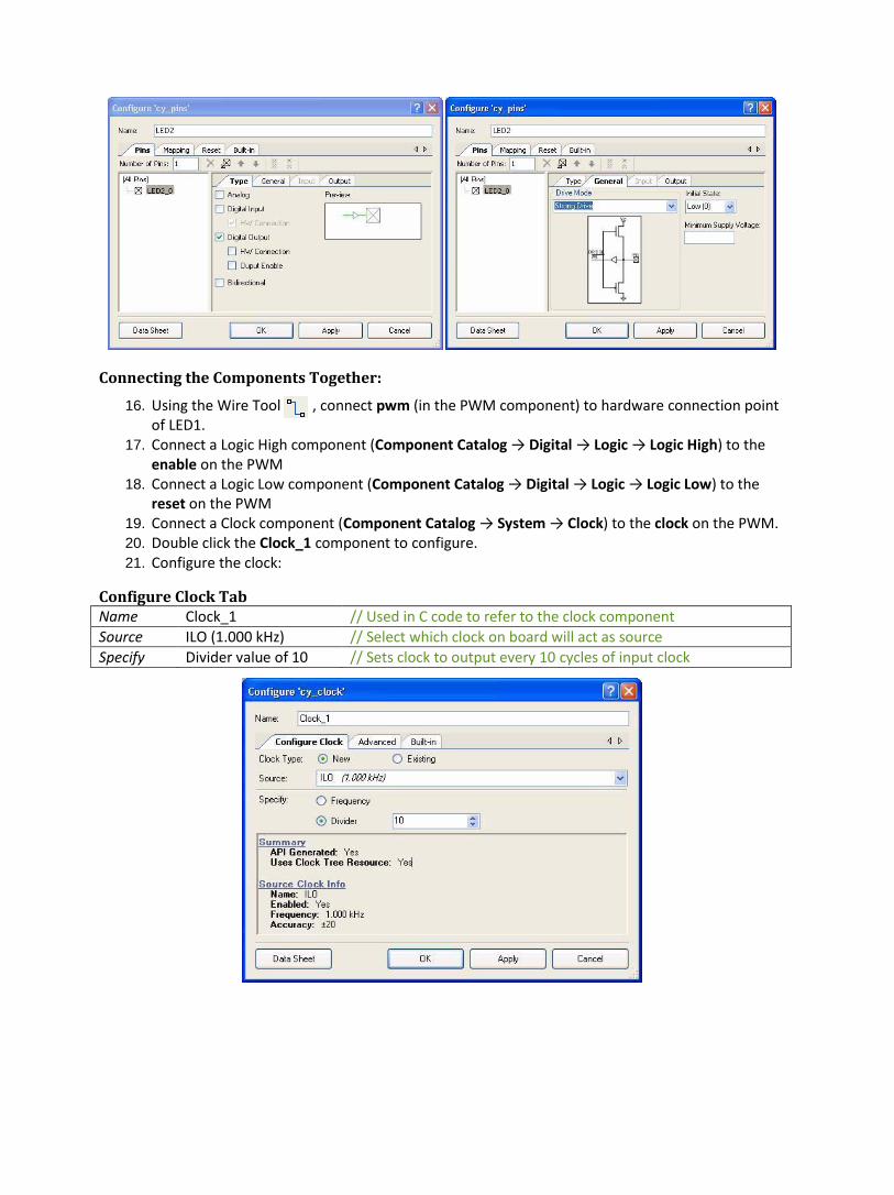
19. Connect a Clock component (Component Catalog → System → Clock) to the clock on the PWM. 20. Double click the Clock_1 component to configure. 21. Configure the clock:
Configure Clock Tab Name Clock_1 // Used in C code to refer to the clock component
Source ILO (1.000 kHz) // Select which clock on board will act as source
Specify Divider value of 10 // Sets clock to output every 10 cycles of input clock

22. When complete the schematic looks similar to:
Configuring the Pins:
23. From the Workspace Explorer, double click the Ex1_LED_with_PWM.cydwr file 24. Click the Pins tab. 25. Select pin P1[6] for LED1. 26. Select pin P1[7] for LED2.
Creating the main.c File: 27. Open the existing main.c file within Workspace Explorer. 28. Replace the existing main.c content with the content of the embedded PA1-LED.c file, which can
be found at: http://www.cse.ucsd.edu/~kastner/cse30/PA1-LED.c 29. From the Build menu, select Build Ex1_LED_with_PWM. 30. PSoC Creator builds the project and displays the comments in the Output dialog box. When you
see the message "Build Succeeded" the build is complete.

Configuring the PSoC Development Board:
31. Set supply voltage by switching SW3 to 3.3V. It is located next to the power supply and 9v battery connector.
32. Configure the following on the PSoC Development Board's prototyping area using the included 33. jumper wires
a. P1[6] to LED1 b. P1[7] to LED2
34. Connect the power supply to the board
Programming the PSoC Development Board:
35. Connect MiniProg3 to J5 (the pins that read PROG) on the CY8C55 Family Processor Module (the board cannot be programmed directly via the USB port on board)
If this is your first time running PSoC Creator, follow these steps to configure the MiniProg3 device for these PSoC Development Kit projects. If these configurations are set, skip to the next step below and begin programming.
Note: VTARG of the MiniProg3 is wired exclusively to VDDIO1 of the chip on the PSoC CY8C55 Family Processor Module. Because of this, you cannot perform power cycle mode programming.
36. From the Tools menu in PSoC Creator, click Options. 37. In the Options window, select Program/Debug from the list.
a. Set Applied Voltage to 3.3V b. Set Transfer Mode to SWD c. Set Active Port to 10 Pin d. Set Debug Clock Speed to 3.2 MHz e. Click OK
38. From the Debug menu, select Select Debug Target. a. Expand the tree under MiniProg3 and click Port Acquire. b. Select the appropriate device and click Connect. c. Click OK.
39. In PSoC Creator, from the Debug menu, click Program.

40. The PSoC Creator Status Bar indicates that the device is programming. 41. Wait until programming is complete before continuing. 42. Connect P1[6] to LED1 and P1[7] to LED2. Verify that LED1 and LED2 are blinking based on the
project's use of the PWMs. 43. LED1 blinks approximately once every second and LED 2 blinks about three times a second.
Now that you have completed your first project, let’s move on to a small introduction to using the other useful components on this board. In the following guided exercise, you will be using the potentiometer (the small black dial to the left of the touch-sensing sliders) to control the brightness of the LCD display.
LED 1:
The PWM used in this project is configured to produce a digital signal with a period of 100 cycles of the source clock, and a 50% duty cycle. The source clock runs at 100Hz, resulting in a 1Hz square wave being output from the PWM to drive LED 1.
LED 2:
The main.c function uses an infinite loop and a delay function to periodically toggle the output for LED 2. By delaying by 167 milliseconds, this loop is producing a 3Hz square wave.

Example Project #2: ADC to LCD Project
Overview:
This project demonstrates the Delta Sigma ADC by measuring the voltage of the potentiometer on the board and displays the result on the Character LCD of the PSoC Development Board. The ADC is clocked by the internal clock of 3 MHz and the sampling rate is set to 10,000 sps. Connect the voltage potentiometer (labeled "VR" on the PSoC Development Board) to the ADC input (programmed to P0[7] for this example). The program reads the ADC result and prints it to the LCD.
Creating the Project:
1. Open PSoC Creator. 2. Create a new project by clicking Create New Project… in the Start Page of PSoC Creator. 3. In the New Project window, select Empty PSoC5 Design template for a PSoC 5 design and Name
the project Ex2_ADC_to_LCD. 4. In Location, type the path where you want to save the project, or click and navigate to the
appropriate directory. By default, the design window opens TopDesign.cysch. This is the project's schematic entry file within PSoC Creator.
Placing and Configuring Delta Sigma ADC:
5. Drag and drop the Delta Sigma ADC component (Component Catalog → Analog → ADC → Delta Sigma ADC)
6. Double click the ADC_DelSig_1 component in the schematic to open the configuration window. 7. Configure the Delta Sigma ADC in this manner:
Configure - Config 1 Tab Name ADC_DelSig_1 // Used in C code to refer to the ADC component
# Configs 1 // Allows developer to design multiple configurations
Conversion Mode Continuous // Set based on expected type of input
Resolution 8 // Number of bits to use for granularity of measurement
Conversion Rate 10000 // Samples per second to be taken
Input Mode Single // Compares input to ground rather than second input
Input Range Vssa to Vdda // Input ranges from ground to supply voltage
Buffer Gain 1 // Required gain value for input range
Configure – Common Tab Clock Source internal // ADC will use internal clk instead of external clk in TopDesign
Hardware SOC Unchecked //The start of conversion will be triggered by software
For more information about what the parameters mean, click the Data Sheet button in the config-uration window.
Delta Sigma Analog-to-Digital Converter (ADC)
The ADC used in this lab measures the voltage from the potentiometer and express it as an 8-bit unsigned integer value where a value of 0 (0x00) signifies a voltage of Vssa and 255 (0xFF) signifies a voltage of Vdda.
Delta Sigma modulation is the technique used to make these measurements. The input voltage is passed to an oscillator. The oscillator produces pulses with a period inversely proportional to the voltage (i.e. the higher the voltage the more frequent the pulses). The digital output is computed by counting the pulses.

Placing and Configuring an Analog Pin:
8. Drag-and-drop the analog pin component (Component Catalog → Ports and Pins → Analog Pin).
9. Double click on the Pin_1 component in the schematic to open the configuration window. 10. Configure the analog pin in this manner
Type Tab Name POT // Used in C code to refer to the POT input pin
Analog Selected // Define pin as an analog input
*Leave all other boxes unchecked
General Tab Drive Mode High Impedance Analog // Set hardware configuration for input pin
*Leave remaining parameters as default
Potentiometer (POT)
A Potentiometer is a variable resistor that works by having a conductive wiper sweep across a resistive material. Thus, the further the wiper is from either the A or B pins, the greater resistance there will be between that pin and the W pin.

Placing and Configuring Character LCD:
11. Drag-and-drop the Character LCD component (Component Catalog → Display → Character LCD) 12. Double click the LCD_Char_1 component in the schematic to open the configuration window. 13. Configure the Character LCD
General Tab LCD Custom Character Set None // Set to use software defined text
Include ASCII to Number Conversion routines Selected // Enables several API routines
For more information about what the parameters mean, click the Data Sheet button in the config-uration window.
Liquid Crystal Display (LCD)
While in recent years LCDs have become the primary display technology for TVs, they have existed since the late eighties. LCDs do not produce light, but rather rely on incident light or backlighting. The basic technology uses two linear polarizer plates that are perpendicular to each other. When incident light passes through the first plate, it becomes polarized to that plate’s orientation. When the light reaches the second plate it is blocked by the polarizer.
No Voltage Max Voltage
To allow light to pass through, liquid crystals are arranged in a helical structure between the two plates. This causes the polarized light to be rotated to the orientation of the second polarizer, allowing it to pass through. When voltage is applied to electrodes in contact with the liquid crystals, begin to untwist, thus reducing the amount of light allowed through the front polarizer. With enough voltage, the crystals will completely straighten, and the light will be blocked.

Connecting the Components Together:
14. Wire the POT analog port to the ADC_DelSig_1 input. 15. When complete, the schematic looks like the figure below.
Configuring the Pins:
16. From the Workspace Explorer, double click the Ex2_ADC_to_LCD.cydwr file. 17. Click the Pins tab. 18. Select pins P2[6:0] for LCD_Char_1. 19. Select pin P0[7] for POT
Creating the main.c File:
20. Open the existing main.c file within Workspace Explorer. 21. Replace the existing main.c content with the content of the PA1-VR.c file, which can be found at
http://cseweb.ucsd.edu/~kastner/cse30/PA1-VR.c 22. From the Build menu, select Build Ex2_ADC_to_LCD. PSoC Creator builds the project and dis-
plays the comments in the Output dialog box. When you see the message "Build Succeeded" the build is complete.
Configuring and Programming the PSoC Development Board:
23. Using the jumper wires included, configure the PSoC Development Board's prototyping. Connect P0[7] to the VR pin located directly below the breadboard.
24. Verify that VR_PWR (J11) is jumpered to ON. 25. Apply power to the board 26. Use PSoC Creator as described in the previous project to program the device. 27. After programming the device, press the Reset button on the PSoC Development Board to see
the output of the ADC displayed on the LCD. Turning the potentiometer results in the LCD value changing.

Finally, the Assignment:
Now that you have done these two examples, combine the two projects to toggle the rate of one LED blinking based upon the position of the potentiometer. This means that as you turn the potentiometer, the LED blinks at a faster/slower rate. Twisting the potentiometer clockwise makes the LED blink slower (this is when the ADC has a higher value), and twisting it counter clockwise increases the rate of the LED blinking (when the ADC has a lower value).
Check the forum for a video demonstration of what we expect.
Optional:
Have the potentiometer control the blink rate for two LEDs, one through software and the other using a PWM.
Questions:
Explain how you would modify your solution to the assignment, using only components covered in this lab, so that turning the potentiometer dims the LED rather than causing it to blink?
If our development board hadn’t included a potentiometer, how could you have made one using common household materials?