Embed Size (px)
Citation preview
CLB
CLB
CLB
CLB
SwitchMatrix
ProgrammableInterconnect
I/O Blocks (IOBs)
ConfigurableLogic Blocks (CLBs)
D Q
SlewRate
Control
PassivePull-Up,
Pull-Down
Delay
Vcc
OutputBuffer
InputBuffer
Q D
Pad
D QSD
RD
EC
S/RControl
D QSD
RD
EC
S/RControl
1
1
F'
G'
H'
DIN
F'
G'
H'
DIN
F'
G'
H'
H'
HFunc.Gen.
GFunc.Gen.
FFunc.Gen.
G4G3G2G1
F4F3F2F1
C4C1 C2 C3
K
Y
X
H1 DIN S/R EC
Applications of FPGAs
n Implementation of random logicn easier changes at system-level (one device is modified)n can eliminate need for full-custom chips
n Prototypingn ensemble of gate arrays used to emulate a circuit to be manufacturedn get more/better/faster debugging done than possible with simulation
n Reconfigurable hardwaren one hardware block used to implement more than one functionn functions must be mutually-exclusive in timen can greatly reduce cost while enhancing flexibilityn RAM-based only option
n Special-purpose computation enginesn hardware dedicated to solving one problem (or class of problems)n accelerators attached to general-purpose computers
trend toward higher levels of integration
Evolution of implementation technologies
n Logic gates (1950s-60s)
n Regular structures for two-level logic (1960s-70s)
n muxes and decoders, PLAs
n Programmable sum-of-products arrays (1970s-80s)
n PLDs, complex PLDs
n Programmable gate arrays (1980s-90s)
n densities high enough to permit entirely newclass of application, e.g., prototyping, emulation,acceleration
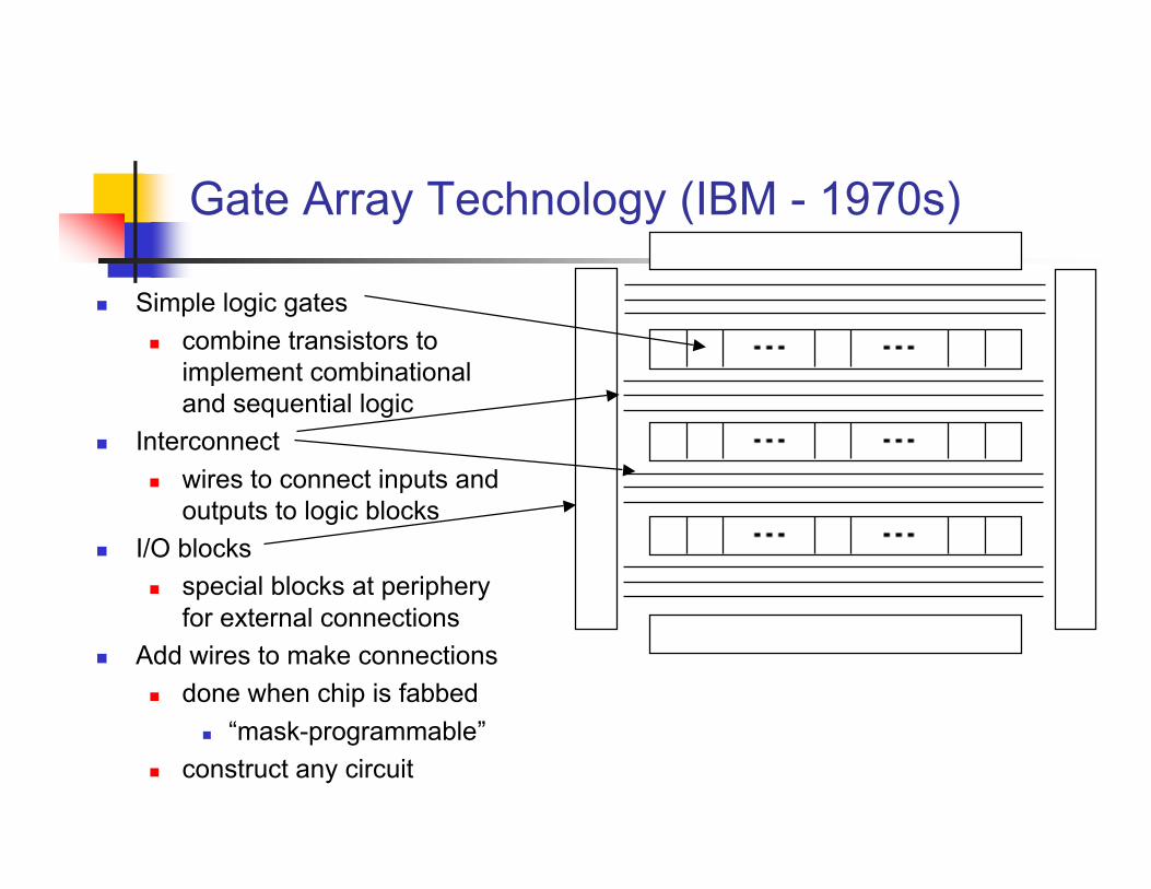
Gate Array Technology (IBM - 1970s)
n Simple logic gates
n combine transistors toimplement combinationaland sequential logic
n Interconnect
n wires to connect inputs andoutputs to logic blocks
n I/O blocks
n special blocks at peripheryfor external connections
n Add wires to make connections
n done when chip is fabbed
n “mask-programmable”
n construct any circuit
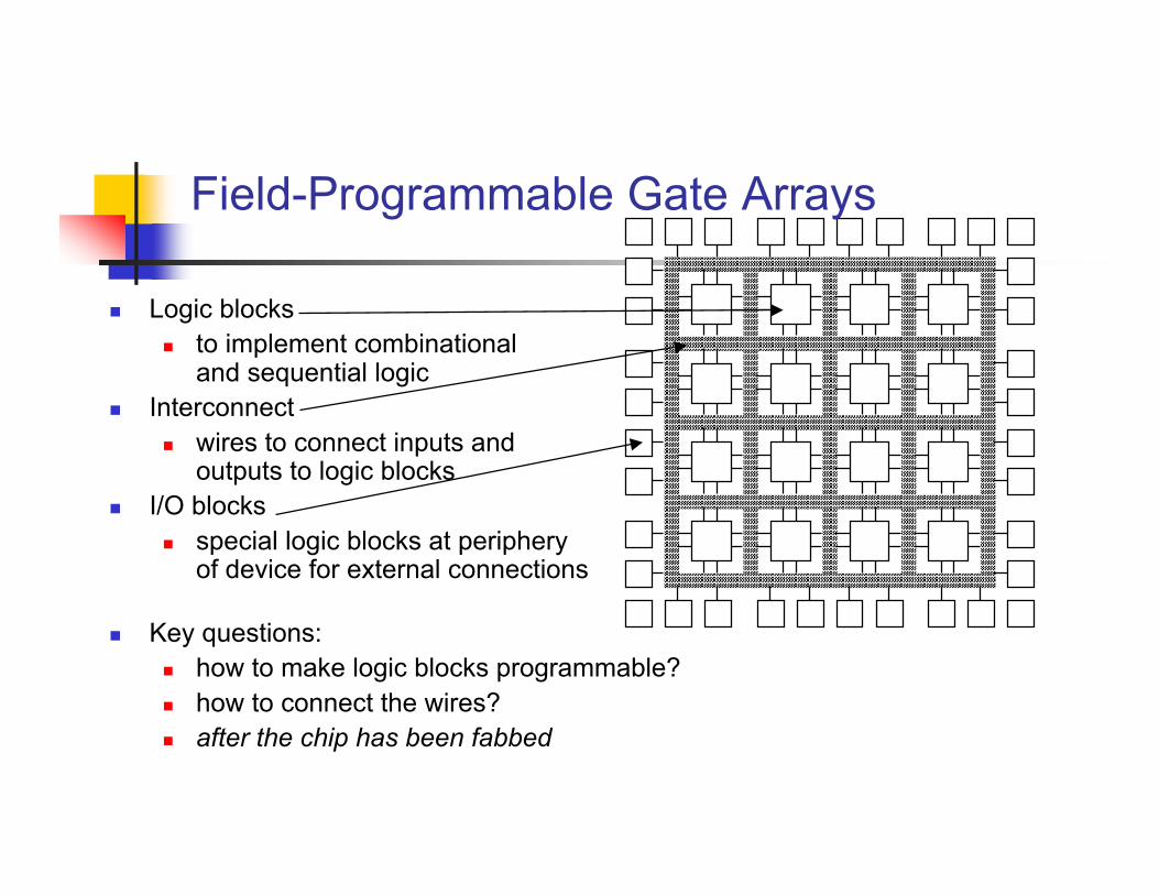
Field-Programmable Gate Arrays
n Logic blocksn to implement combinational
and sequential logicn Interconnect
n wires to connect inputs andoutputs to logic blocks
n I/O blocksn special logic blocks at periphery
of device for external connections
n Key questions:n how to make logic blocks programmable?n how to connect the wires?n after the chip has been fabbed
Enabling Technology
n Cheap/fast fuse connections
n small area (can fit lots of them)
n low resistance wires (fast even if in multiple segments)
n very high resistance when not connected
n small capacitance (wires can be longer)
n Pass transistors (switches)
n used to connect wires
n bi-directional
n Multiplexors
n used to connect one of a set of possible sources to input
n can be used to implement logic functions
Programming Technologies
n Fuse and anti-fuse
n fuse makes or breaks link between two wires
n typical connections are 50-300 ohm
n one-time programmable (testing before programming?)
n EPROM and EEPROM
n high power consumption
n typical connections are 2K-4K ohm
n fairly low density
n RAM-based
n memory bit controls a switch that connects/disconnects two wires
n typical connections are .5K-1K ohm
n can be programmed and re-programmed easily (tested at factory)
Tradeoffs in FPGAs
n Logic block - how are functions implemented: fixed functions(manipulate inputs) or programmable?n support complex functions, need fewer blocks, but they are bigger
so less of them on chipn support simple functions, need more blocks, but they are smaller so
more of them on chipn Interconnect
n how are logic blocks arranged?n how many wires will be needed between them?n are wires evenly distributed across chip?n programmability slows wires down – are some wires specialized to
long distances?n how many inputs/outputs must be routed to/from each logic block?n what utilization are we willing to accept? 50%? 20%? 90%?
IOB IOB IOB IOB
CLB CLB
CLB CLB
IOB
IOB
IOB
IOB
Wiring Channels
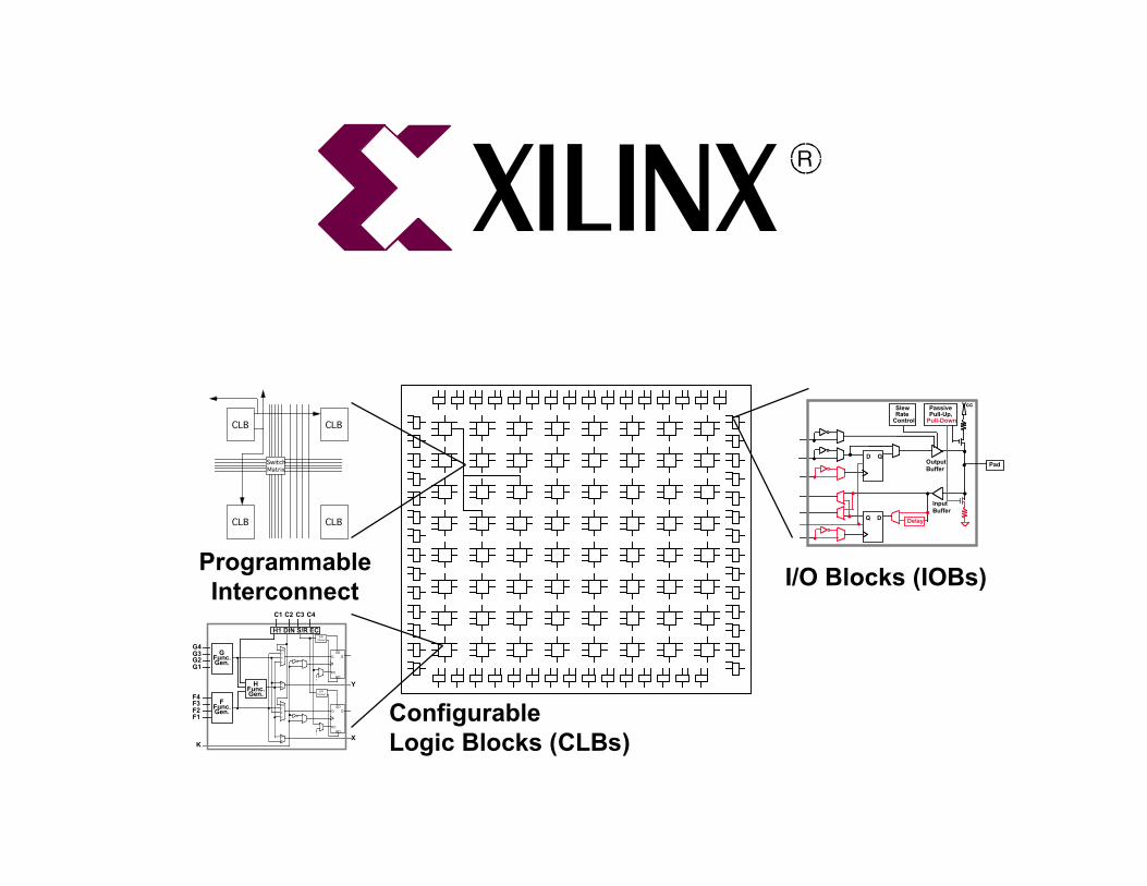
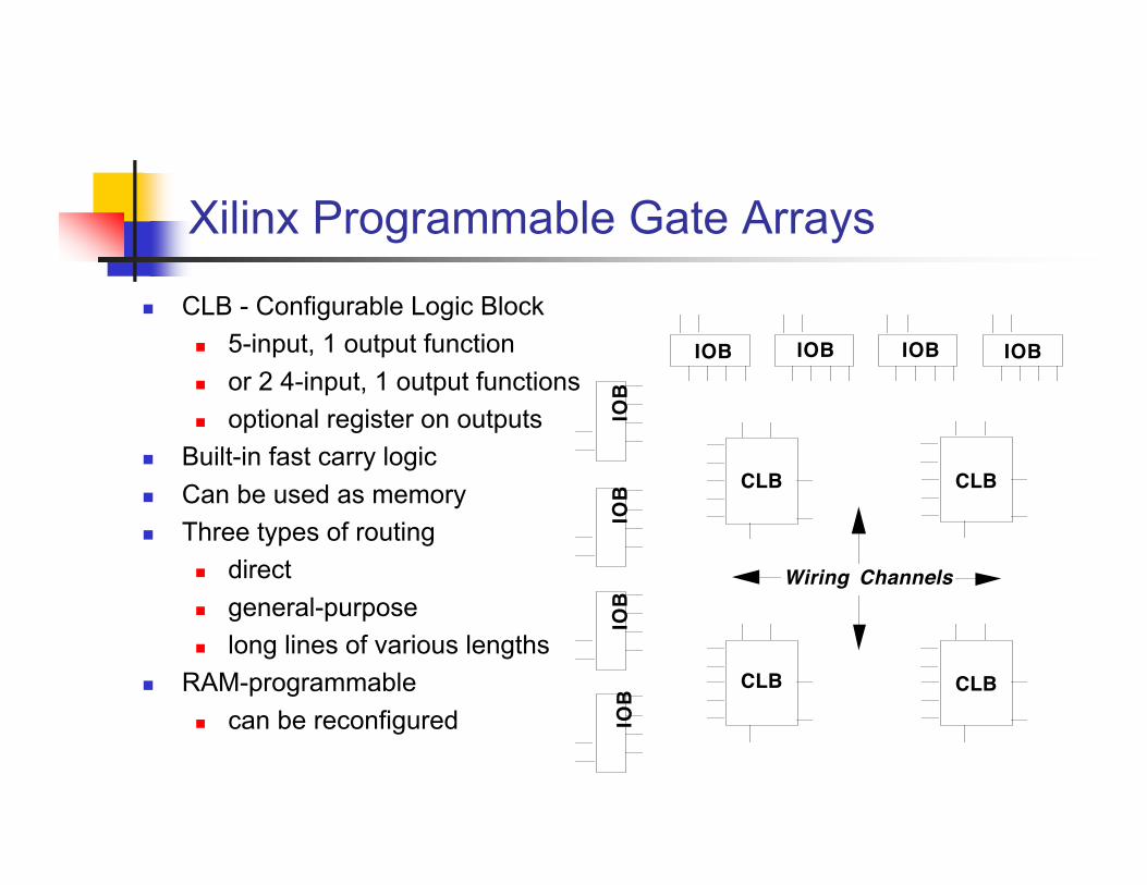
Xilinx Programmable Gate Arrays
n CLB - Configurable Logic Block
n 5-input, 1 output function
n or 2 4-input, 1 output functions
n optional register on outputs
n Built-in fast carry logic
n Can be used as memory
n Three types of routing
n direct
n general-purpose
n long lines of various lengths
n RAM-programmable
n can be reconfigured
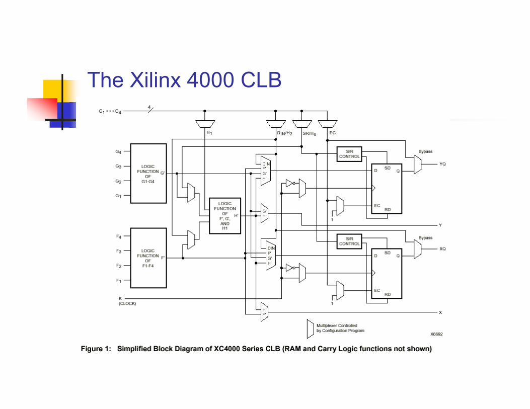
The Xilinx 4000 CLB
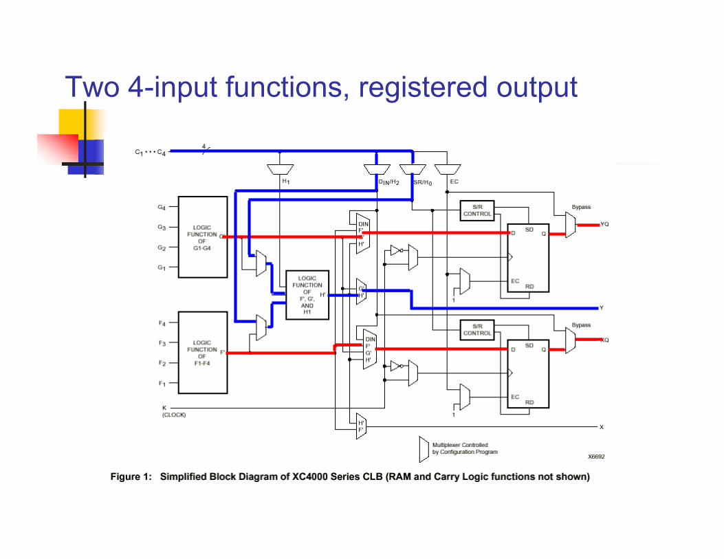
Two 4-input functions, registered output
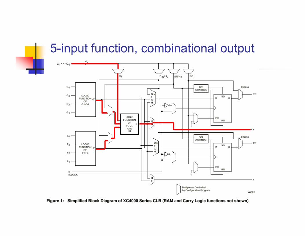
5-input function, combinational output
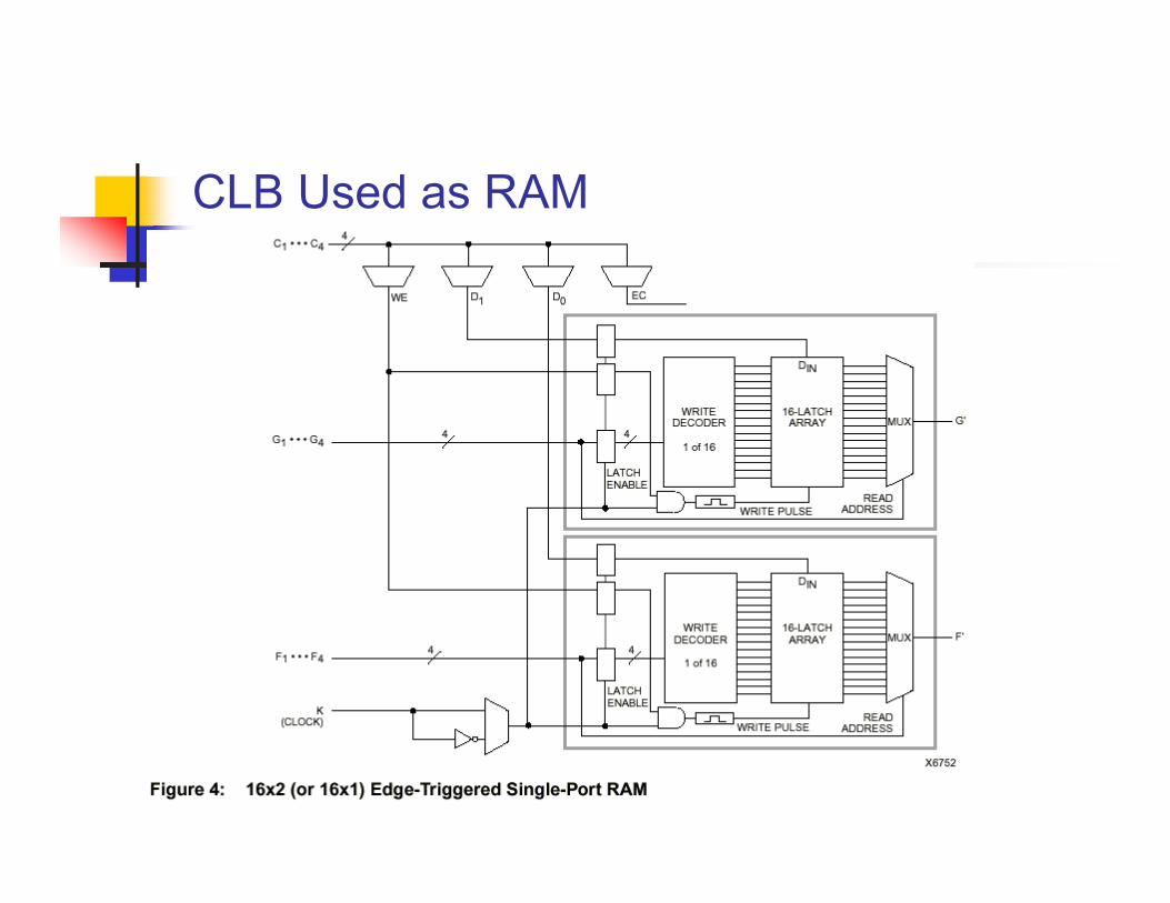
CLB Used as RAM
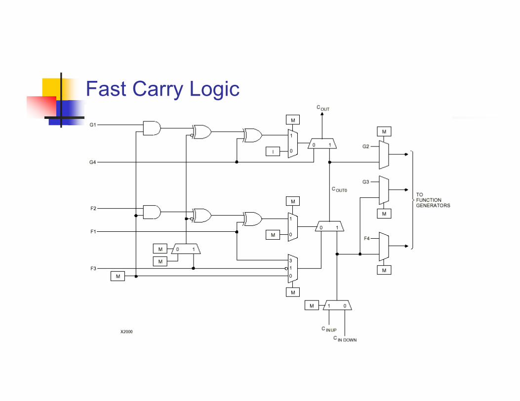
Fast Carry Logic
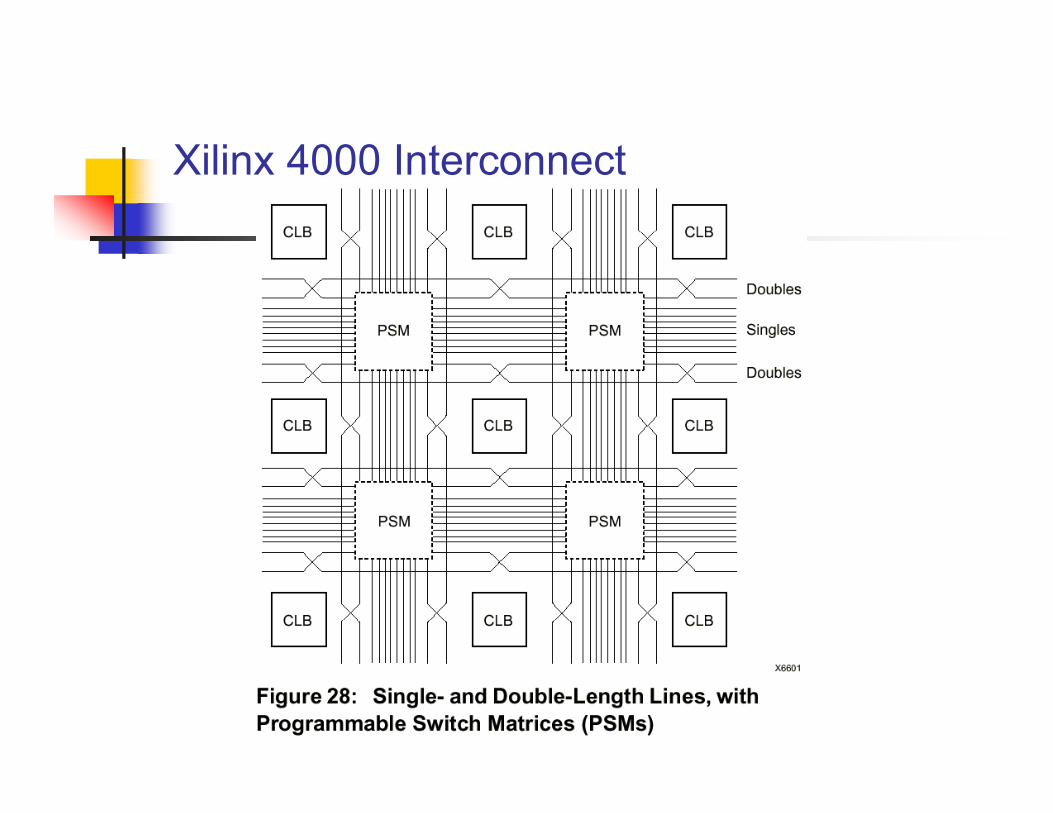
Xilinx 4000 Interconnect
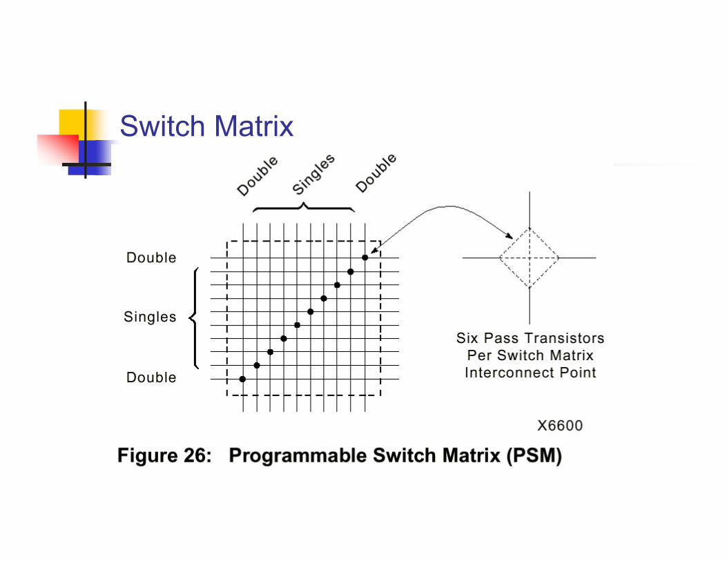
Switch Matrix
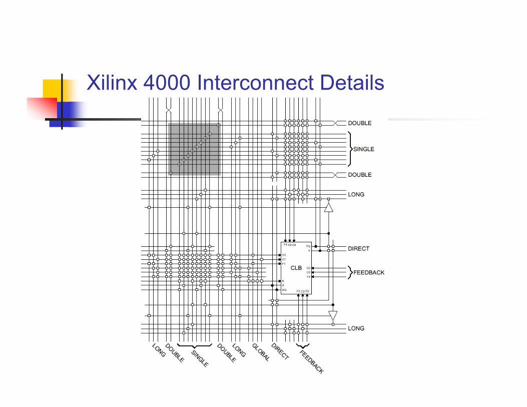
Xilinx 4000 Interconnect Details
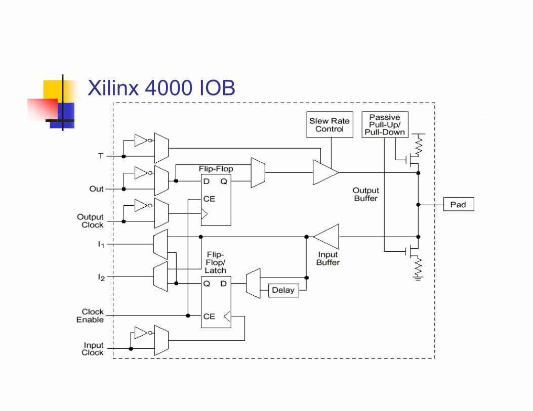
Xilinx 4000 IOB
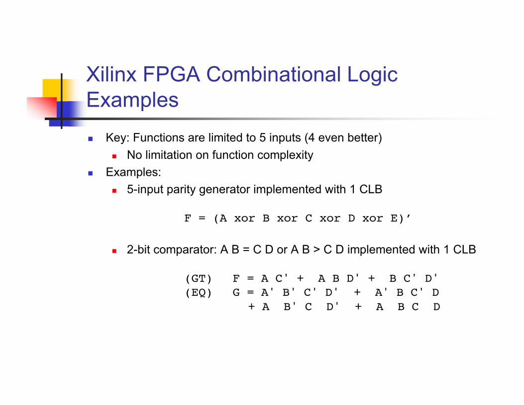
Xilinx FPGA Combinational LogicExamples
n Key: Functions are limited to 5 inputs (4 even better)
n No limitation on function complexity
n Examples:
n 5-input parity generator implemented with 1 CLB
F = (A xor B xor C xor D xor E)’
n 2-bit comparator: A B = C D or A B > C D implemented with 1 CLB
(GT) F = A C' + A B D' + B C' D'(EQ) G = A' B' C' D' + A' B C' D
+ A B' C D' + A B C D
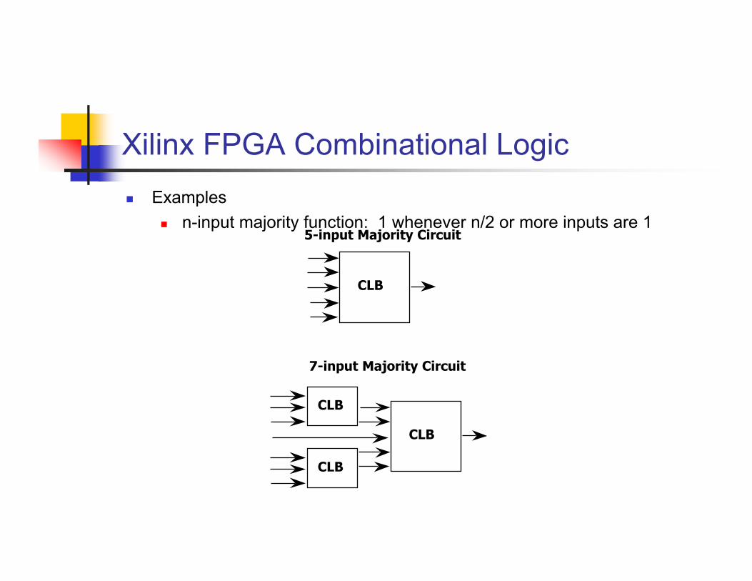
CLB
5-input Majority Circuit
CLB
CLB
CLB
7-input Majority Circuit
Xilinx FPGA Combinational Logic
n Examples
n n-input majority function: 1 whenever n/2 or more inputs are 1
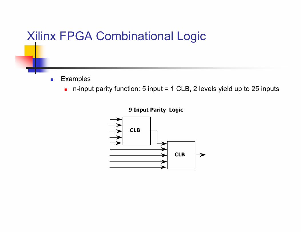
CLB
CLB
9 Input Parity Logic
Xilinx FPGA Combinational Logic
n Examples
n n-input parity function: 5 input = 1 CLB, 2 levels yield up to 25 inputs
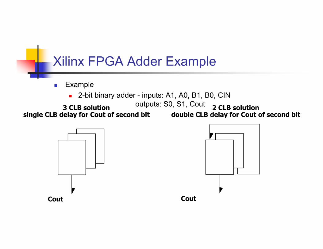
CoutCout
3 CLB solutionsingle CLB delay for Cout of second bit
2 CLB solutiondouble CLB delay for Cout of second bit
Xilinx FPGA Adder Example
n Example
n 2-bit binary adder - inputs: A1, A0, B1, B0, CIN outputs: S0, S1, Cout
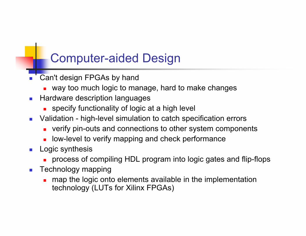
Computer-aided Design
n Can't design FPGAs by handn way too much logic to manage, hard to make changes
n Hardware description languagesn specify functionality of logic at a high level
n Validation - high-level simulation to catch specification errorsn verify pin-outs and connections to other system componentsn low-level to verify mapping and check performance
n Logic synthesisn process of compiling HDL program into logic gates and flip-flops
n Technology mappingn map the logic onto elements available in the implementation
technology (LUTs for Xilinx FPGAs)
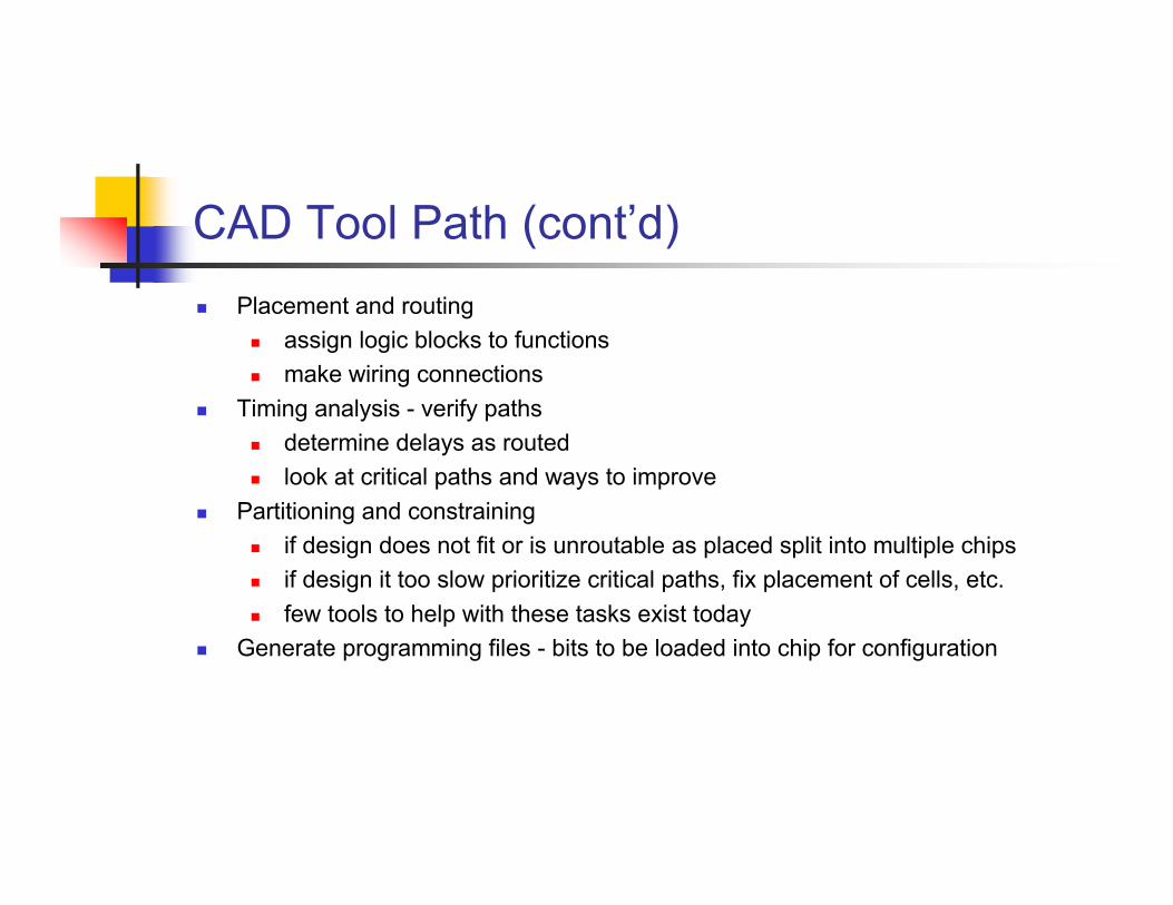
CAD Tool Path (cont’d)
n Placement and routing
n assign logic blocks to functions
n make wiring connections
n Timing analysis - verify paths
n determine delays as routed
n look at critical paths and ways to improve
n Partitioning and constraining
n if design does not fit or is unroutable as placed split into multiple chips
n if design it too slow prioritize critical paths, fix placement of cells, etc.
n few tools to help with these tasks exist today
n Generate programming files - bits to be loaded into chip for configuration


![L16: Power Dissipation in Digital Systemsweb.mit.edu/6.111/www/s2006/LECTURES/l16.pdf · [Montanaro, JSSC ‘96] [A. Sinha, DAC] 65% 21% 9% 5% Interconnect Clock I/O CLB CLB CLB CLB](https://img.pdfslide.us/doc/110x75/6075f07be9a488213651b8cd/l16-power-dissipation-in-digital-montanaro-jssc-a96-a-sinha-dac-65-21.jpg)