Embed Size (px)
Citation preview
®
APEX 20KCProgrammable Logic
Device
February 2004 ver. 2.2 Data Sheet
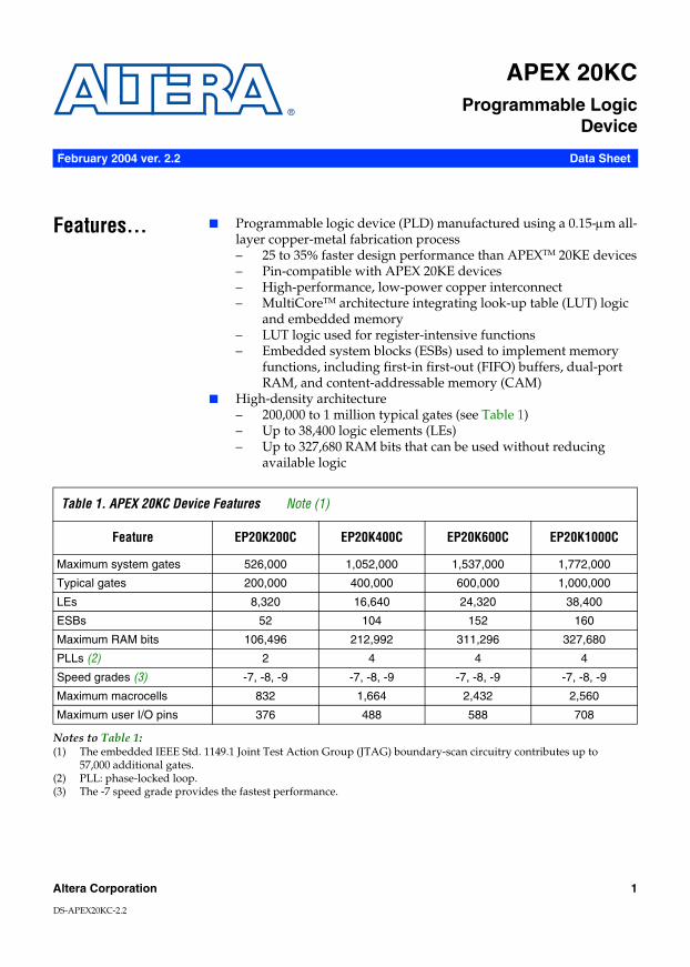
Features... Programmable logic device (PLD) manufactured using a 0.15-µm all-layer copper-metal fabrication process– 25 to 35% faster design performance than APEXTM 20KE devices– Pin-compatible with APEX 20KE devices– High-performance, low-power copper interconnect– MultiCoreTM architecture integrating look-up table (LUT) logic
and embedded memory– LUT logic used for register-intensive functions– Embedded system blocks (ESBs) used to implement memory
functions, including first-in first-out (FIFO) buffers, dual-port RAM, and content-addressable memory (CAM)
High-density architecture– 200,000 to 1 million typical gates (see Table 1)– Up to 38,400 logic elements (LEs)– Up to 327,680 RAM bits that can be used without reducing
available logic
Notes to Table 1:(1) The embedded IEEE Std. 1149.1 Joint Test Action Group (JTAG) boundary-scan circuitry contributes up to
57,000 additional gates.(2) PLL: phase-locked loop.(3) The -7 speed grade provides the fastest performance.
Table 1. APEX 20KC Device Features Note (1)
Feature EP20K200C EP20K400C EP20K600C EP20K1000C
Maximum system gates 526,000 1,052,000 1,537,000 1,772,000
Typical gates 200,000 400,000 600,000 1,000,000
LEs 8,320 16,640 24,320 38,400
ESBs 52 104 152 160
Maximum RAM bits 106,496 212,992 311,296 327,680
PLLs (2) 2 4 4 4
Speed grades (3) -7, -8, -9 -7, -8, -9 -7, -8, -9 -7, -8, -9
Maximum macrocells 832 1,664 2,432 2,560
Maximum user I/O pins 376 488 588 708
Altera Corporation 1
DS-APEX20KC-2.2
APEX 20KC Programmable Logic Device Data Sheet
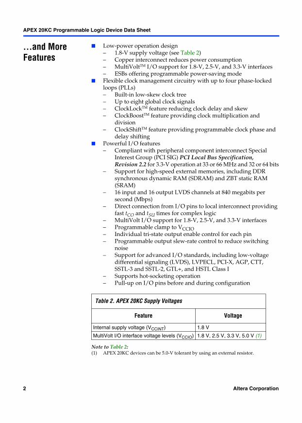
...and More Features
Low-power operation design– 1.8-V supply voltage (see Table 2)– Copper interconnect reduces power consumption– MultiVoltTM I/O support for 1.8-V, 2.5-V, and 3.3-V interfaces– ESBs offering programmable power-saving mode
Flexible clock management circuitry with up to four phase-locked loops (PLLs)– Built-in low-skew clock tree– Up to eight global clock signals– ClockLockTM feature reducing clock delay and skew– ClockBoostTM feature providing clock multiplication and
division– ClockShiftTM feature providing programmable clock phase and
delay shifting Powerful I/O features
– Compliant with peripheral component interconnect Special Interest Group (PCI SIG) PCI Local Bus Specification, Revision 2.2 for 3.3-V operation at 33 or 66 MHz and 32 or 64 bits
– Support for high-speed external memories, including DDR synchronous dynamic RAM (SDRAM) and ZBT static RAM (SRAM)
– 16 input and 16 output LVDS channels at 840 megabits per second (Mbps)
– Direct connection from I/O pins to local interconnect providing fast tCO and tSU times for complex logic
– MultiVolt I/O support for 1.8-V, 2.5-V, and 3.3-V interfaces– Programmable clamp to VCCIO– Individual tri-state output enable control for each pin– Programmable output slew-rate control to reduce switching
noise– Support for advanced I/O standards, including low-voltage
differential signaling (LVDS), LVPECL, PCI-X, AGP, CTT, SSTL-3 and SSTL-2, GTL+, and HSTL Class I
– Supports hot-socketing operation– Pull-up on I/O pins before and during configuration
Note to Table 2:(1) APEX 20KC devices can be 5.0-V tolerant by using an external resistor.
Table 2. APEX 20KC Supply Voltages
Feature Voltage
Internal supply voltage (VCCINT) 1.8 V
MultiVolt I/O interface voltage levels (VCCIO) 1.8 V, 2.5 V, 3.3 V, 5.0 V (1)
2 Altera Corporation
APEX 20KC Programmable Logic Device Data Sheet
Advanced interconnect structure– Copper interconnect for high performance– Four-level hierarchical FastTrack® interconnect structure
providing fast, predictable interconnect delays– Dedicated carry chain that implements arithmetic functions such
as fast adders, counters, and comparators (automatically used by software tools and megafunctions)
– Dedicated cascade chain that implements high-speed, high-fan-in logic functions (automatically used by software tools and megafunctions)
– Interleaved local interconnect allows one LE to drive 29 other LEs through the fast local interconnect
Advanced software support– Software design support and automatic place-and-route
provided by the Altera® QuartusTM II development system for Windows-based PCs, Sun SPARCstations, and HP 9000 Series 700/800 workstations
– Altera MegaCore® functions and Altera Megafunction Partners Program (AMPPSM) megafunctions optimized for APEX 20KC architecture available
– NativeLinkTM integration with popular synthesis, simulation, and timing analysis tools
– Quartus II SignalTap® embedded logic analyzer simplifies in-system design evaluation by giving access to internal nodes during device operation
– Supports popular revision-control software packages including PVCS, RCS, and SCCS
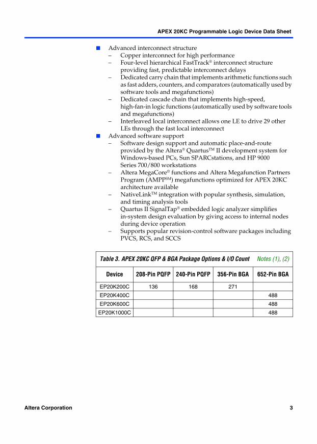
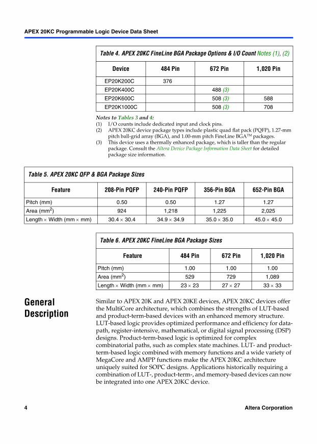
Table 3. APEX 20KC QFP & BGA Package Options & I/O Count Notes (1), (2)
Device 208-Pin PQFP 240-Pin PQFP 356-Pin BGA 652-Pin BGA
EP20K200C 136 168 271
EP20K400C 488
EP20K600C 488
EP20K1000C 488
Altera Corporation 3
APEX 20KC Programmable Logic Device Data Sheet
Notes to Tables 3 and 4:(1) I/O counts include dedicated input and clock pins.(2) APEX 20KC device package types include plastic quad flat pack (PQFP), 1.27-mm
pitch ball-grid array (BGA), and 1.00-mm pitch FineLine BGATM packages.(3) This device uses a thermally enhanced package, which is taller than the regular
package. Consult the Altera Device Package Information Data Sheet for detailed package size information.
General Description
Similar to APEX 20K and APEX 20KE devices, APEX 20KC devices offer the MultiCore architecture, which combines the strengths of LUT-based and product-term-based devices with an enhanced memory structure. LUT-based logic provides optimized performance and efficiency for data-path, register-intensive, mathematical, or digital signal processing (DSP) designs. Product-term-based logic is optimized for complex combinatorial paths, such as complex state machines. LUT- and product-term-based logic combined with memory functions and a wide variety of MegaCore and AMPP functions make the APEX 20KC architecture uniquely suited for SOPC designs. Applications historically requiring a combination of LUT-, product-term-, and memory-based devices can now be integrated into one APEX 20KC device.
Table 4. APEX 20KC FineLine BGA Package Options & I/O Count Notes (1), (2)
Device 484 Pin 672 Pin 1,020 Pin
EP20K200C 376
EP20K400C 488 (3)
EP20K600C 508 (3) 588
EP20K1000C 508 (3) 708
Table 5. APEX 20KC QFP & BGA Package Sizes
Feature 208-Pin PQFP 240-Pin PQFP 356-Pin BGA 652-Pin BGA
Pitch (mm) 0.50 0.50 1.27 1.27
Area (mm2) 924 1,218 1,225 2,025
Length × Width (mm × mm) 30.4 × 30.4 34.9 × 34.9 35.0 × 35.0 45.0 × 45.0
Table 6. APEX 20KC FineLine BGA Package Sizes
Feature 484 Pin 672 Pin 1,020 Pin
Pitch (mm) 1.00 1.00 1.00
Area (mm2) 529 729 1,089
Length × Width (mm × mm) 23 × 23 27 × 27 33 × 33
4 Altera Corporation
APEX 20KC Programmable Logic Device Data Sheet
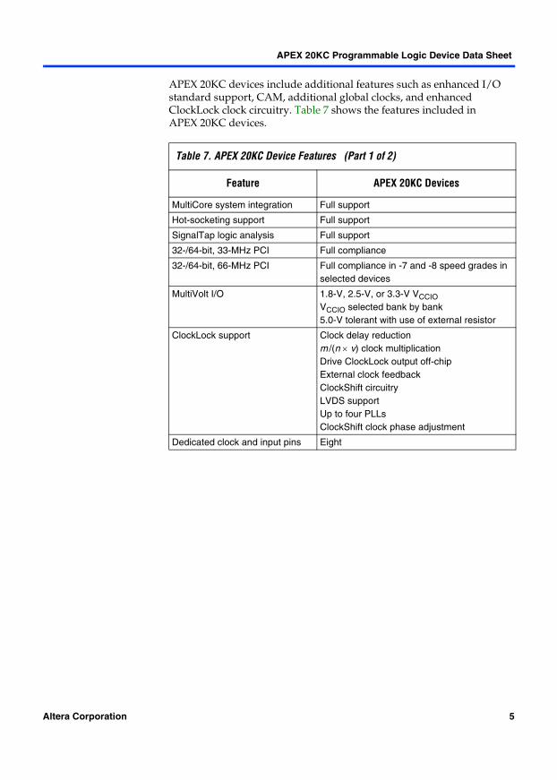
APEX 20KC devices include additional features such as enhanced I/O standard support, CAM, additional global clocks, and enhanced ClockLock clock circuitry. Table 7 shows the features included in APEX 20KC devices.
Table 7. APEX 20KC Device Features (Part 1 of 2)
Feature APEX 20KC Devices
MultiCore system integration Full support
Hot-socketing support Full support
SignalTap logic analysis Full support
32-/64-bit, 33-MHz PCI Full compliance
32-/64-bit, 66-MHz PCI Full compliance in -7 and -8 speed grades in selected devices
MultiVolt I/O 1.8-V, 2.5-V, or 3.3-V VCCIOVCCIO selected bank by bank5.0-V tolerant with use of external resistor
ClockLock support Clock delay reductionm /(n × v) clock multiplication Drive ClockLock output off-chipExternal clock feedbackClockShift circuitryLVDS supportUp to four PLLsClockShift clock phase adjustment
Dedicated clock and input pins Eight
Altera Corporation 5
APEX 20KC Programmable Logic Device Data Sheet
All APEX 20KC devices are reconfigurable and are 100% tested prior to shipment. As a result, test vectors do not have to be generated for fault-coverage purposes. Instead, the designer can focus on simulation and design verification. In addition, the designer does not need to manage inventories of different application-specific integrated circuit (ASIC) designs; APEX 20KC devices can be configured on the board for the specific functionality required.
APEX 20KC devices are configured at system power-up with data stored in an Altera serial configuration device or provided by a system controller. Altera offers in-system programmability (ISP)-capable EPC16, EPC8, EPC4, EPC2, and EPC1 configuration devices and one-time programmable (OTP) EPC1 configuration devices, which configure APEX 20KC devices via a serial data stream. Moreover, APEX 20KC devices contain an optimized interface that permits microprocessors to configure APEX 20KC devices serially or in parallel, and synchronously or asynchronously. The interface also enables microprocessors to treat APEX 20KC devices as memory and configure the device by writing to a virtual memory location, making reconfiguration easy.
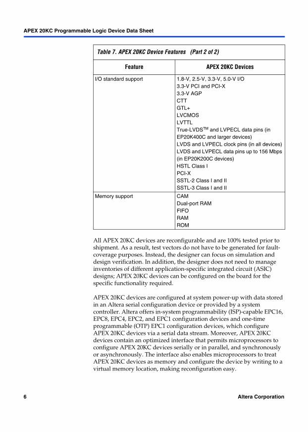
I/O standard support 1.8-V, 2.5-V, 3.3-V, 5.0-V I/O3.3-V PCI and PCI-X3.3-V AGPCTTGTL+LVCMOSLVTTLTrue-LVDSTM and LVPECL data pins (in EP20K400C and larger devices)LVDS and LVPECL clock pins (in all devices)LVDS and LVPECL data pins up to 156 Mbps (in EP20K200C devices)HSTL Class IPCI-XSSTL-2 Class I and IISSTL-3 Class I and II
Memory support CAMDual-port RAMFIFORAMROM
Table 7. APEX 20KC Device Features (Part 2 of 2)
Feature APEX 20KC Devices
6 Altera Corporation
APEX 20KC Programmable Logic Device Data Sheet
After an APEX 20KC device has been configured, it can be reconfigured in-circuit by resetting the device and loading new data. Real-time changes can be made during system operation, enabling innovative reconfigurable computing applications.
APEX 20KC devices are supported by the Altera Quartus II development system, a single, integrated package that offers HDL and schematic design entry, compilation and logic synthesis, full simulation and worst-case timing analysis, SignalTap logic analysis, and device configuration. The Quartus II software runs on Windows-based PCs, Sun SPARCstations, and HP 9000 Series 700/800 workstations.
The Quartus II software provides NativeLink interfaces to other industry-standard PC- and UNIX workstation-based EDA tools. For example, designers can invoke the Quartus II software from within third-party design tools. Further, the Quartus II software contains built-in optimized synthesis libraries; synthesis tools can use these libraries to optimize designs for APEX 20KC devices. For example, the Synopsys Design Compiler library, supplied with the Quartus II development system, includes DesignWare functions optimized for the APEX 20KC architecture.
Functional Description
APEX 20KC devices incorporate LUT-based logic, product-term-based logic, and memory into one device on an all-copper technology process. Signal interconnections within APEX 20KC devices (as well as to and from device pins) are provided by the FastTrack interconnect—a series of fast, continuous row and column channels that run the entire length and width of the device.
Each I/O pin is fed by an I/O element (IOE) located at the end of each row and column of the FastTrack interconnect. Each IOE contains a bidirectional I/O buffer and a register that can be used as either an input or output register to feed input, output, or bidirectional signals. When used with a dedicated clock pin, these registers provide exceptional performance. IOEs provide a variety of features, such as 3.3-V, 64-bit, 66-MHz PCI compliance; JTAG BST support; slew-rate control; and tri-state buffers. APEX 20KC devices offer enhanced I/O support, including support for 1.8-V I/O, 2.5-V I/O, LVCMOS, LVTTL, LVPECL, 3.3-V PCI, PCI-X, LVDS, GTL+, SSTL-2, SSTL-3, HSTL, CTT, and 3.3-V AGP I/O standards.
Altera Corporation 7
APEX 20KC Programmable Logic Device Data Sheet
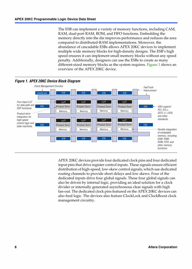
The ESB can implement a variety of memory functions, including CAM, RAM, dual-port RAM, ROM, and FIFO functions. Embedding the memory directly into the die improves performance and reduces die area compared to distributed-RAM implementations. Moreover, the abundance of cascadable ESBs allows APEX 20KC devices to implement multiple wide memory blocks for high-density designs. The ESB’s high speed ensures it can implement small memory blocks without any speed penalty. Additionally, designers can use the ESBs to create as many different-sized memory blocks as the system requires. Figure 1 shows an overview of the APEX 20KC device.
Figure 1. APEX 20KC Device Block Diagram
APEX 20KC devices provide four dedicated clock pins and four dedicated input pins that drive register control inputs. These signals ensure efficient distribution of high-speed, low-skew control signals, which use dedicated routing channels to provide short delays and low skews. Four of the dedicated inputs drive four global signals. These four global signals can also be driven by internal logic, providing an ideal solution for a clock divider or internally generated asynchronous clear signals with high fan-out. The dedicated clock pins featured on the APEX 20KC devices can also feed logic. The devices also feature ClockLock and ClockBoost clock management circuitry.
LUT
LUT
LUTLUT
LUT
Memory
Memory
Memory
Memory
IOE
IOE
IOE IOE
IOE
IOE
IOE IOE
LUT
LUT
Memory
Memory
IOE
IOE
Product Term
Product Term
LUT
LUT
Memory
Memory
IOE
IOE
Product Term
Product Term Product Term
Product Term Product Term
Product Term
FastTrack Interconnect
Clock Management Circuitry
IOEs support PCI, GTL+, SSTL-3, LVDS, and other standards.
ClockLock
Four-input LUT for data path and DSP functions.
Product-termintegration for high-speed control logic and state machines.
Flexible integration of embedded memory, including CAM, RAM, ROM, FIFO, and other memoryfunctions.
8 Altera Corporation
APEX 20KC Programmable Logic Device Data Sheet
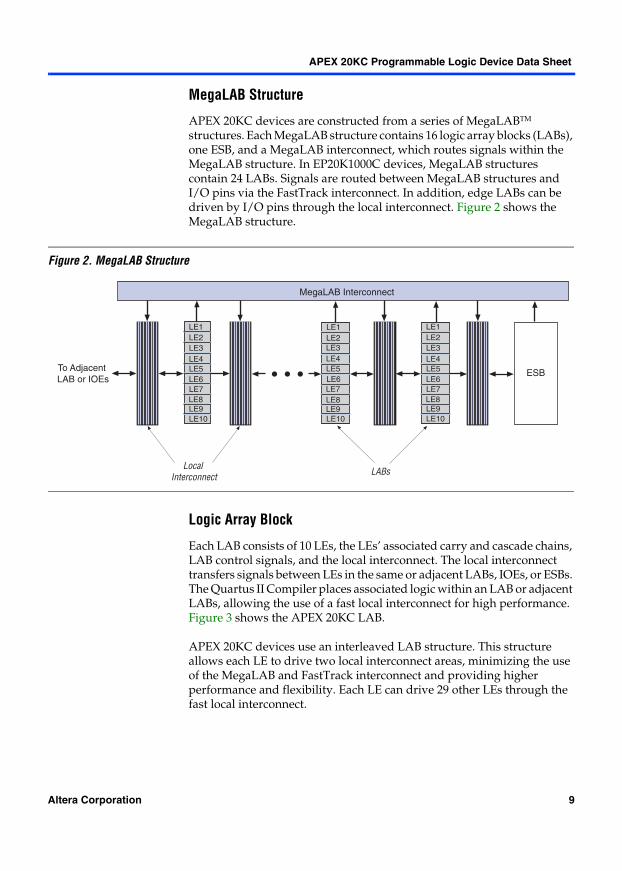
MegaLAB Structure
APEX 20KC devices are constructed from a series of MegaLABTM structures. Each MegaLAB structure contains 16 logic array blocks (LABs), one ESB, and a MegaLAB interconnect, which routes signals within the MegaLAB structure. In EP20K1000C devices, MegaLAB structures contain 24 LABs. Signals are routed between MegaLAB structures and I/O pins via the FastTrack interconnect. In addition, edge LABs can be driven by I/O pins through the local interconnect. Figure 2 shows the MegaLAB structure.
Figure 2. MegaLAB Structure
Logic Array Block
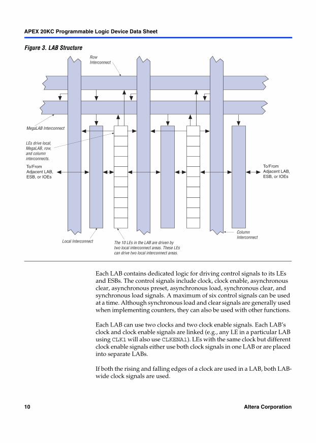
Each LAB consists of 10 LEs, the LEs’ associated carry and cascade chains, LAB control signals, and the local interconnect. The local interconnect transfers signals between LEs in the same or adjacent LABs, IOEs, or ESBs. The Quartus II Compiler places associated logic within an LAB or adjacent LABs, allowing the use of a fast local interconnect for high performance. Figure 3 shows the APEX 20KC LAB.
APEX 20KC devices use an interleaved LAB structure. This structure allows each LE to drive two local interconnect areas, minimizing the use of the MegaLAB and FastTrack interconnect and providing higher performance and flexibility. Each LE can drive 29 other LEs through the fast local interconnect.
ESB
MegaLAB Interconnect
Local Interconnect
To Adjacent LAB or IOEs
LABs
LE1LE2LE3LE4LE5LE6LE7LE8LE9LE10
LE1LE2LE3LE4LE5LE6LE7LE8LE9LE10
LE1LE2LE3LE4LE5LE6LE7LE8LE9LE10
Altera Corporation 9
APEX 20KC Programmable Logic Device Data Sheet
Figure 3. LAB Structure
Each LAB contains dedicated logic for driving control signals to its LEs and ESBs. The control signals include clock, clock enable, asynchronous clear, asynchronous preset, asynchronous load, synchronous clear, and synchronous load signals. A maximum of six control signals can be used at a time. Although synchronous load and clear signals are generally used when implementing counters, they can also be used with other functions.
Each LAB can use two clocks and two clock enable signals. Each LAB’s clock and clock enable signals are linked (e.g., any LE in a particular LAB using CLK1 will also use CLKENA1). LEs with the same clock but different clock enable signals either use both clock signals in one LAB or are placed into separate LABs.
If both the rising and falling edges of a clock are used in a LAB, both LAB-wide clock signals are used.
To/From Adjacent LAB,ESB, or IOEs
To/From Adjacent LAB,ESB, or IOEs
The 10 LEs in the LAB are driven by two local interconnect areas. These LEs can drive two local interconnect areas.
Local Interconnect
LEs drive local,MegaLAB, row, and column interconnects.
Column Interconnect
Row Interconnect
MegaLAB Interconnect
10 Altera Corporation
APEX 20KC Programmable Logic Device Data Sheet
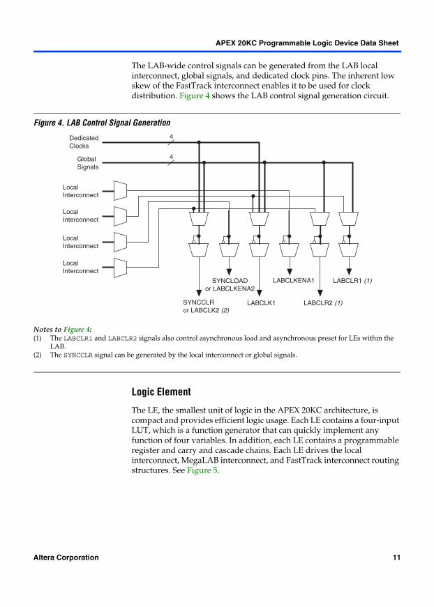
The LAB-wide control signals can be generated from the LAB local interconnect, global signals, and dedicated clock pins. The inherent low skew of the FastTrack interconnect enables it to be used for clock distribution. Figure 4 shows the LAB control signal generation circuit.
Figure 4. LAB Control Signal Generation
Notes to Figure 4:(1) The LABCLR1 and LABCLR2 signals also control asynchronous load and asynchronous preset for LEs within the
LAB.(2) The SYNCCLR signal can be generated by the local interconnect or global signals.
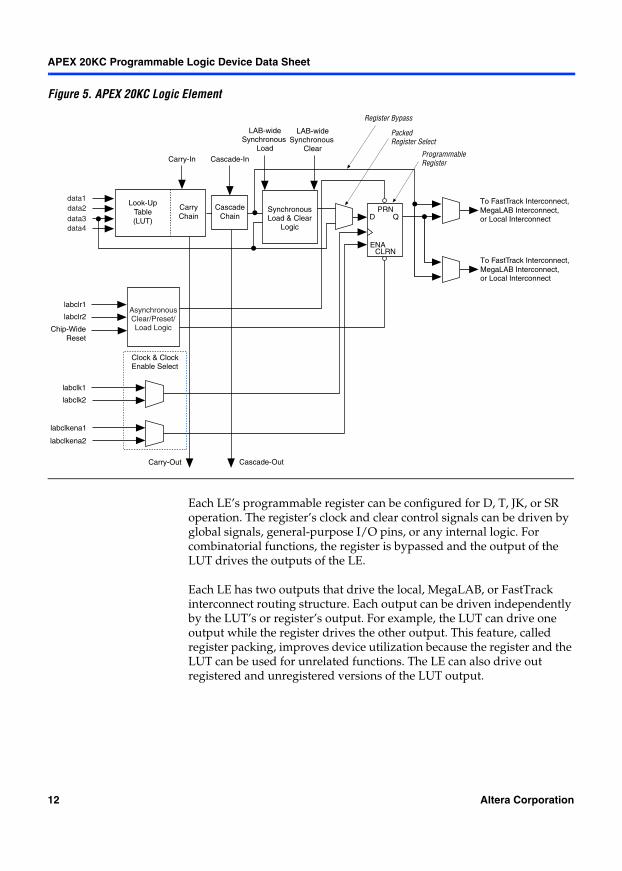
Logic Element
The LE, the smallest unit of logic in the APEX 20KC architecture, is compact and provides efficient logic usage. Each LE contains a four-input LUT, which is a function generator that can quickly implement any function of four variables. In addition, each LE contains a programmable register and carry and cascade chains. Each LE drives the local interconnect, MegaLAB interconnect, and FastTrack interconnect routing structures. See Figure 5.
SYNCCLRor LABCLK2 (2)
SYNCLOADor LABCLKENA2
LABCLK1
LABCLKENA1
LABCLR2 (1)
LABCLR1 (1)
DedicatedClocks
GlobalSignals
LocalInterconnect
LocalInterconnect
LocalInterconnect
LocalInterconnect
4
4
Altera Corporation 11
APEX 20KC Programmable Logic Device Data Sheet
Figure 5. APEX 20KC Logic Element
Each LE’s programmable register can be configured for D, T, JK, or SR operation. The register’s clock and clear control signals can be driven by global signals, general-purpose I/O pins, or any internal logic. For combinatorial functions, the register is bypassed and the output of the LUT drives the outputs of the LE.
Each LE has two outputs that drive the local, MegaLAB, or FastTrack interconnect routing structure. Each output can be driven independently by the LUT’s or register’s output. For example, the LUT can drive one output while the register drives the other output. This feature, called register packing, improves device utilization because the register and the LUT can be used for unrelated functions. The LE can also drive out registered and unregistered versions of the LUT output.
labclk1
labclk2
labclr1
labclr2
Carry-In
Clock & Clock Enable Select
Carry-Out
Look-UpTable(LUT)
CarryChain
CascadeChain
Cascade-In
Cascade-Out
To F astTrack Interconnect,MegaLAB Interconnect, or Local Interconnect
To F astTrack Interconnect,MegaLAB Interconnect, or Local Interconnect
ProgrammableRegister
PRN
CLRN
D Q
ENA
Register Bypass
Packed Register Select
Chip-WideReset
labclkena1
labclkena2
SynchronousLoad & Clear
Logic
LAB-wideSynchronous
Load
LAB-wideSynchronous
Clear
Asynchronous Clear/Preset/Load Logic
data1data2data3data4
12 Altera Corporation
APEX 20KC Programmable Logic Device Data Sheet
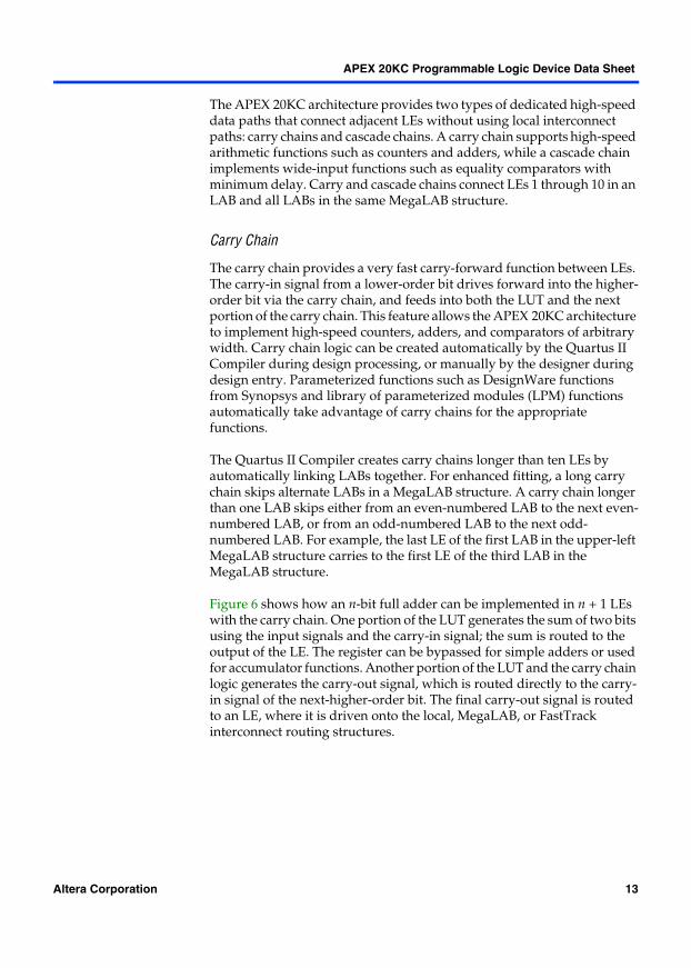
The APEX 20KC architecture provides two types of dedicated high-speed data paths that connect adjacent LEs without using local interconnect paths: carry chains and cascade chains. A carry chain supports high-speed arithmetic functions such as counters and adders, while a cascade chain implements wide-input functions such as equality comparators with minimum delay. Carry and cascade chains connect LEs 1 through 10 in an LAB and all LABs in the same MegaLAB structure.
Carry Chain
The carry chain provides a very fast carry-forward function between LEs. The carry-in signal from a lower-order bit drives forward into the higher-order bit via the carry chain, and feeds into both the LUT and the next portion of the carry chain. This feature allows the APEX 20KC architecture to implement high-speed counters, adders, and comparators of arbitrary width. Carry chain logic can be created automatically by the Quartus II Compiler during design processing, or manually by the designer during design entry. Parameterized functions such as DesignWare functions from Synopsys and library of parameterized modules (LPM) functions automatically take advantage of carry chains for the appropriate functions.
The Quartus II Compiler creates carry chains longer than ten LEs by automatically linking LABs together. For enhanced fitting, a long carry chain skips alternate LABs in a MegaLAB structure. A carry chain longer than one LAB skips either from an even-numbered LAB to the next even-numbered LAB, or from an odd-numbered LAB to the next odd-numbered LAB. For example, the last LE of the first LAB in the upper-left MegaLAB structure carries to the first LE of the third LAB in the MegaLAB structure.
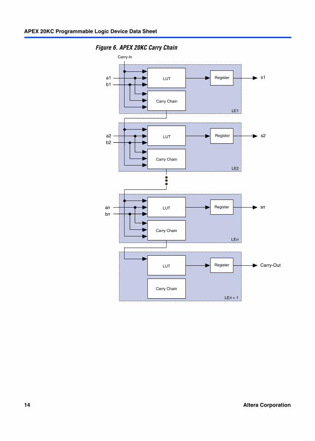
Figure 6 shows how an n-bit full adder can be implemented in n + 1 LEs with the carry chain. One portion of the LUT generates the sum of two bits using the input signals and the carry-in signal; the sum is routed to the output of the LE. The register can be bypassed for simple adders or used for accumulator functions. Another portion of the LUT and the carry chain logic generates the carry-out signal, which is routed directly to the carry-in signal of the next-higher-order bit. The final carry-out signal is routed to an LE, where it is driven onto the local, MegaLAB, or FastTrack interconnect routing structures.
Altera Corporation 13
APEX 20KC Programmable Logic Device Data Sheet
Figure 6. APEX 20KC Carry Chain
LUTa1b1
Carry Chain
s1
LE1
Register
a2b2
Carry Chain
s2
LE2
Register
Carry Chain
sn
LEn
Registeranbn
Carry Chain
Carry-Out
LEn + 1
Register
Carry-In
LUT
LUT
LUT
14 Altera Corporation
APEX 20KC Programmable Logic Device Data Sheet
Cascade Chain
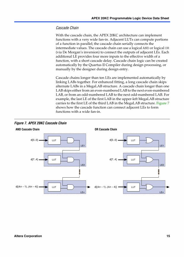
With the cascade chain, the APEX 20KC architecture can implement functions with a very wide fan-in. Adjacent LUTs can compute portions of a function in parallel; the cascade chain serially connects the intermediate values. The cascade chain can use a logical AND or logical OR (via De Morgan’s inversion) to connect the outputs of adjacent LEs. Each additional LE provides four more inputs to the effective width of a function, with a short cascade delay. Cascade chain logic can be created automatically by the Quartus II Compiler during design processing, or manually by the designer during design entry.
Cascade chains longer than ten LEs are implemented automatically by linking LABs together. For enhanced fitting, a long cascade chain skips alternate LABs in a MegaLAB structure. A cascade chain longer than one LAB skips either from an even-numbered LAB to the next even-numbered LAB, or from an odd-numbered LAB to the next odd-numbered LAB. For example, the last LE of the first LAB in the upper-left MegaLAB structure carries to the first LE of the third LAB in the MegaLAB structure. Figure 7 shows how the cascade function can connect adjacent LEs to form functions with a wide fan-in.
Figure 7. APEX 20KC Cascade Chain
LE1
LUT
LE2
LUT
d[3..0]
d[7..4]
d[(4n – 1)..(4n – 4)]
d[3..0]
d[7..4]
LEn
LE1
LE2
LEn
LUT
LUT
LUT
LUT
AND Cascade Chain OR Cascade Chain
d[(4n – 1)..(4n – 4)]
Altera Corporation 15
APEX 20KC Programmable Logic Device Data Sheet
LE Operating Modes
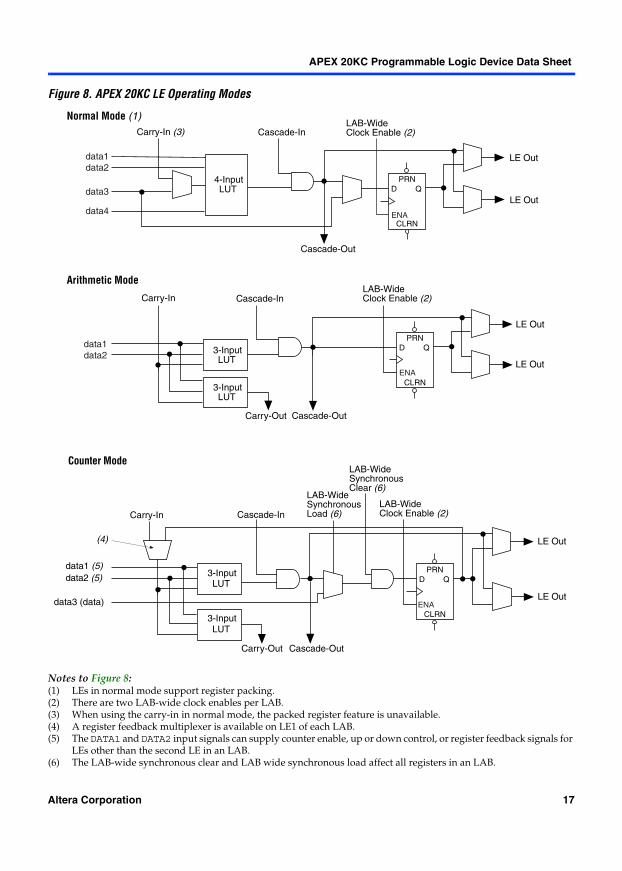
The APEX 20KC LE can operate in one of the following three modes:
Normal mode Arithmetic mode Counter mode
Each mode uses LE resources differently. In each mode, seven available inputs to the LE—the four data inputs from the LAB local interconnect, the feedback from the programmable register, and the carry-in and cascade-in from the previous LE—are directed to different destinations to implement the desired logic function. LAB-wide signals provide clock, asynchronous clear, asynchronous preset, asynchronous load, synchronous clear, synchronous load, and clock enable control for the register. These LAB-wide signals are available in all LE modes.
The Quartus II software, in conjunction with parameterized functions such as LPM and DesignWare functions, automatically chooses the appropriate mode for common functions such as counters, adders, and multipliers. If required, the designer can also create special-purpose functions that specify which LE operating mode to use for optimal performance. Figure 8 shows the LE operating modes.
16 Altera Corporation
APEX 20KC Programmable Logic Device Data Sheet
Figure 8. APEX 20KC LE Operating Modes
Notes to Figure 8:(1) LEs in normal mode support register packing.(2) There are two LAB-wide clock enables per LAB.(3) When using the carry-in in normal mode, the packed register feature is unavailable.(4) A register feedback multiplexer is available on LE1 of each LAB.(5) The DATA1 and DATA2 input signals can supply counter enable, up or down control, or register feedback signals for
LEs other than the second LE in an LAB.(6) The LAB-wide synchronous clear and LAB wide synchronous load affect all registers in an LAB.
PRN
CLRN
D Q4-InputLUT
Carry-In (3)
Cascade-Out
Cascade-In
LE Out
Normal Mode (1)
PRN
CLRN
D Q
Cascade-Out
Cascade-In
3-InputLUT
Carry-In
3-InputLUT
Carry-Out
Arithmetic Mode
Counter Mode
data1 (5)data2 (5)
PRN
CLRN
D Q
Carry-In
LUT
3-Input
3-Input
LUT
Carry-Out
data3 (data)
Cascade-Out
Cascade-In
LAB-WideSynchronous Load (6)
LAB-Wide Synchronous Clear (6)
(4)
LE Out
LE Out
LE Out
LE Out
LE Out ENA
LAB-Wide Clock Enable (2)
ENA
LAB-Wide Clock Enable (2)
ENA
LAB-Wide Clock Enable (2)
data1data2
data1data2
data3
data4
Altera Corporation 17
APEX 20KC Programmable Logic Device Data Sheet
Normal Mode
The normal mode is suitable for general logic applications, combinatorial functions, or wide decoding functions that can take advantage of a cascade chain. In normal mode, four data inputs from the LAB local interconnect and the carry-in are inputs to a four-input LUT. The Quartus II Compiler automatically selects the carry-in or the DATA3 signal as one of the inputs to the LUT. The LUT output can be combined with the cascade-in signal to form a cascade chain through the cascade-out signal. LEs in normal mode support packed registers.
Arithmetic Mode
The arithmetic mode is ideal for implementing adders, accumulators, and comparators. An LE in arithmetic mode uses two 3-input LUTs. One LUT computes a three-input function; the other generates a carry output. As shown in Figure 8, the first LUT uses the carry-in signal and two data inputs from the LAB local interconnect to generate a combinatorial or registered output. For example, when implementing an adder, this output is the sum of three signals: DATA1, DATA2, and carry-in. The second LUT uses the same three signals to generate a carry-out signal, thereby creating a carry chain. The arithmetic mode also supports simultaneous use of the cascade chain. LEs in arithmetic mode can drive out registered and unregistered versions of the LUT output.
The Quartus II software implements parameterized functions that use the arithmetic mode automatically where appropriate; the designer does not need to specify how the carry chain will be used.
Counter Mode
The counter mode offers clock enable, counter enable, synchronous up/down control, synchronous clear, and synchronous load options. The counter enable and synchronous up/down control signals are generated from the data inputs of the LAB local interconnect. The synchronous clear and synchronous load options are LAB-wide signals that affect all registers in the LAB. Consequently, if any of the LEs in an LAB use the counter mode, other LEs in that LAB must be used as part of the same counter or be used for a combinatorial function. The Quartus II software automatically places any registers that are not used by the counter into other LABs.
18 Altera Corporation
APEX 20KC Programmable Logic Device Data Sheet
The counter mode uses two 3-input LUTs: one generates the counter data, and the other generates the fast carry bit. A 2-to-1 multiplexer provides synchronous loading, and another AND gate provides synchronous clearing. If the cascade function is used by an LE in counter mode, the synchronous clear or load overrides any signal carried on the cascade chain. The synchronous clear overrides the synchronous load. LEs in arithmetic mode can drive out registered and unregistered versions of the LUT output.
Clear & Preset Logic Control
Logic for the register’s clear and preset signals is controlled by LAB-wide signals. The LE directly supports an asynchronous clear function. The Quartus II Compiler can use a NOT-gate push-back technique to emulate an asynchronous preset or to emulate simultaneous preset and clear or asynchronous load. However, this technique uses three additional LEs per register. All emulation is performed automatically when the design is compiled. Registers that emulate simultaneous preset and load will enter an unknown state upon power-up or when the chip-wide reset is asserted.
In addition to the two clear and preset modes, APEX 20KC devices provide a chip-wide reset pin (DEV_CLRn) that resets all registers in the device. Use of this pin is controlled through an option in the Quartus II software that is set before compilation. The chip-wide reset overrides all other control signals. Registers using an asynchronous preset are preset when the chip-wide reset is asserted; this effect results from the inversion technique used to implement the asynchronous preset.
FastTrack Interconnect
In the APEX 20KC architecture, connections between LEs, ESBs, and I/O pins are provided by the FastTrack interconnect. The FastTrack interconnect is a series of continuous horizontal and vertical routing channels that traverse the device. This global routing structure provides predictable performance, even in complex designs. In contrast, the segmented routing in FPGAs requires switch matrices to connect a variable number of routing paths, increasing the delays between logic resources and reducing performance.
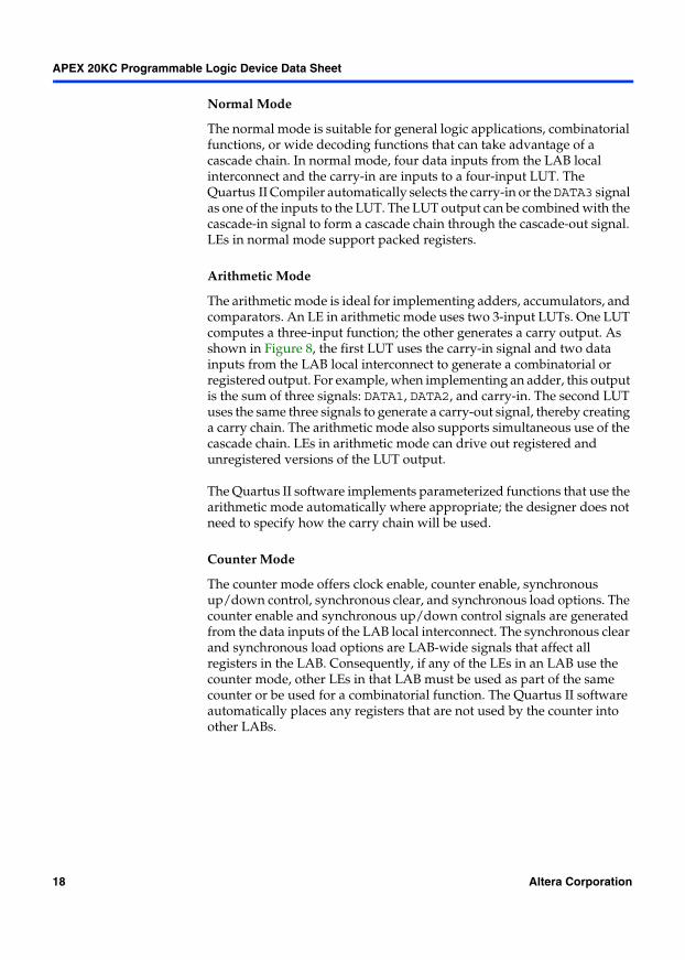
The FastTrack interconnect consists of row and column interconnect channels that span the entire device. The row interconnect routes signals throughout a row of MegaLAB structures; the column interconnect routes signals throughout a column of MegaLAB structures. When using the row and column interconnect, an LE, IOE, or ESB can drive any other LE, IOE, or ESB in a device. See Figure 9.
Altera Corporation 19
APEX 20KC Programmable Logic Device Data Sheet
Figure 9. APEX 20KC Interconnect Structure
A row line can be driven directly by LEs, IOEs, or ESBs in that row. Further, a column line can drive a row line, allowing an LE, IOE, or ESB to drive elements in a different row via the column and row interconnect. The row interconnect drives the MegaLAB interconnect to drive LEs, IOEs, or ESBs in a particular MegaLAB structure.
A column line can be directly driven by LEs, IOEs, or ESBs in that column. A column line on a device’s left or right edge can also be driven by row IOEs. The column line is used to route signals from one row to another. A column line can drive a row line; it can also drive the MegaLAB interconnect directly, allowing faster connections between rows.
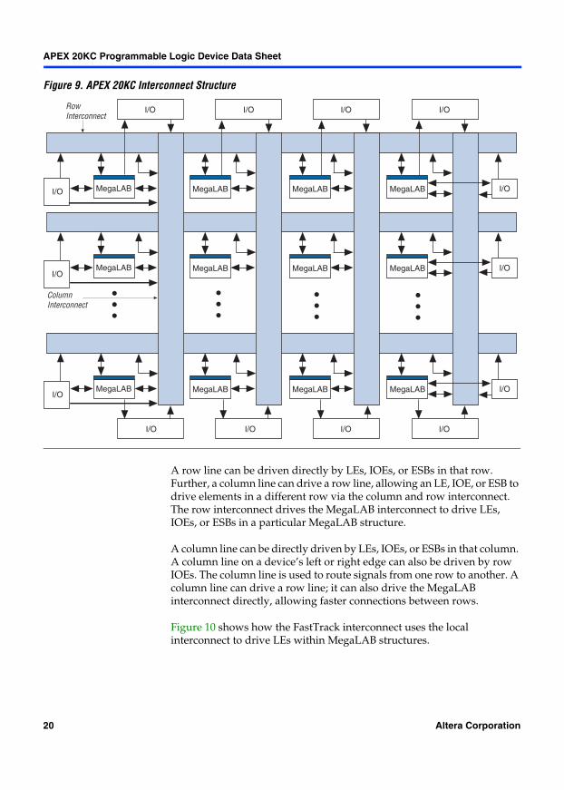
Figure 10 shows how the FastTrack interconnect uses the local interconnect to drive LEs within MegaLAB structures.
MegaLAB MegaLAB MegaLAB MegaLAB I/O
I/O I/OI/OI/O
I/O
I/O
I/O
MegaLAB MegaLAB MegaLAB MegaLAB I/O
MegaLAB MegaLAB MegaLAB MegaLAB I/O
I/O I/OI/OI/O
Column Interconnect
Row Interconnect
20 Altera Corporation
APEX 20KC Programmable Logic Device Data Sheet
Figure 10. FastTrack Connection to Local Interconnect
LAB
LAB
LAB
LAB
ESB
LAB
LAB
I/O
I/O
MegaLABStructure Column
Row
MegaLABStructure
MegaLABInterconnect
Row & ColumnInterconnect DrivesMegaLAB Interconnect
MegaLAB Interconnect DrivesLocal Interconnect
LAB
LAB
LAB
ESB
Row
Column
ESB
Altera Corporation 21
APEX 20KC Programmable Logic Device Data Sheet
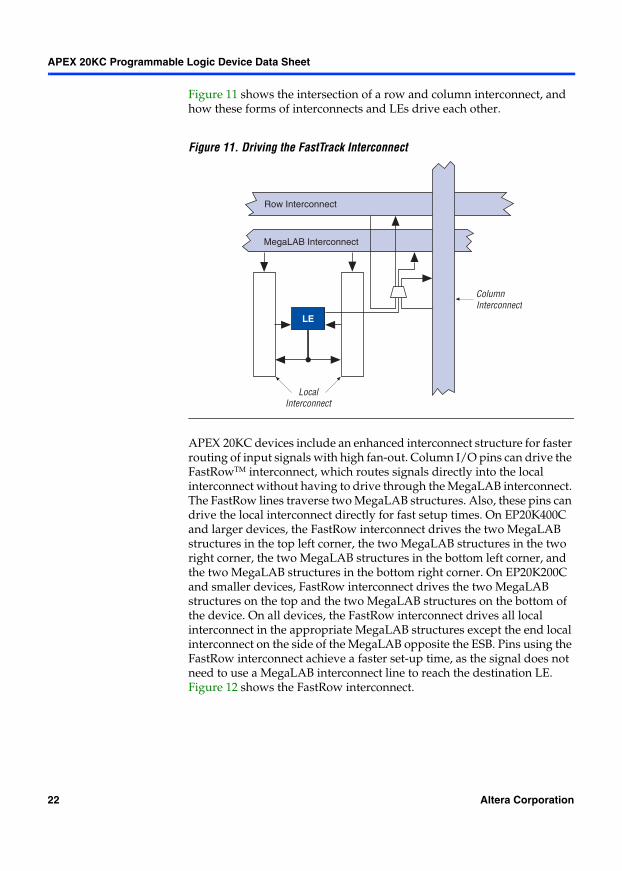
Figure 11 shows the intersection of a row and column interconnect, and how these forms of interconnects and LEs drive each other.
Figure 11. Driving the FastTrack Interconnect
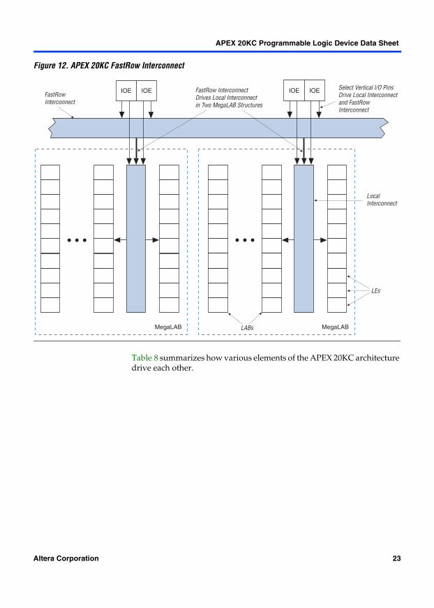
APEX 20KC devices include an enhanced interconnect structure for faster routing of input signals with high fan-out. Column I/O pins can drive the FastRowTM interconnect, which routes signals directly into the local interconnect without having to drive through the MegaLAB interconnect. The FastRow lines traverse two MegaLAB structures. Also, these pins can drive the local interconnect directly for fast setup times. On EP20K400C and larger devices, the FastRow interconnect drives the two MegaLAB structures in the top left corner, the two MegaLAB structures in the two right corner, the two MegaLAB structures in the bottom left corner, and the two MegaLAB structures in the bottom right corner. On EP20K200C and smaller devices, FastRow interconnect drives the two MegaLAB structures on the top and the two MegaLAB structures on the bottom of the device. On all devices, the FastRow interconnect drives all local interconnect in the appropriate MegaLAB structures except the end local interconnect on the side of the MegaLAB opposite the ESB. Pins using the FastRow interconnect achieve a faster set-up time, as the signal does not need to use a MegaLAB interconnect line to reach the destination LE. Figure 12 shows the FastRow interconnect.
Row Interconnect
MegaLAB Interconnect
LE
ColumnInterconnect
LocalInterconnect
22 Altera Corporation
APEX 20KC Programmable Logic Device Data Sheet
Figure 12. APEX 20KC FastRow Interconnect
Table 8 summarizes how various elements of the APEX 20KC architecture drive each other.
IOE IOE IOE IOEFastRow InterconnectDrives Local Interconnectin Two MegaLAB Structures
MegaLAB MegaLAB
LocalInterconnect
Select Vertical I/O Pins Drive Local Interconnectand FastRowInterconnect
FastRowInterconnect
LEs
LABs
Altera Corporation 23
APEX 20KC Programmable Logic Device Data Sheet
Product-Term Logic
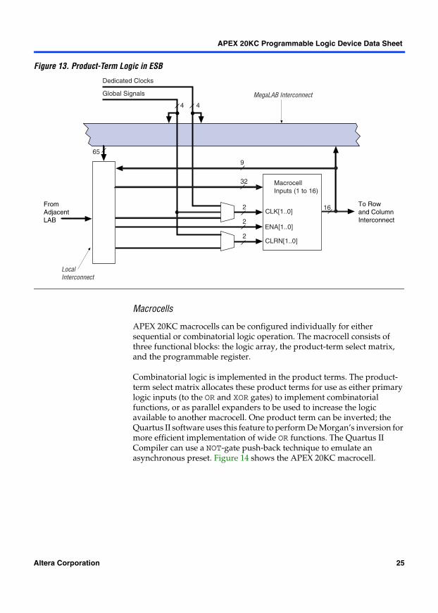
The product-term portion of the MultiCore architecture is implemented with the ESB. The ESB can be configured to act as a block of macrocells on an ESB-by-ESB basis. Each ESB is fed by 32 inputs from the adjacent local interconnect; therefore, it can be driven by the MegaLAB interconnect or the adjacent LAB. Also, nine ESB macrocells feed back into the ESB through the local interconnect for higher performance. Dedicated clock pins, global signals, and additional inputs from the local interconnect drive the ESB control signals.
In product-term mode, each ESB contains 16 macrocells. Each macrocell consists of two product terms and a programmable register. Figure 13 shows the ESB in product-term mode.
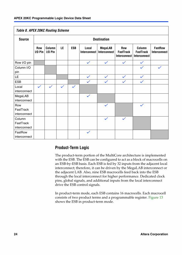
Table 8. APEX 20KC Routing Scheme
Source Destination
Row I/O Pin
Column I/O Pin
LE ESB Local Interconnect
MegaLAB Interconnect
Row FastTrack
Interconnect
Column FastTrack
Interconnect
FastRow Interconnect
Row I/O pin v v v v
Column I/O pin
v v
LE v v v v
ESB v v v v
Local interconnect
v v v v
MegaLAB interconnect
v
Row FastTrack interconnect
v v
Column FastTrack interconnect
v v
FastRow interconnect
v
24 Altera Corporation
APEX 20KC Programmable Logic Device Data Sheet
Figure 13. Product-Term Logic in ESB
Macrocells
APEX 20KC macrocells can be configured individually for either sequential or combinatorial logic operation. The macrocell consists of three functional blocks: the logic array, the product-term select matrix, and the programmable register.
Combinatorial logic is implemented in the product terms. The product-term select matrix allocates these product terms for use as either primary logic inputs (to the OR and XOR gates) to implement combinatorial functions, or as parallel expanders to be used to increase the logic available to another macrocell. One product term can be inverted; the Quartus II software uses this feature to perform De Morgan’s inversion for more efficient implementation of wide OR functions. The Quartus II Compiler can use a NOT-gate push-back technique to emulate an asynchronous preset. Figure 14 shows the APEX 20KC macrocell.
Global Signals
Dedicated Clocks
MacrocellInputs (1 to 16)
CLK[1..0]
ENA[1..0]
CLRN[1..0]
From Adjacent LAB
MegaLAB Interconnect
To Row and Column Interconnect
2 16
32
2
2
4 4
65
Local Interconnect
9
Altera Corporation 25
APEX 20KC Programmable Logic Device Data Sheet
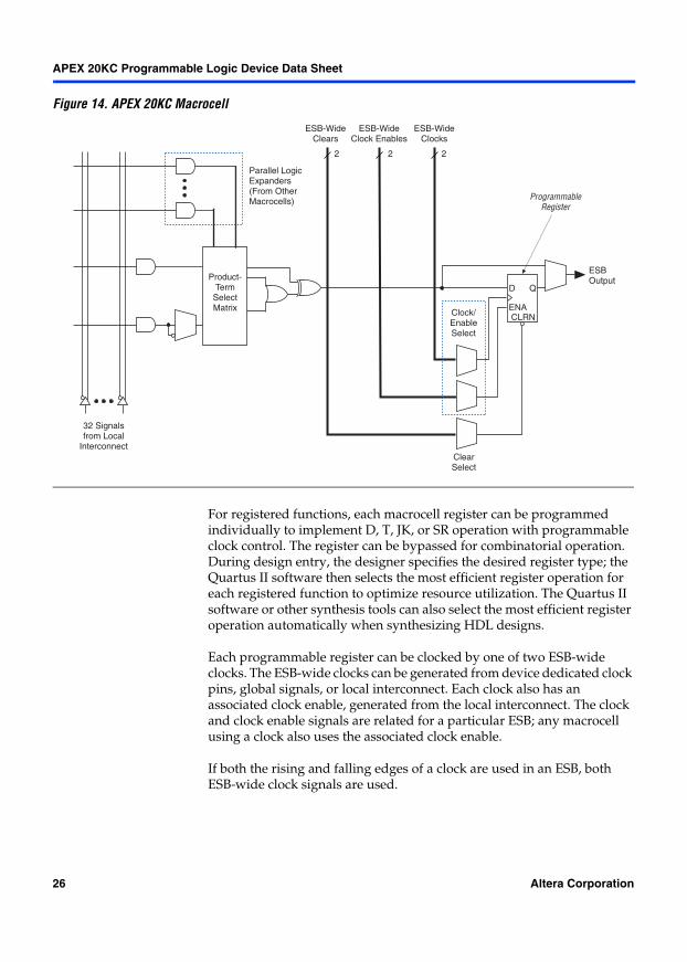
Figure 14. APEX 20KC Macrocell
For registered functions, each macrocell register can be programmed individually to implement D, T, JK, or SR operation with programmable clock control. The register can be bypassed for combinatorial operation. During design entry, the designer specifies the desired register type; the Quartus II software then selects the most efficient register operation for each registered function to optimize resource utilization. The Quartus II software or other synthesis tools can also select the most efficient register operation automatically when synthesizing HDL designs.
Each programmable register can be clocked by one of two ESB-wide clocks. The ESB-wide clocks can be generated from device dedicated clock pins, global signals, or local interconnect. Each clock also has an associated clock enable, generated from the local interconnect. The clock and clock enable signals are related for a particular ESB; any macrocell using a clock also uses the associated clock enable.
If both the rising and falling edges of a clock are used in an ESB, both ESB-wide clock signals are used.
Clock/EnableSelect
Product-Term
SelectMatrix
Parallel LogicExpanders(From OtherMacrocells)
ESB-WideClears
ESB-WideClock Enables
ESB-WideClocks
32 Signalsfrom Local
InterconnectClearSelect
ESB Output
ProgrammableRegister
2 2 2
ENA
D
CLRN
Q
26 Altera Corporation
APEX 20KC Programmable Logic Device Data Sheet
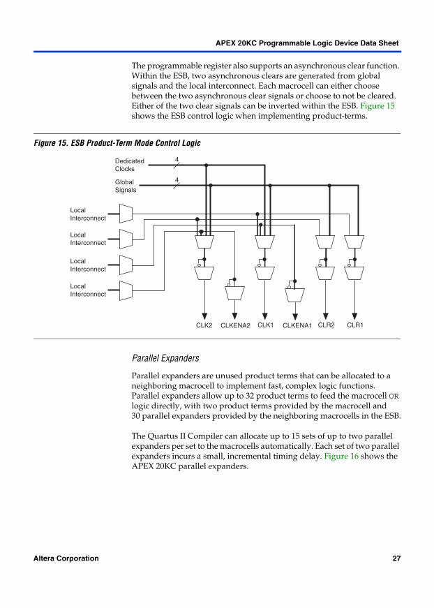
The programmable register also supports an asynchronous clear function. Within the ESB, two asynchronous clears are generated from global signals and the local interconnect. Each macrocell can either choose between the two asynchronous clear signals or choose to not be cleared. Either of the two clear signals can be inverted within the ESB. Figure 15 shows the ESB control logic when implementing product-terms.
Figure 15. ESB Product-Term Mode Control Logic
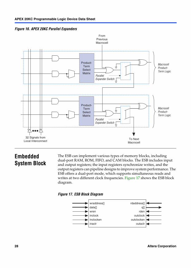
Parallel Expanders
Parallel expanders are unused product terms that can be allocated to a neighboring macrocell to implement fast, complex logic functions. Parallel expanders allow up to 32 product terms to feed the macrocell OR logic directly, with two product terms provided by the macrocell and 30 parallel expanders provided by the neighboring macrocells in the ESB.
The Quartus II Compiler can allocate up to 15 sets of up to two parallel expanders per set to the macrocells automatically. Each set of two parallel expanders incurs a small, incremental timing delay. Figure 16 shows the APEX 20KC parallel expanders.
CLK2 CLKENA2 CLK1 CLKENA1 CLR2 CLR1
DedicatedClocks
GlobalSignals
LocalInterconnect
LocalInterconnect
LocalInterconnect
LocalInterconnect
4
4
Altera Corporation 27
APEX 20KC Programmable Logic Device Data Sheet
Figure 16. APEX 20KC Parallel Expanders
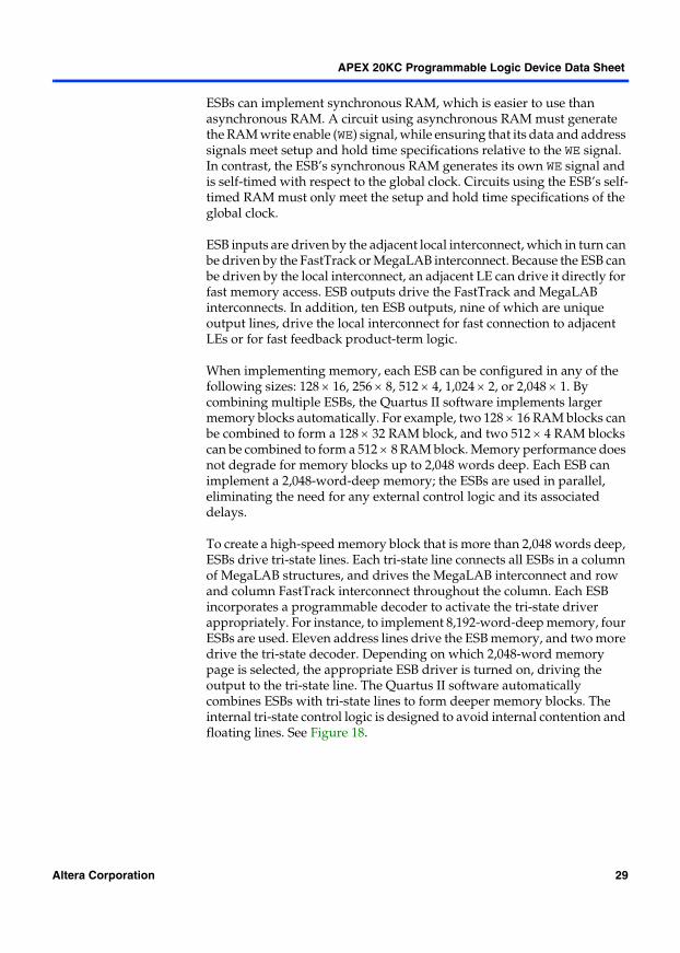
Embedded System Block
The ESB can implement various types of memory blocks, including dual-port RAM, ROM, FIFO, and CAM blocks. The ESB includes input and output registers; the input registers synchronize writes, and the output registers can pipeline designs to improve system performance. The ESB offers a dual-port mode, which supports simultaneous reads and writes at two different clock frequencies. Figure 17 shows the ESB block diagram.
Figure 17. ESB Block Diagram
32 Signals fromLocal Interconnect
To NextMacrocell
FromPreviousMacrocell
Product-TermSelectMatrix
Product-TermSelectMatrix
MacrocellProduct-Term Logic
MacrocellProduct-Term Logic
ParallelExpander Switch
ParallelExpander Switch
wraddress[]data[]wreninclockinclockeninaclr
rdaddress[]q[]
rdenoutclock
outclockenoutaclr
28 Altera Corporation
APEX 20KC Programmable Logic Device Data Sheet
ESBs can implement synchronous RAM, which is easier to use than asynchronous RAM. A circuit using asynchronous RAM must generate the RAM write enable (WE) signal, while ensuring that its data and address signals meet setup and hold time specifications relative to the WE signal. In contrast, the ESB’s synchronous RAM generates its own WE signal and is self-timed with respect to the global clock. Circuits using the ESB’s self-timed RAM must only meet the setup and hold time specifications of the global clock.
ESB inputs are driven by the adjacent local interconnect, which in turn can be driven by the FastTrack or MegaLAB interconnect. Because the ESB can be driven by the local interconnect, an adjacent LE can drive it directly for fast memory access. ESB outputs drive the FastTrack and MegaLAB interconnects. In addition, ten ESB outputs, nine of which are unique output lines, drive the local interconnect for fast connection to adjacent LEs or for fast feedback product-term logic.
When implementing memory, each ESB can be configured in any of the following sizes: 128 × 16, 256 × 8, 512 × 4, 1,024 × 2, or 2,048 × 1. By combining multiple ESBs, the Quartus II software implements larger memory blocks automatically. For example, two 128 × 16 RAM blocks can be combined to form a 128 × 32 RAM block, and two 512 × 4 RAM blocks can be combined to form a 512 × 8 RAM block. Memory performance does not degrade for memory blocks up to 2,048 words deep. Each ESB can implement a 2,048-word-deep memory; the ESBs are used in parallel, eliminating the need for any external control logic and its associated delays.
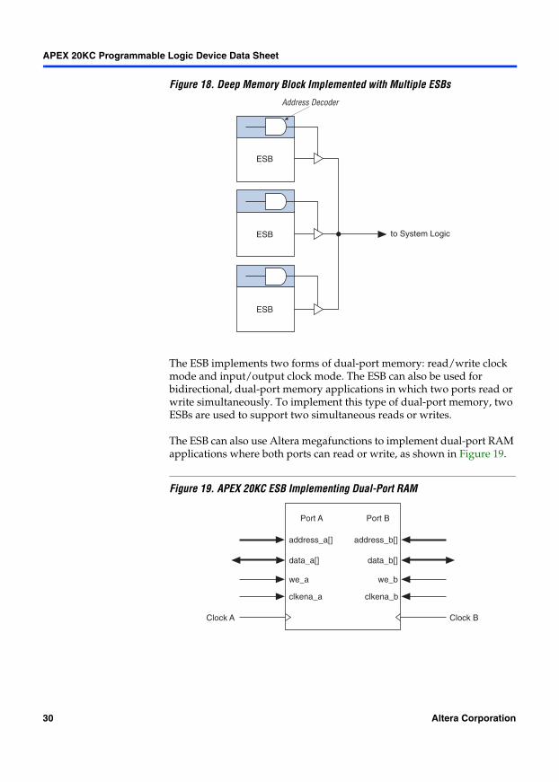
To create a high-speed memory block that is more than 2,048 words deep, ESBs drive tri-state lines. Each tri-state line connects all ESBs in a column of MegaLAB structures, and drives the MegaLAB interconnect and row and column FastTrack interconnect throughout the column. Each ESB incorporates a programmable decoder to activate the tri-state driver appropriately. For instance, to implement 8,192-word-deep memory, four ESBs are used. Eleven address lines drive the ESB memory, and two more drive the tri-state decoder. Depending on which 2,048-word memory page is selected, the appropriate ESB driver is turned on, driving the output to the tri-state line. The Quartus II software automatically combines ESBs with tri-state lines to form deeper memory blocks. The internal tri-state control logic is designed to avoid internal contention and floating lines. See Figure 18.
Altera Corporation 29
APEX 20KC Programmable Logic Device Data Sheet
Figure 18. Deep Memory Block Implemented with Multiple ESBs
The ESB implements two forms of dual-port memory: read/write clock mode and input/output clock mode. The ESB can also be used for bidirectional, dual-port memory applications in which two ports read or write simultaneously. To implement this type of dual-port memory, two ESBs are used to support two simultaneous reads or writes.
The ESB can also use Altera megafunctions to implement dual-port RAM applications where both ports can read or write, as shown in Figure 19.
Figure 19. APEX 20KC ESB Implementing Dual-Port RAM
ESB
ESB
ESB
to System Logic
Address Decoder
Port A Port B
address_a[] address_b[]
data_a[] data_b[]
we_a we_b
clkena_a clkena_b
Clock A Clock B
30 Altera Corporation
APEX 20KC Programmable Logic Device Data Sheet
Read/Write Clock Mode
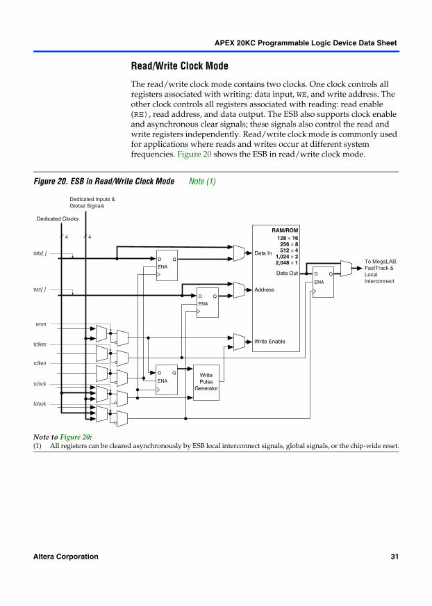
The read/write clock mode contains two clocks. One clock controls all registers associated with writing: data input, WE, and write address. The other clock controls all registers associated with reading: read enable (RE), read address, and data output. The ESB also supports clock enable and asynchronous clear signals; these signals also control the read and write registers independently. Read/write clock mode is commonly used for applications where reads and writes occur at different system frequencies. Figure 20 shows the ESB in read/write clock mode.
Figure 20. ESB in Read/Write Clock Mode Note (1)
Note to Figure 20:(1) All registers can be cleared asynchronously by ESB local interconnect signals, global signals, or the chip-wide reset.
Dedicated Clocks
4 4
D
ENA
Q
D
ENA
Q
D
ENA
Q
D
ENA
Q
data[ ]
ress[ ]
RAM/ROM128 × 16256 × 8512 × 4
1,024 × 22,048 × 1
Data In
Address
Write Enable
Data Out
utclken
nclken
nclock
utclock
WritePulse
Generator
wren
Dedicated Inputs &Global Signals
To MegaLAB,FastTrack &Local Interconnect
Altera Corporation 31
APEX 20KC Programmable Logic Device Data Sheet
Input/Output Clock Mode
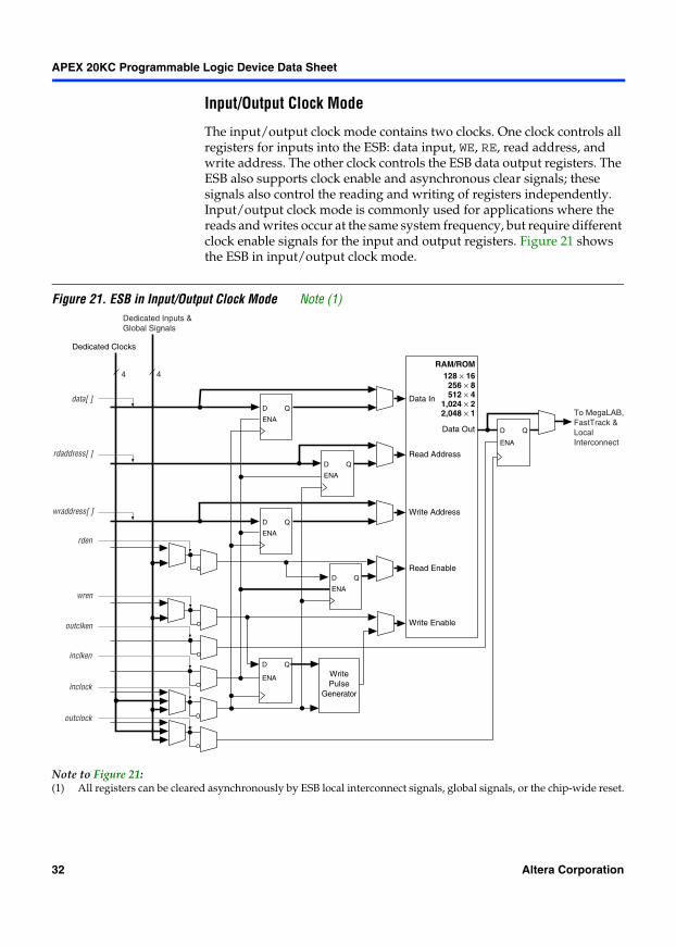
The input/output clock mode contains two clocks. One clock controls all registers for inputs into the ESB: data input, WE, RE, read address, and write address. The other clock controls the ESB data output registers. The ESB also supports clock enable and asynchronous clear signals; these signals also control the reading and writing of registers independently. Input/output clock mode is commonly used for applications where the reads and writes occur at the same system frequency, but require different clock enable signals for the input and output registers. Figure 21 shows the ESB in input/output clock mode.
Figure 21. ESB in Input/Output Clock Mode Note (1)
Note to Figure 21:(1) All registers can be cleared asynchronously by ESB local interconnect signals, global signals, or the chip-wide reset.
Dedicated Clocks
4 4
D
ENA
Q
D
ENA
Q
D
ENA
Q
D
ENA
Q
D
ENA
Q
data[ ]
rdaddress[ ]
wraddress[ ]
RAM/ROM128 × 16
256 × 8512 × 4
1,024 × 22,048 × 1
Data In
Read Address
Write Address
Read Enable
Write Enable
Data Out
outclken
inclken
inclock
outclock
D
ENA
Q
WritePulse
Generator
rden
wren
Dedicated Inputs &Global Signals
To MegaLAB,FastTrack &LocalInterconnect
32 Altera Corporation
APEX 20KC Programmable Logic Device Data Sheet
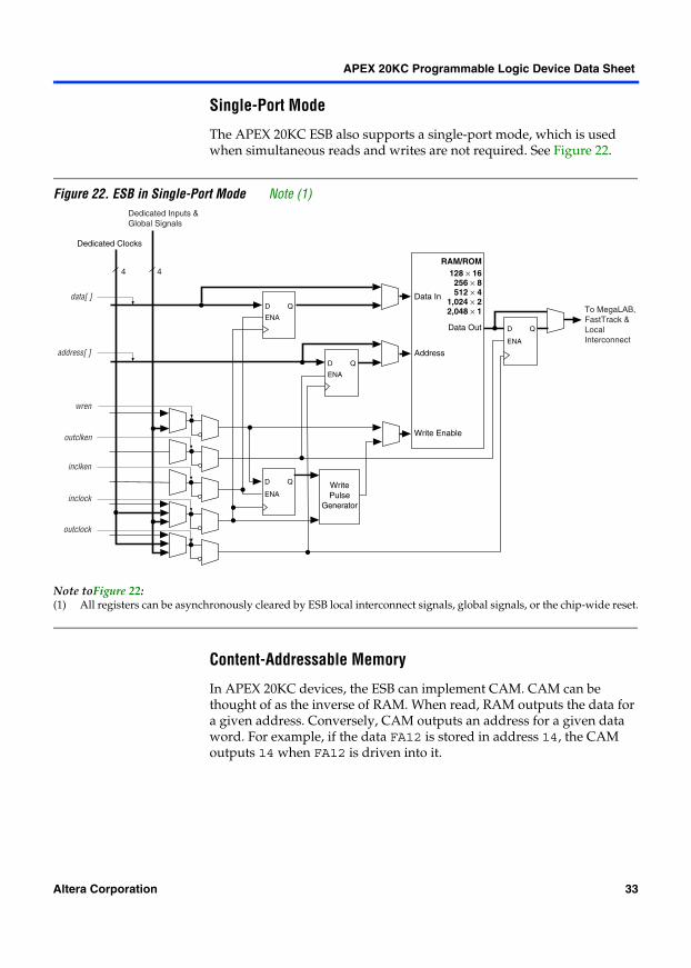
Single-Port Mode
The APEX 20KC ESB also supports a single-port mode, which is used when simultaneous reads and writes are not required. See Figure 22.
Figure 22. ESB in Single-Port Mode Note (1)
Note toFigure 22:(1) All registers can be asynchronously cleared by ESB local interconnect signals, global signals, or the chip-wide reset.
Content-Addressable Memory
In APEX 20KC devices, the ESB can implement CAM. CAM can be thought of as the inverse of RAM. When read, RAM outputs the data for a given address. Conversely, CAM outputs an address for a given data word. For example, if the data FA12 is stored in address 14, the CAM outputs 14 when FA12 is driven into it.
Dedicated Clocks
4 4
D
ENA
Q
D
ENA
Q
D
ENA
Q
D
ENA
Q
data[ ]
address[ ]
RAM/ROM128 × 16
256 × 8512 × 4
1,024 × 22,048 × 1
Data In
Address
Write Enable
Data Out
outclken
inclken
inclock
outclock
WritePulse
Generator
wren
Dedicated Inputs &Global Signals
To MegaLAB,FastTrack &Local Interconnect
Altera Corporation 33
APEX 20KC Programmable Logic Device Data Sheet
CAM is used for high-speed search operations. When searching for data within a RAM block, the search is performed serially. Thus, finding a particular data word can take many cycles. CAM searches all addresses in parallel and outputs the address storing a particular word. When a match is found, a match flag is set high. Figure 23 shows the CAM block diagram.
34 Altera Corporation
APEX 20KC Programmable Logic Device Data Sheet
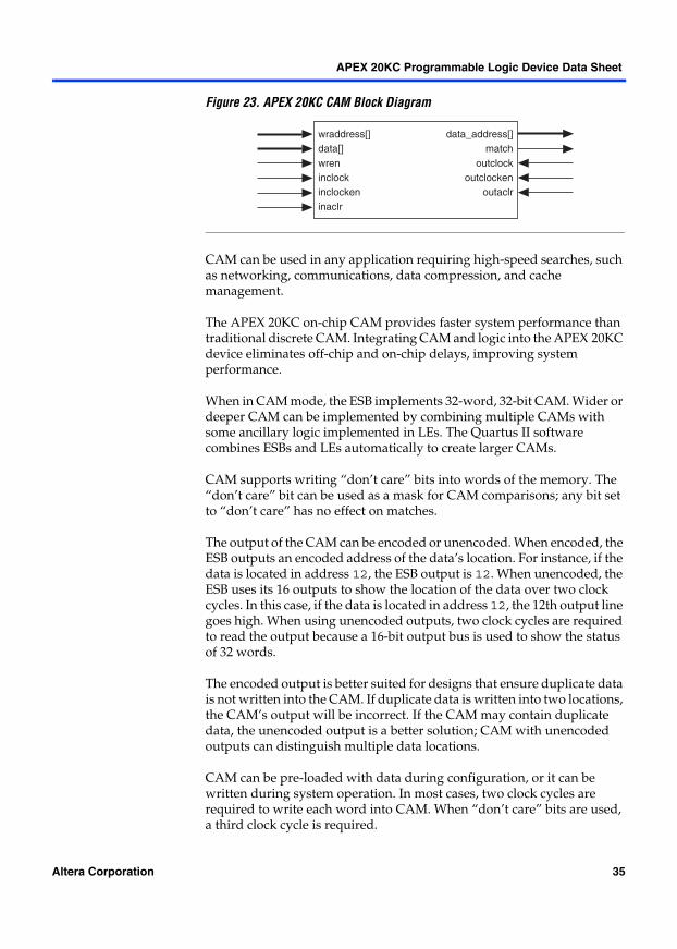
Figure 23. APEX 20KC CAM Block Diagram
CAM can be used in any application requiring high-speed searches, such as networking, communications, data compression, and cache management.
The APEX 20KC on-chip CAM provides faster system performance than traditional discrete CAM. Integrating CAM and logic into the APEX 20KC device eliminates off-chip and on-chip delays, improving system performance.
When in CAM mode, the ESB implements 32-word, 32-bit CAM. Wider or deeper CAM can be implemented by combining multiple CAMs with some ancillary logic implemented in LEs. The Quartus II software combines ESBs and LEs automatically to create larger CAMs.
CAM supports writing “don’t care” bits into words of the memory. The “don’t care” bit can be used as a mask for CAM comparisons; any bit set to “don’t care” has no effect on matches.
The output of the CAM can be encoded or unencoded. When encoded, the ESB outputs an encoded address of the data’s location. For instance, if the data is located in address 12, the ESB output is 12. When unencoded, the ESB uses its 16 outputs to show the location of the data over two clock cycles. In this case, if the data is located in address 12, the 12th output line goes high. When using unencoded outputs, two clock cycles are required to read the output because a 16-bit output bus is used to show the status of 32 words.
The encoded output is better suited for designs that ensure duplicate data is not written into the CAM. If duplicate data is written into two locations, the CAM’s output will be incorrect. If the CAM may contain duplicate data, the unencoded output is a better solution; CAM with unencoded outputs can distinguish multiple data locations.
CAM can be pre-loaded with data during configuration, or it can be written during system operation. In most cases, two clock cycles are required to write each word into CAM. When “don’t care” bits are used, a third clock cycle is required.
wraddress[]data[]wreninclockinclockeninaclr
data_address[]match
outclockoutclocken
outaclr
Altera Corporation 35
APEX 20KC Programmable Logic Device Data Sheet
f For more information on APEX 20KC devices and CAM, see Application Note 119 (Implementing High-Speed Search Applications with APEX CAM).
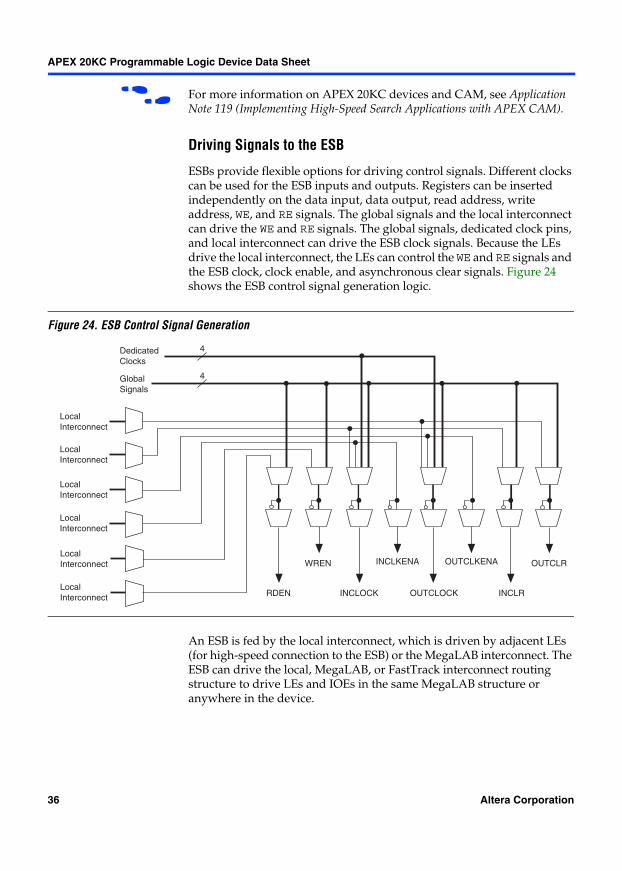
Driving Signals to the ESB
ESBs provide flexible options for driving control signals. Different clocks can be used for the ESB inputs and outputs. Registers can be inserted independently on the data input, data output, read address, write address, WE, and RE signals. The global signals and the local interconnect can drive the WE and RE signals. The global signals, dedicated clock pins, and local interconnect can drive the ESB clock signals. Because the LEs drive the local interconnect, the LEs can control the WE and RE signals and the ESB clock, clock enable, and asynchronous clear signals. Figure 24 shows the ESB control signal generation logic.
Figure 24. ESB Control Signal Generation
An ESB is fed by the local interconnect, which is driven by adjacent LEs (for high-speed connection to the ESB) or the MegaLAB interconnect. The ESB can drive the local, MegaLAB, or FastTrack interconnect routing structure to drive LEs and IOEs in the same MegaLAB structure or anywhere in the device.
RDEN
WREN
INCLOCK
INCLKENA
OUTCLOCK
OUTCLKENA
DedicatedClocks
GlobalSignals
LocalInterconnect
LocalInterconnect
LocalInterconnect
LocalInterconnect
4
4
LocalInterconnect
LocalInterconnect INCLR
OUTCLR
36 Altera Corporation
APEX 20KC Programmable Logic Device Data Sheet
Implementing Logic in ROM
In addition to implementing logic with product terms, the ESB can implement logic functions when it is programmed with a read-only pattern during configuration, creating a large LUT. With LUTs, combinatorial functions are implemented by looking up the results, rather than by computing them. This implementation of combinatorial functions can be faster than using algorithms implemented in general logic, a performance advantage that is further enhanced by the fast access times of ESBs. The large capacity of ESBs enables designers to implement complex functions in one logic level without the routing delays associated with linked LEs or distributed RAM blocks. Parameterized functions such as LPM functions can take advantage of the ESB automatically. Further, the Quartus II software can implement portions of a design with ESBs where appropriate.
Programmable Speed/Power Control
APEX 20KC ESBs offer a high-speed mode that supports very fast operation on an ESB-by-ESB basis. When high speed is not required, this feature can be turned off to reduce the ESB’s power dissipation by up to 50%. ESBs that run at low power incur a nominal timing delay adder. This Turbo BitTM option is available for ESBs that implement product-term logic or memory functions. An ESB that is not used will be powered down so that it does not consume DC current.
Designers can program each ESB in the APEX 20KC device for either high-speed or low-power operation. As a result, speed-critical paths in the design can run at high speed, while the remaining paths operate at reduced power.
I/O Structure The APEX 20KC IOE contains a bidirectional I/O buffer and a register that can be used either as an input register for external data requiring fast setup times or as an output register for data requiring fast clock-to-output performance. IOEs can be used as input, output, or bidirectional pins.
Altera Corporation 37
APEX 20KC Programmable Logic Device Data Sheet
APEX 20KC devices include an enhanced IOE, which drives the FastRow interconnect. The FastRow interconnect connects a column I/O pin directly to the LAB local interconnect within two MegaLAB structures. This feature provides fast setup times for pins that drive high fan-outs with complex logic, such as PCI designs. For fast bidirectional I/O timing, LE registers using local routing can improve setup times and OE timing. The APEX 20KC IOE also includes direct support for open-drain operation, giving faster clock-to-output for open-drain signals. Some programmable delays in the APEX 20KC IOE offer multiple levels of delay to fine-tune setup and hold time requirements. The Quartus II Compiler sets these delays by default to minimize setup time while providing a zero hold time.
The Quartus II Compiler uses the programmable inversion option to invert signals from the row and column interconnect automatically where appropriate. Because the APEX 20KC IOE offers one output enable per pin, the Quartus II Compiler can emulate open-drain operation efficiently.
The APEX 20KC IOE includes programmable delays that can be activated to ensure zero hold times, minimum clock-to-output times, input IOE register-to-core register transfers, or core-to-output IOE register transfers. A path in which a pin directly drives a register may require the delay to ensure zero hold time, whereas a path in which a pin drives a register through combinatorial logic may not require the delay.
Table 9 describes the APEX 20KC programmable delays and their logic options in the Quartus II software.
The Quartus II Compiler can program these delays automatically to minimize setup time while providing a zero hold time.
Table 9. APEX 20KC Programmable Delay Chains
Programmable Delay Quartus II Logic Option
Input pin to core delay Decrease input delay to internal cells
Input pin to input register delay Decrease input delay to input registers
Core to output register delay Decrease input delay to output register
Output register tCO delay Increase delay to output pin
Clock enable delay Increase clock enable delay
38 Altera Corporation
APEX 20KC Programmable Logic Device Data Sheet
The register in the APEX 20KC IOE can be programmed to power-up high or low after configuration is complete. If it is programmed to power-up low, an asynchronous clear can control the register. If it is programmed to power-up high, an asynchronous preset can control the register. This feature is useful for cases where the APEX 20KC device controls an active-low input or another device; it prevents inadvertent activation of the input upon power-up.
Figure 25 shows how fast bidirectional I/O pins are implemented in APEX 20KC devices. This feature is useful for cases where the APEX 20KC device controls an active-low input or another device; it prevents inadvertent activation of the input upon power-up.
Altera Corporation 39
APEX 20KC Programmable Logic Device Data Sheet
Figure 25. APEX 20KC Bidirectional I/O Registers Notes (1), (2)
VCC
OE[7..0]
CLK[1..0]
ENA[5..0]
CLRn[1..0]
Peripheral ControlBus
CLRN/PRN
D Q
ENA
VCC
4 DedicatedClock Inputs
Chip-WideOutput Enable
CLK[3..0]
4
12
VCC
VCC
Chip-WideReset
Input Pin to Core Delay (1)
Slew-RateControl
Open-DrainOutput
VCCIO
OptionalPCI Clamp
Output Registert Delay
Core to OutputRegister Delay
Input Pin to InputRegister Delay
CLRN
D Q
ENA
VCC
Chip-WideReset
Input Register
Output Register
CLRN
D Q
ENA
Chip-Wide Reset
VCC
OE Register
VCC
4 DedicatedInputs
Row, Column, FastRow,or Local Interconnect
Clock Enable Delay (1)
Input Pin to Core Delay (1)
CO
Input Pin to Core Delay (1)
40 Altera Corporation
APEX 20KC Programmable Logic Device Data Sheet
Notes to Figure 25:(1) This programmable delay has four settings: off and three levels of delay. (2) The output enable and input registers are LE registers in the LAB adjacent to the bidirectional pin.
Each IOE drives a row, column, MegaLAB, or local interconnect when used as an input or bidirectional pin. A row IOE can drive a local, MegaLAB, row, and column interconnect; a column IOE can drive the column interconnect. Figure 26 shows how a row IOE connects to the interconnect.
Figure 26. Row IOE Connection to the Interconnect
Row Interconnect MegaLAB Interconnect
Any LE can drive a pin through the row, column, and MegaLAB interconnect.
An LE can drive a pin through the local interconnect for faster clock-to-output times.
IOE
IOE
Each IOE can drive local, MegaLAB, row, and column interconnect. Each IOE data and OE signal is driven by the local interconnect.
LAB
Altera Corporation 41
APEX 20KC Programmable Logic Device Data Sheet
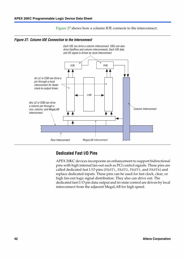
Figure 27 shows how a column IOE connects to the interconnect.
Figure 27. Column IOE Connection to the Interconnect
Dedicated Fast I/O Pins
APEX 20KC devices incorporate an enhancement to support bidirectional pins with high internal fan-out such as PCI control signals. These pins are called dedicated fast I/O pins (FAST1, FAST2, FAST3, and FAST4) and replace dedicated inputs. These pins can be used for fast clock, clear, or high fan-out logic signal distribution. They also can drive out. The dedicated fast I/O pin data output and tri-state control are driven by local interconnect from the adjacent MegaLAB for high speed.
Row Interconnect
Column Interconnect
Each IOE can drive a column interconnect. IOEs can alsodrive FastRow and column interconnects. Each IOE data and OE signal is driven by local interconnect.
Any LE or ESB can drive a column pin through a row, column, and MegaLABinterconnect.
IOE IOE
LAB
An LE or ESB can drive a pin through a local interconnect for faster clock-to-output times.
MegaLAB Interconnect
42 Altera Corporation
APEX 20KC Programmable Logic Device Data Sheet
Advanced I/O Standard Support
APEX 20KC IOEs support the following I/O standards: LVTTL, LVCMOS, 1.8-V I/O, 2.5-V I/O, 3.3-V PCI, PCI-X, 3.3-V AGP, LVDS, LVPECL, GTL+, CTT, HSTL Class I, SSTL-3 Class I and II, and SSTL-2 Class I and II.
f For more information on I/O standards supported by APEX 20KC devices, see Application Note 117 (Using Selectable I/O Standards in Altera Devices).
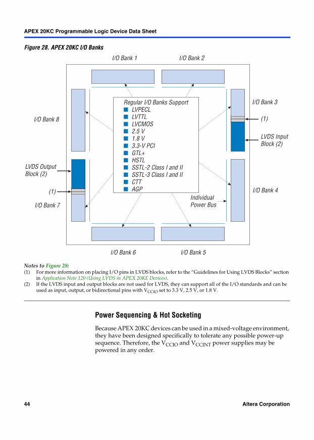
The APEX 20KC device contains eight I/O banks. In QFP packages, the banks are linked to form four I/O banks. The I/O banks directly support all standards except LVDS and LVPECL. All I/O banks can support LVDS and LVPECL at up to 156 Mbps per channel with the addition of external resistors. In addition, one block within a bank contains circuitry to support high-speed True-LVDS and LVPECL inputs, and another block within a bank supports high-speed True-LVDS and LVPECL outputs. The LVDS blocks support all of the I/O standards. Each I/O bank has its own VCCIO pins. A single device can support 1.8-V, 2.5-V, and 3.3-V interfaces; each bank can support a different standard independently. Each bank can also use a separate VREF level so that each bank can support any of the terminated standards (such as SSTL-3) independently. Within a bank, any one of the terminated standards can be supported. EP20K400C and larger APEX 20KC devices support the LVDS interface for data pins (EP20K200C devices support LVDS clock pins, but not data pins). EP20K400C and EP20K600C devices support LVDS for data pins at up to 840 Mbps per channel. EP20K1000C devices support LVDS on 16 channels at up to 750 Mbps.
Each bank can support multiple standards with the same VCCIO for output pins. Each bank can support one voltage-referenced I/O standard, but it can support multiple I/O standards with the same VCCIO voltage level. For example, when VCCIO is 3.3 V, a bank can support LVTTL, LVCMOS, 3.3-V PCI, and SSTL-3 for inputs and outputs.
When the LVDS banks are not used for the LVDS I/O standard, they support all of the other I/O standards. Figure 28 shows the arrangement of the APEX 20KC I/O banks.
Altera Corporation 43
APEX 20KC Programmable Logic Device Data Sheet
Figure 28. APEX 20KC I/O Banks
Notes to Figure 28:(1) For more information on placing I/O pins in LVDS blocks, refer to the “Guidelines for Using LVDS Blocks” section
in Application Note 120 (Using LVDS in APEX 20KE Devices).(2) If the LVDS input and output blocks are not used for LVDS, they can support all of the I/O standards and can be
used as input, output, or bidirectional pins with VCCIO set to 3.3 V, 2.5 V, or 1.8 V.
Power Sequencing & Hot Socketing
Because APEX 20KC devices can be used in a mixed-voltage environment, they have been designed specifically to tolerate any possible power-up sequence. Therefore, the VCCIO and VCCINT power supplies may be powered in any order.
LVDS InputBlock (2)
(1)
LVDS OutputBlock (2)
(1)IndividualPower Bus
I/O Bank 8
I/O Bank 1 I/O Bank 2
I/O Bank 3
I/O Bank 4
I/O Bank 5I/O Bank 6
I/O Bank 7
Regular I/O Banks Support LVPECL LVTTL LVCMOS 2.5 V 1.8 V 3.3-V PCI GTL+ HSTL SSTL-2 Class I and II SSTL-3 Class I and II CTT AGP
44 Altera Corporation
APEX 20KC Programmable Logic Device Data Sheet
Signals can be driven into APEX 20KC devices before and during power-up without damaging the device. In addition, APEX 20KC devices do not drive out during power-up. Once operating conditions are reached and the device is configured, APEX 20KC devices operate as specified by the user.
MultiVolt I/O Interface
The APEX architecture supports the MultiVolt I/O interface feature, which allows APEX devices in all packages to interface with systems of different supply voltages. The devices have one set of VCC pins for internal operation and input buffers (VCCINT), and another set for I/O output drivers (VCCIO).
APEX 20KC devices support the MultiVolt I/O interface feature. The APEX 20KC VCCINT pins must always be connected to a 1.8-V power supply. With a 1.8-V VCCINT level, input pins are 1.8-V, 2.5-V, and 3.3-V tolerant. The VCCIO pins can be connected to either a 1.8-V, 2.5-V, or 3.3-V power supply, depending on the I/O standard requirements. When the VCCIO pins are connected to a 1.8-V power supply, the output levels are compatible with 1.8-V systems. When VCCIO pins are connected to a 2.5-V power supply, the output levels are compatible with 2.5-V systems. When VCCIO pins are connected to a 3.3-V power supply, the output high is 3.3 V and compatible with 3.3-V or 5.0-V systems. An APEX 20KC device is 5.0-V tolerant with the addition of a resistor and the PCI clamp diode enabled.
f For more information on 5.0-V tolerance, refer to the “5.0-V Tolerance in APEX 20KE Devices White Paper,” as the information found therein also applies to APEX 20KC devices.
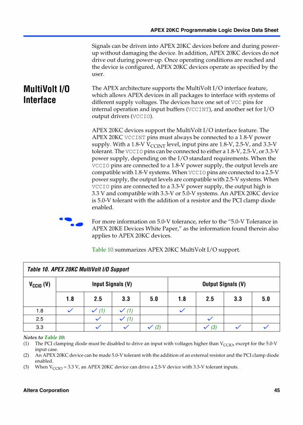
Table 10 summarizes APEX 20KC MultiVolt I/O support.
Notes to Table 10:(1) The PCI clamping diode must be disabled to drive an input with voltages higher than VCCIO, except for the 5.0-V
input case.(2) An APEX 20KC device can be made 5.0-V tolerant with the addition of an external resistor and the PCI clamp diode
enabled.(3) When VCCIO = 3.3 V, an APEX 20KC device can drive a 2.5-V device with 3.3-V tolerant inputs.
Table 10. APEX 20KC MultiVolt I/O Support
VCCIO (V) Input Signals (V) Output Signals (V)
1.8 2.5 3.3 5.0 1.8 2.5 3.3 5.0
1.8 v v (1) v (1) v
2.5 v v (1) v
3.3 v v v (2) v (3) v v
Altera Corporation 45
APEX 20KC Programmable Logic Device Data Sheet
Open-drain output pins on APEX 20KC devices (with a series resistor and a pull-up resistor to the 5.0-V supply) can drive 5.0-V CMOS input pins that require a VIH of 3.5 V. When the pin is inactive, the trace will be pulled up to 5.0 V by the resistor. The open-drain pin will only drive low or tri-state; it will never drive high. The rise time is dependent on the value of the pull-up resistor and load impedance. The IOL current specification should be considered when selecting a pull-up resistor.
ClockLock & ClockBoost Features
APEX 20KC devices support the ClockLock and ClockBoost clock management features, which are implemented with PLLs. The ClockLock circuitry uses a synchronizing PLL that reduces the clock delay and skew within a device. This reduction minimizes clock-to-output and setup times while maintaining zero hold times. The ClockBoost circuitry, which provides a clock multiplier, allows the designer to enhance device area efficiency by sharing resources within the device. The ClockBoost circuitry allows the designer to distribute a low-speed clock and multiply that clock on-device. APEX 20KC devices include a high-speed clock tree; unlike ASICs, the user does not have to design and optimize the clock tree. The ClockLock and ClockBoost features work in conjunction with the APEX 20KC device’s high-speed clock to provide significant improvements in system performance and bandwidth. APEX 20KC devices in -7 and -8 speed grades have PLLs and support the ClockLock and ClockBoost features.
The ClockLock and ClockBoost features in APEX 20KC devices are enabled through the Quartus II software. External devices are not required to use these features.
APEX 20KC ClockLock Feature
APEX 20KC devices include up to four PLLs, which can be used independently. Two PLLs are designed for either general-purpose use or LVDS use (on devices that support LVDS I/O pins). The remaining two PLLs are designed for general-purpose use. The EP20K200C devices have two PLLs; the EP20K400C and larger devices have four PLLs.
The following sections describe some of the features offered by the APEX 20KC PLLs.
External PLL Feedback
The ClockLock circuit’s output can be driven off-chip to clock other devices in the system; further, the feedback loop of the PLL can be routed off-chip. This feature allows the designer to exercise fine control over the I/O interface between the APEX 20KC device and another high-speed device, such as SDRAM.
46 Altera Corporation
APEX 20KC Programmable Logic Device Data Sheet
Clock Multiplication
The APEX 20KC ClockBoost circuit can multiply or divide clocks by a programmable number. The clock can be multiplied by m/(n × k), where m and k range from 2 to 160 and n ranges from 1 to 16. Clock multiplication and division can be used for time-domain multiplexing and other functions, which can reduce design LE requirements.
Clock Phase & Delay Adjustment
The APEX 20KC ClockShift feature allows the clock phase and delay to be adjusted. The clock phase can be adjusted by 90° steps. The clock delay can be adjusted to increase or decrease the clock delay by an arbitrary amount, up to one clock period.
LVDS Support
All APEX 20KC devices support differential LVDS buffers on the input and output clock signals that interface with external devices. This is controlled in the Quartus II software by assigning the clock pins with an LVDS I/O standard assignment.
Two high-speed PLLs are designed to support the LVDS interface. When using LVDS, the I/O clock runs at a slower rate than the data transfer rate. Thus, PLLs are used to multiply the I/O clock internally to capture the LVDS data. For example, an I/O clock may run at 105 MHz to support 840 Mbps LVDS data transfer. In this example, the PLL multiplies the incoming clock by eight to support the high-speed data transfer. You can use PLLs in EP20K400C and larger devices for high-speed LVDS interfacing.
Lock Signals
The APEX 20KC ClockLock circuitry supports individual LOCK signals. The LOCK signal drives high when the ClockLock circuit has locked onto the input clock. The LOCK signals are optional for each ClockLock circuit; when not used, they are I/O pins.
Altera Corporation 47
APEX 20KC Programmable Logic Device Data Sheet
ClockLock & ClockBoost Timing Parameters
For the ClockLock and ClockBoost circuitry to function properly, the incoming clock must meet certain requirements. If these specifications are not met, the circuitry may not lock onto the incoming clock, which generates an erroneous clock within the device. The clock generated by the ClockLock and ClockBoost circuitry must also meet certain specifications. If the incoming clock meets these requirements during configuration, the APEX 20KC ClockLock and ClockBoost circuitry will lock onto the clock during configuration. The circuit will be ready for use immediately after configuration. In APEX 20KC devices, the clock input standard is programmable, so the PLL cannot respond to the clock until the device is configured. The PLL locks onto the input clock as soon as configuration is complete. Figure 29 shows the incoming and generated clock specifications.
1 For more information on ClockLock and ClockBoost circuitry, see Application Note 115: Using the ClockLock and ClockBoost PLL Features in APEX Devices.
Figure 29. Specifications for the Incoming & Generated ClocksThe tI parameter refers to the nominal input clock period; the tO parameter refers to the nominal output clock period.
Note to Figure 29:(1) Rise and fall times are measured from 10% to 90%.
InputClock
ClockLockGeneratedClock
f CLK1 f CLK2 f CLK4
t INDUTY t I + t CLKDEV
t R t F t O t I + t INCLKSTB
t O tO t JITTERtO + t JITTER
tOUTDUTY
, ,
(1) (1)
48 Altera Corporation
APEX 20KC Programmable Logic Device Data Sheet
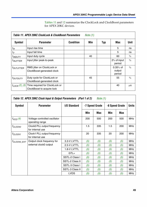
Tables 11 and 12 summarize the ClockLock and ClockBoost parameters for APEX 20KC devices.
Table 11. APEX 20KC ClockLock & ClockBoost Parameters Note (1)
Symbol Parameter Condition Min Typ Max Unit
tR Input rise time 5 ns
tF Input fall time 5 ns
t INDUTY Input duty cycle 40 60 %
t INJITTER Input jitter peak-to-peak 2% of input period
%
tOUTJITTER RMS jitter on ClockLock or ClockBoost-generated clock
0.35% of output period
%
tOUTDUTY Duty cycle for ClockLock or ClockBoost-generated clock
45 55 %
tLOCK (2), (3) Time required for ClockLock or ClockBoost to acquire lock
40 µs
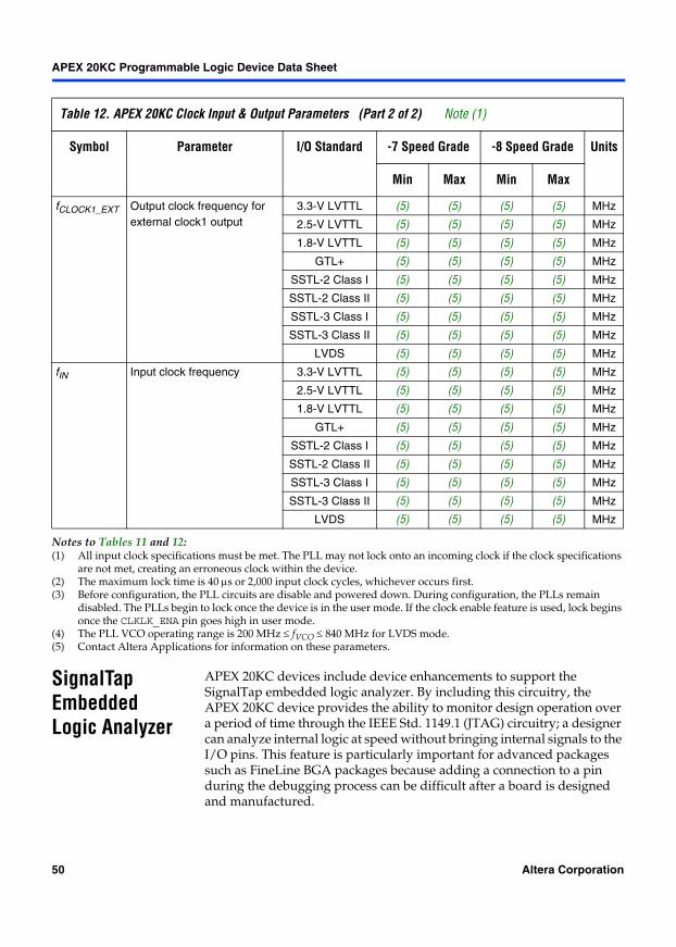
Table 12. APEX 20KC Clock Input & Output Parameters (Part 1 of 2) Note (1)
Symbol Parameter I/O Standard -7 Speed Grade -8 Speed Grade Units
Min Max Min Max
fVCO (4) Voltage controlled oscillator operating range
200 500 200 500 MHz
fCLOCK0 Clock0 PLL output frequency for internal use
1.5 335 1.5 200 MHz
fCLOCK1 Clock1 PLL output frequency for internal use
20 335 20 200 MHz
fCLOCK0_EXT Output clock frequency for external clock0 output
3.3-V LVTTL (5) (5) (5) (5) MHz
2.5-V LVTTL (5) (5) (5) (5) MHz
1.8-V LVTTL (5) (5) (5) (5) MHz
GTL+ (5) (5) (5) (5) MHz
SSTL-2 Class I (5) (5) (5) (5) MHz
SSTL-2 Class II (5) (5) (5) (5) MHz
SSTL-3 Class I (5) (5) (5) (5) MHz
SSTL-3 Class II (5) (5) (5) (5) MHz
LVDS (5) (5) (5) (5) MHz
Altera Corporation 49
APEX 20KC Programmable Logic Device Data Sheet
Notes to Tables 11 and 12:(1) All input clock specifications must be met. The PLL may not lock onto an incoming clock if the clock specifications
are not met, creating an erroneous clock within the device.(2) The maximum lock time is 40 µs or 2,000 input clock cycles, whichever occurs first.(3) Before configuration, the PLL circuits are disable and powered down. During configuration, the PLLs remain
disabled. The PLLs begin to lock once the device is in the user mode. If the clock enable feature is used, lock begins once the CLKLK_ENA pin goes high in user mode.
(4) The PLL VCO operating range is 200 MHz ≤ fVCO ≤ 840 MHz for LVDS mode.(5) Contact Altera Applications for information on these parameters.
SignalTap Embedded Logic Analyzer
APEX 20KC devices include device enhancements to support the SignalTap embedded logic analyzer. By including this circuitry, the APEX 20KC device provides the ability to monitor design operation over a period of time through the IEEE Std. 1149.1 (JTAG) circuitry; a designer can analyze internal logic at speed without bringing internal signals to the I/O pins. This feature is particularly important for advanced packages such as FineLine BGA packages because adding a connection to a pin during the debugging process can be difficult after a board is designed and manufactured.
fCLOCK1_EXT Output clock frequency for external clock1 output
3.3-V LVTTL (5) (5) (5) (5) MHz
2.5-V LVTTL (5) (5) (5) (5) MHz
1.8-V LVTTL (5) (5) (5) (5) MHz
GTL+ (5) (5) (5) (5) MHz
SSTL-2 Class I (5) (5) (5) (5) MHz
SSTL-2 Class II (5) (5) (5) (5) MHz
SSTL-3 Class I (5) (5) (5) (5) MHz
SSTL-3 Class II (5) (5) (5) (5) MHz
LVDS (5) (5) (5) (5) MHz
fIN Input clock frequency 3.3-V LVTTL (5) (5) (5) (5) MHz
2.5-V LVTTL (5) (5) (5) (5) MHz
1.8-V LVTTL (5) (5) (5) (5) MHz
GTL+ (5) (5) (5) (5) MHz
SSTL-2 Class I (5) (5) (5) (5) MHz
SSTL-2 Class II (5) (5) (5) (5) MHz
SSTL-3 Class I (5) (5) (5) (5) MHz
SSTL-3 Class II (5) (5) (5) (5) MHz
LVDS (5) (5) (5) (5) MHz
Table 12. APEX 20KC Clock Input & Output Parameters (Part 2 of 2) Note (1)
Symbol Parameter I/O Standard -7 Speed Grade -8 Speed Grade Units
Min Max Min Max
50 Altera Corporation
APEX 20KC Programmable Logic Device Data Sheet
IEEE Std. 1149.1 (JTAG) Boundary-Scan Support
All APEX 20KC devices provide JTAG BST circuitry that complies with the IEEE Std. 1149.1-1990 specification. JTAG boundary-scan testing can be performed before or after configuration, but not during configuration. APEX 20KC devices can also use the JTAG port for configuration with the Quartus II software or with hardware using either Jam Files (.jam) or Jam Byte-Code Files (.jbc). Finally, APEX 20KC devices use the JTAG port to monitor the logic operation of the device with the SignalTap embedded logic analyzer. APEX 20KC devices support the JTAG instructions shown in Table 13.
Table 13. APEX 20KC JTAG Instructions
JTAG Instruction Description
SAMPLE/PRELOAD Allows a snapshot of signals at the device pins to be captured and examined during normal device operation, and permits an initial data pattern to be output at the device pins. Also used by the SignalTap embedded logic analyzer.
EXTEST Allows the external circuitry and board-level interconnections to be tested by forcing a test pattern at the output pins and capturing test results at the input pins.
BYPASS Places the 1-bit bypass register between the TDI and TDO pins, which allows the BST data to pass synchronously through selected devices to adjacent devices during normal device operation.
USERCODE Selects the 32-bit USERCODE register and places it between the TDI and TDO pins, allowing the USERCODE to be serially shifted out of TDO.
IDCODE Selects the IDCODE register and places it between TDI and TDO, allowing the IDCODE to be serially shifted out of TDO.
ICR Instructions Used when configuring an APEX 20KC device via the JTAG port with a MasterBlasterTM or ByteBlasterMVTM download cable, or when using a Jam File or Jam Byte-Code File via an embedded processor.
SignalTap Instructions
Monitors internal device operation with the SignalTap embedded logic analyzer.
Altera Corporation 51
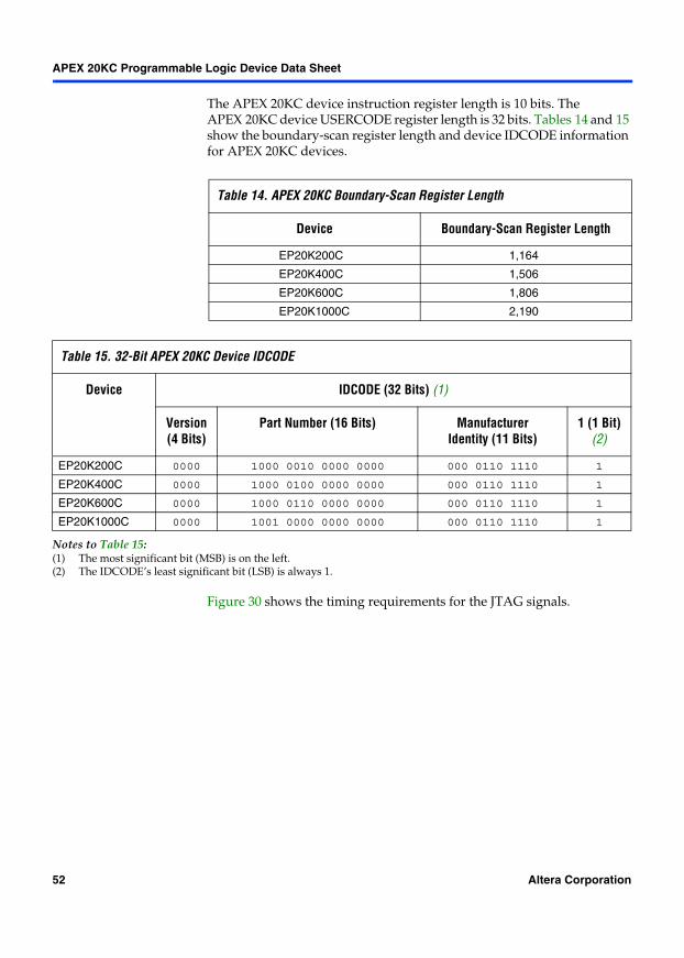
APEX 20KC Programmable Logic Device Data Sheet
The APEX 20KC device instruction register length is 10 bits. The APEX 20KC device USERCODE register length is 32 bits. Tables 14 and 15 show the boundary-scan register length and device IDCODE information for APEX 20KC devices.
Notes to Table 15:(1) The most significant bit (MSB) is on the left.(2) The IDCODE’s least significant bit (LSB) is always 1.
Figure 30 shows the timing requirements for the JTAG signals.
Table 14. APEX 20KC Boundary-Scan Register Length
Device Boundary-Scan Register Length
EP20K200C 1,164
EP20K400C 1,506
EP20K600C 1,806
EP20K1000C 2,190
Table 15. 32-Bit APEX 20KC Device IDCODE
Device IDCODE (32 Bits) (1)
Version (4 Bits)
Part Number (16 Bits) ManufacturerIdentity (11 Bits)
1 (1 Bit)(2)
EP20K200C 0000 1000 0010 0000 0000 000 0110 1110 1
EP20K400C 0000 1000 0100 0000 0000 000 0110 1110 1
EP20K600C 0000 1000 0110 0000 0000 000 0110 1110 1
EP20K1000C 0000 1001 0000 0000 0000 000 0110 1110 1
52 Altera Corporation
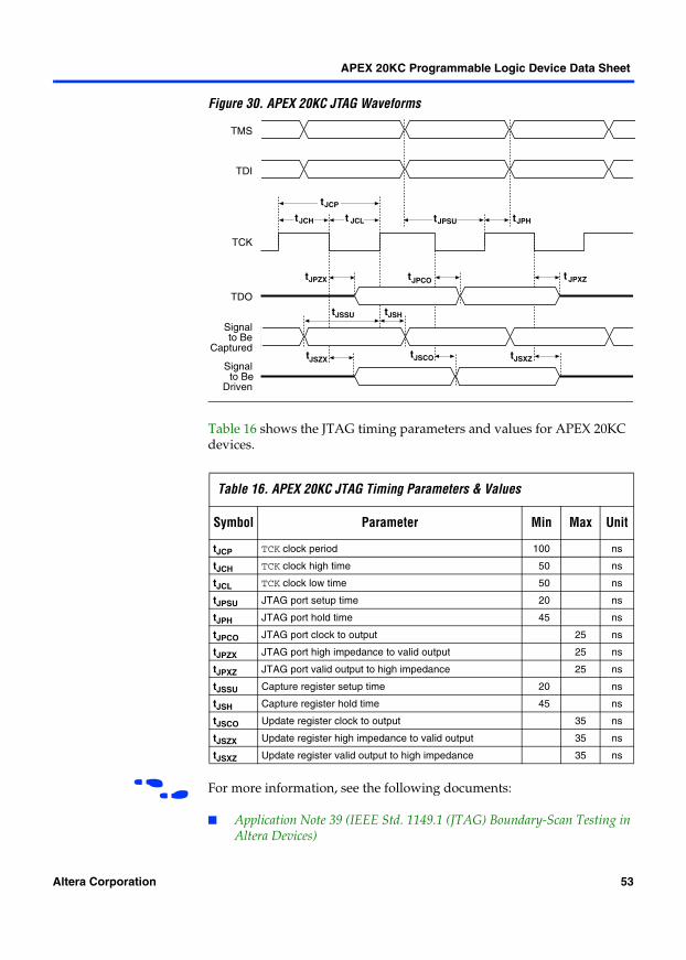
APEX 20KC Programmable Logic Device Data Sheet
Figure 30. APEX 20KC JTAG Waveforms
Table 16 shows the JTAG timing parameters and values for APEX 20KC devices.
f For more information, see the following documents:
Application Note 39 (IEEE Std. 1149.1 (JTAG) Boundary-Scan Testing in Altera Devices)
Table 16. APEX 20KC JTAG Timing Parameters & Values
Symbol Parameter Min Max Unit
tJCP TCK clock period 100 ns
tJCH TCK clock high time 50 ns
tJCL TCK clock low time 50 ns
tJPSU JTAG port setup time 20 ns
tJPH JTAG port hold time 45 ns
tJPCO JTAG port clock to output 25 ns
tJPZX JTAG port high impedance to valid output 25 ns
tJPXZ JTAG port valid output to high impedance 25 ns
tJSSU Capture register setup time 20 ns
tJSH Capture register hold time 45 ns
tJSCO Update register clock to output 35 ns
tJSZX Update register high impedance to valid output 35 ns
tJSXZ Update register valid output to high impedance 35 ns
TDO
TCK
tJPZX tJPCO
tJPH
t JPXZ
tJCP
tJPSU t JCL tJCH
TDI
TMS
Signalto Be
Captured
Signalto Be
Driven
tJSZX
tJSSU tJSH
tJSCO tJSXZ
Altera Corporation 53
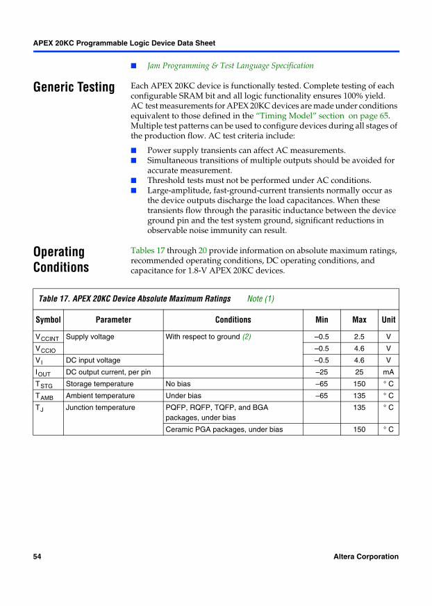
APEX 20KC Programmable Logic Device Data Sheet
Jam Programming & Test Language Specification
Generic Testing Each APEX 20KC device is functionally tested. Complete testing of each configurable SRAM bit and all logic functionality ensures 100% yield. AC test measurements for APEX 20KC devices are made under conditions equivalent to those defined in the “Timing Model” section on page 65. Multiple test patterns can be used to configure devices during all stages of the production flow. AC test criteria include:
Power supply transients can affect AC measurements. Simultaneous transitions of multiple outputs should be avoided for
accurate measurement. Threshold tests must not be performed under AC conditions. Large-amplitude, fast-ground-current transients normally occur as
the device outputs discharge the load capacitances. When these transients flow through the parasitic inductance between the device ground pin and the test system ground, significant reductions in observable noise immunity can result.
Operating Conditions
Tables 17 through 20 provide information on absolute maximum ratings, recommended operating conditions, DC operating conditions, and capacitance for 1.8-V APEX 20KC devices.
Table 17. APEX 20KC Device Absolute Maximum Ratings Note (1)
Symbol Parameter Conditions Min Max Unit
VCCINT Supply voltage With respect to ground (2) –0.5 2.5 V
VCCIO –0.5 4.6 V
VI DC input voltage –0.5 4.6 V
IOUT DC output current, per pin –25 25 mA
TSTG Storage temperature No bias –65 150 ° C
TAMB Ambient temperature Under bias –65 135 ° C
TJ Junction temperature PQFP, RQFP, TQFP, and BGA packages, under bias
135 ° C
Ceramic PGA packages, under bias 150 ° C
54 Altera Corporation
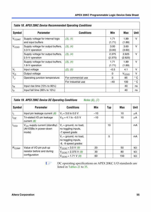
APEX 20KC Programmable Logic Device Data Sheet
1 DC operating specifications on APEX 20KC I/O standards are listed in Tables 21 to 35.
Table 18. APEX 20KC Device Recommended Operating Conditions
Symbol Parameter Conditions Min Max Unit
VCCINT Supply voltage for internal logic and input buffers
(3), (4) 1.71 (1.71)
1.89 (1.89)
V
VCCIO Supply voltage for output buffers, 3.3-V operation
(3), (4) 3.00 (3.00)
3.60 (3.60)
V
Supply voltage for output buffers, 2.5-V operation
(3), (4) 2.375 (2.375)
2.625 (2.625)
V
Supply voltage for output buffers, 1.8-V operation
(3), (4) 1.71 (1.71)
1.89 (1.89)
V
VI Input voltage (2), (5) –0.5 4.1 V
VO Output voltage 0 VCCIO V
TJ Operating junction temperature For commercial use 0 85 ° C
For industrial use –40 100 ° C
tR Input rise time (10% to 90%) 40 ns
tF Input fall time (90% to 10%) 40 ns
Table 19. APEX 20KC Device DC Operating Conditions Notes (6), (7)
Symbol Parameter Conditions Min Typ Max Unit
I I Input pin leakage current (8) VI = 3.6 to 0.0 V –10 10 µA
IOZ Tri-stated I/O pin leakage current (8)
VO = 4.1 to –0.5 V –10 10 µA
ICC0 VCC supply current (standby) (All ESBs in power-down mode)
VI = ground, no load, no toggling inputs, -7 speed grade
10 mA
VI = ground, no load, no toggling inputs,-8, -9 speed grades
5 mA
RCONF Value of I/O pin pull-up resistor before and during configuration
VCCIO = 3.0 V (9) 20 50 kΩ
VCCIO = 2.375 V (9) 30 80 kΩ
VCCIO = 1.71 V (9) 60 150 kΩ
Altera Corporation 55
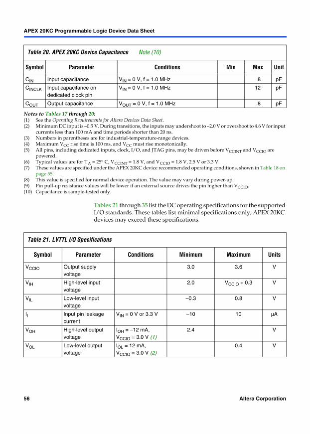
APEX 20KC Programmable Logic Device Data Sheet
Notes to Tables 17 through 20:(1) See the Operating Requirements for Altera Devices Data Sheet.(2) Minimum DC input is –0.5 V. During transitions, the inputs may undershoot to –2.0 V or overshoot to 4.6 V for input
currents less than 100 mA and time periods shorter than 20 ns.(3) Numbers in parentheses are for industrial-temperature-range devices.(4) Maximum VCC rise time is 100 ms, and VCC must rise monotonically.(5) All pins, including dedicated inputs, clock, I/O, and JTAG pins, may be driven before VCCINT and VCCIO are
powered.(6) Typical values are for TA = 25° C, VCCINT = 1.8 V, and VCCIO = 1.8 V, 2.5 V or 3.3 V.(7) These values are specified under the APEX 20KC device recommended operating conditions, shown in Table 18 on
page 55. (8) This value is specified for normal device operation. The value may vary during power-up.(9) Pin pull-up resistance values will be lower if an external source drives the pin higher than VCCIO.(10) Capacitance is sample-tested only.
Tables 21 through 35 list the DC operating specifications for the supported I/O standards. These tables list minimal specifications only; APEX 20KC devices may exceed these specifications.
Table 20. APEX 20KC Device Capacitance Note (10)
Symbol Parameter Conditions Min Max Unit
CIN Input capacitance VIN = 0 V, f = 1.0 MHz 8 pF
CINCLK Input capacitance on dedicated clock pin
VIN = 0 V, f = 1.0 MHz 12 pF
COUT Output capacitance VOUT = 0 V, f = 1.0 MHz 8 pF
Table 21. LVTTL I/O Specifications
Symbol Parameter Conditions Minimum Maximum Units
VCCIO Output supply voltage
3.0 3.6 V
VIH High-level input voltage
2.0 VCCIO + 0.3 V
VIL Low-level input voltage
–0.3 0.8 V
II Input pin leakage current
VIN = 0 V or 3.3 V –10 10 µA
VOH High-level output voltage
IOH = –12 mA, VCCIO = 3.0 V (1)
2.4 V
VOL Low-level output voltage
IOL = 12 mA, VCCIO = 3.0 V (2)
0.4 V
56 Altera Corporation
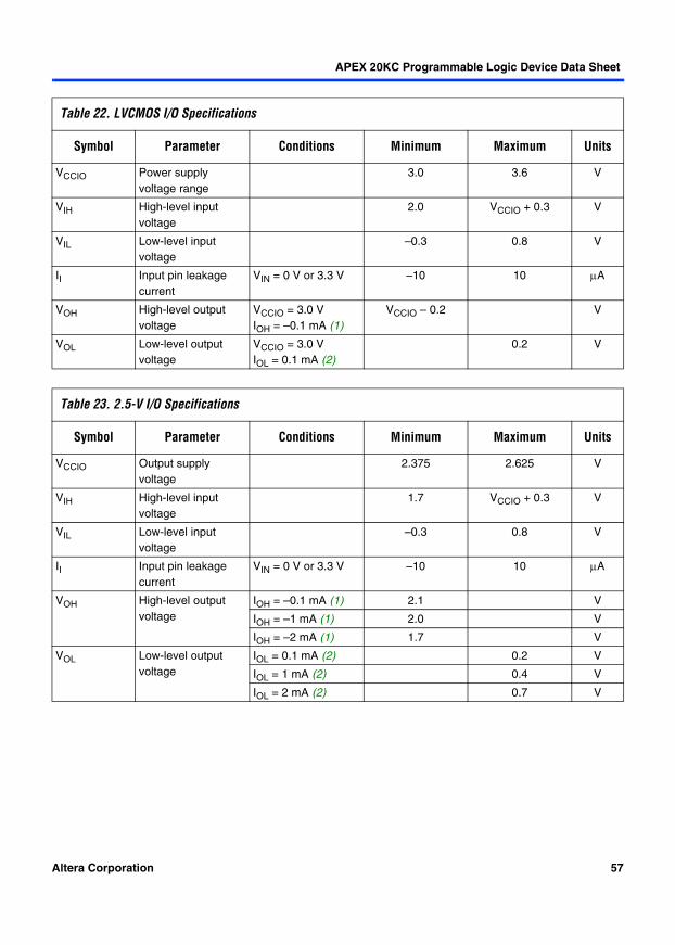
APEX 20KC Programmable Logic Device Data Sheet
Table 22. LVCMOS I/O Specifications
Symbol Parameter Conditions Minimum Maximum Units
VCCIO Power supply voltage range
3.0 3.6 V
VIH High-level input voltage
2.0 VCCIO + 0.3 V
VIL Low-level input voltage
–0.3 0.8 V
II Input pin leakage current
VIN = 0 V or 3.3 V –10 10 µA
VOH High-level output voltage
VCCIO = 3.0 V IOH = –0.1 mA (1)
VCCIO – 0.2 V
VOL Low-level output voltage
VCCIO = 3.0 VIOL = 0.1 mA (2)
0.2 V
Table 23. 2.5-V I/O Specifications
Symbol Parameter Conditions Minimum Maximum Units
VCCIO Output supply voltage
2.375 2.625 V
VIH High-level input voltage
1.7 VCCIO + 0.3 V
VIL Low-level input voltage
–0.3 0.8 V
II Input pin leakage current
VIN = 0 V or 3.3 V –10 10 µA
VOH High-level output voltage
IOH = –0.1 mA (1) 2.1 V
IOH = –1 mA (1) 2.0 V
IOH = –2 mA (1) 1.7 V
VOL Low-level output voltage
IOL = 0.1 mA (2) 0.2 V
IOL = 1 mA (2) 0.4 V
IOL = 2 mA (2) 0.7 V
Altera Corporation 57
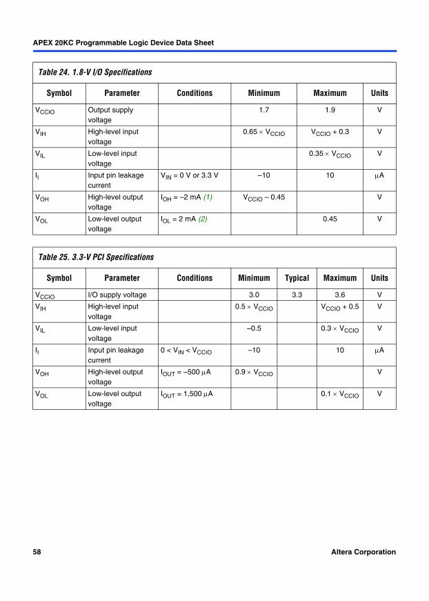
APEX 20KC Programmable Logic Device Data Sheet
Table 24. 1.8-V I/O Specifications
Symbol Parameter Conditions Minimum Maximum Units
VCCIO Output supply voltage
1.7 1.9 V
VIH High-level input voltage
0.65 × VCCIO VCCIO + 0.3 V
VIL Low-level input voltage
0.35 × VCCIO V
II Input pin leakage current
VIN = 0 V or 3.3 V –10 10 µA
VOH High-level output voltage
IOH = –2 mA (1) VCCIO – 0.45 V
VOL Low-level output voltage
IOL = 2 mA (2) 0.45 V
Table 25. 3.3-V PCI Specifications
Symbol Parameter Conditions Minimum Typical Maximum Units
VCCIO I/O supply voltage 3.0 3.3 3.6 V
VIH High-level input voltage
0.5 × VCCIO VCCIO + 0.5 V
VIL Low-level input voltage
–0.5 0.3 × VCCIO V
II Input pin leakage current
0 < VIN < VCCIO –10 10 µA
VOH High-level output voltage
IOUT = –500 µA 0.9 × VCCIO V
VOL Low-level output voltage
IOUT = 1,500 µA 0.1 × VCCIO V
58 Altera Corporation
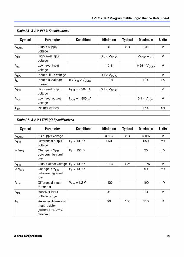
APEX 20KC Programmable Logic Device Data Sheet
Table 26. 3.3-V PCI-X Specifications
Symbol Parameter Conditions Minimum Typical Maximum Units
VCCIO Output supply voltage
3.0 3.3 3.6 V
VIH High-level input voltage
0.5 × VCCIO VCCIO + 0.5 V
VIL Low-level input voltage
–0.5 0.35 × VCCIO V
VIPU Input pull-up voltage 0.7 × VCCIO V
IIL Input pin leakage current
0 < VIN < VCCIO –10.0 10.0 µA
VOH High-level output voltage
IOUT = –500 µA 0.9 × VCCIO V
VOL Low-level output voltage
IOUT = 1,500 µA 0.1 × VCCIO V
Lpin Pin Inductance 15.0 nH
Table 27. 3.3-V LVDS I/O Specifications
Symbol Parameter Conditions Minimum Typical Maximum Units
VCCIO I/O supply voltage 3.135 3.3 3.465 V
VOD Differential output voltage
RL = 100 Ω 250 650 mV
∆ VOD Change in VOD between high and low
RL = 100 Ω 50 mV
VOS Output offset voltage RL = 100 Ω 1.125 1.25 1.375 V
∆ VOS Change in VOS between high and low
RL = 100 Ω 50 mV
VTH Differential input threshold
VCM = 1.2 V –100 100 mV
VIN Receiver input voltage range
0.0 2.4 V
RL Receiver differential input resistor (external to APEX devices)
90 100 110 Ω
Altera Corporation 59
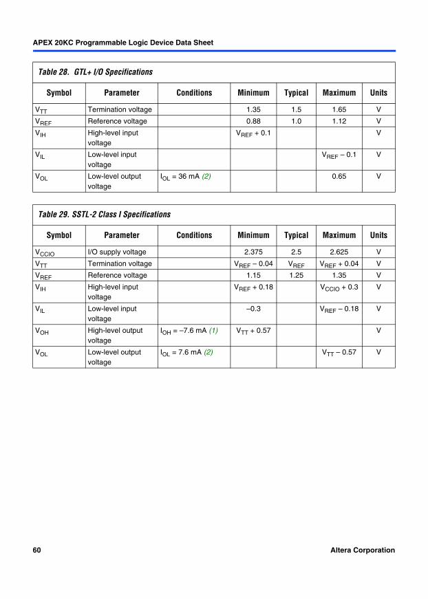
APEX 20KC Programmable Logic Device Data Sheet
Table 28. GTL+ I/O Specifications
Symbol Parameter Conditions Minimum Typical Maximum Units
VTT Termination voltage 1.35 1.5 1.65 V
VREF Reference voltage 0.88 1.0 1.12 V
VIH High-level input voltage
VREF + 0.1 V
VIL Low-level input voltage
VREF – 0.1 V
VOL Low-level output voltage
IOL = 36 mA (2) 0.65 V
Table 29. SSTL-2 Class I Specifications
Symbol Parameter Conditions Minimum Typical Maximum Units
VCCIO I/O supply voltage 2.375 2.5 2.625 V
VTT Termination voltage VREF – 0.04 VREF VREF + 0.04 V
VREF Reference voltage 1.15 1.25 1.35 V
VIH High-level input voltage
VREF + 0.18 VCCIO + 0.3 V
VIL Low-level input voltage
–0.3 VREF – 0.18 V
VOH High-level output voltage
IOH = –7.6 mA (1) VTT + 0.57 V
VOL Low-level output voltage
IOL = 7.6 mA (2) VTT – 0.57 V
60 Altera Corporation
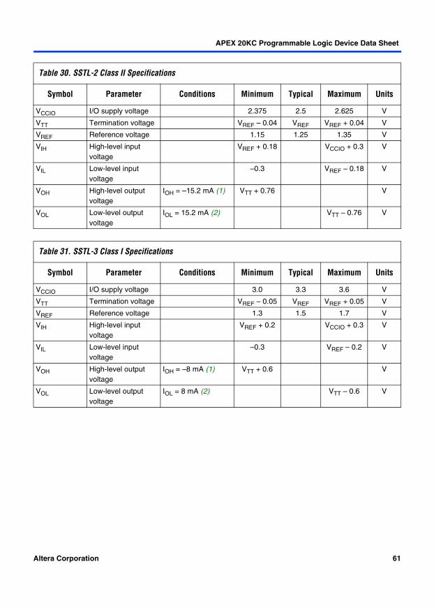
APEX 20KC Programmable Logic Device Data Sheet
Table 30. SSTL-2 Class II Specifications
Symbol Parameter Conditions Minimum Typical Maximum Units
VCCIO I/O supply voltage 2.375 2.5 2.625 V
VTT Termination voltage VREF – 0.04 VREF VREF + 0.04 V
VREF Reference voltage 1.15 1.25 1.35 V
VIH High-level input voltage
VREF + 0.18 VCCIO + 0.3 V
VIL Low-level input voltage
–0.3 VREF – 0.18 V
VOH High-level output voltage
IOH = –15.2 mA (1) VTT + 0.76 V
VOL Low-level output voltage
IOL = 15.2 mA (2) VTT – 0.76 V
Table 31. SSTL-3 Class I Specifications
Symbol Parameter Conditions Minimum Typical Maximum Units
VCCIO I/O supply voltage 3.0 3.3 3.6 V
VTT Termination voltage VREF – 0.05 VREF VREF + 0.05 V
VREF Reference voltage 1.3 1.5 1.7 V
VIH High-level input voltage
VREF + 0.2 VCCIO + 0.3 V
VIL Low-level input voltage
–0.3 VREF – 0.2 V
VOH High-level output voltage
IOH = –8 mA (1) VTT + 0.6 V
VOL Low-level output voltage
IOL = 8 mA (2) VTT – 0.6 V
Altera Corporation 61
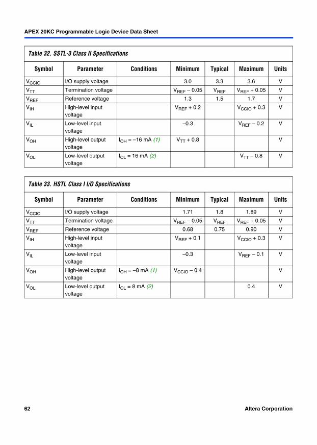
APEX 20KC Programmable Logic Device Data Sheet
Table 32. SSTL-3 Class II Specifications
Symbol Parameter Conditions Minimum Typical Maximum Units
VCCIO I/O supply voltage 3.0 3.3 3.6 V
VTT Termination voltage VREF – 0.05 VREF VREF + 0.05 V
VREF Reference voltage 1.3 1.5 1.7 V
VIH High-level input voltage
VREF + 0.2 VCCIO + 0.3 V
VIL Low-level input voltage
–0.3 VREF – 0.2 V
VOH High-level output voltage
IOH = –16 mA (1) VTT + 0.8 V
VOL Low-level output voltage
IOL = 16 mA (2) VTT – 0.8 V
Table 33. HSTL Class I I/O Specifications
Symbol Parameter Conditions Minimum Typical Maximum Units
VCCIO I/O supply voltage 1.71 1.8 1.89 V
VTT Termination voltage VREF – 0.05 VREF VREF + 0.05 V
VREF Reference voltage 0.68 0.75 0.90 V
VIH High-level input voltage
VREF + 0.1 VCCIO + 0.3 V
VIL Low-level input voltage
–0.3 VREF – 0.1 V
VOH High-level output voltage
IOH = –8 mA (1) VCCIO – 0.4 V
VOL Low-level output voltage
IOL = 8 mA (2) 0.4 V
62 Altera Corporation
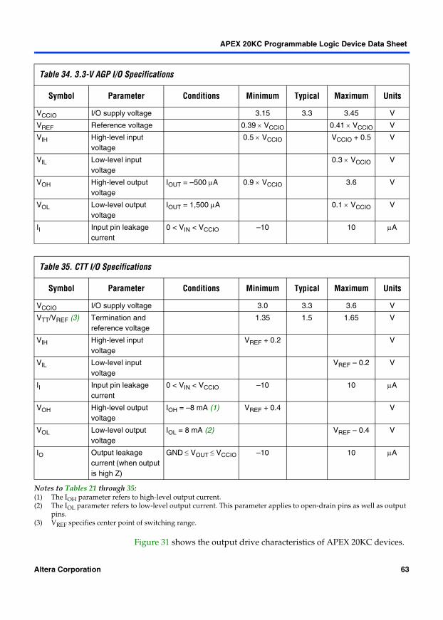
APEX 20KC Programmable Logic Device Data Sheet
Notes to Tables 21 through 35:(1) The IOH parameter refers to high-level output current.(2) The IOL parameter refers to low-level output current. This parameter applies to open-drain pins as well as output
pins.(3) VREF specifies center point of switching range.
Figure 31 shows the output drive characteristics of APEX 20KC devices.
Table 34. 3.3-V AGP I/O Specifications
Symbol Parameter Conditions Minimum Typical Maximum Units
VCCIO I/O supply voltage 3.15 3.3 3.45 V
VREF Reference voltage 0.39 × VCCIO 0.41 × VCCIO V
VIH High-level input voltage
0.5 × VCCIO VCCIO + 0.5 V
VIL Low-level input voltage
0.3 × VCCIO V
VOH High-level output voltage
IOUT = –500 µA 0.9 × VCCIO 3.6 V
VOL Low-level output voltage
IOUT = 1,500 µA 0.1 × VCCIO V
II Input pin leakage current
0 < VIN < VCCIO –10 10 µA
Table 35. CTT I/O Specifications
Symbol Parameter Conditions Minimum Typical Maximum Units
VCCIO I/O supply voltage 3.0 3.3 3.6 V
VTT/VREF (3) Termination and reference voltage
1.35 1.5 1.65 V
VIH High-level input voltage
VREF + 0.2 V
VIL Low-level input voltage
VREF – 0.2 V
II Input pin leakage current
0 < VIN < VCCIO –10 10 µA
VOH High-level output voltage
IOH = –8 mA (1) VREF + 0.4 V
VOL Low-level output voltage
IOL = 8 mA (2) VREF – 0.4 V
IO Output leakage current (when output is high Z)
GND ≤ VOUT ≤ VCCIO –10 10 µA
Altera Corporation 63
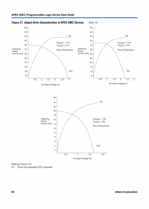
APEX 20KC Programmable Logic Device Data Sheet
Figure 31. Output Drive Characteristics of APEX 20KC Devices Note (1)
Note to Figure 31:(1) These are transient (AC) currents.
Vo Output Voltage (V)
IOL
IOH
2
4
6
8
10
12
14
16
18
20
22
24
26
Vo Output Voltage (V)
IOL
IOH
5
10
15
20
45
0.5 1 1.5 2 2.5 3
25
30
35
40
50
55
60
Typical IOOutputCurrent (mA)
10
20
30
40
50
60
70
80
90
0.5 1 1.5 2 2.5 3
Vo Output Voltage (V)
VCCINT = 1.8 VVCCIO = 3.3 V
Room Temperature
IOH
IOL
Typical IOOutputCurrent (mA)
100
110
120
0.5 1 1.5 2.0
VCCINT = 1.8 VVCCIO = 2.5V
Room Temperature
VCCINT = 1.8VVCCIO = 1.8V
Room Temperature
Typical IOOutputCurrent (mA)
64 Altera Corporation
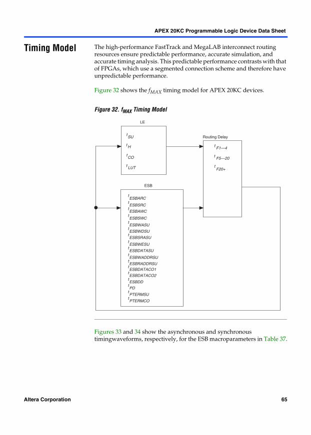
APEX 20KC Programmable Logic Device Data Sheet
Timing Model The high-performance FastTrack and MegaLAB interconnect routing resources ensure predictable performance, accurate simulation, and accurate timing analysis. This predictable performance contrasts with that of FPGAs, which use a segmented connection scheme and therefore have unpredictable performance.
Figure 32 shows the fMAX timing model for APEX 20KC devices.
Figure 32. fMAX Timing Model
Figures 33 and 34 show the asynchronous and synchronous timingwaveforms, respectively, for the ESB macroparameters in Table 37.
SU
H
CO
LUT
t
t
t
t
F1—4
F5—20
F20+
LE
ESB
Routing Delay
t
t
t
tESBARC
tESBSRC
tESBAWC
tESBSWC
tESBWASU
tESBWDSU
tESBSRASU
tESBWESU
tESBDATASU
tESBWADDRSU
tESBRADDRSU
tESBDATACO1
tESBDATACO2
tESBDD
tPD
tPTERMSU
tPTERMCO
Altera Corporation 65
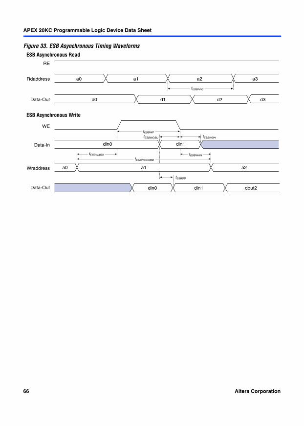
APEX 20KC Programmable Logic Device Data Sheet
Figure 33. ESB Asynchronous Timing Waveforms
ESB Asynchronous Write
ESB Asynchronous Read
RE
a0
d0 d3
tESBARC
a1 a2 a3
d2d1
Rdaddress
Data-Out
WE
a0
din1 dout2
tESBDD
a1 a2
din1
din0
tESBWCCOMB
tESBWASU tESBWAH
tESBWDH tESBWDSU
tESBWP
din0Data-In
Wraddress
Data-Out
66 Altera Corporation
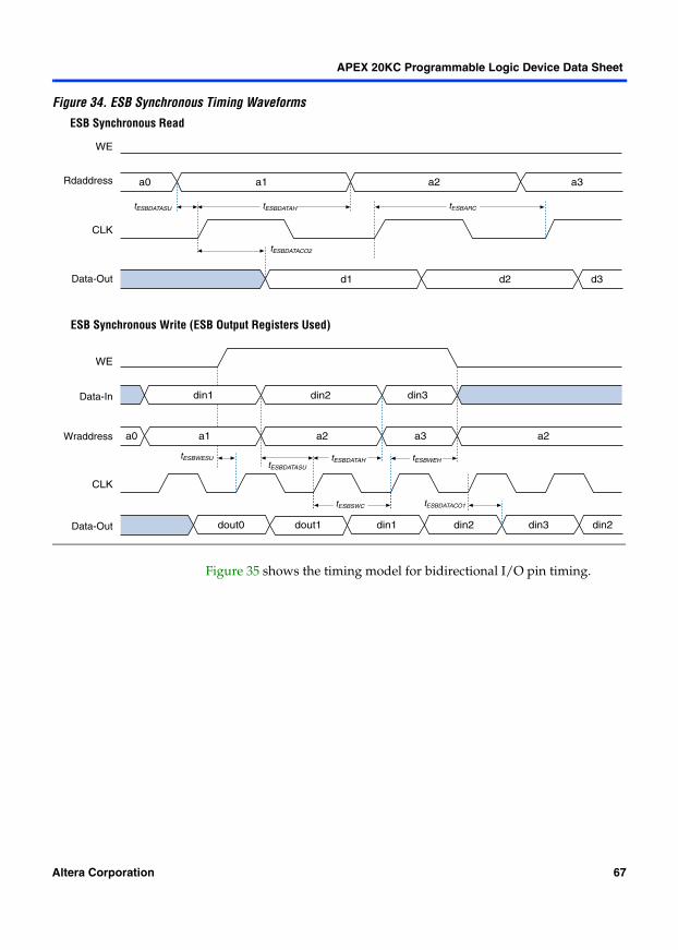
APEX 20KC Programmable Logic Device Data Sheet
Figure 34. ESB Synchronous Timing Waveforms
Figure 35 shows the timing model for bidirectional I/O pin timing.
WE
CLK
ESB Synchronous Read
a0
d3
tESBDATASU tESBARC
tESBDATACO2
a1 a2 a3
d2d1
tESBDATAH
a0
WE
CLK
dout0 din1 din2 din3 din2
tESBWESU
tESBSWC
tESBWEH
tESBDATACO1
a1 a2 a3 a2
din3din2din1
tESBDATAH tESBDATASU
ESB Synchronous Write (ESB Output Registers Used)
dout1
Rdaddress
Data-Out
Wraddress
Data-Out
Data-In
Altera Corporation 67
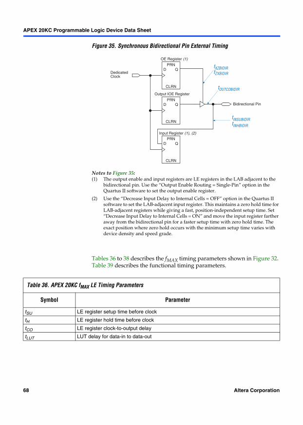
APEX 20KC Programmable Logic Device Data Sheet
Figure 35. Synchronous Bidirectional Pin External Timing
Notes to Figure 35:(1) The output enable and input registers are LE registers in the LAB adjacent to the
bidirectional pin. Use the “Output Enable Routing = Single-Pin” option in the Quartus II software to set the output enable register.
(2) Use the “Decrease Input Delay to Internal Cells = OFF” option in the Quartus II software to set the LAB-adjacent input register. This maintains a zero hold time for LAB-adjacent registers while giving a fast, position-independent setup time. Set “Decrease Input Delay to Internal Cells = ON” and move the input register farther away from the bidirectional pin for a faster setup time with zero hold time. The exact position where zero hold occurs with the minimum setup time varies with device density and speed grade.
Tables 36 to 38 describes the fMAX timing parameters shown in Figure 32. Table 39 describes the functional timing parameters.
PRN
CLRN
D Q
PRN
CLRN
D Q
OE Register (1)
Bidirectional Pin
DedicatedClock
PRN
CLRN
D Q
Input Register (1), (2)
XZBIDIRt ZXBIDIRt
OUTCOBIDIRt
INSUBIDIRtINHBIDIRt
Output IOE Register
Table 36. APEX 20KC fMAX LE Timing Parameters
Symbol Parameter
tSU LE register setup time before clock
tH LE register hold time before clock
tCO LE register clock-to-output delay
tLUT LUT delay for data-in to data-out
68 Altera Corporation
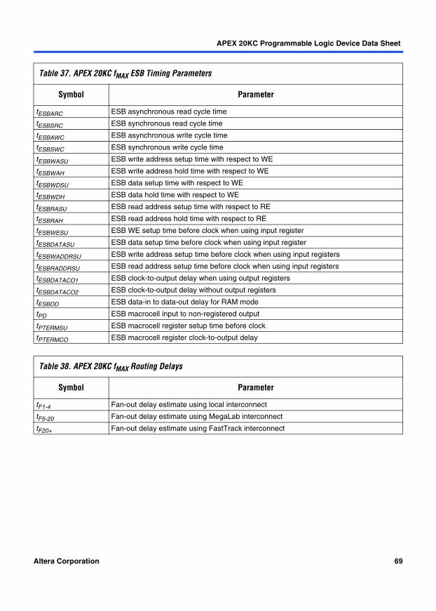
APEX 20KC Programmable Logic Device Data Sheet
Table 37. APEX 20KC fMAX ESB Timing Parameters
Symbol Parameter
tESBARC ESB asynchronous read cycle time
tESBSRC ESB synchronous read cycle time
tESBAWC ESB asynchronous write cycle time
tESBSWC ESB synchronous write cycle time
tESBWASU ESB write address setup time with respect to WE
tESBWAH ESB write address hold time with respect to WE
tESBWDSU ESB data setup time with respect to WE
tESBWDH ESB data hold time with respect to WE
tESBRASU ESB read address setup time with respect to RE
tESBRAH ESB read address hold time with respect to RE
tESBWESU ESB WE setup time before clock when using input register
tESBDATASU ESB data setup time before clock when using input register
tESBWADDRSU ESB write address setup time before clock when using input registers
tESBRADDRSU ESB read address setup time before clock when using input registers
tESBDATACO1 ESB clock-to-output delay when using output registers
tESBDATACO2 ESB clock-to-output delay without output registers
tESBDD ESB data-in to data-out delay for RAM mode
tPD ESB macrocell input to non-registered output
tPTERMSU ESB macrocell register setup time before clock
tPTERMCO ESB macrocell register clock-to-output delay
Table 38. APEX 20KC fMAX Routing Delays
Symbol Parameter
tF1-4 Fan-out delay estimate using local interconnect
tF5-20 Fan-out delay estimate using MegaLab interconnect
tF20+ Fan-out delay estimate using FastTrack interconnect
Altera Corporation 69
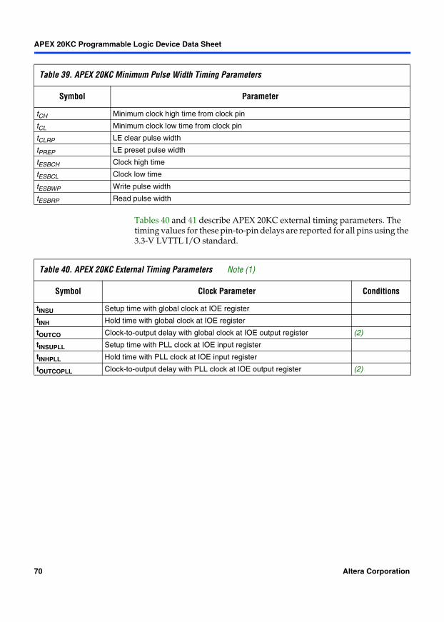
APEX 20KC Programmable Logic Device Data Sheet
Tables 40 and 41 describe APEX 20KC external timing parameters. The timing values for these pin-to-pin delays are reported for all pins using the 3.3-V LVTTL I/O standard.
Table 39. APEX 20KC Minimum Pulse Width Timing Parameters
Symbol Parameter
tCH Minimum clock high time from clock pin
tCL Minimum clock low time from clock pin
tCLRP LE clear pulse width
tPREP LE preset pulse width
tESBCH Clock high time
tESBCL Clock low time
tESBWP Write pulse width
tESBRP Read pulse width
Table 40. APEX 20KC External Timing Parameters Note (1)
Symbol Clock Parameter Conditions
tINSU Setup time with global clock at IOE register
tINH Hold time with global clock at IOE register
tOUTCO Clock-to-output delay with global clock at IOE output register (2)
tINSUPLL Setup time with PLL clock at IOE input register
tINHPLL Hold time with PLL clock at IOE input register
tOUTCOPLL Clock-to-output delay with PLL clock at IOE output register (2)
70 Altera Corporation
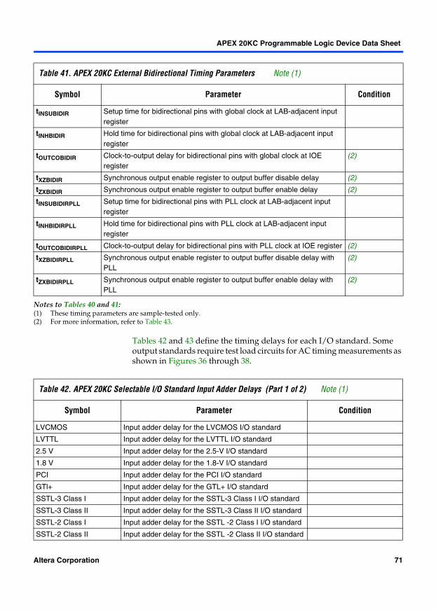
APEX 20KC Programmable Logic Device Data Sheet
Notes to Tables 40 and 41:(1) These timing parameters are sample-tested only.(2) For more information, refer to Table 43.
Tables 42 and 43 define the timing delays for each I/O standard. Some output standards require test load circuits for AC timing measurements as shown in Figures 36 through 38.
Table 41. APEX 20KC External Bidirectional Timing Parameters Note (1)
Symbol Parameter Condition
tINSUBIDIR Setup time for bidirectional pins with global clock at LAB-adjacent input register
tINHBIDIR Hold time for bidirectional pins with global clock at LAB-adjacent input register
tOUTCOBIDIR Clock-to-output delay for bidirectional pins with global clock at IOE register
(2)
tXZBIDIR Synchronous output enable register to output buffer disable delay (2)
tZXBIDIR Synchronous output enable register to output buffer enable delay (2)
tINSUBIDIRPLL Setup time for bidirectional pins with PLL clock at LAB-adjacent input register
tINHBIDIRPLL Hold time for bidirectional pins with PLL clock at LAB-adjacent input register
tOUTCOBIDIRPLL Clock-to-output delay for bidirectional pins with PLL clock at IOE register (2)
tXZBIDIRPLL Synchronous output enable register to output buffer disable delay with PLL
(2)
tZXBIDIRPLL Synchronous output enable register to output buffer enable delay with PLL
(2)
Table 42. APEX 20KC Selectable I/O Standard Input Adder Delays (Part 1 of 2) Note (1)
Symbol Parameter Condition
LVCMOS Input adder delay for the LVCMOS I/O standard
LVTTL Input adder delay for the LVTTL I/O standard
2.5 V Input adder delay for the 2.5-V I/O standard
1.8 V Input adder delay for the 1.8-V I/O standard
PCI Input adder delay for the PCI I/O standard
GTl+ Input adder delay for the GTL+ I/O standard
SSTL-3 Class I Input adder delay for the SSTL-3 Class I I/O standard
SSTL-3 Class II Input adder delay for the SSTL-3 Class II I/O standard
SSTL-2 Class I Input adder delay for the SSTL -2 Class I I/O standard
SSTL-2 Class II Input adder delay for the SSTL -2 Class II I/O standard
Altera Corporation 71
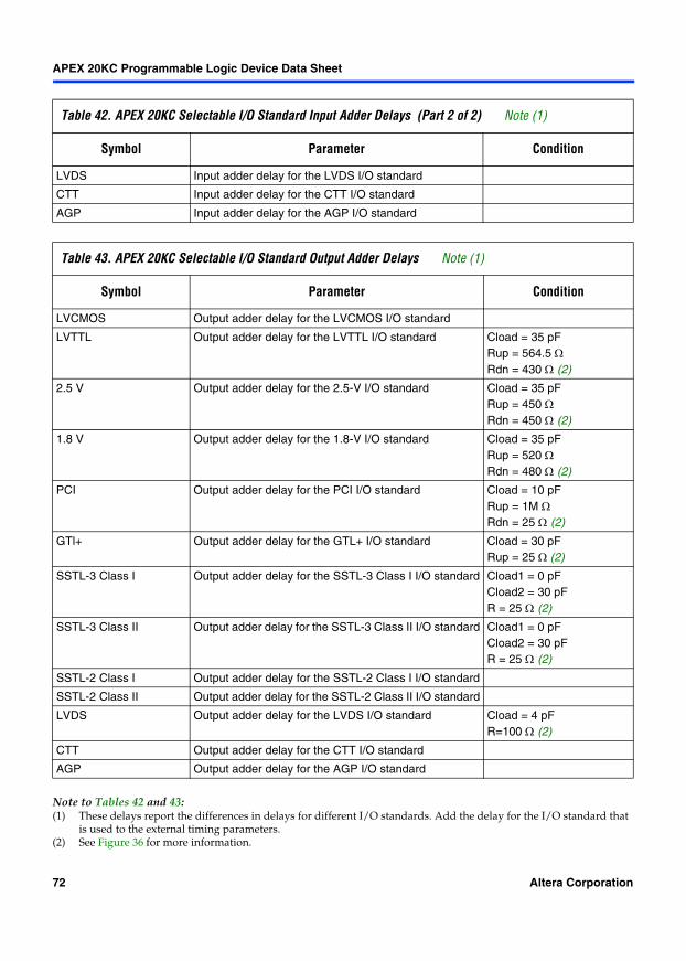
APEX 20KC Programmable Logic Device Data Sheet
Note to Tables 42 and 43:(1) These delays report the differences in delays for different I/O standards. Add the delay for the I/O standard that
is used to the external timing parameters.(2) See Figure 36 for more information.
LVDS Input adder delay for the LVDS I/O standard
CTT Input adder delay for the CTT I/O standard
AGP Input adder delay for the AGP I/O standard
Table 43. APEX 20KC Selectable I/O Standard Output Adder Delays Note (1)
Symbol Parameter Condition
LVCMOS Output adder delay for the LVCMOS I/O standard
LVTTL Output adder delay for the LVTTL I/O standard Cload = 35 pF Rup = 564.5 Ω Rdn = 430 Ω (2)
2.5 V Output adder delay for the 2.5-V I/O standard Cload = 35 pFRup = 450 ΩRdn = 450 Ω (2)
1.8 V Output adder delay for the 1.8-V I/O standard Cload = 35 pFRup = 520 ΩRdn = 480 Ω (2)
PCI Output adder delay for the PCI I/O standard Cload = 10 pFRup = 1M ΩRdn = 25 Ω (2)
GTl+ Output adder delay for the GTL+ I/O standard Cload = 30 pFRup = 25 Ω (2)
SSTL-3 Class I Output adder delay for the SSTL-3 Class I I/O standard Cload1 = 0 pF Cload2 = 30 pF R = 25 Ω (2)
SSTL-3 Class II Output adder delay for the SSTL-3 Class II I/O standard Cload1 = 0 pFCload2 = 30 pF R = 25 Ω (2)
SSTL-2 Class I Output adder delay for the SSTL-2 Class I I/O standard
SSTL-2 Class II Output adder delay for the SSTL-2 Class II I/O standard
LVDS Output adder delay for the LVDS I/O standard Cload = 4 pFR=100 Ω (2)
CTT Output adder delay for the CTT I/O standard
AGP Output adder delay for the AGP I/O standard
Table 42. APEX 20KC Selectable I/O Standard Input Adder Delays (Part 2 of 2) Note (1)
Symbol Parameter Condition
72 Altera Corporation
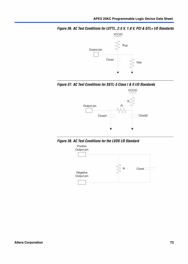
APEX 20KC Programmable Logic Device Data Sheet
Figure 36. AC Test Conditions for LVTTL, 2.5 V, 1.8 V, PCI & GTL+ I/O Standards
Figure 37. AC Test Conditions for SSTL-3 Class I & II I/O Standards
Figure 38. AC Test Conditions for the LVDS I/O Standard
Rup
Ouptut pin
CloadRdn
VCCIO
R
Output pin
Cload1 Cload2
R
VCCIO
R
PositiveOutput pin
CloadNegative
Output pin
Altera Corporation 73
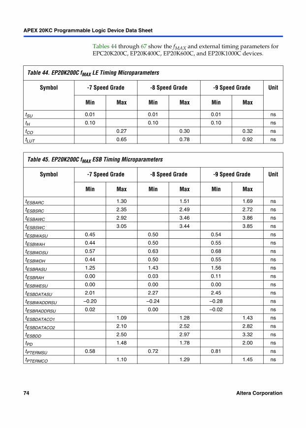
APEX 20KC Programmable Logic Device Data Sheet
Tables 44 through 67 show the fMAX and external timing parameters for EPC20K200C, EP20K400C, EP20K600C, and EP20K1000C devices.
Table 44. EP20K200C fMAX LE Timing Microparameters
Symbol -7 Speed Grade -8 Speed Grade -9 Speed Grade Unit
Min Max Min Max Min Max
tSU 0.01 0.01 0.01 ns
tH 0.10 0.10 0.10 ns
tCO 0.27 0.30 0.32 ns
tLUT 0.65 0.78 0.92 ns
Table 45. EP20K200C fMAX ESB Timing Microparameters
Symbol -7 Speed Grade -8 Speed Grade -9 Speed Grade Unit
Min Max Min Max Min Max
tESBARC 1.30 1.51 1.69 ns
tESBSRC 2.35 2.49 2.72 ns
tESBAWC 2.92 3.46 3.86 ns
tESBSWC 3.05 3.44 3.85 ns
tESBWASU 0.45 0.50 0.54 ns
tESBWAH 0.44 0.50 0.55 ns
tESBWDSU 0.57 0.63 0.68 ns
tESBWDH 0.44 0.50 0.55 ns
tESBRASU 1.25 1.43 1.56 ns
tESBRAH 0.00 0.03 0.11 ns
tESBWESU 0.00 0.00 0.00 ns
tESBDATASU 2.01 2.27 2.45 ns
tESBWADDRSU –0.20 –0.24 –0.28 ns
tESBRADDRSU 0.02 0.00 –0.02 ns
tESBDATACO1 1.09 1.28 1.43 ns
tESBDATACO2 2.10 2.52 2.82 ns
tESBDD 2.50 2.97 3.32 ns
tPD 1.48 1.78 2.00 ns
tPTERMSU 0.58 0.72 0.81 ns
tPTERMCO 1.10 1.29 1.45 ns
74 Altera Corporation
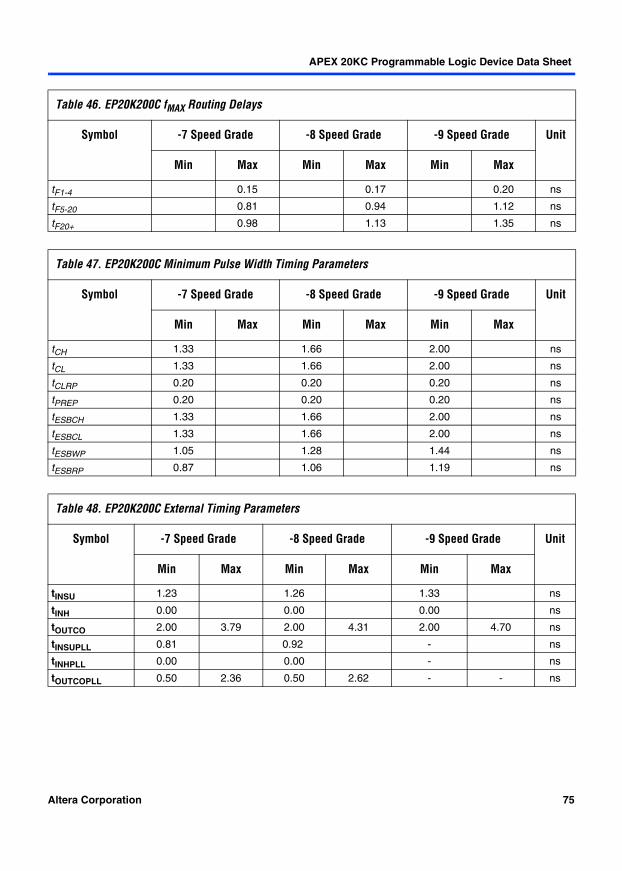
APEX 20KC Programmable Logic Device Data Sheet
Table 46. EP20K200C fMAX Routing Delays
Symbol -7 Speed Grade -8 Speed Grade -9 Speed Grade Unit
Min Max Min Max Min Max
tF1-4 0.15 0.17 0.20 ns
tF5-20 0.81 0.94 1.12 ns
tF20+ 0.98 1.13 1.35 ns
Table 47. EP20K200C Minimum Pulse Width Timing Parameters
Symbol -7 Speed Grade -8 Speed Grade -9 Speed Grade Unit
Min Max Min Max Min Max
tCH 1.33 1.66 2.00 ns
tCL 1.33 1.66 2.00 ns
tCLRP 0.20 0.20 0.20 ns
tPREP 0.20 0.20 0.20 ns
tESBCH 1.33 1.66 2.00 ns
tESBCL 1.33 1.66 2.00 ns
tESBWP 1.05 1.28 1.44 ns
tESBRP 0.87 1.06 1.19 ns
Table 48. EP20K200C External Timing Parameters
Symbol -7 Speed Grade -8 Speed Grade -9 Speed Grade Unit
Min Max Min Max Min Max
tINSU 1.23 1.26 1.33 ns
tINH 0.00 0.00 0.00 ns
tOUTCO 2.00 3.79 2.00 4.31 2.00 4.70 ns
tINSUPLL 0.81 0.92 - ns
tINHPLL 0.00 0.00 - ns
tOUTCOPLL 0.50 2.36 0.50 2.62 - - ns
Altera Corporation 75
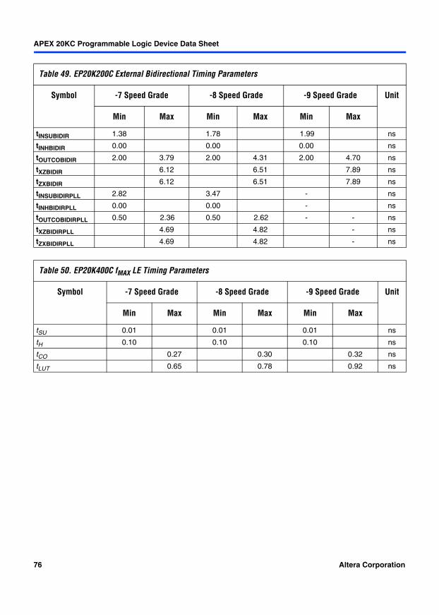
APEX 20KC Programmable Logic Device Data Sheet
Table 49. EP20K200C External Bidirectional Timing Parameters
Symbol -7 Speed Grade -8 Speed Grade -9 Speed Grade Unit
Min Max Min Max Min Max
tINSUBIDIR 1.38 1.78 1.99 ns
tINHBIDIR 0.00 0.00 0.00 ns
tOUTCOBIDIR 2.00 3.79 2.00 4.31 2.00 4.70 ns
tXZBIDIR 6.12 6.51 7.89 ns
tZXBIDIR 6.12 6.51 7.89 ns
tINSUBIDIRPLL 2.82 3.47 - ns
tINHBIDIRPLL 0.00 0.00 - ns
tOUTCOBIDIRPLL 0.50 2.36 0.50 2.62 - - ns
tXZBIDIRPLL 4.69 4.82 - ns
tZXBIDIRPLL 4.69 4.82 - ns
Table 50. EP20K400C fMAX LE Timing Parameters
Symbol -7 Speed Grade -8 Speed Grade -9 Speed Grade Unit
Min Max Min Max Min Max
tSU 0.01 0.01 0.01 ns
tH 0.10 0.10 0.10 ns
tCO 0.27 0.30 0.32 ns
tLUT 0.65 0.78 0.92 ns
76 Altera Corporation
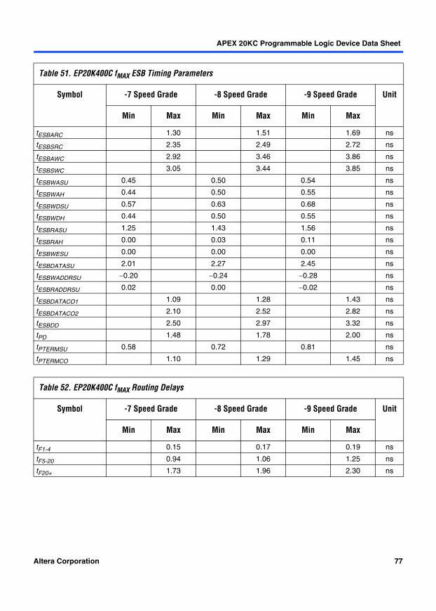
APEX 20KC Programmable Logic Device Data Sheet
Table 51. EP20K400C fMAX ESB Timing Parameters
Symbol -7 Speed Grade -8 Speed Grade -9 Speed Grade Unit
Min Max Min Max Min Max
tESBARC 1.30 1.51 1.69 ns
tESBSRC 2.35 2.49 2.72 ns
tESBAWC 2.92 3.46 3.86 ns
tESBSWC 3.05 3.44 3.85 ns
tESBWASU 0.45 0.50 0.54 ns
tESBWAH 0.44 0.50 0.55 ns
tESBWDSU 0.57 0.63 0.68 ns
tESBWDH 0.44 0.50 0.55 ns
tESBRASU 1.25 1.43 1.56 ns
tESBRAH 0.00 0.03 0.11 ns
tESBWESU 0.00 0.00 0.00 ns
tESBDATASU 2.01 2.27 2.45 ns
tESBWADDRSU −0.20 −0.24 −0.28 ns
tESBRADDRSU 0.02 0.00 −0.02 ns
tESBDATACO1 1.09 1.28 1.43 ns
tESBDATACO2 2.10 2.52 2.82 ns
tESBDD 2.50 2.97 3.32 ns
tPD 1.48 1.78 2.00 ns
tPTERMSU 0.58 0.72 0.81 ns
tPTERMCO 1.10 1.29 1.45 ns
Table 52. EP20K400C fMAX Routing Delays
Symbol -7 Speed Grade -8 Speed Grade -9 Speed Grade Unit
Min Max Min Max Min Max
tF1-4 0.15 0.17 0.19 ns
tF5-20 0.94 1.06 1.25 ns
tF20+ 1.73 1.96 2.30 ns
Altera Corporation 77

APEX 20KC Programmable Logic Device Data Sheet
Table 53. EP20K400C Minimum Pulse Width Timing Parameters
Symbol -7 Speed Grade -8 Speed Grade -9 Speed Grade Unit
Min Max Min Max Min Max
tCH 1.33 1.66 2.00 ns
tCL 1.33 1.66 2.00 ns
tCLRP 0.20 0.20 0.20 ns
tPREP 0.20 0.20 0.20 ns
tESBCH 1.33 1.66 2.00 ns
tESBCL 1.33 1.66 2.00 ns
tESBWP 1.05 1.28 1.44 ns
tESBRP 0.87 1.06 1.19 ns
Table 54. EP20K400C External Timing Parameters
Symbol -7 Speed Grade -8 Speed Grade -9 Speed Grade Unit
Min Max Min Max Min Max
tINSU 1.37 1.52 1.64 ns
tINH 0.00 0.00 0.00 ns
tOUTCO 2.00 4.25 2.00 4.61 2.00 5.03 ns
tINSUPLL 0.80 0.91 - ns
tINHPLL 0.00 0.00 - ns
tOUTCOPLL 0.50 2.27 0.50 2.55 - - ns
78 Altera Corporation
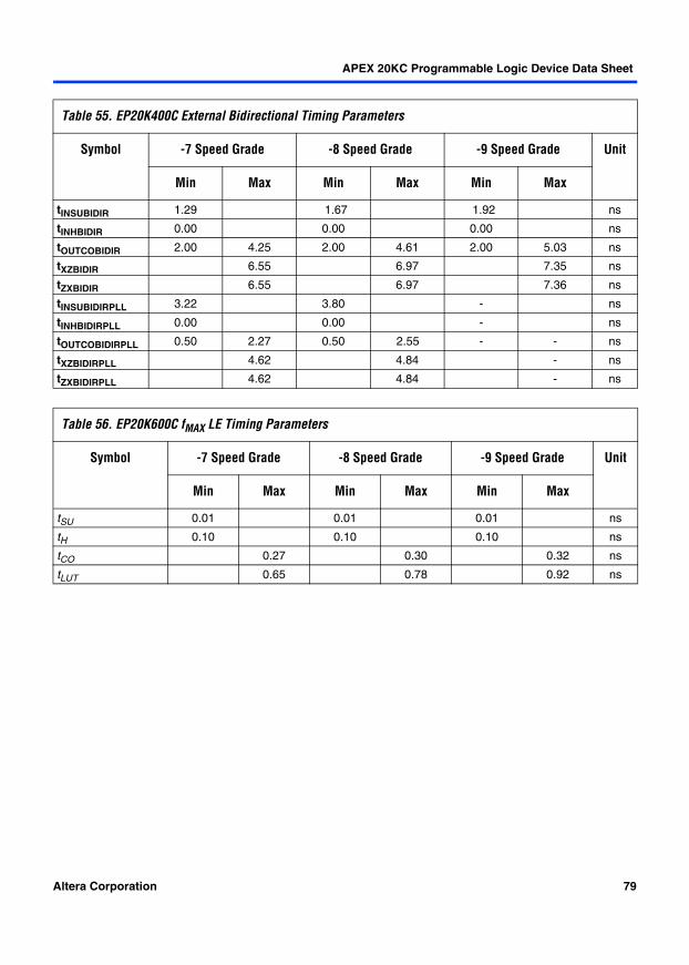
APEX 20KC Programmable Logic Device Data Sheet
Table 55. EP20K400C External Bidirectional Timing Parameters
Symbol -7 Speed Grade -8 Speed Grade -9 Speed Grade Unit
Min Max Min Max Min Max
tINSUBIDIR 1.29 1.67 1.92 ns
tINHBIDIR 0.00 0.00 0.00 ns
tOUTCOBIDIR 2.00 4.25 2.00 4.61 2.00 5.03 ns
tXZBIDIR 6.55 6.97 7.35 ns
tZXBIDIR 6.55 6.97 7.36 ns
tINSUBIDIRPLL 3.22 3.80 - ns
tINHBIDIRPLL 0.00 0.00 - ns
tOUTCOBIDIRPLL 0.50 2.27 0.50 2.55 - - ns
tXZBIDIRPLL 4.62 4.84 - ns
tZXBIDIRPLL 4.62 4.84 - ns
Table 56. EP20K600C fMAX LE Timing Parameters
Symbol -7 Speed Grade -8 Speed Grade -9 Speed Grade Unit
Min Max Min Max Min Max
tSU 0.01 0.01 0.01 ns
tH 0.10 0.10 0.10 ns
tCO 0.27 0.30 0.32 ns
tLUT 0.65 0.78 0.92 ns
Altera Corporation 79
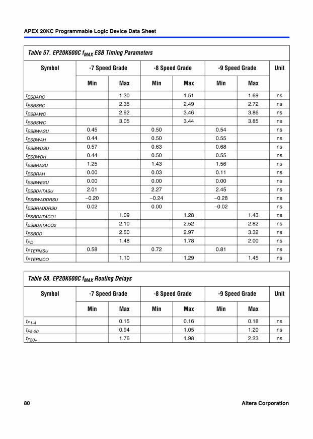
APEX 20KC Programmable Logic Device Data Sheet
Table 57. EP20K600C fMAX ESB Timing Parameters
Symbol -7 Speed Grade -8 Speed Grade -9 Speed Grade Unit
Min Max Min Max Min Max
tESBARC 1.30 1.51 1.69 ns
tESBSRC 2.35 2.49 2.72 ns
tESBAWC 2.92 3.46 3.86 ns
tESBSWC 3.05 3.44 3.85 ns
tESBWASU 0.45 0.50 0.54 ns
tESBWAH 0.44 0.50 0.55 ns
tESBWDSU 0.57 0.63 0.68 ns
tESBWDH 0.44 0.50 0.55 ns
tESBRASU 1.25 1.43 1.56 ns
tESBRAH 0.00 0.03 0.11 ns
tESBWESU 0.00 0.00 0.00 ns
tESBDATASU 2.01 2.27 2.45 ns
tESBWADDRSU −0.20 −0.24 −0.28 ns
tESBRADDRSU 0.02 0.00 −0.02 ns
tESBDATACO1 1.09 1.28 1.43 ns
tESBDATACO2 2.10 2.52 2.82 ns
tESBDD 2.50 2.97 3.32 ns
tPD 1.48 1.78 2.00 ns
tPTERMSU 0.58 0.72 0.81 ns
tPTERMCO 1.10 1.29 1.45 ns
Table 58. EP20K600C fMAX Routing Delays
Symbol -7 Speed Grade -8 Speed Grade -9 Speed Grade Unit
Min Max Min Max Min Max
tF1-4 0.15 0.16 0.18 ns
tF5-20 0.94 1.05 1.20 ns
tF20+ 1.76 1.98 2.23 ns
80 Altera Corporation
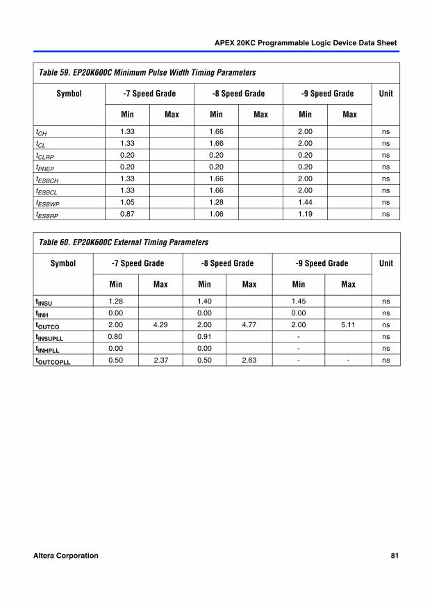
APEX 20KC Programmable Logic Device Data Sheet
Table 59. EP20K600C Minimum Pulse Width Timing Parameters
Symbol -7 Speed Grade -8 Speed Grade -9 Speed Grade Unit
Min Max Min Max Min Max
tCH 1.33 1.66 2.00 ns
tCL 1.33 1.66 2.00 ns
tCLRP 0.20 0.20 0.20 ns
tPREP 0.20 0.20 0.20 ns
tESBCH 1.33 1.66 2.00 ns
tESBCL 1.33 1.66 2.00 ns
tESBWP 1.05 1.28 1.44 ns
tESBRP 0.87 1.06 1.19 ns
Table 60. EP20K600C External Timing Parameters
Symbol -7 Speed Grade -8 Speed Grade -9 Speed Grade Unit
Min Max Min Max Min Max
tINSU 1.28 1.40 1.45 ns
tINH 0.00 0.00 0.00 ns
tOUTCO 2.00 4.29 2.00 4.77 2.00 5.11 ns
tINSUPLL 0.80 0.91 - ns
tINHPLL 0.00 0.00 - ns
tOUTCOPLL 0.50 2.37 0.50 2.63 - - ns
Altera Corporation 81

APEX 20KC Programmable Logic Device Data Sheet
Table 61. EP20K600C External Bidirectional Timing Parameters
Symbol -7 Speed Grade -8 Speed Grade -9 Speed Grade Unit
Min Max Min Max Min Max
tINSUBIDIR 2.03 2.57 2.97 ns
tINHBIDIR 0.00 0.00 0.00 ns
tOUTCOBIDIR 2.00 4.29 2.00 4.77 2.00 5.11 ns
tXZBIDIR 8.31 9.14 9.76 ns
tZXBIDIR 8.31 9.14 9.76 ns
tINSUBIDIRPLL 3.99 4.77 - ns
tINHBIDIRPLL 0.00 0.00 - ns
tOUTCOBIDIRPLL 0.50 2.37 0.50 2.63 - - ns
tXZBIDIRPLL 6.35 6.94 - ns
tZXBIDIRPLL 6.35 6.94 - ns
Table 62. EP20K1000C fMAX LE Timing Microparameters
Symbol -7 Speed Grade -8 Speed Grade -9 Speed Grade Unit
Min Max Min Max Min Max
tSU 0.01 0.01 0.01 ns
tH 0.10 0.10 0.10 ns
tCO 0.27 0.30 0.32 ns
tLUT 0.66 0.79 0.92 ns
82 Altera Corporation
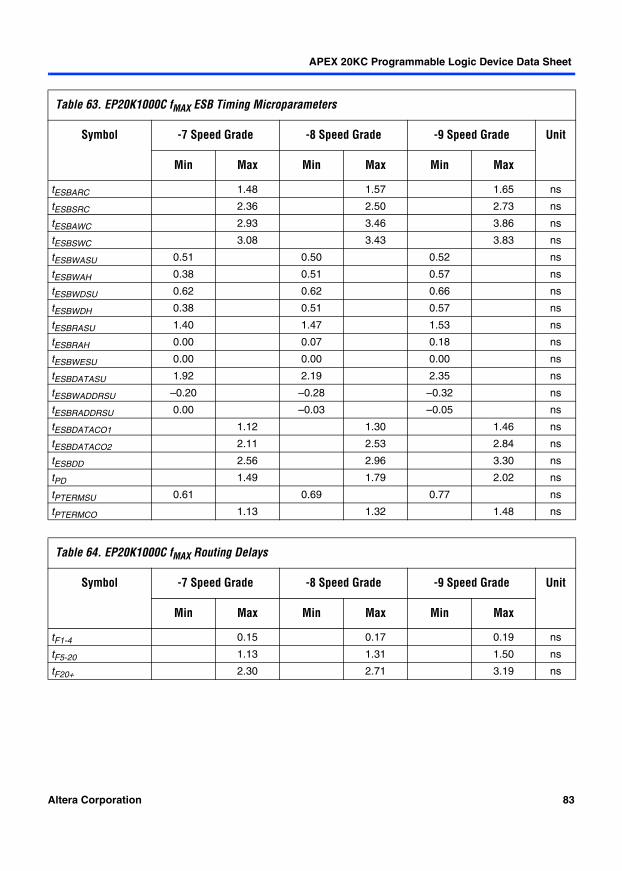
APEX 20KC Programmable Logic Device Data Sheet
Table 63. EP20K1000C fMAX ESB Timing Microparameters
Symbol -7 Speed Grade -8 Speed Grade -9 Speed Grade Unit
Min Max Min Max Min Max
tESBARC 1.48 1.57 1.65 ns
tESBSRC 2.36 2.50 2.73 ns
tESBAWC 2.93 3.46 3.86 ns
tESBSWC 3.08 3.43 3.83 ns
tESBWASU 0.51 0.50 0.52 ns
tESBWAH 0.38 0.51 0.57 ns
tESBWDSU 0.62 0.62 0.66 ns
tESBWDH 0.38 0.51 0.57 ns
tESBRASU 1.40 1.47 1.53 ns
tESBRAH 0.00 0.07 0.18 ns
tESBWESU 0.00 0.00 0.00 ns
tESBDATASU 1.92 2.19 2.35 ns
tESBWADDRSU –0.20 –0.28 –0.32 ns
tESBRADDRSU 0.00 –0.03 –0.05 ns
tESBDATACO1 1.12 1.30 1.46 ns
tESBDATACO2 2.11 2.53 2.84 ns
tESBDD 2.56 2.96 3.30 ns
tPD 1.49 1.79 2.02 ns
tPTERMSU 0.61 0.69 0.77 ns
tPTERMCO 1.13 1.32 1.48 ns
Table 64. EP20K1000C fMAX Routing Delays
Symbol -7 Speed Grade -8 Speed Grade -9 Speed Grade Unit
Min Max Min Max Min Max
tF1-4 0.15 0.17 0.19 ns
tF5-20 1.13 1.31 1.50 ns
tF20+ 2.30 2.71 3.19 ns
Altera Corporation 83
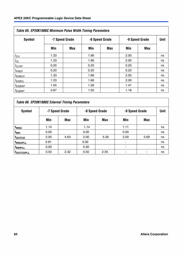
APEX 20KC Programmable Logic Device Data Sheet
Table 65. EP20K1000C Minimum Pulse Width Timing Parameters
Symbol -7 Speed Grade -8 Speed Grade -9 Speed Grade Unit
Min Max Min Max Min Max
tCH 1.33 1.66 2.00 ns
tCL 1.33 1.66 2.00 ns
tCLRP 0.20 0.20 0.20 ns
tPREP 0.20 0.20 0.20 ns
tESBCH 1.33 1.66 2.00 ns
tESBCL 1.33 1.66 2.00 ns
tESBWP 1.04 1.26 1.41 ns
tESBRP 0.87 1.05 1.18 ns
Table 66. EP20K1000C External Timing Parameters
Symbol -7 Speed Grade -8 Speed Grade -9 Speed Grade Unit
Min Max Min Max Min Max
tINSU 1.14 1.14 1.11 ns
tINH 0.00 0.00 0.00 ns
tOUTCO 2.00 4.63 2.00 5.26 2.00 5.69 ns
tINSUPLL 0.81 0.92 - ns
tINHPLL 0.00 0.00 - ns
tOUTCOPLL 0.50 2.32 0.50 2.55 - - ns
84 Altera Corporation
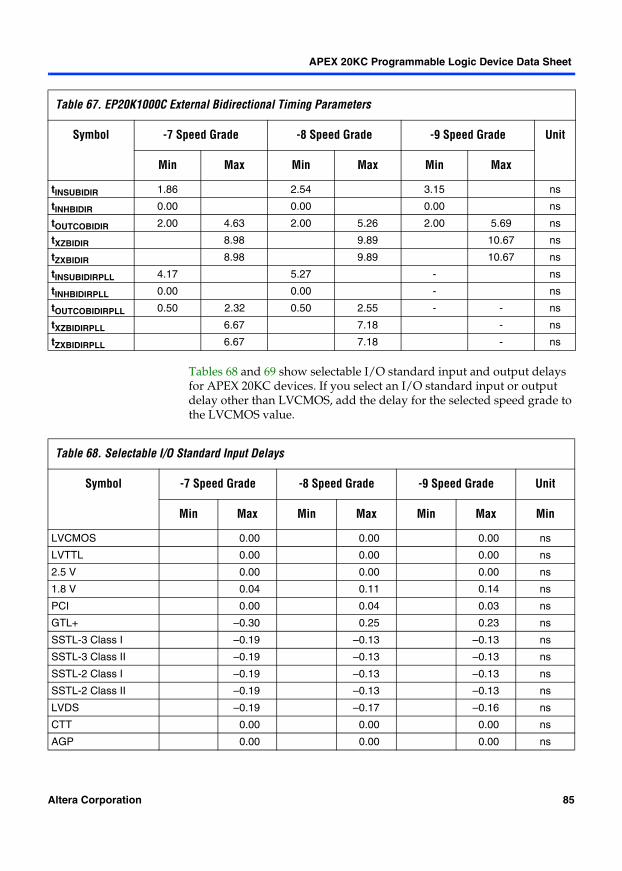
APEX 20KC Programmable Logic Device Data Sheet
Tables 68 and 69 show selectable I/O standard input and output delays for APEX 20KC devices. If you select an I/O standard input or output delay other than LVCMOS, add the delay for the selected speed grade to the LVCMOS value.
Table 67. EP20K1000C External Bidirectional Timing Parameters
Symbol -7 Speed Grade -8 Speed Grade -9 Speed Grade Unit
Min Max Min Max Min Max
tINSUBIDIR 1.86 2.54 3.15 ns
tINHBIDIR 0.00 0.00 0.00 ns
tOUTCOBIDIR 2.00 4.63 2.00 5.26 2.00 5.69 ns
tXZBIDIR 8.98 9.89 10.67 ns
tZXBIDIR 8.98 9.89 10.67 ns
tINSUBIDIRPLL 4.17 5.27 - ns
tINHBIDIRPLL 0.00 0.00 - ns
tOUTCOBIDIRPLL 0.50 2.32 0.50 2.55 - - ns
tXZBIDIRPLL 6.67 7.18 - ns
tZXBIDIRPLL 6.67 7.18 - ns
Table 68. Selectable I/O Standard Input Delays
Symbol -7 Speed Grade -8 Speed Grade -9 Speed Grade Unit
Min Max Min Max Min Max Min
LVCMOS 0.00 0.00 0.00 ns
LVTTL 0.00 0.00 0.00 ns
2.5 V 0.00 0.00 0.00 ns
1.8 V 0.04 0.11 0.14 ns
PCI 0.00 0.04 0.03 ns
GTL+ –0.30 0.25 0.23 ns
SSTL-3 Class I –0.19 –0.13 –0.13 ns
SSTL-3 Class II –0.19 –0.13 –0.13 ns
SSTL-2 Class I –0.19 –0.13 –0.13 ns
SSTL-2 Class II –0.19 –0.13 –0.13 ns
LVDS –0.19 –0.17 –0.16 ns
CTT 0.00 0.00 0.00 ns
AGP 0.00 0.00 0.00 ns
Altera Corporation 85
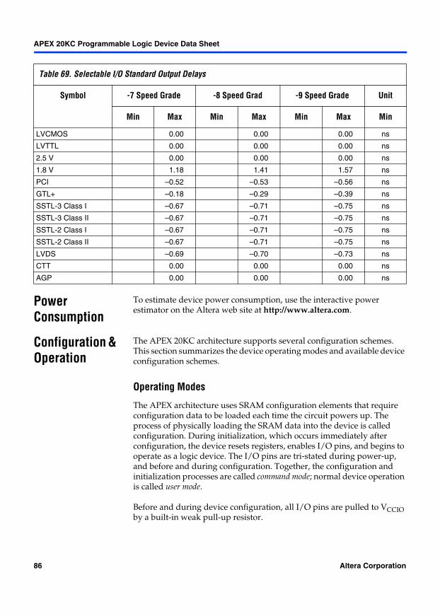
APEX 20KC Programmable Logic Device Data Sheet
Power Consumption
To estimate device power consumption, use the interactive power estimator on the Altera web site at http://www.altera.com.
Configuration & Operation
The APEX 20KC architecture supports several configuration schemes. This section summarizes the device operating modes and available device configuration schemes.
Operating Modes
The APEX architecture uses SRAM configuration elements that require configuration data to be loaded each time the circuit powers up. The process of physically loading the SRAM data into the device is called configuration. During initialization, which occurs immediately after configuration, the device resets registers, enables I/O pins, and begins to operate as a logic device. The I/O pins are tri-stated during power-up, and before and during configuration. Together, the configuration and initialization processes are called command mode; normal device operation is called user mode.
Before and during device configuration, all I/O pins are pulled to VCCIO by a built-in weak pull-up resistor.
Table 69. Selectable I/O Standard Output Delays
Symbol -7 Speed Grade -8 Speed Grad -9 Speed Grade Unit
Min Max Min Max Min Max Min
LVCMOS 0.00 0.00 0.00 ns
LVTTL 0.00 0.00 0.00 ns
2.5 V 0.00 0.00 0.00 ns
1.8 V 1.18 1.41 1.57 ns
PCI –0.52 –0.53 –0.56 ns
GTL+ –0.18 –0.29 –0.39 ns
SSTL-3 Class I –0.67 –0.71 –0.75 ns
SSTL-3 Class II –0.67 –0.71 –0.75 ns
SSTL-2 Class I –0.67 –0.71 –0.75 ns
SSTL-2 Class II –0.67 –0.71 –0.75 ns
LVDS –0.69 –0.70 –0.73 ns
CTT 0.00 0.00 0.00 ns
AGP 0.00 0.00 0.00 ns
86 Altera Corporation
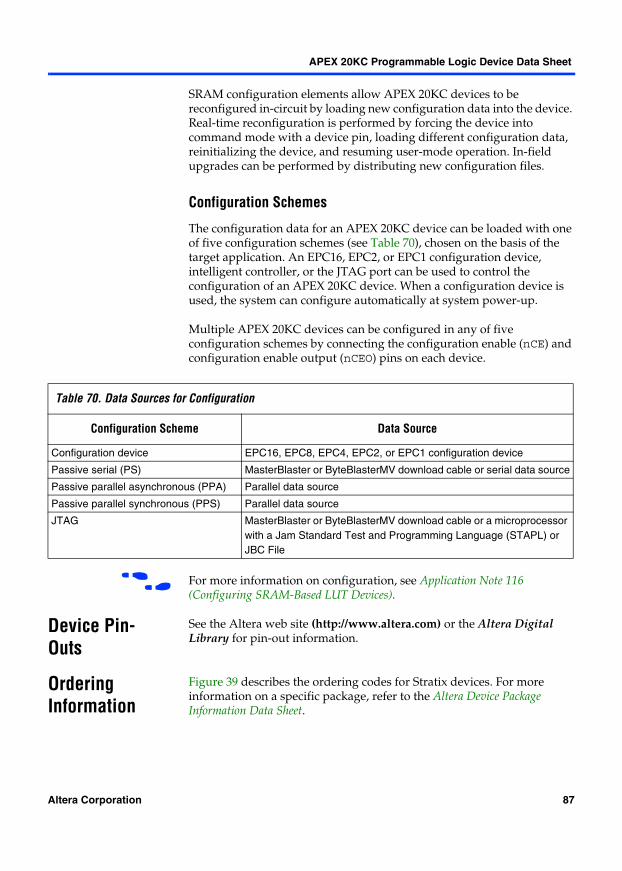
APEX 20KC Programmable Logic Device Data Sheet
SRAM configuration elements allow APEX 20KC devices to be reconfigured in-circuit by loading new configuration data into the device. Real-time reconfiguration is performed by forcing the device into command mode with a device pin, loading different configuration data, reinitializing the device, and resuming user-mode operation. In-field upgrades can be performed by distributing new configuration files.
Configuration Schemes
The configuration data for an APEX 20KC device can be loaded with one of five configuration schemes (see Table 70), chosen on the basis of the target application. An EPC16, EPC2, or EPC1 configuration device, intelligent controller, or the JTAG port can be used to control the configuration of an APEX 20KC device. When a configuration device is used, the system can configure automatically at system power-up.
Multiple APEX 20KC devices can be configured in any of five configuration schemes by connecting the configuration enable (nCE) and configuration enable output (nCEO) pins on each device.
f For more information on configuration, see Application Note 116 (Configuring SRAM-Based LUT Devices).
Device Pin-Outs
See the Altera web site (http://www.altera.com) or the Altera Digital Library for pin-out information.
Ordering Information
Figure 39 describes the ordering codes for Stratix devices. For more information on a specific package, refer to the Altera Device Package Information Data Sheet.
Table 70. Data Sources for Configuration
Configuration Scheme Data Source
Configuration device EPC16, EPC8, EPC4, EPC2, or EPC1 configuration device
Passive serial (PS) MasterBlaster or ByteBlasterMV download cable or serial data source
Passive parallel asynchronous (PPA) Parallel data source
Passive parallel synchronous (PPS) Parallel data source
JTAG MasterBlaster or ByteBlasterMV download cable or a microprocessor with a Jam Standard Test and Programming Language (STAPL) or JBC File
Altera Corporation 87
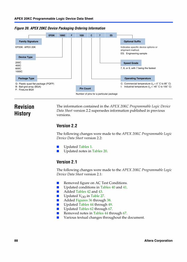
APEX 20KC Programmable Logic Device Data Sheet
Figure 39. APEX 20KC Device Packaging Ordering Information
Revision History
The information contained in the APEX 20KC Programmable Logic Device Data Sheet version 2.2 supersedes information published in previous versions.
Version 2.2
The following changes were made to the APEX 20KC Programmable Logic Device Data Sheet version 2.2:
Updated Tables 1. Updated notes in Tables 20.
Version 2.1
The following changes were made to the APEX 20KC Programmable Logic Device Data Sheet version 2.1:
Removed figure on AC Test Conditions. Updated conditions in Tables 40 and 41. Added Tables 42 and 43. Updated VOD in Table 27. Added Figures 36 through 38. Updated Tables 44 through 49. Updated Tables 62 through 67. Removed notes in Tables 44 through 67. Various textual changes throughout the document.
Device Type
Package Type
7, 8, or 9, with 7 being the fastest
Number of pins for a particular package
ES:
Q:B:F:
Plastic quad flat package (PQFP)Ball-grid array (BGA)FineLine BGA
EP20K: APEX 20K
200C400C600C1000C
C:I:
Commercial temperature (tJ = 0˚ C to 85˚ C)Industrial temperature (tJ = -40˚ C to 100˚ C)
Optional SuffixFamily Signature
Operating Temperature
Speed Grade
Pin Count
Engineering sample
7EP20K 1000C C1020F ES
Indicates specific device options or shipment method.
88 Altera Corporation

APEX 20KC Programmable Logic Device Data Sheet
Altera Corporation 89
APEX 20KC Programmable Logic Device Data Sheet
Copyright © 2002 Altera Corporation. All rights reserved. Altera, The Programmable Solutions Company, thestylized Altera logo, specific device designations, and all other words and logos that are identified astrademarks and/or service marks are, unless noted otherwise, the trademarks and service marks of AlteraCorporation in the U.S. and other countries. All other product or service names are the property of theirrespective holders. Altera products are protected under numerous U.S. and foreign patents and pendingapplications, mask work rights, and copyrights. Altera warrants performance of its semiconductor productsto current specifications in accordance with Altera’s standard warranty, but reserves theright to make changes to any products and services at any time without notice. Alteraassumes no responsibility or liability arising out of the application or use of anyinformation, product, or service described herein except as expressly agreed to in writingby Altera Corporation. Altera customers are advised to obtain the latest version of devicespecifications before relying on any published information and before placing orders forproducts or services.
101 Innovation DriveSan Jose, CA 95134(408) 544-7000http://www.altera.comApplications Hotline:(800) 800-EPLDCustomer Marketing:(408) 544-7104Literature Services:[email protected]
®
90 Altera Corporation


![Blank Document · Web viewComponent Quantity Information Altera EPF8452AQC160-3 1 Programmable Logic Device. [Ref. 18] Altera EPC1064LC20 1 EPROM. One Time Programmable package. [Ref](https://img.pdfslide.us/doc/110x75/5abb2dd47f8b9a441d8c8409/blank-document-viewcomponent-quantity-information-altera-epf8452aqc160-3-1-programmable.jpg)