Embed Size (px)
Citation preview
ProgrammableProgrammable LogicLogic DesignDesign
Grzegorz BudzyGrzegorz Budzyńń
LLectureecture 10:10:FPGA FPGA clockingclocking schemesschemes
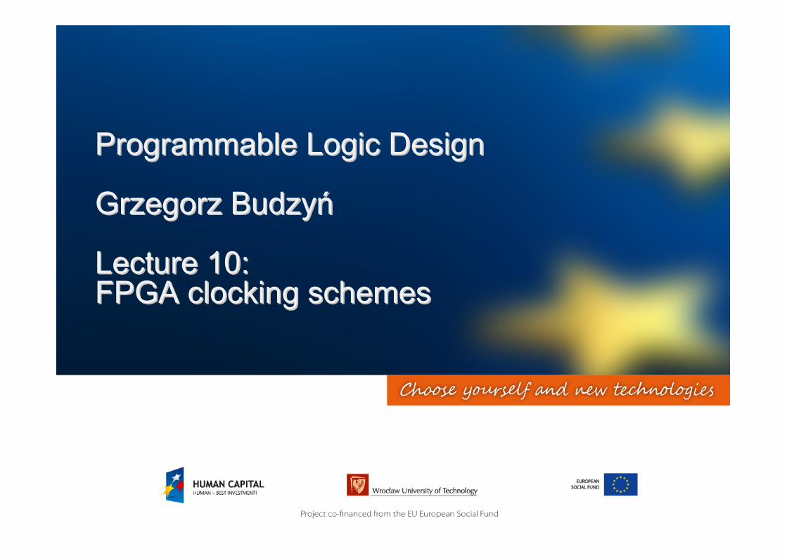
Plan
• Introduction
• Definitions
– Clock skew
– Metastability
• FPGA clocking resources
– DCM
– PLL
Introduction
• One of the most important steps in the design process is to identify how many different clocks to use and how to route them
Introduction• As larger designs are implemented in FPGAs, it is
likely that many of them will have multiple data paths running on multiple clocks
• An FPGA design that contains multiple clocks requires special attention
• Issues to focus on are:– maximum clock rates and skew,
– maximum number of clocks,
– asynchronous clock design,
– clock/data relationships.
Definitions
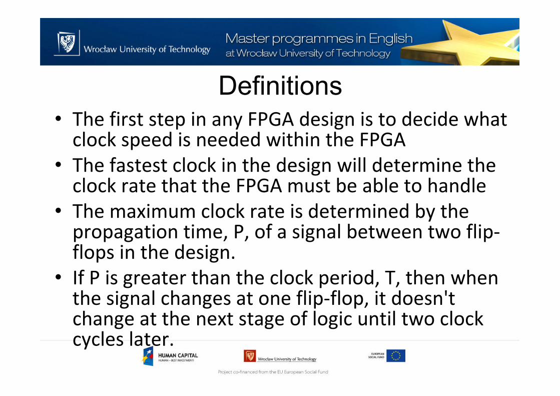
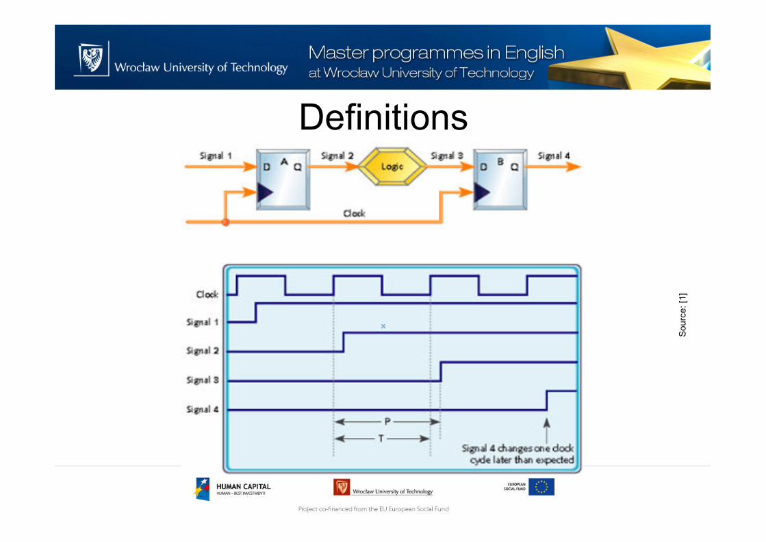
Definitions• The first step in any FPGA design is to decide what
clock speed is needed within the FPGA
• The fastest clock in the design will determine the clock rate that the FPGA must be able to handle
• The maximum clock rate is determined by the propagation time, P, of a signal between two flip-flops in the design.
• If P is greater than the clock period, T, then when the signal changes at one flip-flop, it doesn't change at the next stage of logic until two clock cycles later.
Definitions
Sourc
e: [1
]
Definitions• The propagation time is the sum of:
– the hold time required for the signal to change at the output of the first flip-flop,
– the delay of any combinatorial logic between stages,
– the routing delay between stages,
– the set-up time for the signal going into the flip-flop at the second stage.
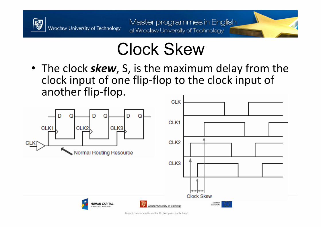
Clock Skew• The clock skew, S, is the maximum delay from the
clock input of one flip-flop to the clock input of another flip-flop.
Clock Skew
Sourc
e: [1
]
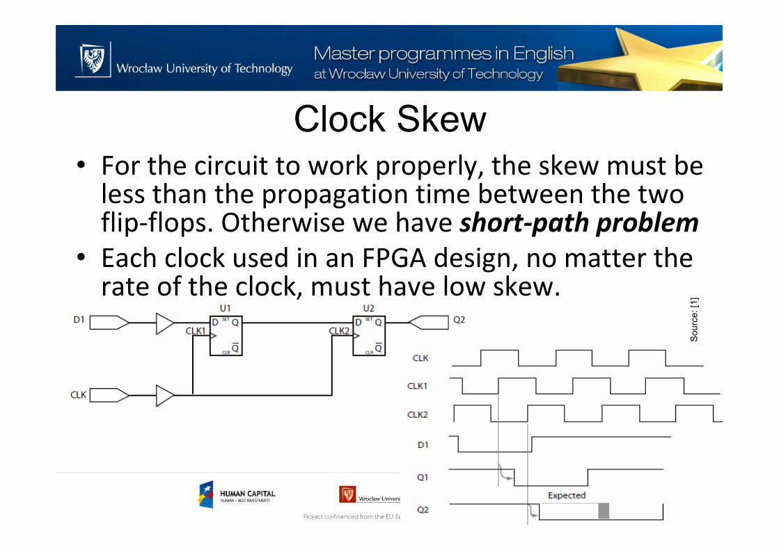
• For the circuit to work properly, the skew must be less than the propagation time between the two flip-flops. Otherwise we have short-path problem
• Each clock used in an FPGA design, no matter the rate of the clock, must have low skew.
Clock Skew - reduction
• The short-path problem is created by the
existence of an unacceptably large clock skew
• Minimizing the clock skew is the best approach
to reduce the risk of short-path problems
• The best way to minimize the clock skew is to
use hardware resources like Delay Locked Loop
or global clock networks
Clock Skew - reduction
• In cases where designs include multiple clock
domains, there may not be enough low-skew
global resources in the targeted FPGA for all the
external/internal clock signals
• Therefore, regular routing resources and buffers
are used to build clock trees for the clock
network – possibility of a noticable clock skew
Clock Skew - reduction
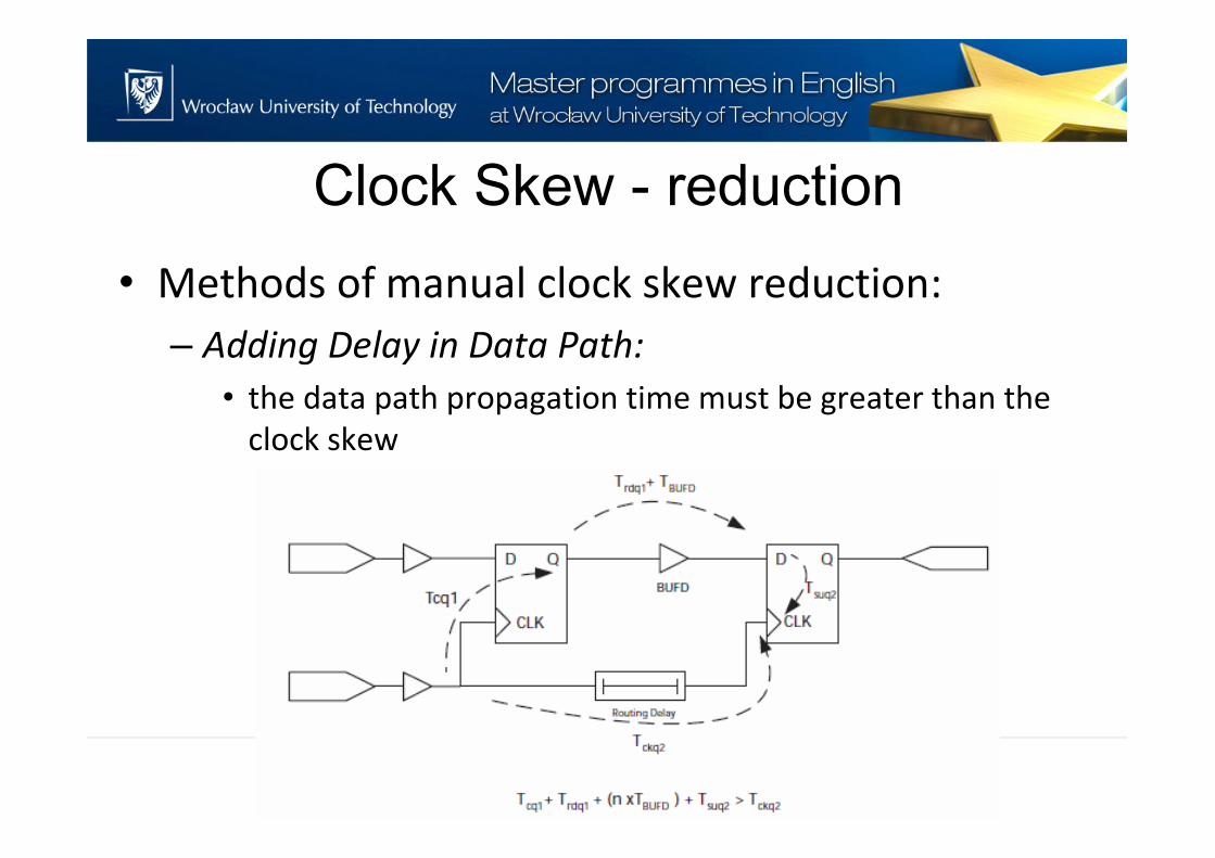
• Methods of manual clock skew reduction:
– Adding Delay in Data Path:
• the data path propagation time must be greater than the
clock skew
Clock Skew - reduction
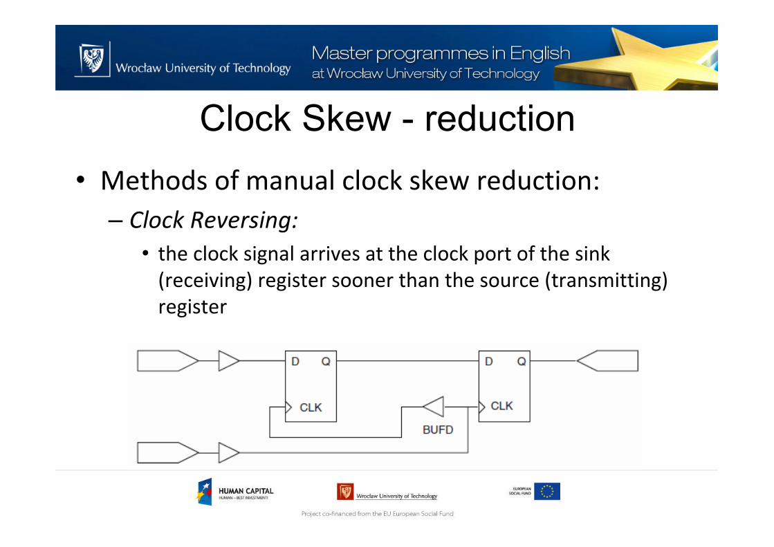
• Methods of manual clock skew reduction:
– Clock Reversing:
• the clock signal arrives at the clock port of the sink
(receiving) register sooner than the source (transmitting)
register
Clock Skew - reduction
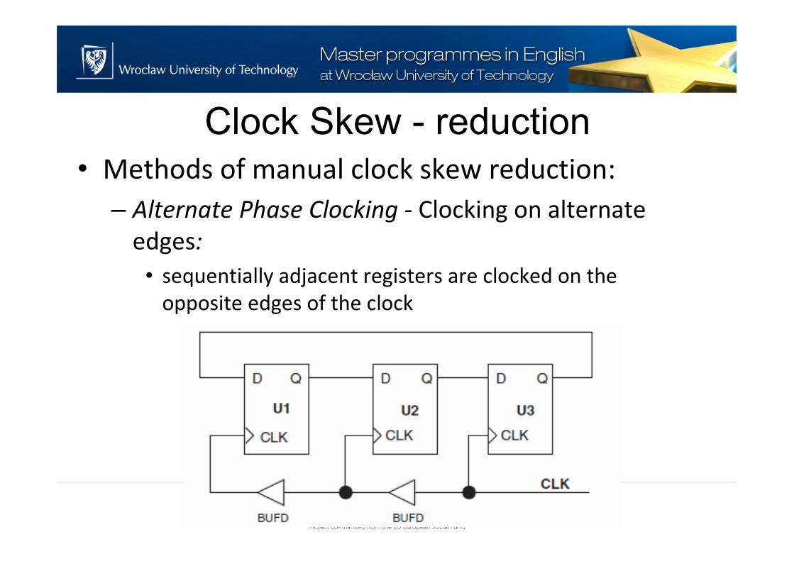
• Methods of manual clock skew reduction:
– Alternate Phase Clocking - Clocking on alternate
edges:
• sequentially adjacent registers are clocked on the
opposite edges of the clock
Clock Skew - reduction
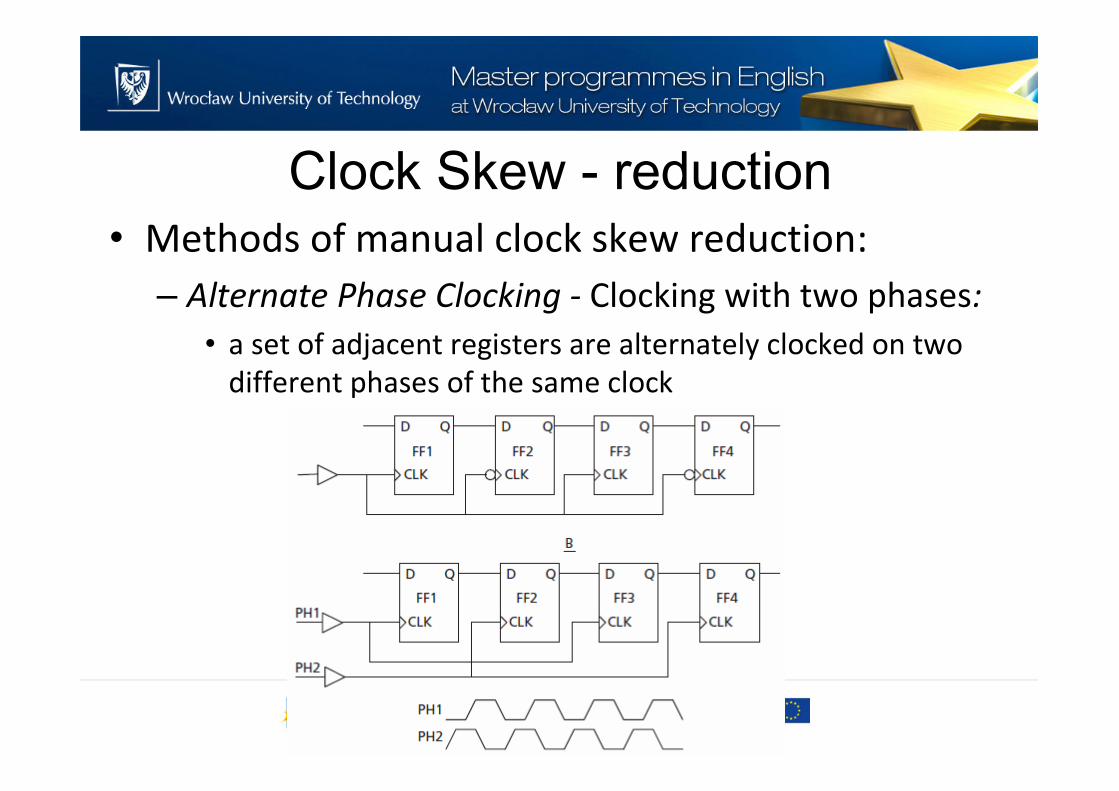
• Methods of manual clock skew reduction:
– Alternate Phase Clocking - Clocking with two phases:
• a set of adjacent registers are alternately clocked on two
different phases of the same clock
Metastability• One of the most serious problems associated with
multiple clock designs is when two stages of logic are combined using asynchronous clocks
• Asynchronous logic can create metastable states that can seriously degrade the performance of the design or completely destroy the functionality.
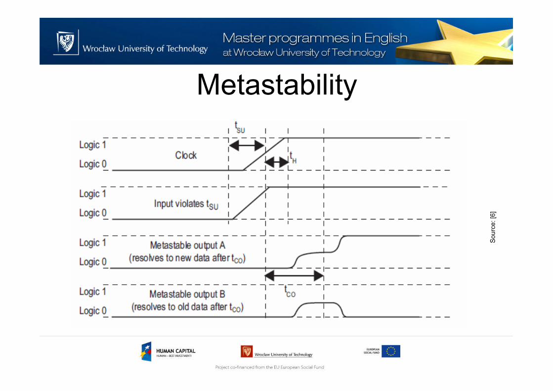
Metastability• A metastable state is created when the flip-flop's
timing requirements (setup and hold times) are violated.
• The resulting output of the flip-flop is unknown, and can make the entire design nondeterministic.
• If one stage of logic asynchronously feeds data to another, it is difficult, if not impossible to meet the set-up and hold-time requirements of the flip-flop.
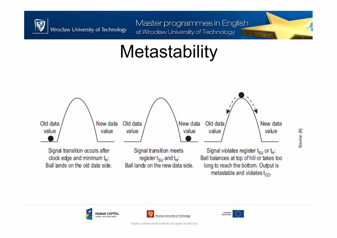
Metastability
Sourc
e: [6
]
Metastability
Sourc
e: [6
]
Metastability• One of the metastability solution is the double-
registering technique.
• Data coming into the first flip-flop is asynchronous with the clock, so the first flip-flop will almost certainly go metastable.
• However, the second flip-flop will never go metastable as long as the length of metastability is less than the period of the clock. (Unfortunately, FPGA vendors rarely publish metastability times, though they are typically less than the sum of the set-up and hold time of the flip-flop.)
Metastability
Sourc
e: [5
]
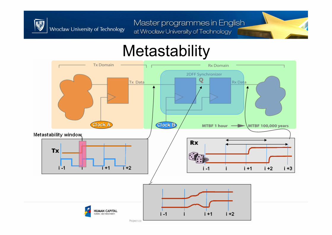
Metastability• If the clock is not too fast to meet normal timing
constraints, it is probably not going to propagate metastable states in a circuit shown.
• Even though the output of the first flip-flop can be used as long as all of the paths out go to flip-flops clocked by the same clock, it is generally good practice to use a circuit such as shown to isolate metastability to one short line.
• That way, it is less likely that a future change to the circuit will unintentionally use the metastableline in nonclocked logic.
FPGA clocking resources(Spartan 6)
Clocking resources
• Each Spartan-6 FPGA device includes 16 high-speed, low-skew global clock resources
• Each Spartan-6 FPGA also provides 40 ultra high-
speed, low-skew I/O regional clock resources
• These resources are used automatically by theXilinx tools
Clocking resources
• The Spartan-6 FPGA clock resources consist of:– Clock networks:
• Global clock network driven by global clock multiplexers (BUFGMUX):
– can multiplex between two global clock sources or be used as a simple BUFG clock buffer.
• I/O regional clock networks driven by I/O clock buffers (BUFIO2) as well as PLL clock buffers (BUFPLL):
– used to drive clocks routed only on the I/O regional clock network with much higher performance than the global clock network
Clocking resources• The Spartan-6 FPGA clock resources consist of:
– Connections:• Global clock input pads (GCLK)
• Global clock multiplexers (BUFG, BUFGMUX)
• I/O clock buffers (BUFIO2, BUFIO2_2CLK, BUFPLL)
• Clock routing buffers (BUFH)
– Auxiliary blocks:• CMT – Clock Management Tiles
• DCM – Digital Clock Management– DLL – Delay Locked Loop
– DFS – Digital Frequency Synthesiser
– DPS – Digital Phase Synthesiser
• PLL – Phase Locked Loop
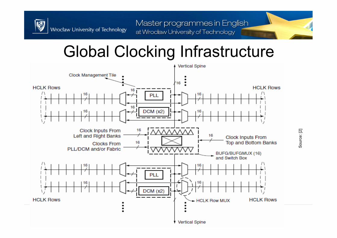
Global Clocking Infrastructure
Sourc
e: [2
]
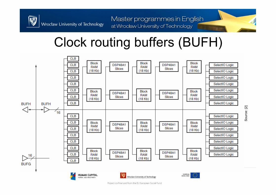
Clock routing buffers (BUFH)
Sourc
e: [2
]
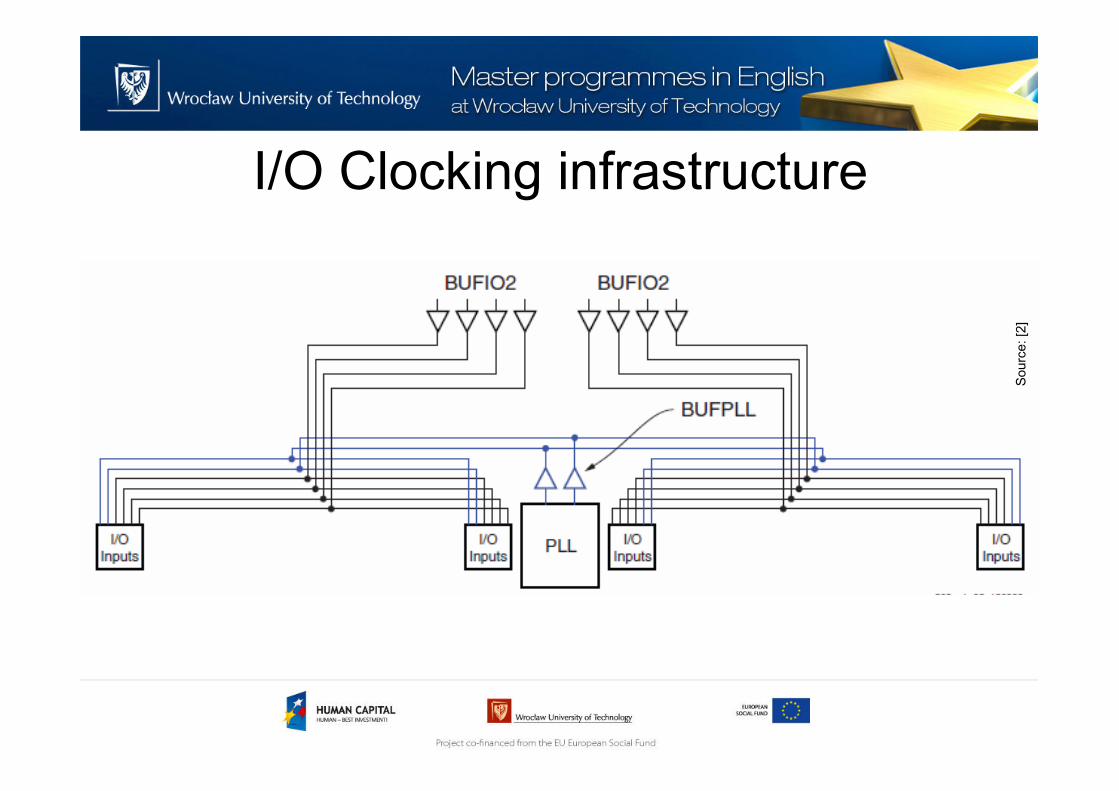
I/O Clocking infrastructure
Sourc
e: [2
]
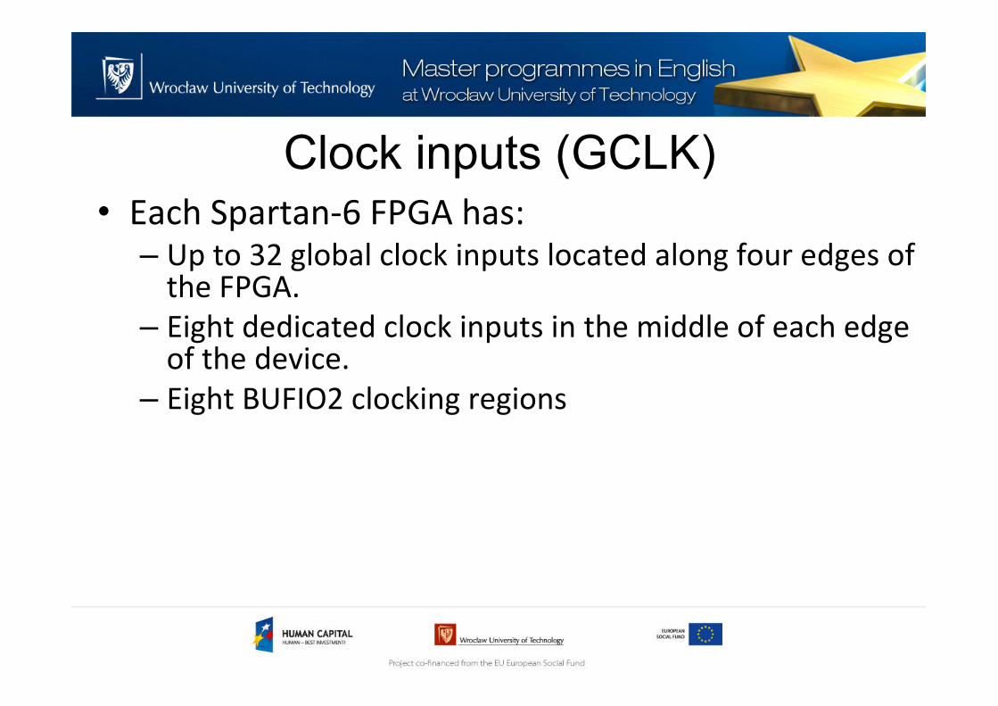
Clock inputs (GCLK)• Each Spartan-6 FPGA has:
– Up to 32 global clock inputs located along four edges of the FPGA.
– Eight dedicated clock inputs in the middle of each edge of the device.
– Eight BUFIO2 clocking regions
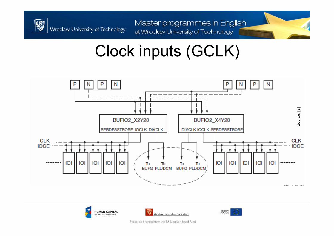
Clock inputs (GCLK)
Sourc
e: [2
]
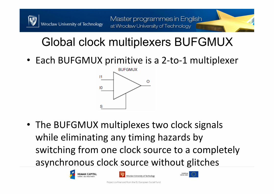
Global clock multiplexers BUFGMUX
• Each BUFGMUX primitive is a 2-to-1 multiplexer
• The BUFGMUX multiplexes two clock signals
while eliminating any timing hazards by
switching from one clock source to a completely
asynchronous clock source without glitches

Global clock multiplexers BUFGMUX
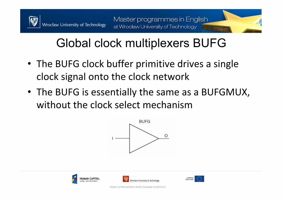
Global clock multiplexers BUFG
• The BUFG clock buffer primitive drives a single
clock signal onto the clock network
• The BUFG is essentially the same as a BUFGMUX,
without the clock select mechanism
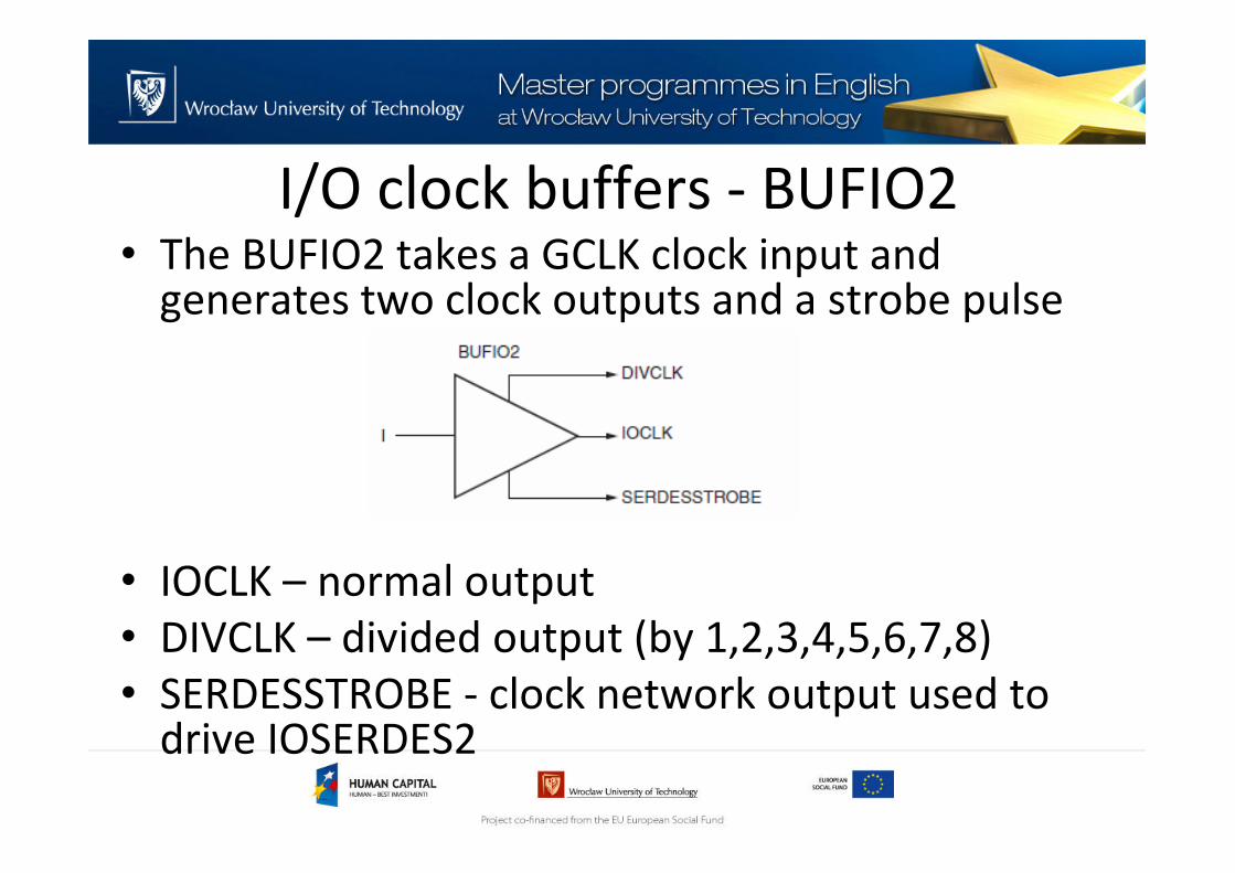
I/O clock buffers - BUFIO2• The BUFIO2 takes a GCLK clock input and
generates two clock outputs and a strobe pulse
• IOCLK – normal output
• DIVCLK – divided output (by 1,2,3,4,5,6,7,8)
• SERDESSTROBE - clock network output used to drive IOSERDES2
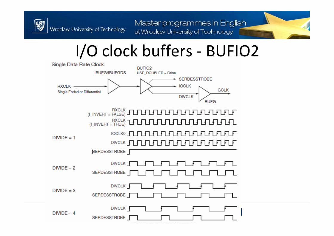
I/O clock buffers - BUFIO2
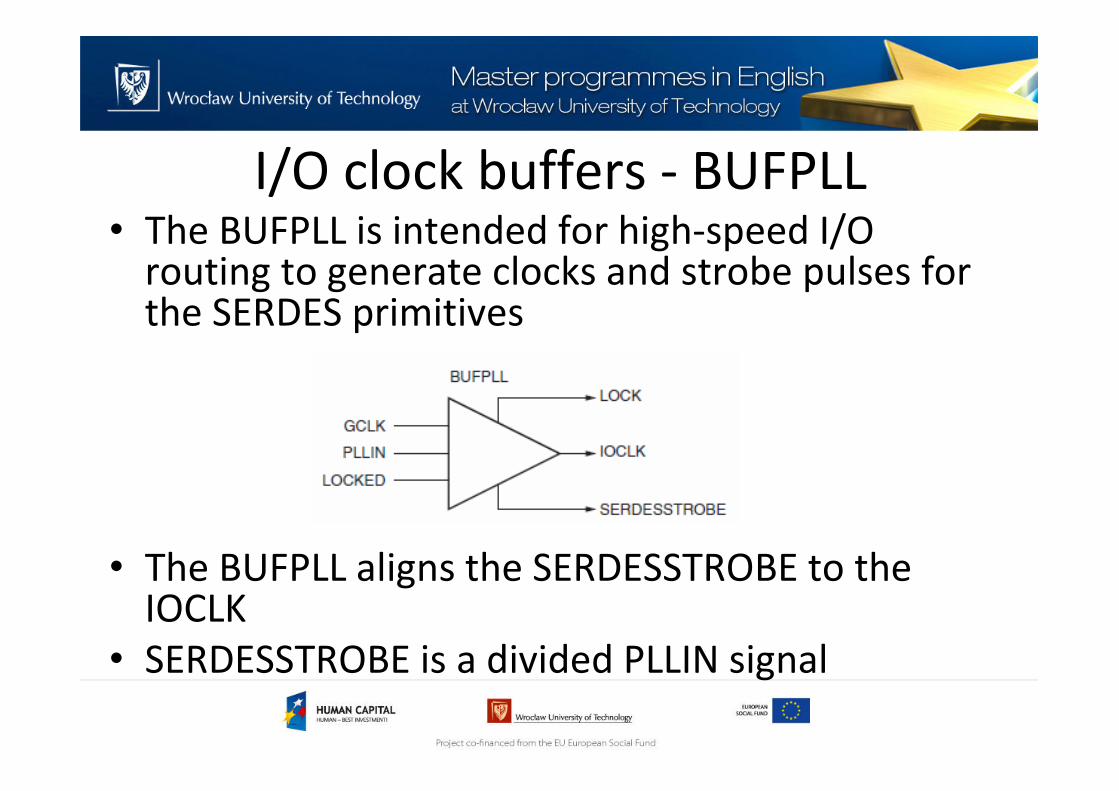
I/O clock buffers - BUFPLL• The BUFPLL is intended for high-speed I/O
routing to generate clocks and strobe pulses for the SERDES primitives
• The BUFPLL aligns the SERDESSTROBE to theIOCLK
• SERDESSTROBE is a divided PLLIN signal
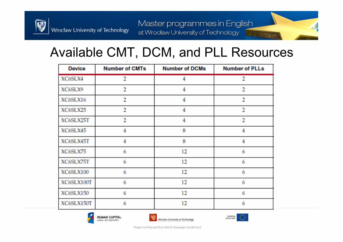
Available CMT, DCM, and PLL Resources

DCM
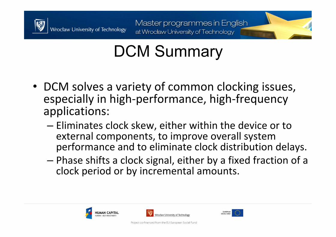
DCM Summary
• Digital Clock Managers (DCMs) provide advanced clocking capabilities to Spartan FPGA applications
• DCMs integrate advanced clocking capabilities directly into the global clock distribution network.
DCM Summary
• DCM solves a variety of common clocking issues, especially in high-performance, high-frequency applications:– Eliminates clock skew, either within the device or to
external components, to improve overall system performance and to eliminate clock distribution delays.
– Phase shifts a clock signal, either by a fixed fraction of a clock period or by incremental amounts.
DCM Summary
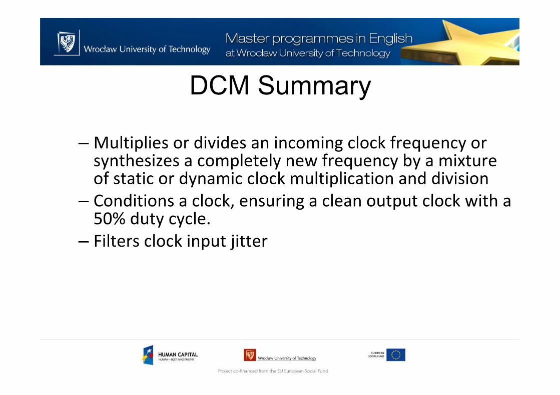
– Multiplies or divides an incoming clock frequency or synthesizes a completely new frequency by a mixture of static or dynamic clock multiplication and division
– Conditions a clock, ensuring a clean output clock with a 50% duty cycle.
– Filters clock input jitter
DCM Summary
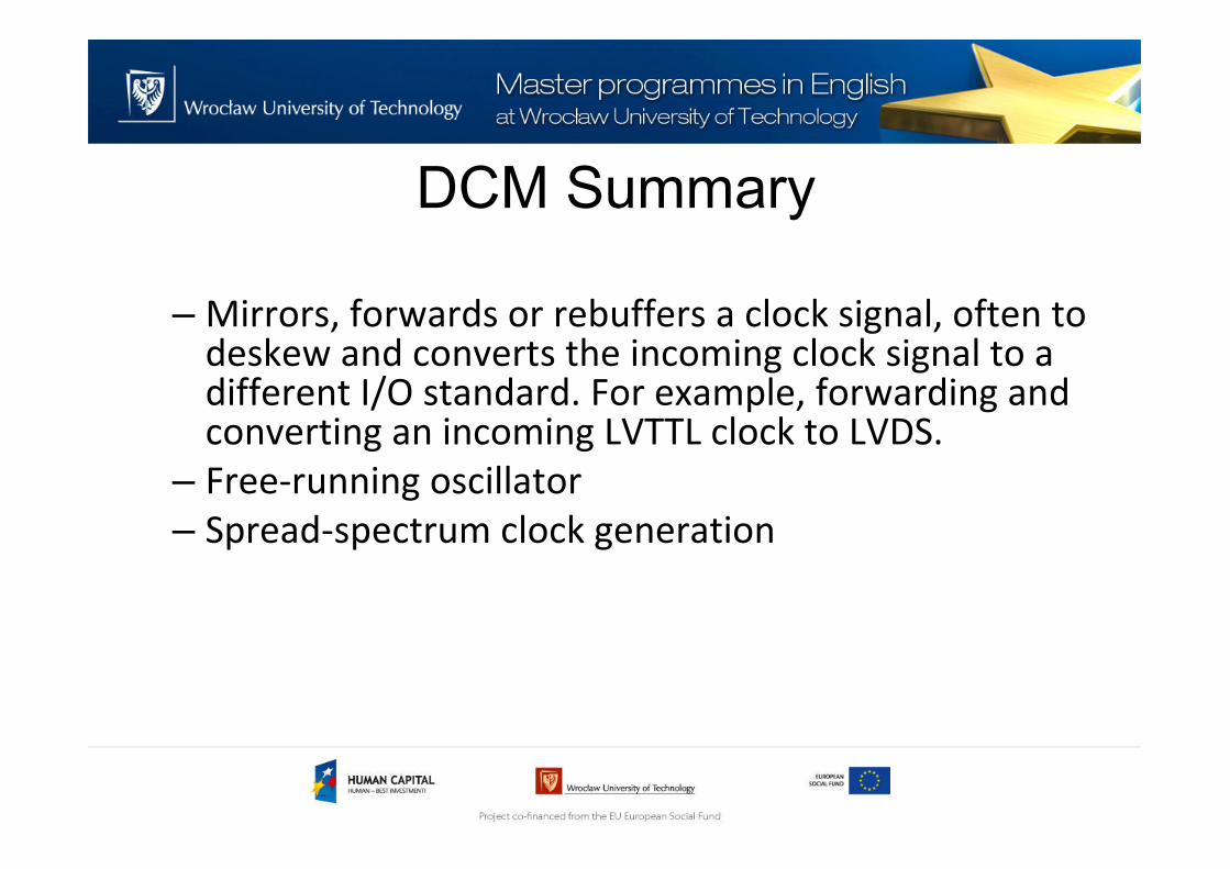
– Mirrors, forwards or rebuffers a clock signal, often to deskew and converts the incoming clock signal to a different I/O standard. For example, forwarding and converting an incoming LVTTL clock to LVDS.
– Free-running oscillator
– Spread-spectrum clock generation
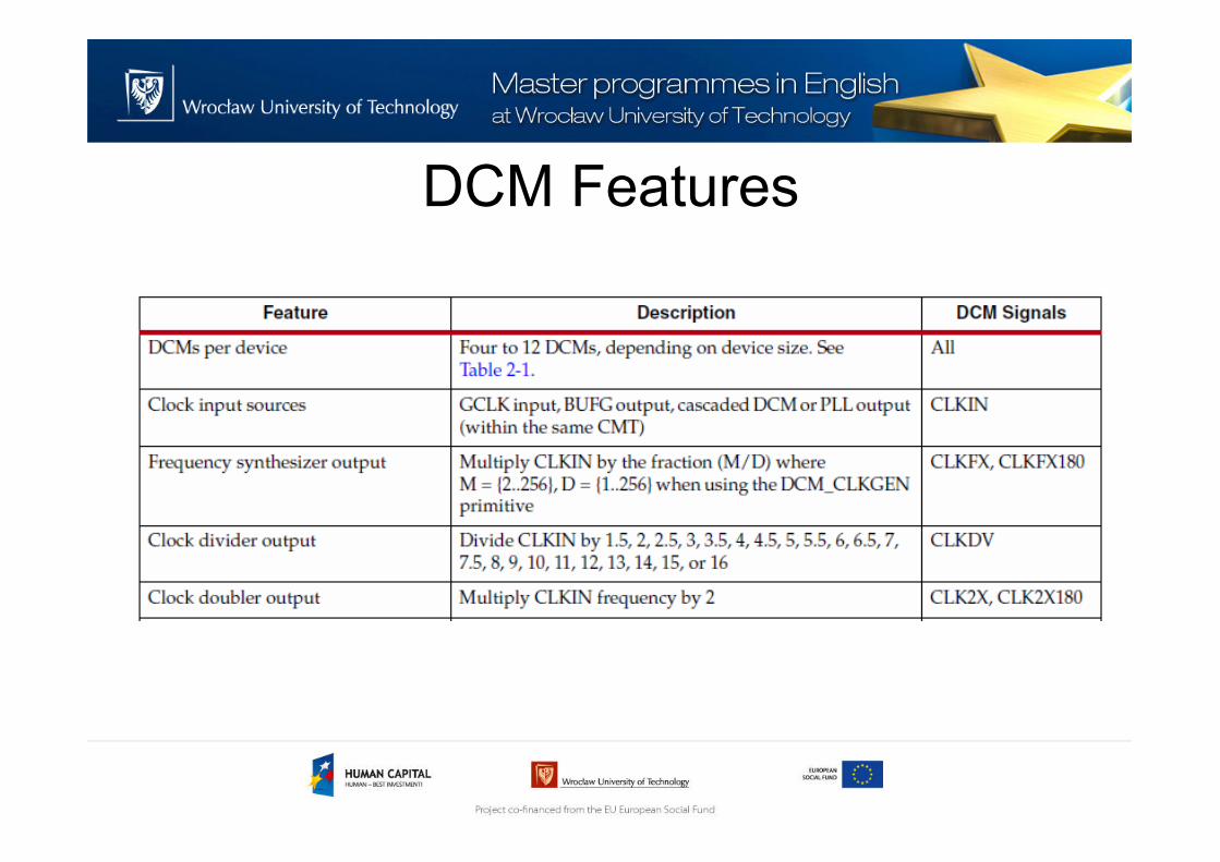
DCM Features
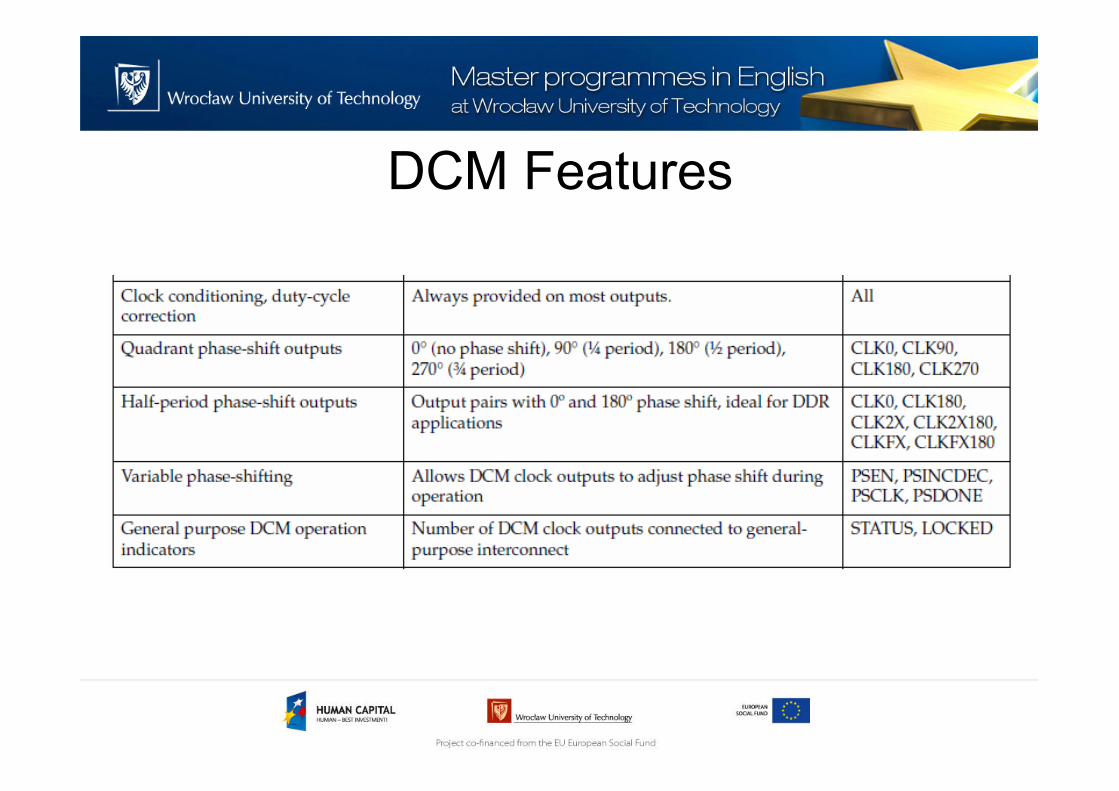
DCM Features
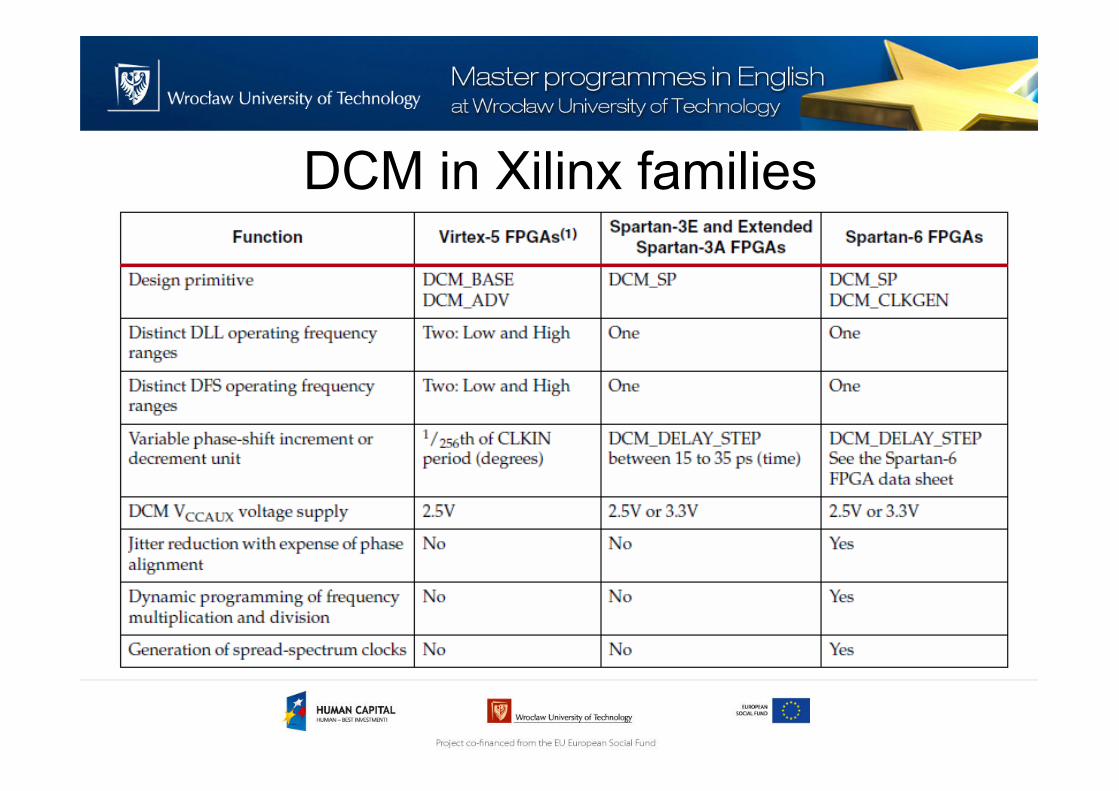
DCM in Xilinx families
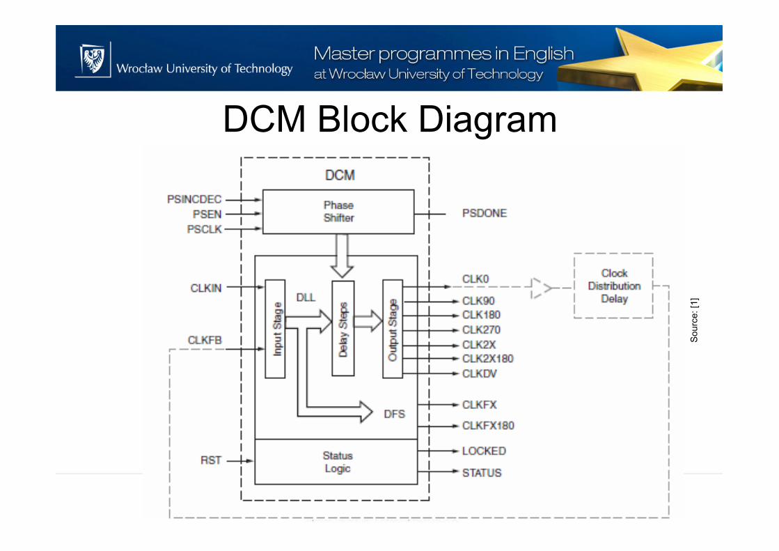
DCM Block Diagram
Sourc
e: [1
]
Delay-Locked Loop
• The Delay-Locked Loop (DLL) provides an on-chip digital deskew circuit that effectively generates clock output signals with a net zero delay.
• The deskew circuit compensates for the delay on the clock routing network by monitoring an output clock, from either the CLK0 or the CLK2X outputs
Delay-Locked Loop
• The DLL effectively eliminates delay from the external clock input port to the individual clock loads within the device.
• The well-buffered global network minimizes the clock skew on the network caused by loading differences.
Delay-Locked Loop - functioning• A DLL in its simplest form inserts a variable delay
line between the external clock and the internal clock
• The clock tree distributes the clock to all registers
and then back to the feedback pin of the DLL
• The control circuit of the DLL adjusts the delays so
that the rising edges of the feedback clock align
with the input clock
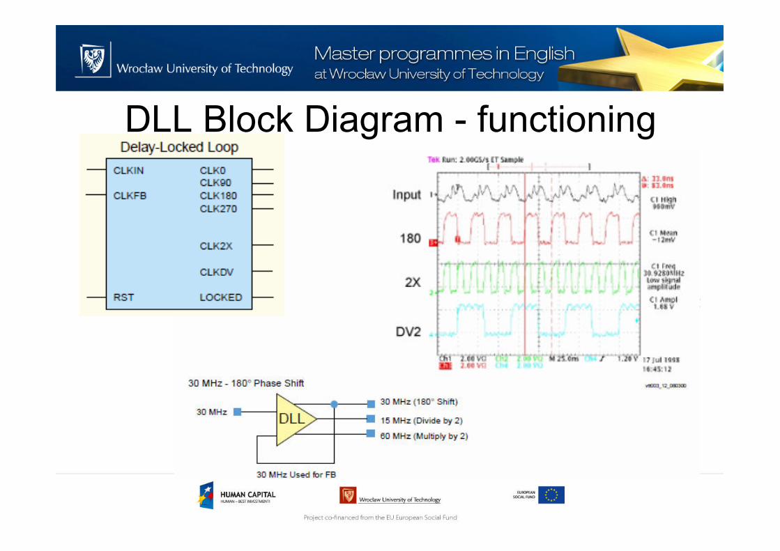
DLL Block Diagram - functioning
Sourc
e: [1
]
Digital Frequency Synthesizer
• The Digital Frequency Synthesizer (DFS) provides a wide and flexible range of output frequencies based on the ratio of two user-defined integers, a multiplier (CLKFX_MULTIPLY) and a divisor (CLKFX_DIVIDE).
• The output frequency is derived from the input clock (CLKIN) by simultaneous frequency division and multiplication.
• The DFS feature can be used in conjunction with or separately from the DLL feature of the DCM
Phase Shift
• The Phase Shift (PS) controls the phase relations of the DCM clock outputs to the CLKIN input.
• PS can be used in either fixed phase-shift or variable phase shift modes
• The phase of all nine DCM clock output signals are shifted by a fixed fraction of the input clock period when using the fixed phase shift.
• The PS also provides a digital interface for the FPGA application to dynamically advance or retard the current shift value, called variable phase shift.
Status Logic
• The status logic indicates the current state of the DCM via the LOCKED and STATUS[0] output signals.
• The LOCKED output signal indicates whether the DCM outputs are in phase with the CLKIN input.
• The STATUS output signals indicate the state of the DLL and PS operations.
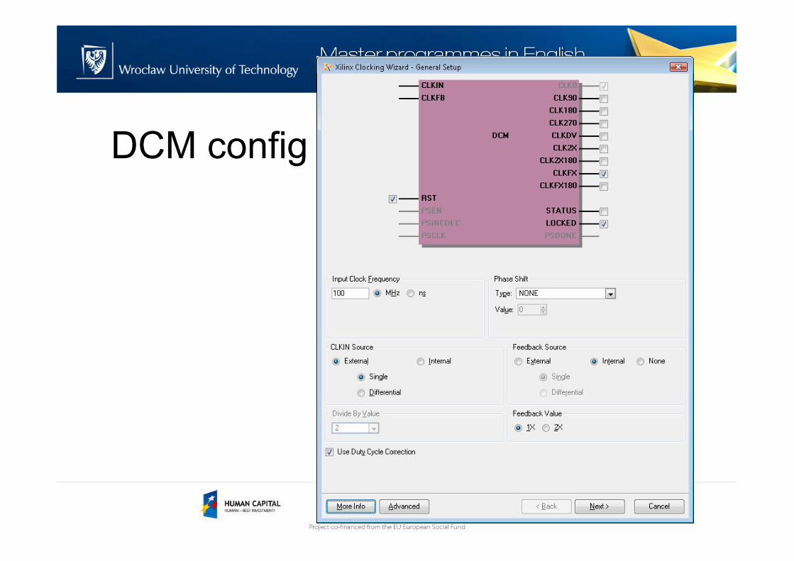
DCM config
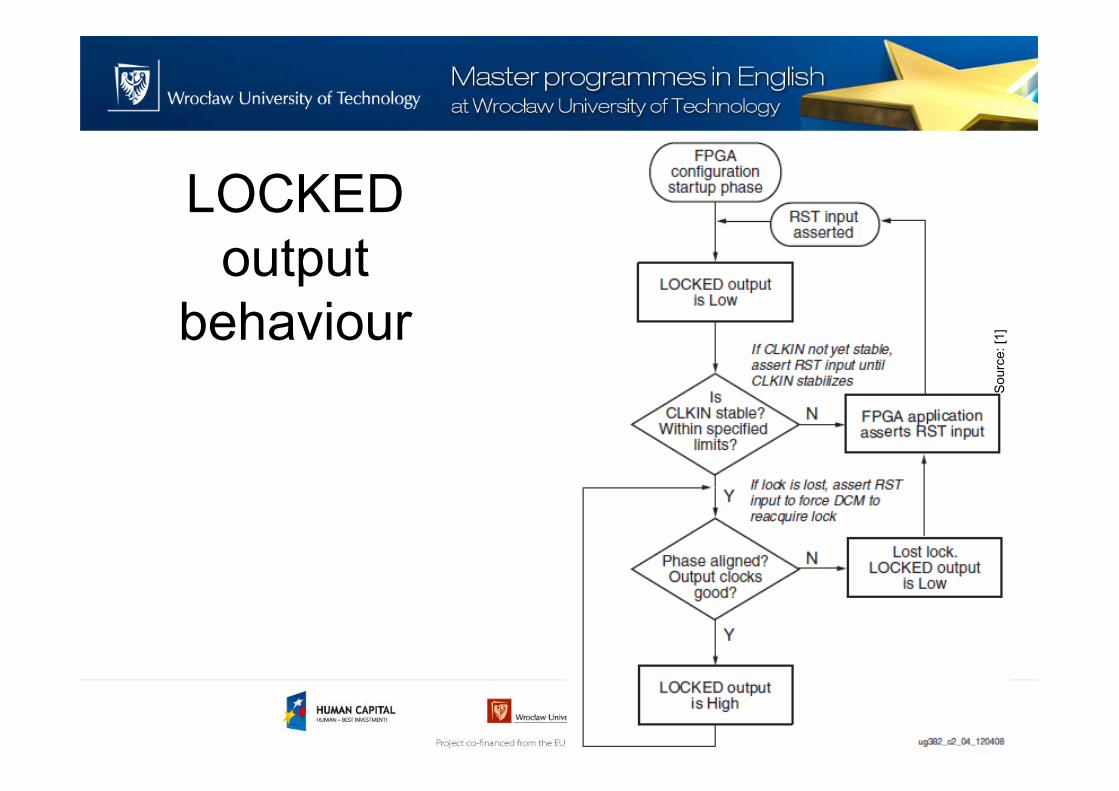
LOCKED
output
behaviour
Sourc
e: [1
]
Spread Spectrum Generation
• Spread-spectrum clock generation (SSCG) is widely used by manufacturers of electronic devices to reduce the spectral density of the electromagnetic interference (EMI) generated by these devices.
• Typical (but expensive!) solutions for meeting EMC requirements involve adding expensive shielding, ferrite beads, or chokes
Spread Spectrum Generation
• SSCG spreads the electromagnetic energy over a large frequency band to effectively reduce the electrical and magnetic field strengths measured within a narrow window of frequencies.
• The peak electromagnetic energy at any one frequency is reduced by modulating the SSCG output.
Spread Spectrum Generation
• The SSCG commonly defines the following parameters:– Frequency deviation, that is the percentage of the
input frequency
– Modulation frequency
– Spread type: up/down/center
– Modulation profile, for example, the shape of the triangle
• Typically: 75 MHz (input frequency), ±2.0% centerspread, and 75 KHz triangular modulation.
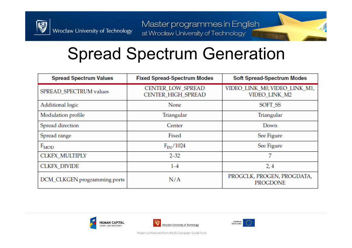
Spread Spectrum Generation
PLL
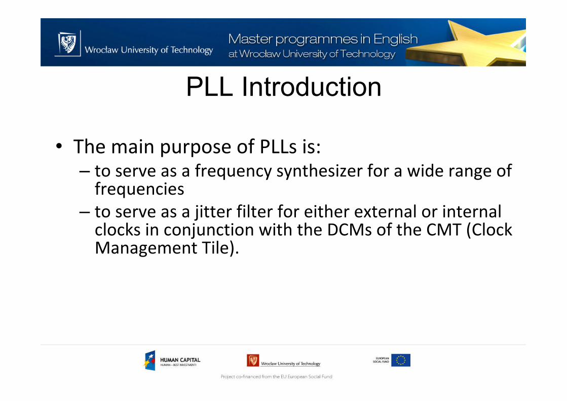
PLL Introduction
• The main purpose of PLLs is:– to serve as a frequency synthesizer for a wide range of
frequencies
– to serve as a jitter filter for either external or internal clocks in conjunction with the DCMs of the CMT (ClockManagement Tile).
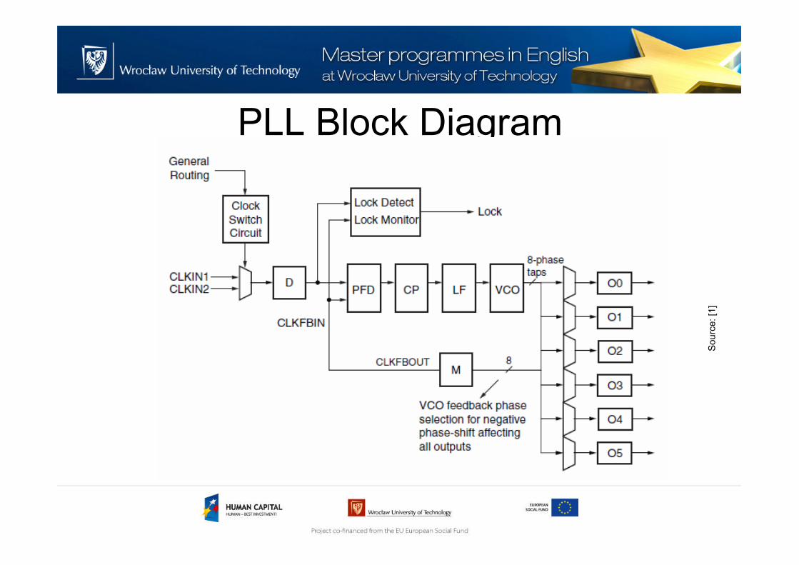
PLL Block Diagram
Sourc
e: [1
]
PLL Block Diagram
• D is a programmable counter for each clock input
• Phase-Frequency Detector (PFD) compares both phase and frequency of the input (reference) clock and the feedback clock– The PFD is used to generate a signal proportional to the
phase and frequency between the two clocks.
• Charge Pump (CP) and Loop Filter (LF) are used to generate a reference voltage to the Voltage Controlled Oscillator (VCO).
PLL Block Diagram
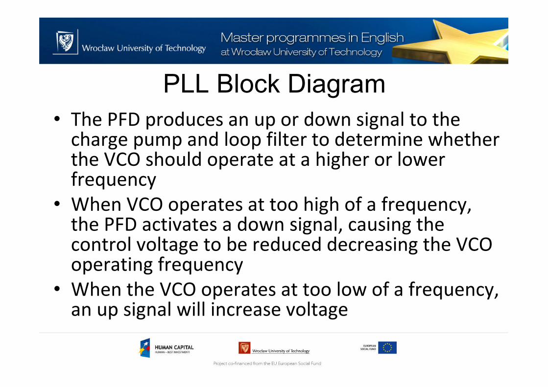
• The PFD produces an up or down signal to the charge pump and loop filter to determine whether the VCO should operate at a higher or lower frequency
• When VCO operates at too high of a frequency, the PFD activates a down signal, causing the control voltage to be reduced decreasing the VCO operating frequency
• When the VCO operates at too low of a frequency, an up signal will increase voltage
PLL Block Diagram
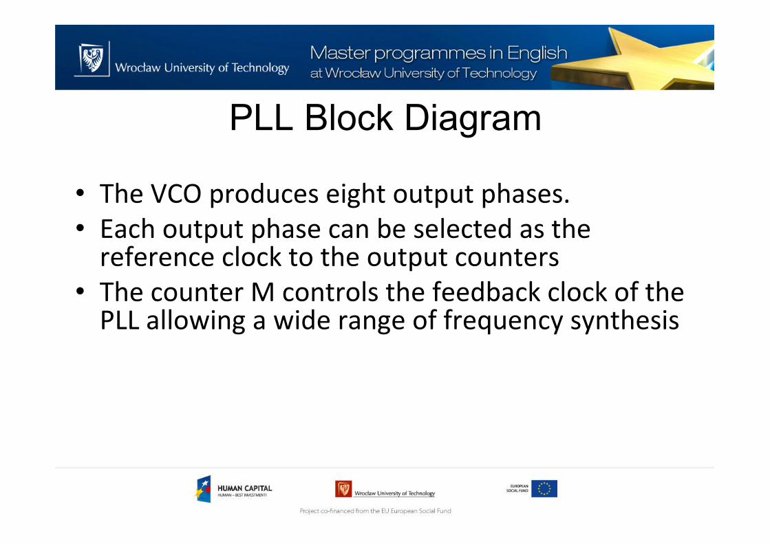
• The VCO produces eight output phases.
• Each output phase can be selected as the reference clock to the output counters
• The counter M controls the feedback clock of the PLL allowing a wide range of frequency synthesis
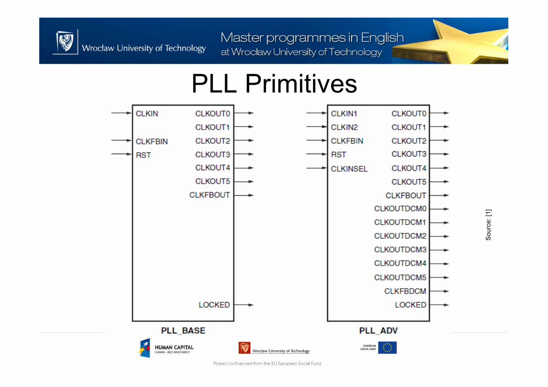
PLL Primitives
Sourc
e: [1
]
Thank you for your attention
References
[1] Tim Behne, „FPGA Clock Schemes”
[2] Spartan-6 family documentation; www.xilinx.com
[3] http://www.actel.com/documents/Clock_Skew_AN.pdf
[4] http://www.altera.com/literature/wp/wp-01082-quartus-ii-
metastability.pdf
[5]
http://www.xilinx.com/support/documentation/application_notes/
xapp094.pdf
[6]
https://nepp.nasa.gov/mapld_2009/talks/Posters/Landoll_David_m
apld09_pres_1.ppt#1019,12,Clock Domain Crossings Guaranteed to
Cause Metastability

![Applied Wireless Electronics Grzegorz Budzy ń Lecture 3 ... · PDF fileApplied Wireless Electronics Grzegorz Budzy ... ZigBee – Frequency range Source: [2] ... Message Integrity](https://img.pdfslide.us/doc/110x75/5ab819af7f8b9ac1058c4907/applied-wireless-electronics-grzegorz-budzy-n-lecture-3-wireless-electronics.jpg)