Embed Size (px)
Citation preview

The Ninth U.S.-Japan Seminar on
Dielectric and Piezoelectric Ceramics
PROGRAM AND EVALUATIONS
General Chairmen: Tadashi Takenaka (Science University of Tokyo, Japan) Thomas R. Shrout (The Pennsylvania State University, USA)
Program Chairmen: Takaaki Tsurumi (Tokyo Institute of Technology, Japan) Shoko Yoshikawa (Active Control experts, Inc., USA)
Financial Committee: Kazuo Miyabe (TDK Corp., Japan)
Administration: Michiko Fukutomi (Tokyo Institute of Technology, Japan)
DISTRIBUTION STATEMENT A Approved for Public Release
Distribution Unlimited
November 2-5, 1999 Pdzzan Sea Park Hotel, Tancha Bay
Okinawa, Japan
p<JIG QtJALIffY DfiwPECTED 1 20000120 013

TABLE OF CONTENTS
U.S. Chairman's Report iii
Abstract iii
Participants iii
U.S. Japan Seminar Evaluations vii
Dr. Donald M. Smyth ix
Dr. Jon-Paul Maria xv
Dr. David Cann xxi
Dr. Herbert Giesche xxvii
Dr. Yet-Ming Chiang xxx
List of Participants xxxi
Program and Extended Abstracts xxxiv
Report Document Page xxxxix

This work relates to Department of Navy Grant N00014-99-1-0138 issued by the Office of Naval Research. The United States Government has a royalty-free license throughout the world in all copyrightable material herein.
n
U.S. Chairman's Report
Abstract
The Ninth U.S.-Japan Seminar on Dielectric and Piezoelectric Ceramics was held on
Okinawa, Japan, through November 2-5, 1999. The local organization was from the Science
University of Tokyo and the Tokyo Institute of Technology. The total number of papers was
106: 69 Japanese and 37 U.S.; 40% of the papers were from industry.
The principal technical topics were: (1) Piezoelectric Ceramics (bulk), (2) Multilayer
Capacitors, and (3) Thin Film Dielectrics. The emphasis on multilayer capacitors was on base
metal electrodes (BME) with ultra thin layers (< 3 microns) and the search for non-PbO based
piezoelectrics a major thrust area in Japan. Novel pyrochlore and quantum ferroelectric
materials and improved understanding of polarization fatigue in thin films were highlighted.
Participants
The number of participants of the Ninth U.S.-Japan Seminar were the highest of all the
previous meetings, a point of contention, in that "bigger is not better", as commented on by
several of the evaluators. Of particular significance, however, was the -40% attendance rate of
U.S. industrial participants, up significantly in contrast to previous meetings, but no major bulk
piezoelectric manufacturer was represented.
Table I summarizes the participants as broken down into U.S. vs. Japan and industry vs.
university, the latter including government laboratories. Table JJ summarizes the general topics,
with Table III providing a list of industrial participants.
in

Table I. Participants of the Ninth U.S.-Japan Seminar on
Dielectric and Piezoelectric Ceramics
Total Number of Papers: 106
Japan: 69
U.S. 37
Industry:
Japan: 26 (-40%)
U.S.: 14 (-40%)
University:
Japan: 41
U.S.: 26
Table II. Participants of the U.S. -Japan Seminar by Topic Area
Japan U.S.
Industry University Industry University
Piezoelectrics (Bulk) 9 15 3 12
Multilayer Capacitors 9 3 7 4
Thin Films 7 20 2 8
Microwave Dielectrics 2 3 1 1
Misc.: Polymer Packaging (Kyocera)
IV

Table III. Industrial Participants of the Ninth U.S.-Japan Seminar
Japan U.S.
Piezoelectrics Ricoh Cerone TDK ACX Murata Hewlett Packard Fuji Electric
Multilayer Capacitors Murata Kernet TDK Degussa Taiyo Yuden TAM Ceramics Toshiba/Nippon-Chemicon Ferro Fuji Titanium Cabot Corp.
MRA Labs
Thin Films Rohm Co. IBM Mitsubishi Materials Motorola Fujitsu Radiant Technology Seiko Oki Electric Japan Steel Works Ohka Kogyo Co. Sharp Murata
Microwave Dielectrics Murata Motorola Daiken Chemical Ferro NGK Spark Plug
Misc. Kyocera

VI
Program Evaluations
Dr. Donald M. Smyth Materials Research Center
Lehigh University
Dr. Jon-Paul Maria Dept. of Materials Science and Engineering
North Carolina State University
Dr. David Cann Materials Science and Engineering
Iowa State University
Dr. Herbert Giesche New York State College of Ceramics
Alfred University
Dr. Yet-Ming Chiang Dept. of Materials Science and Engineering
Massachusetts Institute of Technology
Vll

Vlll

REPORT ON THE 9TH U.S.-JAPAN SEMINAR ON DIELECTRIC & PIEZOELECTRIC CERAMICS
Okinawa, Japan, November 2-5, 1999
by D. M. Smyth, Lehigh University
A. Introduction
These seminars, which started in 1982, continue to be an excellent opportunity to communicate with our Japanese friends and colleagues, and to learn about new developments and efforts in the field of ceramic dielectrics. They even stimulate further interactions among our own U.S. colleagues. My main interest continues to be focused on multilayer ceramic capacitors (MLCs), especially those with base metal electrodes (BME) such as nickel or copper. This is one of the major technological applications of defect chemistry. In fact, my first exposure to the BME technology occurred during the first of these U.S-Japan seminars held in Tokyo in 1982. At that meeting Drs. Sakabe and Wakino of Murata disclosed their new reduction resistant dielectric formulation, consisting of an A-site rich, Ca-doped BaTi03. At that time, the basis for the resistance to chemical reduction of this composition was not clearly understood. From earlier studies of the defect chemistry of BaTi03, it was clear that the transition from the insulating state to the conducting state is pushed down to more reducing atmospheres by the addition of acceptor dopants. On the assumption that the desired properties require a high degree of acceptor-doping, I proposed that with an excess of what would normally be A-site cations some of the Ca** was forced to occupy B- sites, where it functions as a doubly-charged acceptor, CaT/
/. We subsequently proved this to be the case, and that the solubility of Ca** on the B-sites is about 1.5%. surprisingly high (1,2). Ca** will preferentially occupy the A-sites if there is room enough, where it is an isovalent substitution that has almost no effect on any property. But if there is an excess of large cations, some Ca** can be forced onto the B-sites, where it is a powerful acceptor and causes a rapid drop in the Curie temperature. In fact, Ca** remains the only example of a doubly-charged "amphoteric" dopant, i.e. one that can occupy either of the cation sites in the perovskite structure.
For several years there remained two mysteries about the properties of the Ca-doped formulations. One was how these materials did reasonably well on life tests when the acceptor-doping resulted in a correspondingly large concentration of oxygen vacancies, generally thought to be highly detrimental to life test stability. In fact, the simple doped compositions that we made at Lehigh had very poor life test behavior. I assume that the properties of the commercial formulations are due to the incorporation of additional
IX
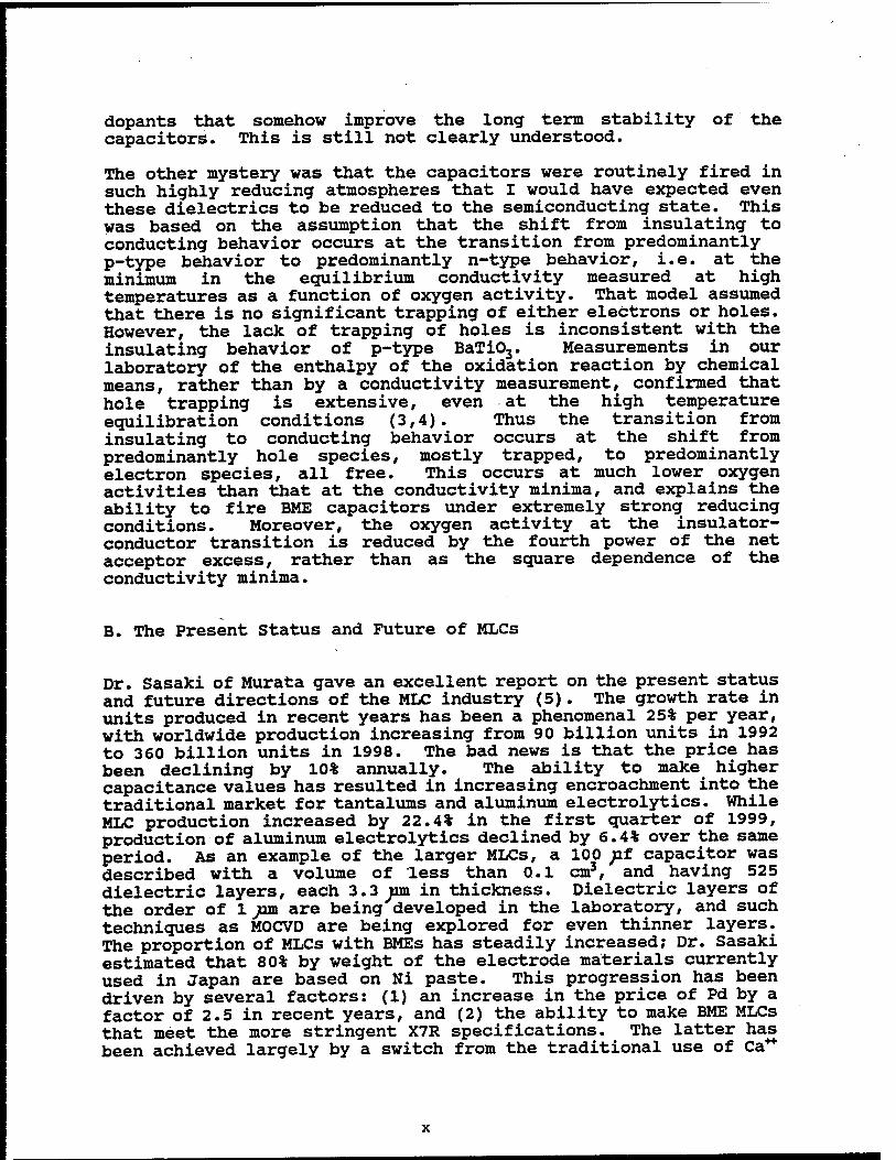
dopants that somehow improve the long term stability of the capacitors. This is still not clearly understood.
The other mystery was that the capacitors were routinely fired in such highly reducing atmospheres that I would have expected even these dielectrics to be reduced to the semiconducting state. This was based on the assumption that the shift from insulating to conducting behavior occurs at the transition from predominantly p-type behavior to predominantly n-type behavior, i.e. at the minimum in the equilibrium conductivity measured at high temperatures as a function of oxygen activity. That model assumed that there is no significant trapping of either electrons or holes. However, the lack of trapping of holes is inconsistent with the insulating behavior of p-type BaTi03. Measurements in our laboratory of the enthalpy of the oxidation reaction by chemical means, rather than by a conductivity measurement, confirmed that hole trapping is extensive, even at the high temperature equilibration conditions (3,4). Thus the transition from insulating to conducting behavior occurs at the shift from predominantly hole species, mostly trapped, to predominantly electron species, all free. This occurs at much lower oxygen activities than that at the conductivity minima, and explains the ability to fire BME capacitors under extremely strong reducing conditions. Moreover, the oxygen activity at the insulator- conductor transition is reduced by the fourth power of the net acceptor excess, rather than as the square dependence of the conductivity minima.
B. The Present Status and Future of MLCs
Dr. Sasaki of Murata gave an excellent report on the present status and future directions of the MLC industry (5). The growth rate in units produced in recent years has been a phenomenal 25% per year, with worldwide production increasing from 90 billion units in 1992 to 360 billion units in 1998. The bad news is that the price has been declining by 10% annually. The ability to make higher capacitance values has resulted in increasing encroachment into the traditional market for tantalums and aluminum electrolytics. While MLC production increased by 22.4% in the first quarter of 1999, production of aluminum electrolytics declined by 6.4% over the same period. As an example of the larger MLCs, a 100 ;tif capacitor was described with a volume of less than 0.1 cm3, and having 525 dielectric layers, each 3.3 jam in thickness. Dielectric layers of the order of 1 jam are being developed in the laboratory, and such techniques as MOCVD are being explored for even thinner layers. The proportion of MLCs with BMEs has steadily increased; Dr. Sasaki estimated that 80% by weight of the electrode materials currently used in Japan are based on Ni paste. This progression has been driven by several factors: (1) an increase in the price of Pd by a factor of 2.5 in recent years, and (2) the ability to make BME MLCs that meet the more stringent X7R specifications. The latter has been achieved largely by a switch from the traditional use of Ca**
X

as the acceptor dopant to rare earth cations, which will be discussed in the next section. L. A. Mann of Kernet described an alternative approach of using high Ag-low Pd electrodes with low- firing dielectric compositions (6). Dr. Mann estimated that at present material costs the break-even point between low-fired and BME capacitors lies at about 0.1 p.1, with BMEs being cheaper for higher values. If the price of Pd should return to its more traditional, lower values, the break-even point could shift to about 1 ^if.
C. The Use of Rare Earth Dopants for Capacitors with BMEs
In the last few years, there has been a shift in the doping of BME dielectric formulations from the traditional Ca-doping to the use of certain rare earths. Use of the latter dopants makes it possible to produce BME MLCs that satisfy the X7R and Y5V performance specifications, thus opening up a much wider market. This of particular interest to me because we worked out the site occupation preferences and resulting defect chemistry of rare earth doped BaTiO, some years ago. This was presented at the Orlando Meeting of the Electronics Division of the American Ceramic Society in 1985, and published in Advances in Ceramics in 1987 (7). In this study, the site preference as a function of ionic radius was determined directly by electrical measurement of the acceptor-donor behavior. The shape of the plot of the equilibrium conductivity data as a function of oxygen activity gives direct information on the balance of acceptor-donor behavior.
The rare earths represent a series of trivalent cations that gradually decrease in ionic radii with increasing atomic number as a result of the lanthanide contraction. If the rare earth substitutes for Ba** on the A-sites, it acts as a singly-charged donor, but if it substitutes for Ti*4 on the B-sites, it acts as a singly-charged acceptor. The experimental data can be superimposed on calculated plots for various site occupation ratios using published mobility data. We found that there is a gradual shift from A-site occupation for the larger ions, e.g. Nd+3 and Sm*3, to B-site occupation for the smaller ions, e^g. Yb*3. Cations of intermediate size, e.g. Er*3, divided themselves more evenly between the two sites, a behavior that has recently been called "amphoteric". This gradual, shift of site preference with ionic radius is at some variance with theoretical calculations by Lewis and Catlow that predicted that self-compensation would favor an equal division between the two sites to a much greater extent than observed (8).
It was also observed that the site occupation could be influenced by the Ba/Ti ratio, especially for the cations of intermediate size. Thus samples doped with Er*3 appear to be slightly donor doped in the presence of excess Ti, but almost purely acceptor doped in the presence of excess Ba. Clearly the presence of an excess for one site tended to drive the dopant to the other site.
XI
A subsequent paper focused on the behavior of Er*3 as a dopant, and describes the analysis of the equilibrium conductivity data in greater detail (9) . In this work it was found that Er*3 affected the Curie temperature and room temperature tetragonality only when it was forced onto the B-sites. It was shown quantitavely that Er*3
occupies only the B-sites in the presence of excess Ba. The solubility of Er*3 also appeared to be dependent on the Ba/Ti ratio. In an earlier study (10), the series Al*3, Sc*3, Y*3, and La*3, i.e. the Group III trivalent cations, were similarly studied and the results are mentioned in (7). Al*3 and Sc*3 were found to be B-site acceptors, La*3 an A-site donor, while Y*3 behaved very much like the amphoteric Er*3, which has an almost identical ionic radius.
The preceding discussion is a prelude to mention of the very nice review of rare earth doping given at the meeting by Randall in a plenary talk (11). This group studied the rare earth doped samples by XRD to obtain the unit cell volumes. It is gratifying that the behavior was just what would be predicted from our determination of site occupations, i.e. the larger cations go on the A-sites, the smaller cations go on the B-sites, and the cations of intermediate size go on both sites to varying degrees, and their choice can be affected by the Ba/Ti ratio. Similar conclusions were made by a group from Taiyo Yuden, based on both unit cell size and microstructural observations (12). There were some modest offsets between the findings of the three groups that can be attributed to different processing procedures.
Randall tried to quantify the site-selection process by using a site exchange reaction
R,.- + vTI"" < > v + v This implies that occupation of the B-sites creates barium vacancies, whereas it actually creates oxygen vacancies. It has never been shown that barium vacancies play any significant role in the defect chemistry of BaTiOj. Thus we have shown that in donor- doped compositions, even when formulated to contain the proper amount of compensating barium vacancies, the system rejects this opportunity and splits out sufficient Ti-rich second phase to leave compensating titanium vacancies (13). The ,reaction shown above, and the resulting mass-action treatment, thus seems to be incomplete. This group also found some effect on site occupation by variations in the oxygen activity, attributed to its effect on the oxygen vacancy concentration. For excess B-site occupation with acceptor-doped behavior, the effect should be small because the oxygen vacancy concentration is primarily fixed by the net acceptor content except under very strong reducing conditions. Even then the vacancy concentration varies only as the sixth root of the oxygen activity.
xii

D. Why Rare Earth Dopants?
Finally, it is not clear why the rare earth dopants are advantageous. If their role is to immobilize oxygen vacancies, one would expect Ca** to be even better. It is a doubly-charged center instead of singly-charged as are the rare earths, and it is larger than the amphoteric rare earths that are used in MLCs. Thus the rare earths have no advantage for either electrostatic or stress- related mechanisms of vacancy trapping. Secondly, why are the amphoteric rare earths most effective? As a first approximation this just introduces a mix of acceptor and donor centers, so why not just put in a mixture of a pure acceptor and a pure donor, e.g. a combination of Al+3 and La*3? Moreover, putting some of the dopant on the A-sites reduces the net acceptor content and hence reduces the movement of the insulating-semiconducting transition to lower oxygen activities, which was the purpose of the doping in the first place. The rare earths on A-sites are positive centers that are smaller than Ba*2 and would then repel oxygen vacancies for both electrostatic and elastic reasons. It has been suggested that the electronic structure of the rare earth ions is important for some reason presumably related to the partially filled 4f shells. Yet Y*3 also appears to be an effective dopant, and is amphoteric, but has the rare gas electronic structure of krypton and has no f electrons. Thus the peculiar effectiveness of the amphoteric trivalent dopants (certain rare earths and yttrium) in allowing the production of high quality MLCs with BMEs is not at all clear.
E. Summary
The development of dielectric compositions that can be fired under reducing conditions so that the expensive Ag-Pd electrodes can be replaced by Ni has been a prominent and interesting application of defect chemistry. This has kept the materials costs down so that these capacitors can effectively compete with alternative types. The improved properties that have been achieved by the replacement of the traditional Ca** dopant with the amphoteric rare earths have opened up an even wider market. While the basic behavior and site occupation choices for the rare earth dopants have been known for over 10 years, the reasons for the improved stability of capacitors with these newer dopants remains unclear.
F. References
1. Y. H. Han, J. B. Appleby, and D. M. Smyth, "Calcium as as Acceptor Impurity in BaTi03", J. Am. Ceram. Soc. 70., 96 (1987).
2. Y. Sakabe, T. Takagi, K. Wakino, and D. M. Smyth, "Dielectric Materials for Base-Metal Multilayer Ceramic Capacitors", Advances in Ceramics 19, 103 (1987).
Xlll

3. F. X. Ma, "Oxidation Enthalpy Measurements for Acceptor-Doped Perovskite Materials", M. S. Thesis, Lehigh University (1995).
4. M. V. Raymond and D. M. Smyth, "Defect Chemistry and Transport Properties of Pb(Zr1/2Ti1/2)03", Integrated Ferroelectrics 4, 145 (1994).
5. Y. Sakabe, "MLCs Technologies of Today and Future", 9th U.S.- Japan Seminar on Dielectric & Piezoelectric Ceramics", Nov. 2-5, Okinawa, Japan (1999).
6. L. A. Mann, "Advances in "Low-Fire" Dielectric Technology for the Manufacture of MLCC and Comparison with Base Metal Electrode Technology", U.S.-Japan Seminar on Dielectric & Piezoelectric Ceramics, Nov. 2-5, Okinawa, Japan, 281 (1999).
7. K. Takada, E. Chang, and D. M. Smyth, "Rare Earth Additions to BaTi03", Advances in Ceramics 12, 147 (1987).
8. G. V. Lewis and C. R. A. Catlow, J. Chem. Phys. Solids 42, 89 (1986).
9. K. Takada, J. Ichimura, and D. M. Smyth, "Equilibrium Conductivity for Er Doped BaTi03", Jap. J. of Appl. Physics 23., Supplement 26-2, 42 (1987).
10. R. Y.-F. Lee, "The Effect of A/B Ratio on the High Temperature Electrical Conductivity of Doped BaTi03 and SrTi03, M. S. Thesis, Lehigh University (1981).
11. C. Randall, Y. Tsur, and J. Van Tassel, "Scientific and Engineering Issues of the State-of-the-Art and Future Multilayer Capacitors", 9th U.S.-Japan Seminar on Dielectric & Piezoelectric Ceramics, Nov. 2-5, Okinawa, Japan, 7 (1999).
12. H. Kishi, N. Kohzu, and Y. Iguchi, "Occupational Sites of Rare Earth Elements in BaTi03", 9th U.S.-Japan Seminar on Dielectric & Piezoelectric Ceramics, Nov. 2-5, Okinawa, Japan, 311 (1999).
13. H. M. Chan, M. P. Harmer, and D. M.. Smyth, "Compensating Defects in Highly Donor-Doped BaTi03", J. Am. Ceram. Soc. 69, 507 (1986).
XIV

9 th Bi-annual US-Japan Seminar on Dielectric and
Piezoelectric Ceramics
Nov 3-5,1999
Okinawa, Japan
Jon-Paul Maria
North Carolina State University
Department of Materials Science and Engineering
Raleigh, NC 27695
In addition to the main conference in Okinawa, I visited Toshiba Corporation's Central Research
facility on October 29.
Visit to Toshiba Corporation's Central Research Facility
The visit to Toshiba was organized through Yoshiki Ishizuka, who worked as a visiting
scientist at North Carolina State University primarily in 1998. The official host for the Toshiba
visit was Dr. Noburu Fukushima. The work of Dr. Fukushima most closely mirrors that of our
group at NC State thus he was the most appropriate person.
xv
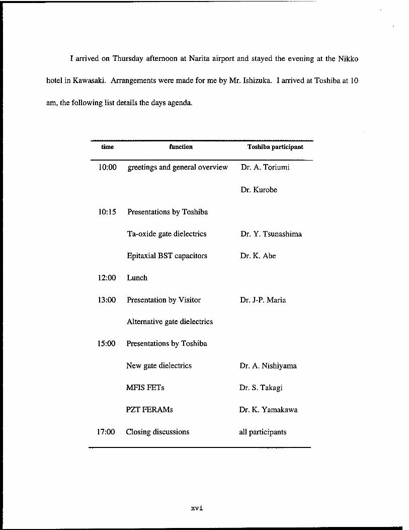
I arrived on Thursday afternoon at Narita airport and stayed the evening at the Nikko
hotel in Kawasaki. Arrangements were made for me by Mr. Ishizuka. I arrived at Toshiba at 10
am, the following list details the days agenda.
time function Toshiba participant
10:00 greetings and general overview Dr. A. Toriumi
10:15 Presentations by Toshiba
Dr. Kurobe
Ta-oxide gate dielectrics
Epitaxial BST capacitors
Dr. Y. Tsunashima
Dr. K. Abe
12:00 Lunch
13:00 Presentation by Visitor Dr. J-P. Maria
Alternative gate dielectrics
15:00 Presentations by Toshiba
New gate dielectrics
MFTSFETs
PZT FERAMs
17:00 Closing discussions
Dr. A. Nishiyama
Dr. S. Takagi
Dr. K. Yamakawa
all participants
XVI

My presentation at Toshiba focused on current research aimed at identification and
development of alternative gate dielectrics for silicon transistors. In addition, a general overview
of research in our group at NC State was presented. All materials were well received. Toshiba's
research and presentations on BST capacitors was particularly impressive. They appear to be
close to implementation of epitaxial capacitors in high permittivity embedded DRAM devices.
In the field of gate oxides, however, the Japanese community appears to be several years behind
the United States. Many Japanese researchers are still focusing on Ta^, a material which main
stream researchers in the US have largely abandoned for multiple reasons.
After the Toshiba presentations and discussions, Mr. Ishizuka acted as a host for the
entire evening and the next afternoon. Mr. Ishizuka paid for excellent dinners both Friday and
Saturday evenings and provided me with an excellent tour of the Tokyo area.
November 3rd - 5th tIS-.Tapan Seminar
• Traveled from Tokyo to Kyoto and met Professor David Cann of the Iowa State
University. Professor Cann and I spent a day touring Kyoto then traveled together from the
Kansai airport to Okinawa.
• Registered for the seminar on the evening of November 2 and attended the reception.
The meeting chairs, Dr. Shrout and Dr. Takenaka, did an excellent job making preparations. In
general, all social activities associated with the conference were organized similarly.
XVll

• Attended the seminar for the next three days, the following section discusses the
noteworthy presentations made in the general meeting.
Session I - Basic Science
• "MLC technologies of today and future" Yukio Sakabe, Murata Manufacturing Inc. Dr.
Sakabe gave an insightful presentation detailing the recent developments of Murata's capacitor
research. The specific topics of note were rare earth doping of MLCs with base metal electrodes
and thin film MLCs made by MOCVD. The thin film MLC work was rather impressive
especially in the context of the number of layers (15) and the remarkable smoothness of even the
top levels.
• "Ferroelectricity in SrTi(0I6018)" by M. Itoh. This talk was of great interest as it demonstrated
the ability to induce a ferroelectric phase transition in the normally incipient ferroelectric SrTi03
with the simple substitution of an oxygen isotope. Though no mechanistic details were
presented, the results were compelling.
Session II - Piezoelectric materials and devices
• "High piezoelectric performance in barium titanate single crystals with engineered domain
configurations", S. Wada. Professor Wada presented a delightful poster which discussed the
ability to engineer the domain configurations of ferroelectric materials when specific, and
xviii

unexpected, measurement orientations were used. Of particular interest was the ability to find
orientations where the dielectric loss and piezoelectric hysteresis values were exceptionally
small. Wada also suggested that this behavior could be true for all ferroelectric perovskites of
appropriate symmetry.
• "Fatigue anisotropy for rhombohedral PZN-PT single crystals", K. Takemura This work from
Penn State represents the latest breakthrough in the understanding of polarization fatigue for
ferroelectric materials. Takemura et al. found a specific orientation dependence to fatigue
suggesting an additional link to preferential domain switching.
Session III - Thin film dielectrics
• "The electrical properties of thin barium strontium titanate films and their impact on the
performance of capacitors for DRAM memories", T. Shaw. Dr. Shaw presented a discussion
detailing the recent developments for BST embedded DRAM memories. In depth discussions of
strain and composition effects were given which explained the possibilities and limitations for
DRAM based on paraelectric barium strontium titanate.
• "Synthesis of new pyrochlore compounds for transparent conductor applications", D. P. Cann.
Professor Cann prepared a poster discussing his recent efforts at producing new transparent
conducting oxides. Of particular interest to Dr. Cann is the ability to make a family of
XIX

transparent conductors whose band gap can be compositionally engineered. This work is of
technological importance for optical devices operating at increasingly short wavelengths.
Session IV - Multilayer ceramic capacitors
• "Dielectric property of BaTi03-BaZr03 solid solution under high electric field". T. Tsurumi.
Dr. Tsurumi's work investigated the high field behavior of the BTO-BZO system. Of particular
importance was the realization that the relaxor-like characteristics of such systems must be
considered when interpreting the high voltage characteristics. The ability to shift the
ferroelectric transition with field gives such materials a false voltage dependence of the dielectric
constant. This behavior must be well understood for reliable implementation into electronic
components, especially those targeted for high frequency or high power applications.
Summary
The 9th US-Japan seminar was of high technical quality and well managed. Organizers
from both sides did well to select an appropriate industrial and university cross section. The
conference participants represented a good mix of research topics currently of great scientific
interest, as well as those of industrial and economic importance. This was the second US-Japan
seminar that I attended. Once again, I have very positive reviews and intend to participate in
future years.
XX

9th U.S. Japan Seminar on Dielectric and Piezoelectric Ceramics
November 2-4 1999 Okinawa, Japan
David P. Cann Materials Science and Engineering
Iowa State University Ames, IA 50011
US-Japan Seminar on Dielectric and Piezoelectric Ceramics
I arrived in Okinawa on Tuesday afternoon on a flight from the new Osaka Kansai
airport. After registering for the meeting in the afternoon, I attended the reception which
was well attended. The following mornings session on basic science was highlighted by
the plenary lectures by Clive Randall and Yukio Sakabe. The rest of the morning session
consisted of talks concerning a number of topics including ferroelectricity, fatigue
resistance, and a number of talks on PZT. The most interesting talk came from M. Itoh
and R. Wang from the Tokyo Institute of Technology on the effects of I80 stoichiometry
in SrTi03. In their dielectric measurements they showed a strong relationship between
the maxima in permittivity and 180 content at cryogenic temperatures. The afternoon
session on piezoelectrics had a total of 26 presentations on various facets of piezoelectric
materials, devices, and applications.
xxx

The Thursday morning session on thin films was highlighted by a presentation by
Thomas Shaw of the IBM Microelectronics Division on thin film BST capacitors for
DRAM applications. Of the 22 other papers presented in this session a significant
fraction (11) was devoted to thin films of PZT. A total of four papers focused on
SrBijTajOg, 2 papers on PMN-PT, and the rest included pyrochlores, PbTi03, Bi4Ti3012,
and Ba(Sn,Mg,Ta)03. In this session I presented the recent results of our group on new
compounds with the pyrochlore structure which are aimed at transparent conducting
oxide applications. One of the more interesting talks was from H. Tamura et al of Murata
Manufacturing, on microwave measurements of HTSC electrodes on Ba(Mg,Sn,Ta)03
dielectric resonators. Large Q values for the dielectric resonators made with HTSC
electrodes were 7 times higher than Ag were recorded, but microstructural problems limit
the high frequency and high power applications.
Thursday afternoons presentations were focused on multilayer ceramic capacitors.
The plenary talk by Larry Mann of Kernet compared different multilayer capacitor
technologies. Using dielectric breakdown, mechanical strength, and life tests as a
comparison, he found that low-fire Ag-based and high-fire Ni-based capacitors showed
similar performance characteristics. Other talks in this session investigated the role of
rare-earth element doping in BaTi03 and the use of nano-sized powders in thick film
processing.
XXll

The conference ended with a session on advanced packaging and processing.
This session included discussions on chemical preparation routes for BaTi03,
(Pb,Ba)Nb206, and PZT among others.
I left immediately after the morning session flying back to Osaka, and then taking
the Shinkansen to the Tokyo-area. The weekend following the conference was spent
visiting with former Japanese colleagues including Dr. Koji Yamakawa of Toshiba, Mr.
Nakano Atsushi and Mr. Hitomi Atsushi of TDK Corporation, and Dr. Satoshi Wada of
the Tokyo Institute of Technology.
TDK Materials Research Center. Narita:
On the Sunday following the US-Japan meeting, I arrived in Narita with Mr.
Hitomi Atsushi and Mr. Nakano Atsuyuki of TDK. After spending the night in Narita,
the following morning I visited TDK's Materials Research Center facility. I gave an
informal presentation to the researchers from the ceramic R&D group including Takeshi
Takahashi and Dr. Christopher Williams (a visiting scientist from Cranfield). I presented
recent work on the following:
(i) pyrochlore oxides for transparent conducting coating applications
(ii) microelectrodes fabricated via focused ion beam (FEB) milling
XXlll

(iii) isotropic negative thermal expansion zirconium tungstate
I received valuable comments and suggestions from the audience on all three
topics. One idea that was borne out of our discussion was to look at the possibility of
ionic conduction in zirconium tungstate. Due to the open structure it is highly possible
that there are channels for conduction. There has been one report of possible oxygen
conduction in ZrW208. The interesting thing about ion conduction in ZrW208 is that
because of the negative thermal expansion the material may well have a negative thermal
coefficient of ionic conductivity unlike most other known ionic conductors.
After my presentation and the subsequent discussion I received a brief tour of
their facilities. Afterwards, TDK hosted a dinner at a local restaurant with Clive Randall
and Tom Shrout of Penn State who were visiting a different facility at the same time.
Mitsubishi Materials Central Research Institute. Omiya
On Tuesday morning the 9th of November I traveled to Omiya to visit Mitsubishi
Materials Central Research Institute. I was invited by Dr. Kuromitsu Yoshirou who was
a visiting scientist at the Materials Research Lab at Penn State while I was in graduate
school. Immediately following my arrival, Dr. Kuromitsu gave me a tour of their
XXIV

facilities. They have a wide range of expertise from powders, to magnetic materials, to
his current program on flat panel display technologies.
After having lunch with one of his coworkers Mr. Hideaki Sakurai I gave a
presentation on the same topic that I gave at TDK. The group was especially interested
in the transparent conducting oxide work due to their strong focus on display
technologies. After the meeting I spoke with members of the flat panel display group on
a variety of topics including wide band gap materials, low firing temperature conductors
using nanopowders, and suppression of secondary electron emission. Overall, I was
impressed with the quality of their processing technologies. With their current schemes,
they are able to get 100% yield on their 42 inch displays which use 0.2 mm cells. What
is most impressive is the number of layers in their device structure. Having such a high
yield over such a large surface is unlike anything else I know of in electronic ceramics.
Following my day at Mitsubishi Materials, I went to dinner with Dr. Kuromitsu and his
family.
The following day I returned to the US after a total of 9 full days in Japan.
Summary
In summary, I found the US-Japan meeting to be stimulating, very well organized
and was set in a beautiful setting in Okinawa. The conference organizer from Japan Dr.
XXV

Tadashi Takenaka in his opening remarks presented data illustrating of the increase in
size of the meeting over the years. I hope the meeting does not grow too large as I think
one of the most unique aspects of the meeting is the ease with which researchers can meet
and discuss their work in an informal relaxed atmosphere. This is the second US-Japan
meeting that I have attended and both have been amongst the best scientific conferences I
have attended.
The visits to TDK and Mitsubishi were also extremely insightful and well worth
the trip alone. In conclusion, I would like to thank the Office fo Naval Research for
sponsoring my trip.
xxvi

Travel-Report for the 9 US-Japan Seminar on Dielectric & Piezoelectric Ceramics
Herbert Giesche
NYSCC at Alfred University
General Comments
The organizer had chosen an appropriate location for that meeting. However, It would
have been nice to have some more social interaction. Besides the evening dinners there
was not too much possibilities to have a closer contact with some colleges. I have
attended two similar meetings/conferences in the past. They had been organized in a
slightly different way. Each day a general topic was given and after dinner the group
broke out into smaller discussion groups. After about 1 _ to 2 hours the groups came back
together and the results of each sub-group were presented to the entire group. The
interesting part of this exercise was the fact that a real discussion occurred instead of just
the presentation of research results. It also gave younger students (and faculty) the chance
to get a better feeling for the current research trends. Most people had been very free and
open to discuss not just what problems they have already solved but actually described
where they saw problems for which they did not have a ready answer or where the
research would be going in the next couple of years. The careful selection of leading
scientists in the respective areas and distributing them among the groups ensured that a
good balance was achieved. In my opinion those evening activities had a tremendous
effect on the overall success of the meeting. I would also recommend that the maximum
size for this kind of meeting should be 100 people or rather 80.
I was extremely impressed by the generous support and other contributions from several
of the Japanese companies.
XXVI1

Comments about the Scientific Program
The resent US-Japan seminar was the first meeting, which I attended in that scientific
area. I got only recently more involved in the area of electronic ceramic materials. I have
presently two projects that study the preparation of nanosized barium titanate powders by
a microemulsion synthesis technique. Thus, pretty much all talks and presentations were
new for myself. The meeting certainly helped me to gain a general understanding about
the present activities and seeing where there is a need for further improvements in this
area. I was especially interested in presentations, which focused on unique properties on
the basis of the chemical composition of the materials, since my own background is in
chemistry. Moreover, I was very interested in all kinds of powder synthesis techniques or
powder processing routes. From that point of view, especially the first session with the
plenary lectures by Yukio Sakabe and Clive Randall and also session V on advanced
processing and packaging had numerous highly interesting presentations.
From the large list of presentation I would highlight several of them, which were most
interesting for myself.
First there had been two presentations by Rayner and Whatmore, showing the application
of a piezoelectric device in a flextension motor as well as a traveling wave motor. Those
examples could certainly be extremely useful for any kind of miniaturized mechanical
devices or any device that would fall in the category of "lab on the chip". A second area
was the two plenary lectures by Thomas Shaw and Hidemi Takasu. Both of them focused
on the application in memory devices. The connection point to my own work was here
the scale down of device features into the nanometer size range. Any properties
influenced by the nanometer sized features can right away translated into properties
expected in nanosized powders. In session IV the plenary talk by LA. Mann was very
interesting since it provided again for myself a connection to nano sized materials. Mann
presented advances in low fire dielectric technology. The following poster session had
several interesting contributions. I would like to mention here only the presentation by
Gupta et al on chemically prepared barium titanate MLCC and the presentation by N.
XXVXll

Ogata et al on the development of nanosized silver metal platelets and the development of
an electrophoretic deposition process to form electrode layers in thin layered dielectrics.
The latter presentation was describing a very similar synthesis process, microemulsion
synthesis, as what I am presently using for the preparation of the barium titanate particles
and it also used electrophoretic deposition for the formation of layer structures. This is
very similar to plans in my own research project and I had a very fruitful discussion with
the author. I will most probably use this contact to develop a stronger interaction between
my own research group and the corresponding group at Perm State (Jim Adair & Clive
Randall).
Overall it was in some cases too much information for myself, which can certainly be
attributed to my own lack of knowledge, but the meeting helped to give me new ideas
and contact addresses for future cooperation. I am very interested to attend the next
meeting ofthat series and hope that at that time my own research has given me a much
better basis for a detailed discussions.
XXIX

ONR Trip Report:
The author attended the 9th US-Japan Seminar on Dielectric & Piezoelectric Ceramics from 2-5 November 1999 to and presented an invited talk.
While in Japan, he also visited on 8 November 1999 Taiyo Yuden Co. Ltd. in Gunma, a major producer of electroceramic components, where he was hosted by Dr. Masayuki Fujimoto. A second visit was made on 12 November 1999 to Panasonic's corporate research laboratories in Osaka, where a presentation was made on his piezoelectric research. Both of the companies visited expressed interest in developing lead-free substitutes for PZT and other lead oxide based dielectrics and piezoelectrics. Interestingly, the driving force for this was not considered to be new regulations in Japan, but in the European market into which both companies sell.
In between these 2 company visits, the author attended the Kyoto Prize Ceremonies in Kyoto, where W. David Kingery was honored as this year's laureate in Advanced Technology.
t-Ming Chiang November 11,1999
XXX

Participant List (U.S.)
Joanne Aller 169 Materials Research Lab. The Pennsylvania State University
University Park, PA 16802 USA Phone: 1-814-865-2896 Fax: 1-814-865-8126 e-mail: [email protected]
Ian Burn Director Research & Applied Technology Degussa-Huls 3900 South Clinton Av., South PlainfieldNJ 07080 USA Phone:31-908-226-2161
Fax: 31-908-757-0411 e-mail: [email protected]
Yet-Ming Chiang Room 13-4086, Dept. of Materials Science & Eng. Massachusetts Institute of Technology 77 Massachusetts Avenue, Cambridge, MA 02139 USA Phone: 1-617-253-5471 Fax: 1-17-253-6201 e-mail: [email protected]
Mike S.H. Chu Ferro Electronics Materials TAM Ceramics, Inc. 4511 Hyde Park Blvd., Niagara Falls, NY 14305 USA Phone: 1-716-278-9495 Fax: 1-716-278-9575 e-mail: [email protected]
Herbert Geische NYSCC at Alfred Univ.
2 Pine St., Alfred NY 14802 USA Phone: 1-607-871-2677 Fax: 1-606-871-2317 e-mail: [email protected]
Martin P. Harmer Materials Research Center Lehigh University Whitaker Lab, 5 East Packer Avenue Bethlehem, PA 18015 USA Phone: 1-610-758-4227 Fax: 1-610-758-3526 e-mail: [email protected]
David Cann Materials Science and Technology Iowa State University 3136 Gilman Ames, IA 50011 USA Phone: 1-515-294-3202 Fax: 1-515-294-5444 e-mail: [email protected]
L. Eric Cross 187 Materials Research Lab The Pennsylvania State University University Park, PA 16802 USA
Phone: 1-814-865-1181 Fax: 1-814-865-7846 e-mail: [email protected]
Rong-Fong Huang Electronic Material system Technology Motorola 7700 S. River Parkway, Tempe, AZ 85284 USA Phone: 1-480-755-6014 Fax: 1-480-755-5350 e-mail: [email protected]
Wenwu Cao 164 Materials Research Lab. The Pennsylvania State University
University Park, PA 16802 USA Phone: 1-814-865-4101 Fax: 1-814-865-2326 e-mail: [email protected]
Lynn Ewart Naval Undersea Warfare Center Code 2132, Bldg. 1170,1176 Howell Street, Newport RI02841- 1708 USA Phone: 1-401-832-5093 Fax: 1-401-832-6401
e-mail: [email protected]
Kerchner A. Jeffrey Cabot Corporation Boyertown PA 19512 USA Phone: 1-610-369-8268 Fax: 1-610-369-8552 e-mail: Jeff_Kerchner@cabot- corp.com
Jie Chen Imaging Systems Hewlett-Packard Company 3000 Minuteman Road, Andover, MA 01810 USA Phone: 1-978-659-2197 Fax: 1-978-687-7265 e-mail: [email protected]
Brian C. Foster Technical Manager Ferro Corporation 1709 Transelco Drive, Perm Yan, NY 14527 USA Phone: 1-315-536-3357 Fax: 1-315-536-0376 e-mail: [email protected]
Todd L Jessen US Naval Research Laboratory Code 6350,4555 Overlook avenue, SW Washington, DC 20375 USA Phone: 1-202-404-1534 Fax: 1-202-404-7176 e-mail: [email protected]
xxx x
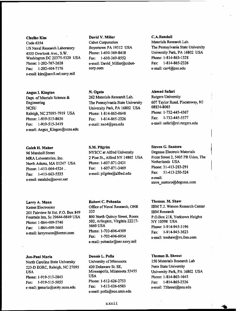
Chulho Kim Code 6354 US Naval Research Laboratory 4555 Overlook Ave., S.W. Washington DC 20375-5320 USA Phone: 1-202-767-2628 Fax: 1-202-404-7176 e-mail: [email protected]
David V. Miller Cabot Corporation BoyertownPA 19512 USA Phone: 1-610-369-8418 Fax: 1-610-369-8552 e-mail: David_Miller@cabot- corp.com
C.A.Randall Materials Research Lab. The Pennsylvania State University University Park, PA 16802 USA Phone: 1-814-863-1328 Fax: 1-814-865-2326 e-mail: [email protected]
Angus I. Kington Dept. of Mterials Science & Engineering
NCSU Raleigh, NC 27695-7919 USA
Phone: 1-919-515-8636 Fax: 1-919-515-3419 e-mail: [email protected]
N. Ogata 262 Materials Research Lab. The Pennsylvania State University University Park, PA 16802 USA Phone: 1-814-865-0648 Fax: 1-814-865-2326 e-mail: [email protected]
Ahmad Safari Rutgers University
607 Taylor Road, Piscataway, NJ 08854-8065 Phone: 1-732-445-4367 Fax: 1-732-445-5577 e-mail: [email protected]
Galeb H. Malier 96 Marshall Street MRA Laboratories, Inc. North Adams, MA 01247 USA Phone: 1-413-664-4524 . Fax: 1-413-663-5535 e-mail: [email protected]
S.M. Pilgrim NYSCC at Alfred University 2 Pine St., Alfred NY 14802 USA Phone: 1-607-871-2431 Fax: 1-607-871-3469 e-mail: [email protected]
Steven G. Santoro Degussa Electroic Materials Front Street 2, 5405 PB Uden, The Netherlands USA Phone:31-413-283-291 Fax: 31-413-250-524 e-mail: [email protected]
Larry A. Mann Kernet Electronics 201 Fairview St Ext. P.O. Box 849 Fountain Inn, Sc 29644-0849 USA Phone: 1-864-409-5746 Fax: 1-864-409-5665 e-mail: [email protected]
Robert C. Pohanka Office of Naval Research, ONR 332 800 North Quincy Street, Room 502, Arlington, Virginia 22217- 5660 USA Phone: 1-703-696-4309 Fax: 1-703-696-0934 e-mail: [email protected]
Thomas. M. Shaw IBM T.J. Watson Research Center IBM Research P.O.BOX 218, Yorktown Heights NY 10598 USA Phone: 1-914-945-3196 Fax: 1-914-945-3623 e-mail: [email protected]
Jon-Paul Maria North Carolina State University 223-D EGRC, Raleigh, NC 27695 USA Phone: 1-919-513-2843 Fax: 1-919-515-5055 e-mail: [email protected]
Dennis L. Polla University of Minnesota 420 Delaware St. SE, Minneapolis, Minnesota 55455 USA Phone: 1-612-626-2753 Fax: 1-612-626-6583 e-mail: [email protected]
Thomas R. Shrout 150 Materials Research Lab Perm State University University Park, PA 16802 USA Phone: 1-814-865-1645 Fax: 1-814-865-2326 e-mail: [email protected]
xxxii

Wallace Arden Smith Office of Naval Research, ONR 332 800 North Quincy Street, Room 502, Arlington, Virginia 22217- 5660 USA Phone: 1-703-696-0284 Fax: 1-703-696-0934 e-mail: [email protected]
S. Trolier-McKinstsry 151 Mateirals Research Lab. Penn State University University Park, PA 16802 USA Phone: 1-814-863-8348
Fax: 1-814-865-2326 e-mail: [email protected]
Donald M. Smyth Materials Research Center Lehigh University 5 E. Packer Ave. Bethlehem PA18015 USA Phone: 1-610-758-3852 Fax: 1-610-758-3526 e-mail: [email protected]
Dwight Viehland Naval Undersea Warfare Center, Code 2131 Bldg 1170, 1176 Howell Street, Newport, RI 02841-1708 USA Phone: l-800669-6892(x25107) Fax: 1-401-832-6401 e-mail: [email protected]
Tomohiro Sogabe Visiting Res., 161 Materials Research Lab. The Pennsylvania State University University Park, PA 16802 USA Phone: 1-814-863-3231 Fax: 1-814-865-2326 e-mail: [email protected]
Koto White Tokyo office US Air Force Office of Scientific Research 7-23-17 Roppoingi, Minato-ku Tokyo 106-0032 Japan Phone: 81-3-5410-4409 Fax: 81-3-5410-4407 e-mail: [email protected]
Stephen K. Streiffer MSD 212/C212, 9700 S. Cass Ave. Argonne National Laboratory Argonne, IL 60439-4838 USA Phone: 1-630-252-5832 Fax: 1-630-252-4289 e-mail: [email protected]
Hisao Yamada President Cerone, Inc. 2300 Overlook Road, #811, Cleveland Hts., OH #44106 USA Phone: 1-216-421-2248 Fax: e-mail: [email protected]
Koichi Takemura Functional Materials Research Laboratories NEC Corporation 4-1-1 Miyazaki, Miyamae-ku, Kawasaki 216-8555 Japan Phone: 81-44-856-2187
Fax: 81-44-856-2216 e-mail: [email protected]
Shoko Yoshikawa Director, Materials Research Active Control eXperts. Inc 215 First St. Cambridge, MA 02142 USA Phone: 1-617-577-0700 Fax: 1-617-577-0656 e-mail: [email protected]
xxxiii

XXXIV
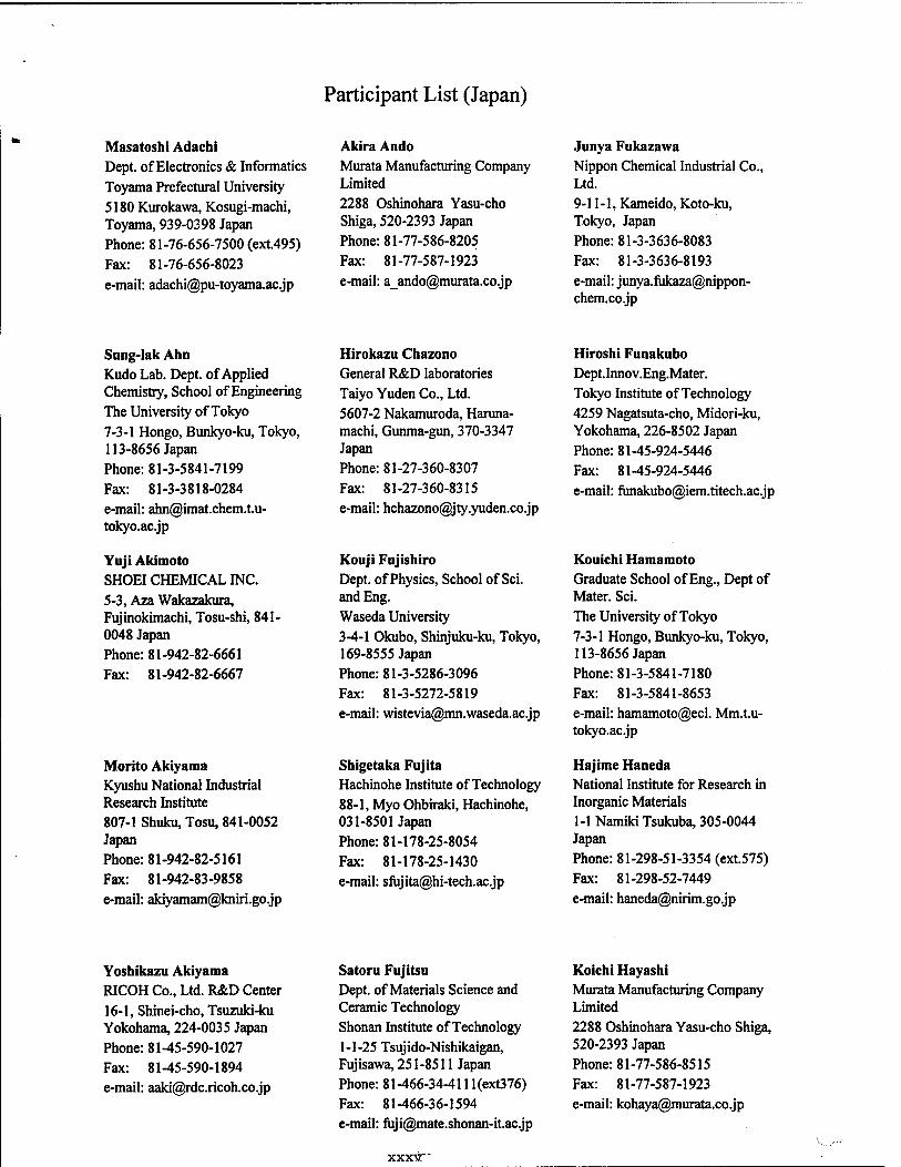
Participant List (Japan)
M asatoshi Adachi Dept. of Electronics & Informatics Toyama Prefectural University 5180 Kurokawa, Kosugi-machi, Toyama, 939-0398 Japan Phone: 81-76-656-7500 (ext.495) Fax: 81-76-656-8023 e-mail: [email protected]
Akira Ando Murata Manufacturing Company Limited 2288 Oshinohara Yasu-cho Shiga, 520-2393 Japan Phone: 81-77-586-8205 Fax: 81-77-587-1923 e-mail: [email protected]
Junya Fukazawa Nippon Chemical Industrial Co., Ltd. 9-11-1, Kameido, Koto-ku, Tokyo, Japan Phone: 81-3-3636-8083 Fax: 81-3-3636-8193 e-mail: junya.fukaza@nippon- chem.co.jp
Sung-lak Ahn Kudo Lab. Dept. of Applied Chemistry, School of Engineering The University of Tokyo 7-3-1 Hongo, Bunkyo-ku, Tokyo, 113-8656 Japan Phone: 81-3-5841-7199 Fax: 81-3-3818-0284 e-mail: [email protected] tokyo.ac.jp
Yuji Akimoto SHOEI CHEMICAL INC. 5-3, Aza Wakazakura, Fujinokimachi, Tosu-shi, 841- 0048 Japan Phone: 81-942-82-6661 Fax: 81-942-82-6667
Morito Akiyama Kyushu National Industrial Research Institute 807-1 Shuku, Tosu, 841-0052 Japan Phone: 81-942-82-5161 Fax: 81-942-83-9858 e-mail: [email protected]
Hirokazu Chazono General R&D laboratories Taiyo Yuden Co., Ltd. 5607-2 Nakamuroda, Haruna- machi, Gunma-gun, 370-3347 Japan Phone: 81-27-360-8307 Fax: 81-27-360-8315 e-mail: [email protected]
Kouji Fujishiro Dept. of Physics, School of Sei. and Eng. Waseda University 3-4-1 Okubo, Shinjuku-ku, Tokyo, 169-8555 Japan Phone: 81-3-5286-3096 Fax: 81-3-5272-5819 e-mail: [email protected]
Shigetaka Fujita Hachinohe Institute of Technology 88-1, Myo Ohbiraki, Hachinohe, 031-8501 Japan Phone: 81-178-25-8054 Fax: 81-178-25-1430 e-mail: [email protected]
Hiroshi Funakubo Dept.Innov.Eng.Mater. Tokyo Institute of Technology 4259 Nagatsuta-cho, Midori-ku, Yokohama, 226-8502 Japan Phone: 81-45-924-5446 Fax: 81-45-924-5446 e-mail: [email protected]
Kouichi Hamamoto Graduate School of Eng., Dept of Mater. Sei. The University of Tokyo 7-3-1 Hongo, Bunkyo-ku, Tokyo, 113-8656 Japan Phone: 81-3-5841-7180 Fax: 81-3-5841-8653 e-mail: hamamoto@ecl. Mm.tu- tokyo.ac.jp
Hajime Haneda National Institute for Research in Inorganic Materials 1-1 Namiki Tsukuba, 305-0044 Japan Phone: 81-298-51-3354 (ext.575) Fax: 81-298-52-7449 e-mail: [email protected]
Yoshikazu Akiyama RICOH Co., Ltd. R&D Center 16-1, Shinei-cho, Tsuzuki-ku Yokohama, 224-0035 Japan Phone: 81-45-590-1027 Fax: 81-45-590-1894 e-mail: [email protected]
Satoru Fujitsu Dept. of Materials Science and Ceramic Technology Shonan Institute of Technology 1-1-25 Tsujido-Nishikaigan, Fujisawa, 251 -8511 Japan Phone: 81-466-34-41 ll(ext376) Fax: 81-466-36-1594 e-mail: [email protected]
Koichi Hayashi Murata Manufacturing Company Limited 2288 Oshinohara Yasu-cho Shiga, 520-2393 Japan Phone: 81-77-586-8515 Fax: 81-77-587-1923 e-mail: [email protected]
XXXTT"

Takashi Hayashi Dept. of Materials Science and Ceramic Technology Shonan Institute of Technology 1-1-25 Tsujido-Nishikaigan, Fujisawa, 251-8511 Japan Phone: 81-466-34-41 ll(ext.370) Fax: 81-466-36-1594 e-mail: [email protected] it.ac.jp
Noboru Ichinose Waseda University 3-4-1 Ohkubo Shinjuku-ku Tokyo, 169-8555 Japan Phone: 81-3-5286-3307 Fax: 81-3-3200-2567 e-mail: [email protected]
Hiroshi Irie Research Center for Advanced Science and Technology The University of Tokyo 4-6-1, Komaba, Meguro-ku, Tokyo, 153-8904 Japan Phone: 81-3-5452-5300 Fax: 81-3-5452-5300 e-mail: [email protected] tokyo.ac.jp
Hiroshi Ishiwara Frontier Collabosrative Research Center Tokyo Institute of Technology 4259 Nagatsuda, Midoriku, Yokohama, 226-8503 Japan Phone: 81-45-924-5040 Fax: 81-45-924-5961 e-mail: [email protected]
Hiroyuki Kamei Suzuki Lab., Dept of Materials Science Shizuoka University 3-5-1 Johoku, Hamamatsu, 432- 8561 Japan Phone:81-53-478-1157 Fax: 81-53-478-1157 e-mail: [email protected]
Akinori Kan H. Ogawa Lab. Meijio University 1-501 Shiogamaguchi, Tenpaku- ku, Nagoya, 468-8502 Japan Phone: 81-52-832-1151(ext.5160) Fax: 81-52-832-1253 e-mail: [email protected]
Takashi Iijima Tohoku National Industrial Research Institute 4-2-1 Nigatake, Miyagino- ku, Sendai, 983-8551 Japan Phone:81-22-237-5211 Fax: 81-22-239-0629 e-mail: [email protected]
Toshiro Isoya Fuji Titanium Ind. Co.,Ltd,. 12-8 Sengen-Cho, Hiratsuka-City, 254-0041 Japan Phone: 81-463-32-1266 Fax: 81-463-32-1270 e-mail: [email protected]
Kazumi Kato National Industrial Research Institute of Nagoya 1 Hirate-cho, Kita-ku, Nagoya, 462-8510 Japan Phone:81-52-911-2179 Fax: 81-52-916-6992 e-mail: [email protected]
Hiroyuki Ikawa Dept of Applied Chemistry, Kanagawa Institute of Technology 1030 Shimo-ogino, Atsugi-shi, 243-0292 Japan Phone:81-462-91-3162 Fax: 81-462-42-8760 e-mail: [email protected]. kanagawa-it.ac.jp
Kenji Ito Degussa Japan Co., Ltd 2-3-1, Nishi-Shinjuku, Shinjuku- ku, Tokyo, 163-09 Japan Phone: 81-3-5323-7312 Fax: 81-3-5323-7396
Takeshi Kijima SHARP Corporation 273-1, Kashiwa, Kashiwa-shi, 277- 0005 Japan Phone:81-471-34-6116 Fax: 81-471-34-6119 e-mail: [email protected]
Akira Inaba Degussa Japan Co., Ltd 21 Kasuminosato, Ami-machi, Inashiki-gun Ibaraki, Japan Phone: 81-298-89-2801 Fax: 81-298-892804
Tsutomu Kajita R&D Dept.,Electric Material Div. Fuji Titanium Ind. Co.,Ltd,. 12-8 Sengen-Cho, Hiratsuka-City, 254-0041 Japan Phone: 81-463-32-1266 Fax: 81-463-32-1270 e-mail: [email protected]
Hiroshi Kishi General R&D laboratories Taiyo Yuden Co., Ltd. 5607-2 Nakamuroda, Haruna- machi, Gunma-gun, 370-3347 Japan Phone: 81-27-360-8307 Fax: 81-27-360-8315 e-mail: [email protected]
XXXVI

Radhika M.V. Rao Munekata Lab., Imaging Sei. & Eng. Lab. Tokyo Institute of Technology 4259 Nagatsuta-cho, Midori-ku, Yokohama, 226-8501 Japan Phone:81-45-924-5398 Fax: 81-45-924-5399 e-mail: [email protected]
Yukio Sakabe Murata Manufacturing Co., Ltd. 2288 Ooshinohara, Yasu-machi, Yasu-gun, 520-2393 Japan Phone: 81-77-586-8275 Fax: 81-77-587-1923 e-mail: [email protected]
Shigeki Sato Materials Research Center TDK Corporation 570-2 Matsugashita, Minamihatori, Narita-shi, 286- 8588 Japan Phone: 81-476-37-1637 Fax: 81-476-37-1648 e-mail: [email protected]
Tadashi Sekiya National Industrial Research Institute of Nagoya Hirate-cho, Kita-ku, Nagoya, 462- 8510 Japan Phone:81-52-911-2111 Fax: 81-52-916-6992 e-mail: [email protected]
Kiyoshi Shimamura Institute for Materials Research Tohoku University 2-1-1 Katahira, Aoba-ku, Sendai, 980-8577 Japan Phone:81-22-215-2103 Fax: 81-22-215-2104 e-mail: [email protected]
Kazuo Shinozaki Dept. of Metallurgy and Ceramic Science Tokyo Institute of Technology 2-12-1 Ookayama, Meguro-ku, Tokyo, 152-8552 Japan Phone: 81-3-5734-2518 Fax: 81-3-5734-3369 e-mail: [email protected]
Wataru Sakamoto Dept. of Applied Chem., Graduated School of Engineering Nagoya University Furo-cho, Chikusa-ku, Nagoya, 464-8603 Japan Phone:81-52-789-3345 Fax: 81-52-789-3182 e-mail: [email protected]
Kyoichi Sasaki Fuji Titanium Ind. Co.,Ltd,. 12-8 Sengen-Cho, Hiratsuka-City, 254-0041 Japan Phone: 81-463-32-1266 Fax: 81-463-32-1270
Takuji Seri The Rapid Progress of Organic Package Technology Kyocera Corporation 6 Takeda-Tobadono-cho, Fushimi- ku, Kyoto, 612-8501 Japan Phone: 81-995-46-8635 Fax: 81-995-46-8597
Yue Jin Shan Faculty of Engineering Utsunomiya University 7-1-2 Yoto, Utsunomiya, 321- 8585 Japan Phone: 81-28-689-6174 Fax: 81-28-689-6009 e-mail: [email protected] u.ac.jp
Tadashi Shiosaki Nara Institute of Science and Technology
8916-5 Takayama-cho, Ikoma, Nara, 630-0101 Japan Phone: 81-743-72-6063 Fax: 81-743-72-6069 e-mail: [email protected] nara.ac.jp
Hisao Suzuki Dept. of Materials Science Shizuoka University 3-5-1 Johoku, Hamamatsu, 432- 8561 Japan Phone:81-53-478-1157 Fax: 81-53-478-1157 e-mail: [email protected]
Motohiko Sato R&D Center NGK Spark Plug Co., Ltd. 2808, Iwasaki, Komaki, 485-8510 Japan Phone: 81-568-76-9704 Fax: 81-568-76-5274 e-mail: (y-okimura_rd@ mg.ngkntk.co.jp.)
Kenji Shibata Ya-man Ltd. Shingu Bldg. 4F, 2-4-2, Toyo Koto-ku, Tokyo, 135-0016 Japan Phone: 81-3-5635-1861 Fax: 81-3-5635-1866 e-mail: [email protected]
Sadayuki Takahashi R&D Group NEC Corporation 4-1-1, Miyazaki Miyamae, Kawasaki-shi, 216-8555 Japan Phone: 81-44-856-2164 Fax: 81-44-856-2128 e-mail: [email protected]
XXXV11

Yukichi Takamatsu Japan Pionics Co., Ltd 5181 Tamura, Hiratsuka-shi, 253- 0013 Japan Phone:81-463-53-8318 Fax: 81-463-53-8334
Takaaki Tsurumi Dept. of Inorg. Mater. Tokyo Institute of Technology 2-12-1 Ookayama, Meguro, Tokyo, 152-8552 Japan Phone: 81-3-5734-2517 Fax: 81-3-5734-2514
e-mail: [email protected]
Roger W. Whatmore TDK Nanotechnology Centere Cranfield University College Rd., Bedford, MK43 OAL, UK Phone: 44-1234-754057 Fax: 44-1235-751346
e-mail: [email protected]
Hidemi Takasu ROHM CO.LTD 21 Saiin Mizosakicho, Ukyo-ku, Kyoto, 615-8585 Japan Phone:81-75-311-2121 Fax: 81-75-321-6256 e-mail: [email protected]
Yoshiaki Uesu Dept. of Physics Waseda University 3-4-1 Okubo, Shinjuku-ku, Tokyo, 169-8555 Japan Phone: 81-3-5286-3446 Fax: 81-3-3202-4962 e-mail: [email protected]
Yasunori Yamaguchi Ya-man Ltd. Shingu Bldg. 4F, 2-4-2, Toyo Koto-ku, Tokyo, 135-0016 Japan
Phone: 81-3-5635-1861 Fax: 81-3-5635-1866
e-mail: [email protected]
Tadashi Takenaka Faculty of Sei. and Tech. Science University of Tokyo 2641 Yamazaki, Noda, 278-8510 Japan Phone: 81-471-24-1501(+3716)
Fax: 81-471-23-0856
e-mail: [email protected]
Satoshi Wada Dept. of Inorg. Mater. Tokyo Institute of Technology 2-12-1 Ookayama, Meguro, Tokyo, 152-8552 Japan Phone: 81-3-5734-2829 Fax: 81-3-5734-2514 e-mail: [email protected]
Takashi Yamamoto DeptElectrical Eng. National Defense Academy 1-10-20 Hashirimizu, Yokosuka, 239-8686 Japan Phone: 81-468-41-3810 (ext.2585) Fax: 81-468-44-5903 e-mail: [email protected]
Hiroshi Tamura Materials Production Dept. Murata Manufacturing Co., Ltd. Higashiokino, Yokaichi, Shiga, 527-8558 Japan Phone: 81-748-22-5500 Fax: 81-748-23-8009 e-mail: [email protected]
Masami Terasawa The Rapid Progress of Organic Package Technology Kyocera Corporation 6 Takeda-Tobadono-cho, Fushimi- ku, Kyoto, 612-8501 Japan Phone: 81-75-604-3500 Fax: 81-75-674-3411 e-mail: masami- [email protected]
Kikuo Wakino Honorary Corporate Advisor, Technology Murata Manufacturing Co, Ltd. 26-10, Tenjin 2-chome, Nagaokakyo-shi, Kyoto, 617-8555 Japan Phone: 81-75-955-6504 Fax: 81-75-958-2219
e-mail:
Ruiping Wang Materials and Structure Lab. Tokyo Institute of Tecnology 4259 Nagatsuta, Midori-ku, Yokohama, 226-8503 Japan Phone: 81-45-924-5626 Fax: 81-45-924-5626 e-mail: [email protected]
xxxviii
Yohachi Yamashita Research & Development Center, [PML] Toshiba Corp. 1 Komukai Toshiba-Cho, Kawasaki, 210-8585 Japan Phone:81-44-549-2118 Fax: 81-44-520-1286 e-mail: yohachi.yamashita@ toshiba.co.jp

9TH US-JAPAN SEMINAR ON
DIELECTRIC AND PIEZOELECTRIC CERAMICS
November 2-5,1999 Okinawa, Japan
PROGRAM
TUESDAY, NOVEMBER 2
18:00 Registration and Welcome Reception
WEDNESDAY, NOVEMBER 3
8:45-9:00 Opening Remarks: T. Takenaka (Science University of Tokyo, Japan)
Session I—Basic Science
Session Chair: Susan Trolier-McKinstry, The Pennsylvania State University Takashi Yamamoto, National Defense Academy
9:00-10:00 Plenary Lectures page
PI-1 MLCs Technologies of Today and Future, Yukin Sakahp Murata 1 Manufucturing Co., Ltd., Japan
PI-2 Scientific and Engineering Issues of the State-of-the-Art and Future 7 Multilayer Capacitors, Clive Randall Y. Tsur and J. Van Tassel, The Pennsylvania State University, USA.
10:00-10:30 Break
10:30-11:20 Contributed Papers
1-1 Phenomenology of the Elasto-Dielectric Response in the Field Forced 15 Ferroelectric Phases of Lead Zinc Niobate: Lead Titanate (PZN : PT) Relaxor Ferroelectrics, L. Eric Cms* and Petr Hana, The Pennsylvania State University, USA.
1-2 Domain Structure of PbTi03 Single Crystals by Kelvin Force Microscope, 19 Takashi Yamamoto, Shinobu Omika, Junichi Sakamoto and Eiji Matsuzaki National Defense Academy, Japan
1-3 SHG Microscope: Principle and Its Application to Nondestructive Observation 23 of 180°, Domain Structure and Domain Reversal Process in Ferroelectrics, Haruyuki Mohri, Sunao Kurimura and Ynshiaki Tb.su Department of Physics, Waseda University, Japan
1-4 (Ba,Sr)Ti03 Dielectrics: Relationship between Bulk and Thin Film Properties, 27 Angus I. Kingon and Charles B. Parker, Dept. of Materials Science and Engineering, North Carolina State University; Stephen K. Streiffer, Argonne National Laboratories; and Susanne Stemmer, University of Illinois, USA
XXXIX

1-5 Quantum Paraelectricity in Epitaxial Titanate Perovskites, R.M.V.Rnn 31 KShimada, M.Lippmaa, M.Kawasaki, Y.Inaguma, MJtoh, H.Munekata and H. Koinuma, Tokyo Institute of Technology, Japan
1-6 Charge Transport and Fatigue Resistance in SrBiJaA, A.C. Palanduz, 35 Massachusetts Institute of Technology and Donald M. Smyth Lehigh University, USA.
1-7 Structure and Ferroelectric Properties of Bismuth-Layer-Structured 39 Ferroelectric Single Crystals, Hiroshi Me. Masaru Miyayama and Tetsuichi Kudo, The University of Tokyo, Japan
1-8 Commonalities of the Influence of Lower Valent Substitutents on PZT, 43 Dwight Viehland. Naval Sea Command, USA
1-9 Domain Switching and Rotation in Soft and Hard PZT Ceramics, Toxhin 47 Ogawa. Shizuoka Institute of Science and Technology, Japan
I-10 Ferroelectricity-Evoking Mass-Inequality Factor for Perovskite Titanates 51 ATi03, Tetsuro Nakamura, Yue Jin Shan, Utsunomiya University; Mitsuru Itoh and Yoshiyuki Inaguma, Tokyo Institute of Technology, Japan
I-11 Dielectric Properties and Depoling Characteristics of PB(Zr005Ti00J)O, Based 55 Ceramics: Near-Critical Grain Size Behavior, B.A. Tuttle. JA. Voigt, T.W. Scoßeld, P. Yang, D.H. Zeuch, and M.A. Rodriguez, Sandia National Laboratories, USA
1-12 Ferroelectricity in SrTi(160,.xll!Ox)3, Mitsuru Itoh and Ruiping Wang Tokyo 59
Institute of Technology, Japan
1-13 Diffusion of Oxide Ions in Zinc Oxide Ceramics and Thin Films, Hajime 63 Hamda, Isao Sakaguchi, Akio Watanahe, Manabu Komatsu, , *Tsuyoshi Ogino ,**Tadashi Takenaka and ***Naoki Ohashi, NIRIM, *Kyushu Univ. **Sci. Univ. of Tokyo, ***Tokyo Institute of Technology, Japan
11:20-12:30 Poster View
12:30-14:00 Lunch
Session II —Piezoelectric Materials and Devices
Session Chair: Ahmad Safari, Rutgers University Akira Ando, Murata Manufacturing Co., Ltd.
14:00-15:00 Plenary Lectures . Page
PH-1 Advance Processing Technology for Piezoelectric Ceramics, Kazuo Miyahe. 67 Kazushi Tachimoto, Kenji Horino, Masakazu Hirose, Mahoko Takada, Takeo Tsukada, Tomohisa Azuma and Junichi Yamazaki, TDK Corporation, Japan
PII-2 Lead Free High Actuation Strain Single Crystal Piezoelectrics and Fibers, i&t 75 Ming Chiang, G. W. Farrey, A.N. Soukhojakk and S.A. Sheets, Massachusetts Institute of Technology, USA
xxxx

15:00-16:30 Contributed Papers
n-1 High Piezoelectric Performance of Barium Titanate Single Crystals with 83 Engineered Domain Configurations, Satoshi Wnda Shingo Suzuki, Tatsuo Noma, Takeyuki Suzuki, Minoru Osada, Masato Kakihana, Tokyo University of Agriculture & Technology, Japan; Seung-Eek Park, L. Eric Cross and Thomas R. Shrout, Penn State University, USA
n-2 Crystallographicaily Engineered Single Crystals for High Performance 87 ?vzzoe\QC\ncs, Seung-Eek Park, Satoshi Wada* Paul Rehrig, Shi-Fang Liu L Eric Cross, and Thomas R. Shrout, The Pennsylvania State University, USA- *Tokyo University of Agriculture and Technology, Japan.
n -3 Non-180° Domain Contribution to the Properties of PZN-PT Single Crystals 91 Takaaki Tsurumi, Keishiro Okamoto, Naoki Ohashi, Tokyo Institute of Technology; and Yohachi Yamashita, Toshiba corp., Japan
II -4 Effective Material Properties of a Multi-domain Ferroelectric Material, Wenwu 95 Caa andJif i Erhart, The Pennsylvania State University, USA.
n-5 Fatigue Anisotropy for Rhombohedral Pb(Zn1/3Nb2/3)03-PbTi03 Single 99 Crystals, Kokhi Takemura*, Metin Ozgul, Veronique Bornand, Susan Trolier- McKinstry, and Clive A. Randall, The Pennsylvania State University, USA; *NEC Corporation, Japan.
n-6 Relaxor-Based Single Crystals by Seeded Polycrystal Conversion, Martin P 103 Harmer, Helen M. Chan, Ajmal Khan, Tao Li, Suxing Wu, Adam M. Scotch, Lehigh University, USA.
n-7 The Growth of PMN-PT Single Crystals by the Solid State Method, Hhaa 107 Yamada, Cerone, Inc., USA
n-8 Crystal Growth and Characterization of New Langasite-type Compounds for 111 Piezoelectric Applications, Kivoshi Shimamum Tomohiko Kalo, Jun Sato and Tsuguo Fukuda, Tohoku University, Japan
II-9 Crystalline Structure and Piezoelectric Properties of Bi Layer Structured 115 Compound SrBi2Nb209, Akira Ando, Masahiko Kimura and Yukio Sakabe, Murata Manufacturing Company Limited, Japan
n-10 The Thickness-Extensional and Thickness-Shear Vibration Mode 119 Characteristics of Bismuth Layer-Structure Compounds, Hitoxhi Okn Masakazu Hirose, Takeo Tsukada, Keisuke Itakura and Yasuharu Mjiyauchi, TDK Corporation, Japan
n-11 Additive Effects on Piezoelectric Properties of (Bi1/2Na1/2)Ti03 Ceramics, 123 Hajime Nagata, Sinichi Morita, Akihiro Itoh and Tadashi Takenaka, Science University of Tokyo, Japan
n-12 Processing and Piezoelectric Properties of Pb(NiI/3Nb2/3)03-PbTi03-PbZr03 127 Solid Solutions from PbO-excess Compositions, Keiii Kusvmntn and Tadashi Sekiya, National Industrial Research Institute ofNagoya, Japan
n-13 Properties of PMN and PZT in Compression, Lvnn Ewart Elizabeth A. 131 McLaughlin, and Kim Gittings, Naval Undersea Warfare Center, USA
XXXXl

n-14 High Frequency Piezoelectric Properties of Lead Titanate, Koichi Hnvgshi 135 Akira Ando and Yukio Sakabe, Murata Manufacturing Company Limited, Japan
II -15 Composites and Medical Imaging Arrays for Frequencies Above 20 MHz, T.A. 139 Ritter, K.K. Shung, R.L. Tutwiler, and T.R. Shmut. The Pennsylvania State University, USA
n-16 Single Crystal Transducers for Medical Imaging Applications, R.K. Panda, 143 J.Chen. H. Beck and T.R. Gururaja, Imaging Systems, HewlettPackard Co., USA.
11-17 Piezoelectric Ultrasonic Motor using Flextensional Amplification of a Disc 147 Radial Mode with Elastic Fin Drive, Philip J. Rayner and Roger W. Whatmore. TDK Nanotechnology Centre, Cranfield University, UK
II-18 Travelling Wave Ultrasonic Motor using the Bog Flexural Mode of a Circular 151 Membrane, Philip J. Rayner and Roger W. Whatmore. TDK Nanotechnology Centre, Cranfield University, UK
n-19 Piezoelectric Actuators and Dampers Using Interdigital Electrodes, Shoko. 155 Yoshikawa. Michael Farrell, David Warkentin, Robert Jacques, and Erik Saarmaa, ACX, Inc., USA.
11-20 Dielectric Studies of K(TaxNb,.Jt)03 and Pb(Fe2/3WI/3) for Use as Ferroic 159 Materials at Cryogenic Temperatures, C.B. DiAntonio and S.M. Pilgrim. New York State College of Ceramics at Alfred University, USA
n-21 The Development of Piezoelectric Ceramic Torsional Actuators Based on 163 Shear Piezoelectric Response and Their Potential Applications, Chulho Kim. Naval Research Laboratory, USA; Aglexandre Glazounov, Universität Karlsruhe, Germany; and Qiming Zhang, The Pennsylvania State University, USA.
n-22 Development of Pb(Zr,Ti)03-based Ceramics for Photostrictors, Kazuhiro 167 Nonaka. Morito Akiyama, Tsuyoshi Hagio and Akira Takase, Kyushu National Industrial Research Institute, Japan
II-23 The Dynamic Analysis of Kyser-type Ink-Jet Head, Yujiro Kitaide, Fuji 111 Electric corporate R&D, Ltd, Japan
n-24 Study of Electric-Field-Induced Strain in PLZT, Yoshikazu Akiyama. Ricoh 175 Co., Ltd. R&D Center, Japan
16:30-18:00 Poster View, Discussion and Break
XXXX11

THURSDAY, NOVEMBER 4
Session III—Thin Film Dielectrics
Session Chair: Angus Kingon, North Carolina State University Tadashi Shiosaki, Nara Institute of Science and Technology
8:30-9:30 Plenary Lectures Page
Pm-1 The Electrical Properties of Thin Barium Strontium Titanate Films and their 179 Impact on the Performance of Capacitors for DRAM Memories, Thomas Shaw*, J.D. Banieckf, R.B. Laibowitz* E. Liniger* Z. Suon, M. Huang* D.E. Kotecki**, J. Liann, H. ShentT; *IBM Research Division, **IBM Microelectronics Division, 'Columbia University, TTPrinceton University, "Siemens Microelectronics Inc., USA.
Pm-2 The Ferroelectric Memory Technology and Its Application, Hidemi Tnkn<n, 185 Rohm Co. Ltd, Japan
9:30-11:00 Contributed papers
m-1 Orientation Mechanism and Electrical Properties of Low-Temperature 191 Processed Sol-Gel Derived PZT Thin Film, Hisan Swuld Yasuhiro Kondo, Shoji Kaneko, Shizuoka University; and Takashi Hayashi, Shonan Institute of Technology, Japan
m-2 A Wet-Oxidation Process for Sputter-deposited Pb(Zr, Ti)03 Films, Sonp-Min 195 Mam, Hiroyuki Kimura, Naoki Ohashi and Takaaki Tsurumi, Tokyo Institute of Technology, Japan
m-3 Electric Conduction Characteristics of Pb(Zr, Ti)0, Thin Films Measured with 199 Interdigitated Electrodes, Hirntake Okinn Toshihisa Horiuchi, Hirofumi Yamada and Kazumi Matsushige, Kyoto University, Japan
KI-4 Microstructures of Sol-Gel Derived PZT Thin Films, Kazunari Maki 203 Nobuyuki Soyama, Satoru Mori, Kensuke Kageyama, Masaya Matsuura and Katsumi Ogi, Mitsubishi Materials Corporation, Japan
m-5 Effects of Stacking Structure on Crystallization and Electrical Properties of 207 Pb(Zr0j3Ti047)O3 Thin Films from Stable Precursor Sol, Hisao Suzuki and Takahiro Koizumi. Shizuoka University, Japan
m-6 Effects of B-site Substitution in Ferroelectric PbTi03 Thin Films on Crystal 211 Structure and Electrical Properties, Masato Mivake Akihisa Inoue, Ryo Teraura, Takashi Nishida, Soichiro Okamura and Tadashi Shiosaki, Nara Institute of Science and Technology, Japan
m-1 Texture Control of Sol-Gel Derived PZT Thin Films, Takashi I[nmn 215 Toshihiko Abe and Norio Sanada, Tohoku National Industrial Research Institute, Japan
m-8 Optimization of Buffer Layers and Device Structures in Ferroelectric-Gate 219 FETs, Hiroshi Ishiwara, Eisuke Tokumitsu and Gen Fuj'ii, Tokyo Institute of Technology, Japan
XXXXlll

m-9 Pb(Mg1/3Nb2/3)03-PbTi03 Thin Films Synthesized by Metalorganic Chemical 223 Vapor Deposition, Stephen K. Streiffer.G.R. Bai, O. Auciello, P.K. Bauman, K. Ghosh, and A. Mukholm, Argonne National Laboratory; C. Thompson, Northern Illinois University and Argonne National Laboratory; S. Stemmer, University of Illinois at Chicago; and R.A. Rao and C.-B. Eom, Duke University; USA
m-10 Dielectric Behavior of Multilayered Pb(Mg,/3Nb2/3)03-PbTi03 Thin Film by 227 Chemical Solution Deposition, Hisao Suzuki, Hiroyuki Kamei. Shizuoka University; Masami Kishi, Hokkaido Institute of Technology; Junichi Takahashi and Kohei Kodaira, Hokkaido University, Japan
IH-11 Piezoelectric Measurement of Thin Film Ferroelectric using AFM with an 231 RT6000, Kenji Shibata. Yasunori Yamaguchi,Yarman Ltd.; Joe T. Evans Jr., Radiant Technologies Inc.; Seigen Otani, Fujitsu Laboratories Ltd.; and Masatoshi Yasutake, Seiko Instruments Inc. Japan
M-12 Measurement and Calculation of PZT Thin Film Longitudinal Piezoelectric 235 Coefficients, Hiroshi Maiwa. Jon-Paul Maria*, James A. Christman* Seung-Hyun Kim*, Stephen K Slreiffer** and Angus I. Kingon* Shonan Institute of Technology, Japan, *North Carolina State University, USA, **Argonne National Laboratory, USA
IH-13 Application of Piezoelectric MEMS in Biomedical Engineering, Dennis L. 239 Polla. William P. Robbins, University of Minnesota, USA
IE-14 Growth of Epitaxial Bi-layered Ferroelectric Thin Films by MOCVD and 243 Their Electrical Properties, Hiroshi Funakuho. Katsuyuki Ishikawa, Takayuki Watanabe andNorimasa Nukaga, Tokyo Institute of Technology, Japan
IH-15 Low-Temperature Processing Using Complex Alkoxides for Ferroelectric 247 SrBi2Ta209 Thin Films, Kazumi Koto. National Industrial Research Institute ofNagoya, Japan
m-16 Ferroelectric Properties of Bismuth Layer-Structured SrmJ+JBi4.xTim.xTaxOJ/7+i 251 (m=2, x=l-2; /w=3, x=Q-2), Tadashi Takenaka. Hajime Nagata, Naohito Chikushi and Takeshi Takahashi, Science University of Tokyo, Japan
111-17 Structural Analyses of Ferroelectric SrBi2Ta209 Thin Films Prepared by Sol- 255 Gel Method, Ichiro Koiwa. Hiroyo Kobayashi, Keiji Tatani, Oki Electric Industry Co., Ltd. Japan; Kazuya Sano, The Japan Steef Works, Ltd.; Akira Hashimoto, Yoshihiro Sawada, Tokyo Ohka Kogyo Co., Ltd.; and Tetsuya Osaka, Waseda University, Japan
ni-18 Orientation Control of Bi4Ti30,2 Thin Films by MOCVD, Takeshi Kjiima. 259 Yutaka Nagawasa andKaoru Suzuki, SHARP Corporation, Japan
m-19 Bismuth Pyrochlore Films for Dielectric Applications, W. Ren, R. Thayer, C.A. 263 Randall, andS. Tralier-McKinstrv. The Pennsylvania State University, USA
IE-20 Microwave Properties of High-Tc Superconducting Thick Films on 269 Ba(Sn,Mg,Ta)03 Dielectric Resonator and Silver Plate, Hiroshi Tamura. Tsutomu Tatekawa, Yuji Kintaka, Murata Manufacturing Company Limited, ; andAkio Oota, Toyohashi University of Technology, Japan
xxxxiv

m-21 Synthesis of New Pyrochlore Compounds for Transparent Conductor ->73 Applications, Ravindran Mohanavelu, Alan P. Constant, and David P Can» Iowa State University, USA r nm
m-22 Ferroelectric Domain Pinning in PZT Thin Film Deposited on Pt and Oxide 277 Buffer Electrodes, Yokhiro Masuda Shigetaka Fujita, Hachinohe Institute of Technology; ,and Takashi Nishida, Nara Institue of Science and Technology Japan a"
11:00-12:30 Poster View, Discussion and Break
12:30-14:00 Lunch
Session IV—Multilayer Ceramic Capacitors
Session Chair: Donald M. Smyth, Lehigh University Hirosi Kishi, Taiyo Yuden Co., Ltd.
14:00-15:00 Plenary Lectures Page
PIV-1 Advances in "Low-Fire" Dielectric Technology for the Manufacture of MLCC 281 and Comparison with Base Metal Electrode Technology, I.A. Mann Kernet Electronics Corp., USA
PIV-2 Research Trends of Relaxor Ferroelecric Materials in Japan, Nohoru Trhinn^ 289 Waseda University, Japan
15:00-16:30 Contributed papers
IV-1 Binder Burn-out Process for Highly Reliable MLCCs with Ni Electrodes, 295 Takeshi Nomura, Tamami Kato and Yukie Nakano, TDK Corp., Japan
IV-2 Ni Compatible X7R and Y5V Dielectrics: The Evolution in Technology, L 299 Bum, D. Lee, D. Spang, and D. Swanson, Degussa Hüls, USA; W. Derks]J. Roelofsma, andS. Santoro, Degussa-Hüls, The Netherlands.
1V-3 Influence of the Microstructure on the Redox Behavior in BTZ Based 303 Material, Hirokazu Chazann. Yasuyuki Inomata, Noriyuki Kohzu, and Hiroshi Kishi, Taiyo Yuden Co., Ltd., Japan
IV-4 A New BaTi03 for Low Fire Y5V and BME Y5V Dielectrics, S. Butcher, M. 307 Chit, V. Ganine, D. Rose, and T. Stone, TAM Ceramics, Inc., USA.
IV-5 Occupational Sites of Rare-Earth Elements in BaTi03, Hiroshi Kishi, Noriyuki 311 Kohzu, Yoshiaki Iguchi, Taiyo Yuden Co., Ltd.; Junichi Sugino, Hitoshi Ohsato and Takashi Okuda, Nagoya Institute of Technology, Japan
IV-6 Effect of Rare-Earth Doping on the Temperature-Capacitance Characteristics 315 for MLCCs with Ni Electrodes, Shigeki Sato Yoshinori Fujikawa, Akiko Nagai, Yoshihiro Terada, and Takeshi Nomura, TDK Corp. Japan
xxxxv

rV-7 Aqueous-Based, Ni-Electrode Compatible Dielectrics for Advanced MLCC 319 Applications, Sridhar Ve.nwalla. David V. Miller, Jefferey A. Kerchner, Kathleen A. Thrush, and Stephen A. Costantino, Cabot Corp., USA.
IV-8 Effect of Multiplication on Residual Stress and Reliability of MLCCs with Ni- 323 electrode, Yukie Nakano. Takeshi Masuda and Takeshi Nomura TDK Corp. Japan
IV-9 A Low Dielectric Aging X7R BaTi03 Ceramic for BME MLC, Yohachi 327 Yamashita. Toshiba Corp.; Nakano, H. Shoji, KHanda and H. Ogawa, Nippon-Chemi-Con Co., Ltd., Japan
IV-10 Use of Chemically Prepared BaTiCO in the Manufacturing of Multilayer 331 Ceramic Capacitors, S.P. Gupta, Tom Poole and Jeff Franklin, Kernet Electronics Corp., USA.
IV-11 Development of Nanosize Particles for Thin Layer Dielectrics, D.O. Yener, K. 335 Ogata.C.A. Randall, andJ.H. Adair, Penn State University, USA.
IV-12 Nanostructured Barium Titanate Prepared in Microemulsions, Herbert 339 Geische. New York State College of Ceramics at Alfred University, USA.
IV-13 Development of Ultra-Low Fire COG and X7R Dielectric Compositions for 341 Integrated Passive Component Applications, Brian C. Foster. Walter J. Symes, Everette A. Davis, and Matthew J Creedon, Ferro Corporation, USA
IV-14 Dielectric Property of BaTi03-BaZr03 Solid Solution under High Electric 345 Field, Takaaki Tsurumi. Yuichi Yamamoto, Naoki Ohashi, Tokyo Institute of Technology; Hirokazu Chazono, Yasuyuki Inomata and Hiroshi Kishi, Taiyo Yuden Co.,Ltd., Japan
IV-15 Dielectric Development for High Voltage Filter Capacitor Applications, Z. 349 Jesssm, M. Chase, L. Kurihara, and M. Kahn, Naval Research Laboratory, USA
IV-16 Dielectric Properties of MnO-Doped BaTi03 for Ni Electrode MLCCs, 353 Takeshi Masuda. Akira Yamamoto and Takeshi Nomura, TDK Corp., Japan
IV-17 Highly Accelerated Life Testing (HALT) of K-4500 Low Fired X7R 357 Dielectric, Galeb H. Mäher. MRA Laboratories, Inc., USA.
IV-18 Crystal Structure and Dielectric Properties of Perovskite Oxides 363 A(Sc1/2MI/2)03 (A =Ca, Sr, M = Nb, Ta), Ayukn Ozeki. Yue Jin Shan, Tetsuro Nakamura Utsunomiya University; and Mitsuru Itoh, Tokyo Institute of Technology, Japan
IV-19 The Quality Factor of the Ba^R^Ti^ (R = Rare Earth) Solid Solutions 367 Depended on the Ionic Size Difference Between Ba and R, Hitoshi Ohsato. Masaki Imaeda, *Hideyasu Sakashita andSusumu Nishigaki, Nagoya Institute, of Technology, *Daiken Chemical Co., Ltd., Japan
IV-20 Effects of Alkali Metal Oxide Addition on the Microwave Dielectric 371 Properties of the BaO-Sm203-Ti02 Ceramics, Motohika Satn. Jun Otsuka, Hitoshi Yokoi and Kazushige Ohbayashi, NGK Spark Plug Co., Ltd., Japan
xxxxvx

IV-21 Microwave Dielectric Properties of Ceramics with Nominal Comnosition 175 <4><AWByO> (A, A'- Ba, Sr, Ca), Hirovuki fkawa andMinoruTakZT Kanagawa Institute of Technology, Japan
IV-22 Influence of Rare Earth-Ions on Microwave Dielectric Property of R,BaCuO 379 S=?d;r
Dy' Ho' Er' Tm' Yb) Solid Solutions, Akinnri Kan Hirotaka Ogawa Meijo University; Hitoshi Ohsato, Nagoya Institute of Technology, Japan
16:30-18:00 Poster View, Discussion and Break
19:00-21:00 Banquet
FRIDAY, NOVEMBER 5
Session V—Advanced Processing and Packaging
Session Chair: Robert Pohanka, Office of Naval Research Tadashi Takenaka, Science University of Tokyo
8:30-9:30 Plenary Lectures page
PV-1 The Rapid Progress of Organic Package for Semiconductor Integrated Circuit, 383 Masami Terasawa and Takuji Seri, Kyocera, Japan
PV-2 Development of Novel Piezoelectric Actuators by Solid Freeform Fabrication 389 Methods, Ahmad Safari Rutgers University, USA
9:30-10:40 Contributed papers
V-l Preparation and Semiconductive Properties of La-doped BaTi03 Films 397 Fabricated by RF Magnetron Sputtering, Kazun Shmnmki Chih-Hsiu Yeh, Naoki Wakiya, Hirosi Funakubo and Nobuyasu Mizutani, Tokyo Institute of Technology, Japan
V-2 Processing and characterization of fully embedded foil-based (Pb,La)ZrTi03 401 thin films with base metal electrodes for printed wiring board applications Jon-Paul Maria, K. Cheek, S-H. Kim, and A.L Kingon, North Carolina State University; G Dunn, J.Sovic, and M. Zhang, Motorola Materials research Laboratory; S. Streiffer, Argonne National Laboratory; USA
V-3 Preparation and Multifunction of Highly Oriented A1N Thin Films -Ceramic 405 Skin-, Morito Akiyama, Chao-Nan Xu, Kazuhiro Nonaka, and Tadahiko Watanabe, Kyushu National Industrial Research Institute, Japan
V-4 Preparation of C-axis Oriented Zinc Oxide Polycrystalline and its 409 Piezoelectric Application, Satoru Fujitsu Haruo Sekiguchi and Takashi Kondoh, Shonan Institute of Technology, Japan
XXXXVll

V-5 Sol Gel Growth and Properties of Lead Scandium Tantalate Thin Films for 413 Dielectric Bolometer Applications, Taku Tahtishi. Arnnud de_Kroon and Roger W.Whatmore, TDK Nanptechnology Centre, Cranfield University, UK
V-6 Fabrication and Characterization of PZT Thick Films by a New Sol-Gel 417 Process Using an Inteffacial Polymerization, Shuichi Ozawa. Naoki Ohashi, Masayuki Yamane and Takaqki Tsurumi, Tokyo Institute of Technology, Japan
V-7 Chemical Preparation and Properties of La-doped Ko 4(Pb0 6Bao 4)0 8Nb206 Thin 421 Films, Wataru Sakamoto. Kana Kosugi, Toshinobu Yogo and Shin-ichi Hiranö, Nagoya University, Japan
V-8 Preparation of Submicron Barium Titanate by Oxalate Process, Tsutomu 425 Kajita, Morihito Nishido, Fuji Titanium Ind. Co.,Ltd, Japan
V-9 Low-Temperature Sintering of PZT Powders with Sintering Aids Using 429 Chemical Process, Takashi Hayashi, Takayuki Inoue, Tetsuo Shibusawa, Shonan Institute of Technology; and Yoshikazu Akiyama, RICOH Co., Ltd., Japan
V-10 Low-Temperature Processing of Pb(Zr0J3, Ti047)O3 Thin Film by Sol-Gel- 433 Casting, Hisao Suzuki and Masahumi Kunieda. Shizuoka University, Japan
V-ll Structural and Electrical Characterization of BijTijFe^Mi^Oij Solid 437 Solutions, Sung-lak Ahn. Yuji Noguchi, Masaru Miyayama, and Tetsuichi Kudo, University of Tokyo, Japan
V-12 Piezoresistance in Thin BaTi03 Ceramic Bars and Their Applications, Kouichi 441 Hamamoto. Hirohumi Matsuda, Kunichi Miyazawa and Makoto Kuwabara, The University of Tokyo, Japan
V-13 Growth of Potassium Lithium Niobate (KLN) Crystals by the Continue- 445 Charged Czochralski Method, Masatoshi Adachi. Mayumi Nakatsvji and Tomoaki Karaki, Toyama Prefectural University, Japan
V-14 A Low Loss, Temperature Stable (Tf) LTCC RF Material System for 449 Consumer Wireless Applications, Rong-Fong Huang, Steve X. Dai, and David Wilcox, Sn, Motorola Labs, USA
V-15 NPO capacitors based on Bi-pyrochlore dielectric materials, J.C. Nino, Z. 453 Sogabe. M.T. Lanagan, T.R. Shrout and C.A. Randall, The Pennsylvania State University, USA
10:40-12:00 Poster View, Discussion and Break
12:00-13:30 Farewell Party (Lunch)
13:30 Optional Excursion (NOTfree of charge)
XXXXVlll

REPORT DOCUMENTATION PAGE form Approved
OMB No. 0704-0183
Public reoorttng burden tor this collection of information is estimated to average t hour oer 'esoonse. including the time for reviewing instructions, searching existing data sources, gathering and maintaining the data needed, and completing and reviewing the collection of information. Send comments regarding this burden estimate or any jther asoect of this collection of information, including suggestions for reducing this buroen. to Washington Headauartert Services. Directorate for information Ooerattons and fleoorts, 1115 Jefferson Oavis Highway. Suite <20i. Arlington, VA i220J-J)0J. and to the Office of Management and Budget, »aoerworx Reduction Proiect(070<-0188). Washington. DC «0503.
1. AGENCY USE ONLY (Leave blank) 2. REPORT DATE
January 2000 3. REPORT TYPE ANO DATES COVERED
Final Report 01/01/99 - 03/31/00 4. TITLE ANO SUBTITLE
Ninth U.S.-Japan Seminar on Dielectric and Piezoelectric Ceramics
6. AUTHOR(S)
Thomas R. Shrout
5. FUNDING NUMBERS
ONR Contract No. N00014-99-1-0138
7. PERFORMING ORGANIZATION NAME(S) AND AODRESS(ES)
Materials Research Laboratory The Pennsylvania State University University Park, PA 16802
8. PERFORMING ORGANIZATION REPORT NUMBER
9. SPONSORING/MONITORING AGENCY NAME(S) AND ADDRESS(ES)
Office of Naval Research Office of Naval Researc I ONR 242, Ballston Centre Tower One 536 S. Clark St. 800 North Quincy Street Room 208 Arlington, VA 22217-5660 Chicago, IL 60605-1588
10. SPONSORING/MONITORING AGENCY REPORT NUMBER
11. SUPPLEMENTARY NOTES
12a. DISTRIBUTION /AVAILABILITY STATEMENT 12b. DISTRIBUTION CODE
13. ABSTRACT (Maximum 200 words)
14. SUBJECT TERMS
17. SECURITY CLASSIFICATION OF REPORT
18. SECURITY CLASSIFICATION OF THIS PAGE
19. SECURITY CLASSIFICATION OF ABSTRACT
15. NUMBER OF PAGES
16. PRICE CODE
20. LIMITATION OF ABSTRACT
NSN 7540-01 -280-5500 XXXX1X
Standard Form 298 "e» 2-39) »••scribed by -»NSi Sta Cit-'i