Embed Size (px)
Citation preview
PRODUCTS
ceramics silicon
1PRODUCTS
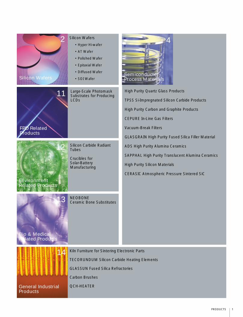
2
High Purity Quartz Glass Products
TPSS Si-Impregnated Silicon Carbide Products
High Purity Carbon and Graphite Products
CEPURE In-Line Gas Filters
Vacuum-Break Filters
GLASGRAIN High Purity Fused Silica Filler Material
ADS High Purity Alumina Ceramics
SAPPHAL High Purity Translucent Alumina Ceramics
High Purity Silicon Materials
CERASIC Atmospheric Pressure Sintered SiC
4
Kiln Furniture for Sintering Electronic Parts
TECORUNDUM Silicon Carbide Heating Elements
GLASSUN Fused Silica Refractories
Carbon Brushes
QCH-HEATER
NEOBONE Ceramic Bone Substitutes
Silicon Carbide RadiantTubes
Crucibles forSolar-BatteryManufacturing
Silicon WafersSemiconductorProcess Materials
Bio & MedicalRelated Products
FPD RelatedProducts
EnvironmentRelated Products
General IndustrialProducts
11
12
13
14
Large-Scale PhotomaskSubstrates for ProducingLCDs
Silicon Wafers
• Hyper Hi-wafer
• AT Wafer
• Polished Wafer
• Epitaxial Wafer
• Diffused Wafer
• SOI Wafer
2 PRODUCTS
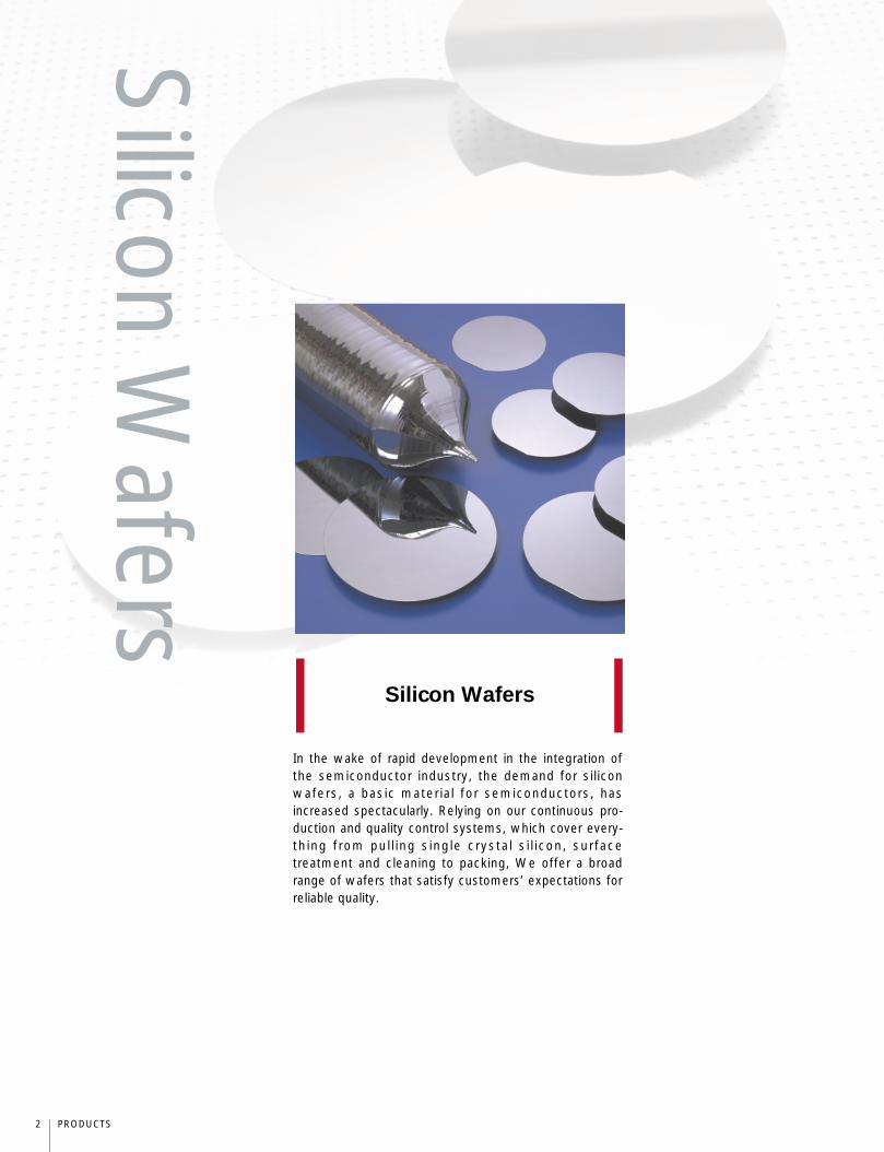
Silicon Wafers
In the wake of rapid development in the integration ofthe semiconductor industry, the demand for siliconwafers, a basic material for semiconductors, hasincreased spectacularly. Relying on our continuous pro-duction and quality control systems, which cover every-thing from pull ing single crystal si l icon, surfacetreatment and cleaning to packing, We offer a broadrange of wafers that satisfy customers’ expectations forreliable quality.
Silicon Wafers
3PRODUCTS
Our diffused wafer is a polished wafer with ahigh density undiffused layer on the back side.They are mainly used as Pw MOS-FET and Biptransistors. The wafers, which accurately reflectspecified diffusion density and diffusion depththrough strict process control, are easy to applyin the user’s manufacturing control, and haveearned a high reputation as superior productswith various advantageous features regardingdevice design.
The Hyper Hi-wafer was developed to supportadvanced devices beyond the 0.18 µm technol-ogy node. Compared with conventional wafers,and even the current Hi-wafer, improvements incrystal growing technology and the optimizationof hydrogen annealing, as well as enhancementsin processing technology, have provided theHyper Hi-wafer with stronger intrinsic getteringability, better flatness and lower Laser ScatteringTopography Defect (LSTD) density. The Hyper Hi-wafer is also superior in terms of electrical proper-ties such as junction leakage. Moreover, theflatness of the Hyper Hi-wafer is excellent for fur-ther miniaturization.
The polished wafer is a silicon wafer with one orboth sides polished to produce a mirror surface.Our polished wafers, which are superior in suchproperties as flatness, cleanliness and getteringcapacity, have earned an excellent reputation forhigh quality and accuracy.
AT wafers, which are created by annealing highquality Si substrate with argon, excel both in thatit lacks surface defects and it has better intrinsicgettering ability. Like the Hyper Hi-wafer, the ATwafer was also developed to support miniatur-ized devices, and it has the added merit of anextremely flat boron profile beneath the wafersurface.
Thick fi lm SOI wafers are widely used in Bi-CMOS and power devices. They exhibit highervoltage endurance and performance speeds, aswell as lower energy consumption, due to theirsilicon-on-insulator structure. We use a bondingmethod in the manufacture of thick film SOIwafers to exercise more precise control over theSOI film thickness and BOX film thickness. Weare also developing an ultra-thin film SOI wafer tomeet the increasing needs of microprocessorsand other such leading-edge devices for higherperformance speed and lower energy consumption.
Our epitaxial wafer is produced by chemicalvapor deposition of single crystal silicon onto thesurface of a polished wafer. In accordance withspecifications, it is used as a substrate on dis-crete devices such as diodes and transistors, andbipolar and MOS integrated circuits. We canmeet a wide range of requirements for multilayerepitaxial wafers, including wafers with an embedded layer.
Hyper Hi-wafer
Polished Wafer
Diffused Wafer
Epitaxial Wafer
SOI Wafer (Silicon-on-insulator wafer)
AT wafer (Argon annealed wafer)
4 PRODUCTS
Semiconductor
Process Materials
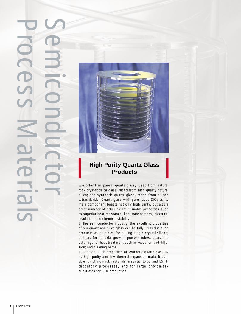
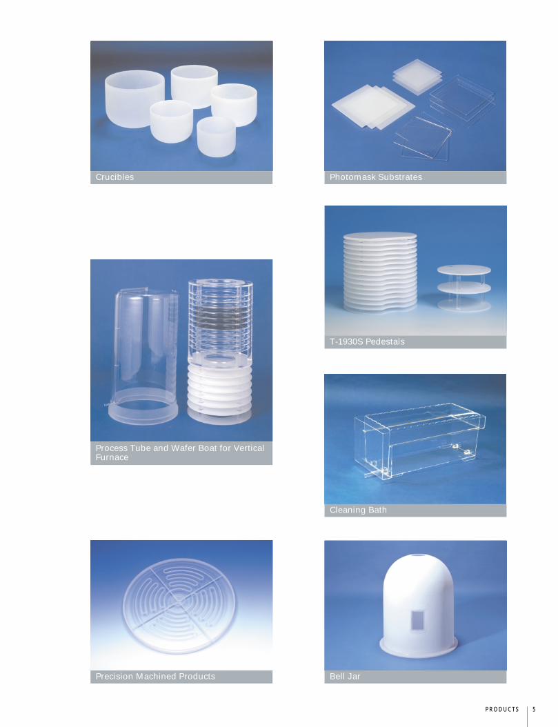
We offer transparent quartz glass, fused from naturalrock crystal; silica glass, fused from high quality naturalsilica; and synthetic quartz glass, made from silicontetrachloride. Quartz glass with pure fused SiO2 as itsmain component boasts not only high purity, but also agreat number of other highly desirable properties suchas superior heat resistance, light transparency, electricalinsulation, and chemical stability.In the semiconductor industry, the excellent propertiesof our quartz and silica glass can be fully utilized in suchproducts as crucibles for pulling single crystal silicon;bell jars for epitaxial growth; process tubes, boats andother jigs for heat treatment such as oxidation and diffu-sion; and cleaning baths.In addition, such properties of synthetic quartz glass asits high purity and low thermal expansion make it suit-able for photomask materials essential to IC and LSI li-thography processes, and for large photomasksubstrates for LCD production.
High Purity Quartz Glass
Products
5PRODUCTS
Bell Jar
Cleaning Bath
T-1930S Pedestals
Photomask Substrates
Process Tube and Wafer Boat for VerticalFurnace
Precision Machined Products
Crucibles
6 PRODUCTS
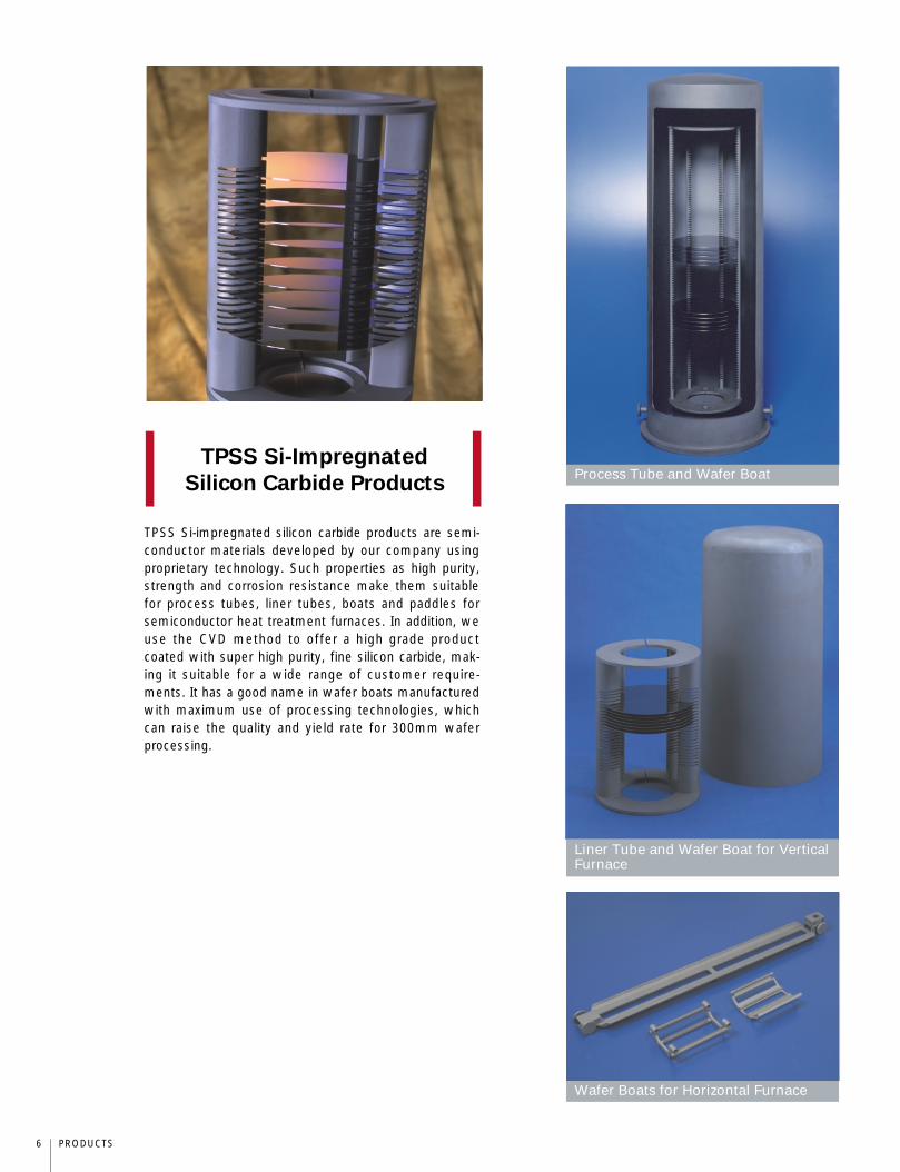
TPSS Si-impregnated silicon carbide products are semi-conductor materials developed by our company usingproprietary technology. Such properties as high purity,strength and corrosion resistance make them suitablefor process tubes, liner tubes, boats and paddles forsemiconductor heat treatment furnaces. In addition, weuse the CVD method to offer a high grade productcoated with super high purity, fine silicon carbide, mak-ing it suitable for a wide range of customer require-ments. It has a good name in wafer boats manufacturedwith maximum use of processing technologies, whichcan raise the quality and yield rate for 300mm wafer processing.
TPSS Si-Impregnated
Silicon Carbide Products
Wafer Boats for Horizontal Furnace
Liner Tube and Wafer Boat for VerticalFurnace
Process Tube and Wafer Boat
7PRODUCTS
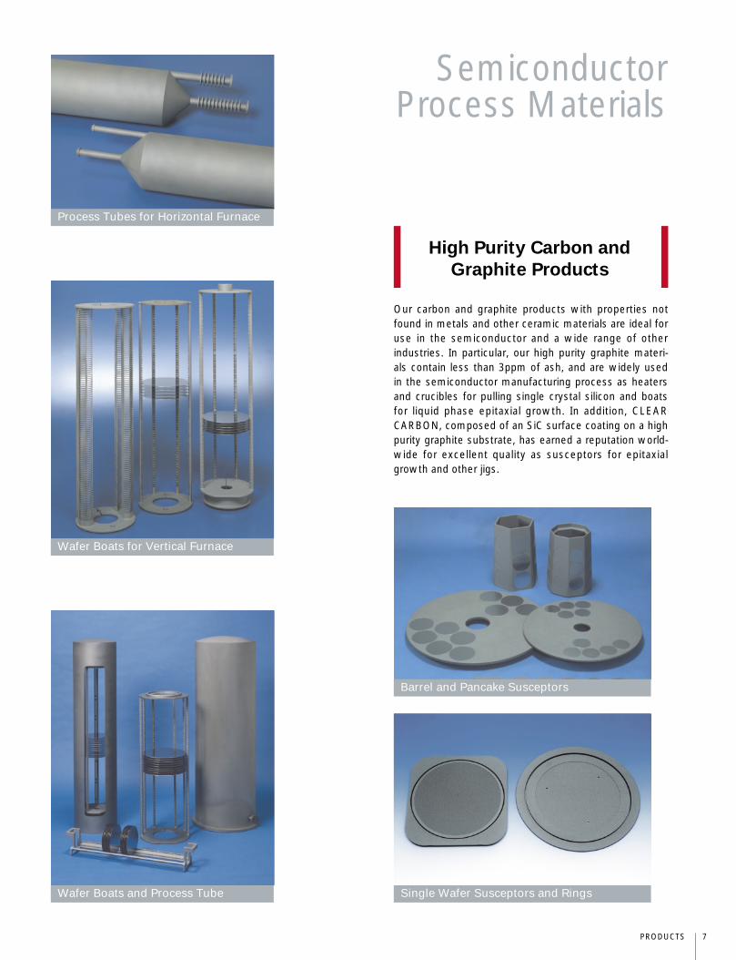
Our carbon and graphite products with properties notfound in metals and other ceramic materials are ideal foruse in the semiconductor and a wide range of otherindustries. In particular, our high purity graphite materi-als contain less than 3ppm of ash, and are widely usedin the semiconductor manufacturing process as heatersand crucibles for pulling single crystal silicon and boatsfor liquid phase epitaxial growth. In addition, CLEARCARBON, composed of an SiC surface coating on a highpurity graphite substrate, has earned a reputation world-wide for excellent quality as susceptors for epitaxialgrowth and other jigs.
High Purity Carbon and
Graphite Products
Wafer Boats and Process Tube
Process Tubes for Horizontal Furnace
Wafer Boats for Vertical Furnace
Single Wafer Susceptors and Rings
Barrel and Pancake Susceptors
SemiconductorProcess Materials
8 PRODUCTS
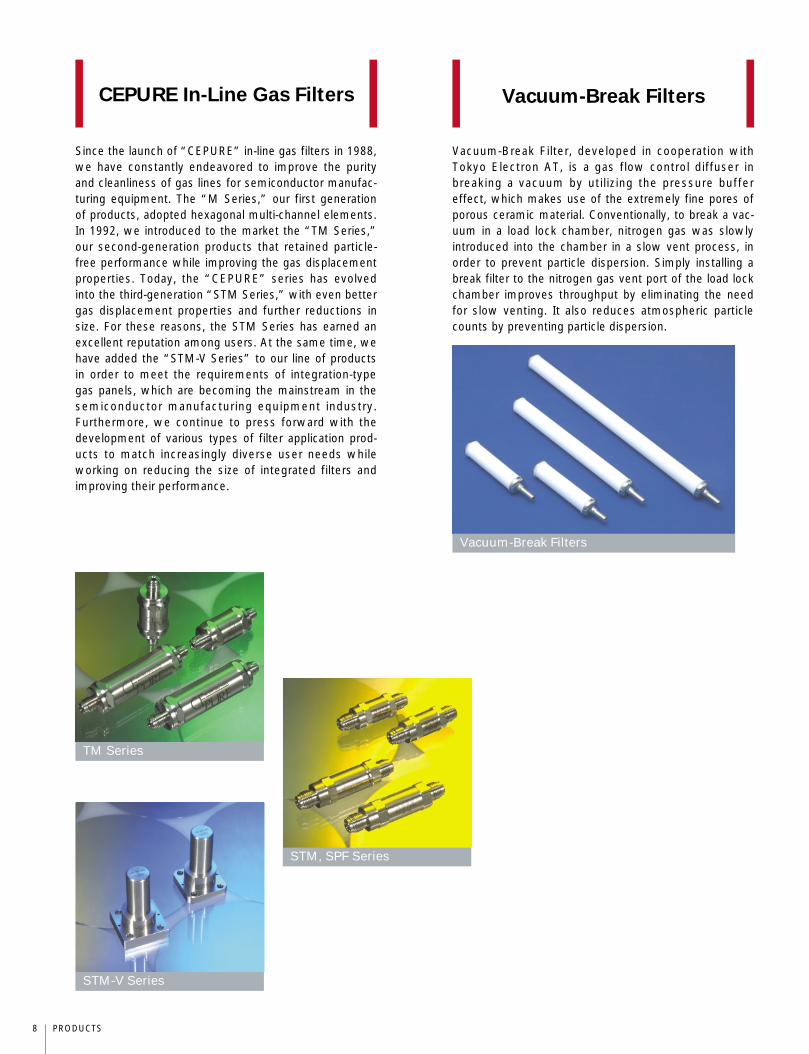
Since the launch of “CEPURE” in-line gas filters in 1988,we have constantly endeavored to improve the purityand cleanliness of gas lines for semiconductor manufac-turing equipment. The “M Series,” our first generationof products, adopted hexagonal multi-channel elements.In 1992, we introduced to the market the “TM Series,”our second-generation products that retained particle-free performance while improving the gas displacementproperties. Today, the “CEPURE” series has evolvedinto the third-generation “STM Series,” with even bettergas displacement properties and further reductions insize. For these reasons, the STM Series has earned anexcellent reputation among users. At the same time, wehave added the “STM-V Series” to our line of productsin order to meet the requirements of integration-typegas panels, which are becoming the mainstream in thesemiconductor manufacturing equipment industry.Furthermore, we continue to press forward with thedevelopment of various types of filter application prod-ucts to match increasingly diverse user needs whileworking on reducing the size of integrated filters andimproving their performance.
CEPURE In-Line Gas Filters
TM Series
STM-V Series
STM, SPF Series
Vacuum-Break Filter, developed in cooperation withTokyo Electron AT, is a gas flow control diffuser inbreaking a vacuum by utilizing the pressure buffereffect, which makes use of the extremely fine pores ofporous ceramic material. Conventionally, to break a vac-uum in a load lock chamber, nitrogen gas was slowlyintroduced into the chamber in a slow vent process, inorder to prevent particle dispersion. Simply installing abreak filter to the nitrogen gas vent port of the load lockchamber improves throughput by eliminating the needfor slow venting. It also reduces atmospheric particlecounts by preventing particle dispersion.
Vacuum-Break Filters
Vacuum-Break Filters
9PRODUCTS
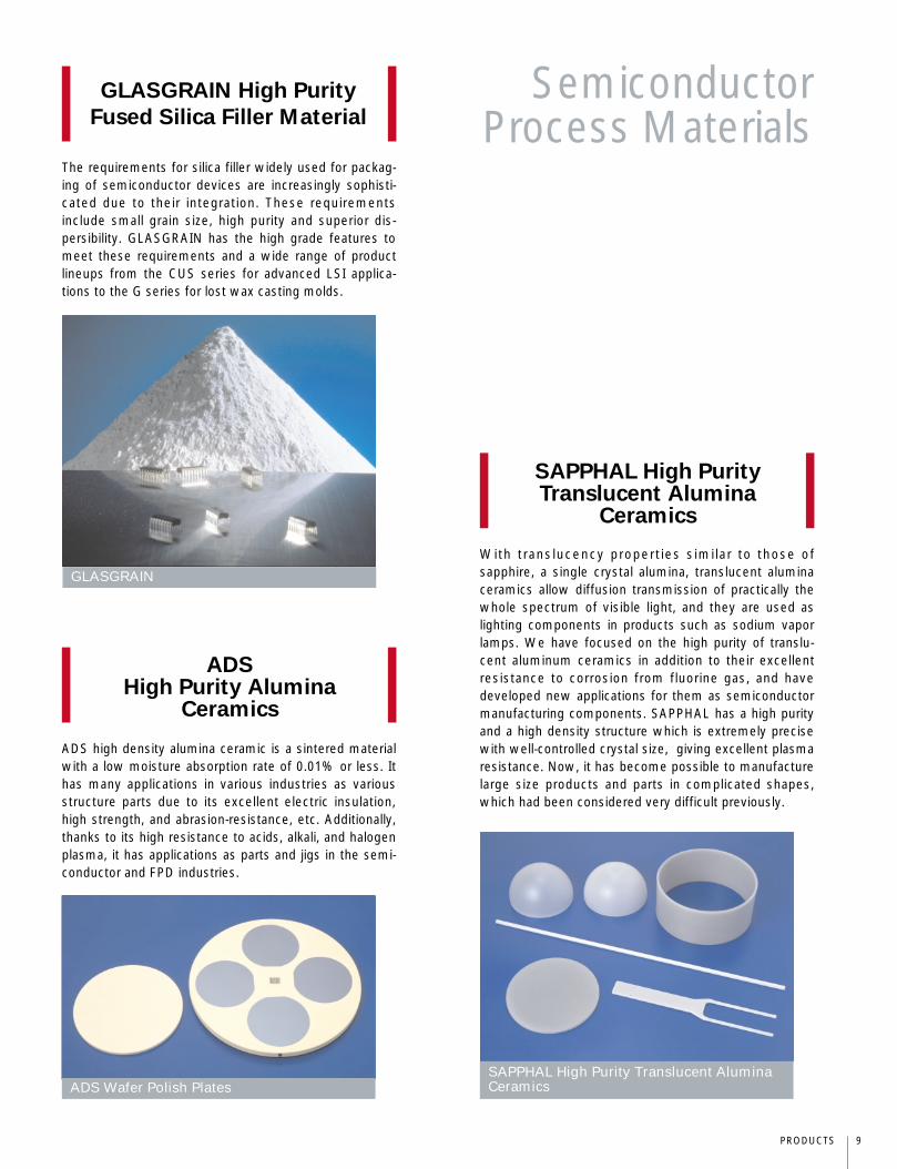
The requirements for silica filler widely used for packag-ing of semiconductor devices are increasingly sophisti-cated due to their integration. These requirementsinclude small grain size, high purity and superior dis-persibility. GLASGRAIN has the high grade features tomeet these requirements and a wide range of productlineups from the CUS series for advanced LSI applica-tions to the G series for lost wax casting molds.
GLASGRAIN High Purity
Fused Silica Filler Material
GLASGRAIN
With translucency properties similar to those of sapphire, a single crystal alumina, translucent aluminaceramics allow diffusion transmission of practically thewhole spectrum of visible light, and they are used aslighting components in products such as sodium vaporlamps. We have focused on the high purity of translu-cent aluminum ceramics in addition to their excellentresistance to corrosion from fluorine gas, and havedeveloped new applications for them as semiconductormanufacturing components. SAPPHAL has a high purityand a high density structure which is extremely precisewith well-controlled crystal size, giving excellent plasmaresistance. Now, it has become possible to manufacturelarge size products and parts in complicated shapes,which had been considered very difficult previously.
SAPPHAL High PurityTranslucent Alumina
Ceramics
SAPPHAL High Purity Translucent AluminaCeramics
SemiconductorProcess Materials
ADS high density alumina ceramic is a sintered materialwith a low moisture absorption rate of 0.01% or less. Ithas many applications in various industries as variousstructure parts due to its excellent electric insulation,high strength, and abrasion-resistance, etc. Additionally,thanks to its high resistance to acids, alkali, and halogenplasma, it has applications as parts and jigs in the semi-conductor and FPD industries.
ADS High Purity Alumina
Ceramics
ADS Wafer Polish Plates
10 PRODUCTS
High purity silicon materials, which have the same puritylevel as silicon wafers, generate almost no contamina-tion and considerably fewer particles. Although the stan-dard material is manufactured in a plate shape, it canalso be produced as a rod or a ring. Furthermore, highprecision machining that was once considered difficultwhen producing parts is now possible. Therefore, thereare great expectations regarding its application in variousprocesses.
High Purity Silicon Materials
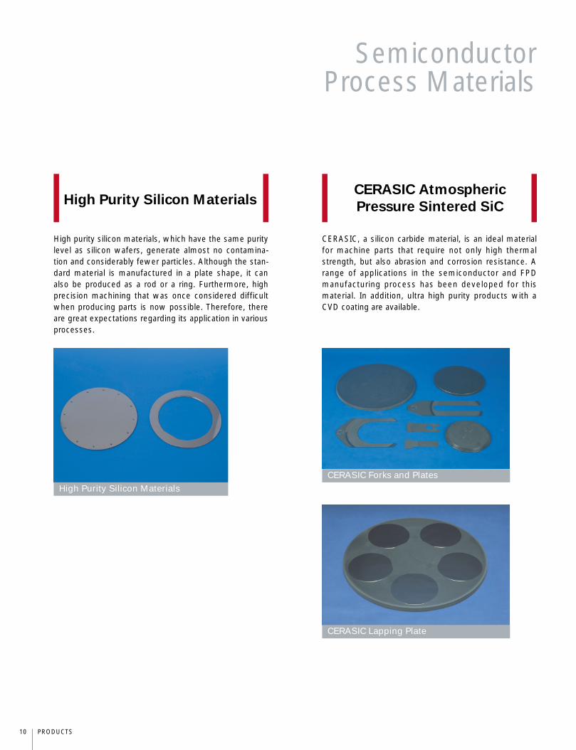
CERASIC, a silicon carbide material, is an ideal materialfor machine parts that require not only high thermalstrength, but also abrasion and corrosion resistance. Arange of applications in the semiconductor and FPDmanufacturing process has been developed for thismaterial. In addition, ultra high purity products with aCVD coating are available.
CERASIC Atmospheric
Pressure Sintered SiC
CERASIC Forks and PlatesHigh Purity Silicon Materials
CERASIC Lapping Plate
SemiconductorProcess Materials
11PRODUCTS
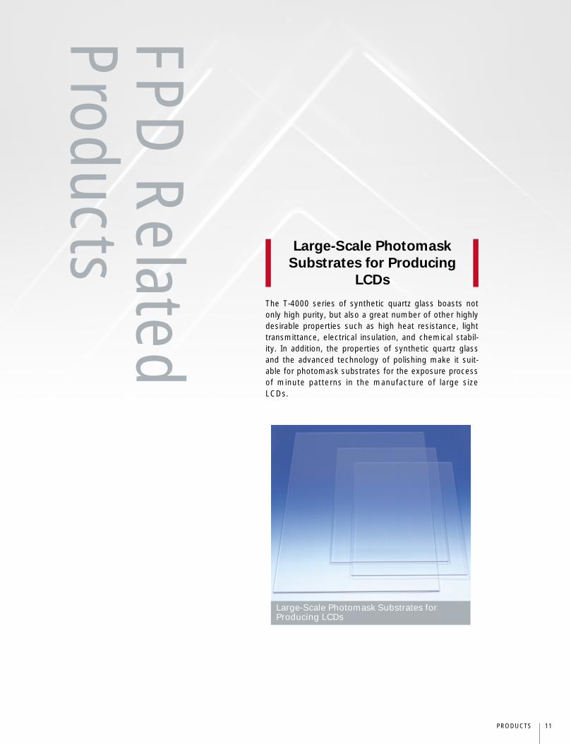
The T-4000 series of synthetic quartz glass boasts notonly high purity, but also a great number of other highlydesirable properties such as high heat resistance, lighttransmittance, electrical insulation, and chemical stabil-ity. In addition, the properties of synthetic quartz glassand the advanced technology of polishing make it suit-able for photomask substrates for the exposure processof minute patterns in the manufacture of large sizeLCDs.
Large-Scale Photomask
Substrates for Producing
LCDs
Large-Scale Photomask Substrates forProducing LCDs
FPD R
elatedProducts
12 PRODUCTS
CERASIC, a silicon carbide material, is a ceramic mater-ial that has superior properties in terms of machining,and abrasion and corrosion-resistance to corrosive gasesand chemicals. It is widely used in heat-treatment, andits long life property makes it a recognized contributor tolow running costs and the reduction of industrial waste.In addition, we can make large-scale products of1000mm or more, which is the largest size in the worldfor ceramic materials. (Plates:1000 X1000mm or more,Tubes: 2000mm or more in length)
Silicon Carbide
Radiant Tubes
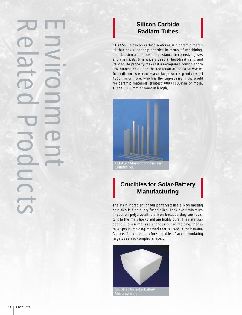
The main ingredient of our polycrystalline silicon meltingcrucibles is high purity fused silica. They exert minimumimpact on polycrystalline silicon because they are resis-tant to thermal shocks and are highly pure. They are sus-ceptible to minimal size changes during molding, thanksto a special molding method that is used in their manu-facture. They are therefore capable of accommodatinglarge sizes and complex shapes.
Crucibles for Solar-Battery
Manufacturing
CERASIC Atmospheric PressureSintered SiC
Crucibles for Solar-batteryManufacturing
Environment
Related Products
13PRODUCTS
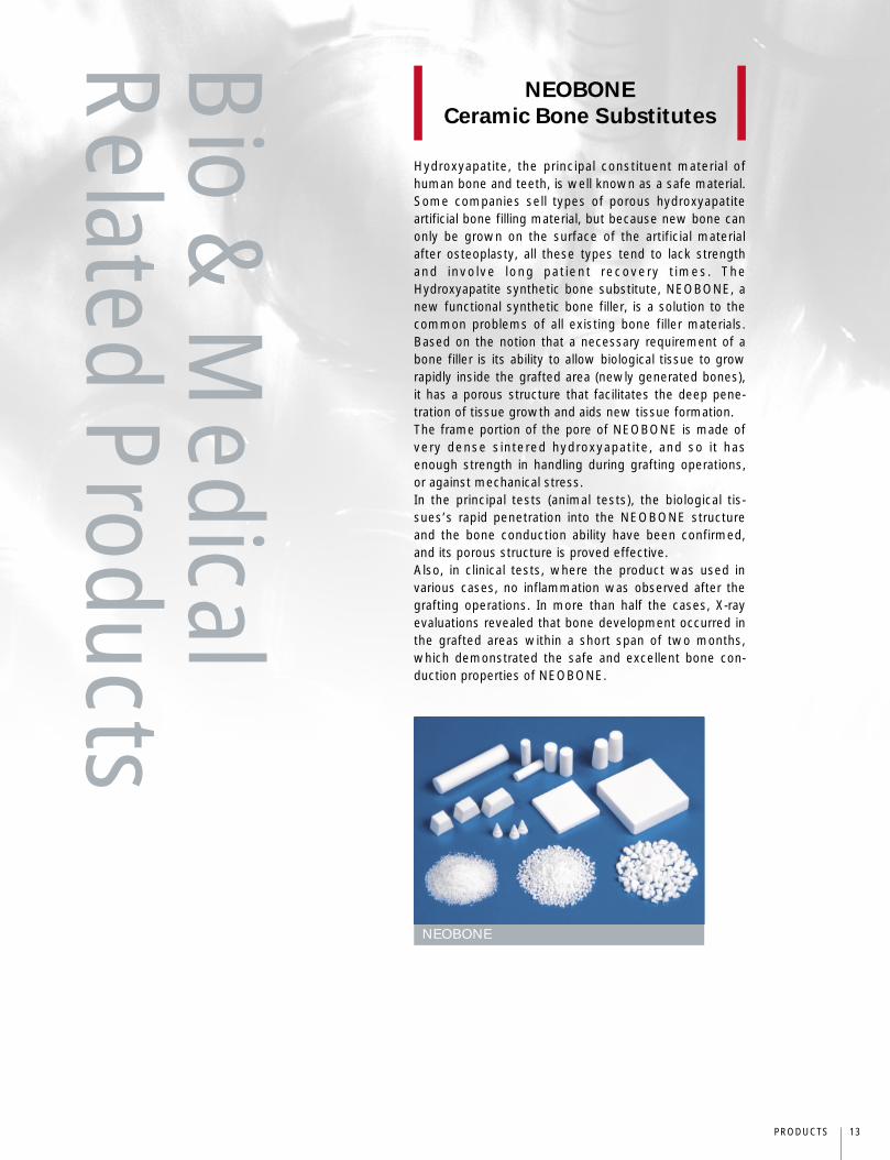
Hydroxyapatite, the principal constituent material ofhuman bone and teeth, is well known as a safe material.Some companies sell types of porous hydroxyapatiteartificial bone filling material, but because new bone canonly be grown on the surface of the artificial materialafter osteoplasty, all these types tend to lack strengthand involve long patient recovery times. TheHydroxyapatite synthetic bone substitute, NEOBONE, anew functional synthetic bone filler, is a solution to thecommon problems of all existing bone filler materials.Based on the notion that a necessary requirement of abone filler is its ability to allow biological tissue to growrapidly inside the grafted area (newly generated bones),it has a porous structure that facilitates the deep pene-tration of tissue growth and aids new tissue formation.The frame portion of the pore of NEOBONE is made ofvery dense sintered hydroxyapatite, and so it hasenough strength in handling during grafting operations,or against mechanical stress.In the principal tests (animal tests), the biological tis-sues’s rapid penetration into the NEOBONE structureand the bone conduction ability have been confirmed,and its porous structure is proved effective.Also, in clinical tests, where the product was used invarious cases, no inflammation was observed after thegrafting operations. In more than half the cases, X-rayevaluations revealed that bone development occurred inthe grafted areas within a short span of two months,which demonstrated the safe and excellent bone con-duction properties of NEOBONE.
NEOBONE
Ceramic Bone Substitutes
NEOBONE
Bio &
Medical
Related Products
14 PRODUCTS
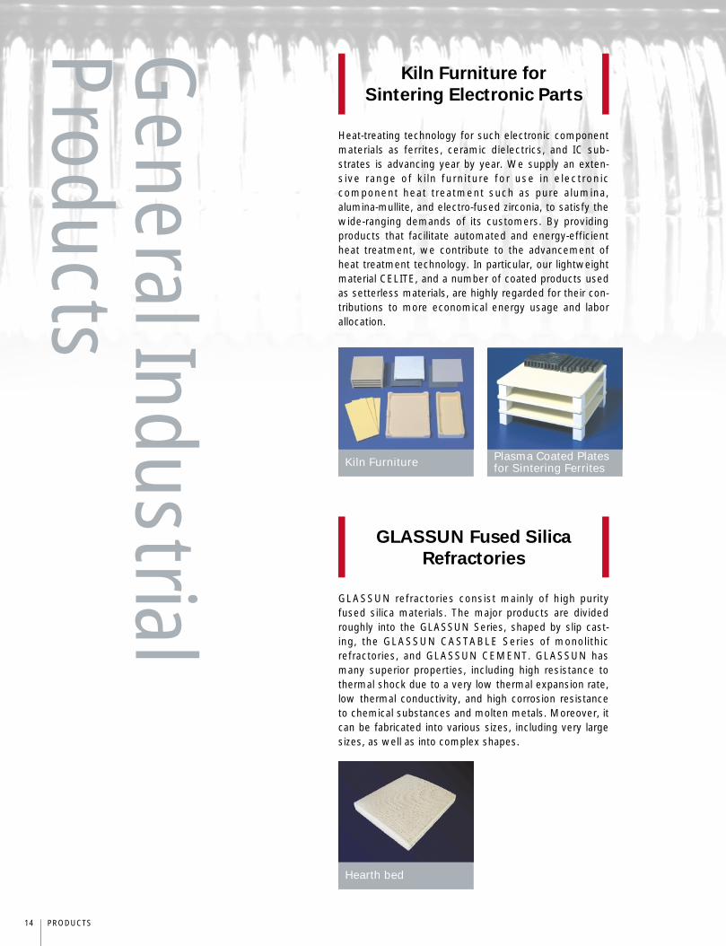
Heat-treating technology for such electronic componentmaterials as ferrites, ceramic dielectrics, and IC sub-strates is advancing year by year. We supply an exten-sive range of ki ln furniture for use in electroniccomponent heat treatment such as pure alumina, alumina-mullite, and electro-fused zirconia, to satisfy thewide-ranging demands of its customers. By providingproducts that facilitate automated and energy-efficientheat treatment, we contribute to the advancement ofheat treatment technology. In particular, our lightweightmaterial CELITE, and a number of coated products usedas setterless materials, are highly regarded for their con-tributions to more economical energy usage and laborallocation.
Kiln Furniture for
Sintering Electronic Parts
Kiln Furniture
Hearth bed
GLASSUN refractories consist mainly of high purityfused silica materials. The major products are dividedroughly into the GLASSUN Series, shaped by slip cast-ing, the GLASSUN CASTABLE Series of monolithicrefractories, and GLASSUN CEMENT. GLASSUN hasmany superior properties, including high resistance tothermal shock due to a very low thermal expansion rate,low thermal conductivity, and high corrosion resistanceto chemical substances and molten metals. Moreover, itcan be fabricated into various sizes, including very largesizes, as well as into complex shapes.
GLASSUN Fused Silica
Refractories
Plasma Coated Platesfor Sintering Ferrites
General Industrial
Products
15PRODUCTS
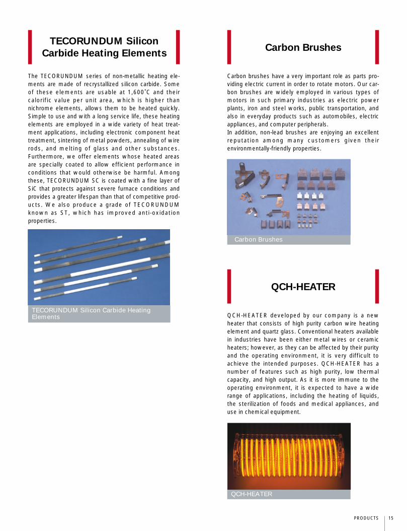
The TECORUNDUM series of non-metallic heating ele-ments are made of recrystallized silicon carbide. Someof these elements are usable at 1,600˚C and theircalorific value per unit area, which is higher thannichrome elements, allows them to be heated quickly.Simple to use and with a long service life, these heatingelements are employed in a wide variety of heat treat-ment applications, including electronic component heattreatment, sintering of metal powders, annealing of wirerods, and melting of glass and other substances.Furthermore, we offer elements whose heated areasare specially coated to allow efficient performance inconditions that would otherwise be harmful. Amongthese, TECORUNDUM SC is coated with a fine layer ofSiC that protects against severe furnace conditions andprovides a greater lifespan than that of competitive prod-ucts. We also produce a grade of TECORUNDUMknown as ST, which has improved anti-oxidation properties.
TECORUNDUM Silicon
Carbide Heating Elements
TECORUNDUM Silicon Carbide HeatingElements
Carbon brushes have a very important role as parts pro-viding electric current in order to rotate motors. Our car-bon brushes are widely employed in various types ofmotors in such primary industries as electric powerplants, iron and steel works, public transportation, andalso in everyday products such as automobiles, electricappliances, and computer peripherals. In addition, non-lead brushes are enjoying an excellentreputation among many customers given their environmentally-friendly properties.
Carbon Brushes
Carbon Brushes
QCH-HEATER developed by our company is a newheater that consists of high purity carbon wire heatingelement and quartz glass. Conventional heaters availablein industries have been either metal wires or ceramicheaters; however, as they can be affected by their purityand the operating environment, it is very difficult toachieve the intended purposes. QCH-HEATER has anumber of features such as high purity, low thermalcapacity, and high output. As it is more immune to theoperating environment, it is expected to have a widerange of applications, including the heating of liquids,the sterilization of foods and medical appliances, anduse in chemical equipment.
QCH-HEATER
QCH-HEATER
16 PRODUCTS
Covalent Materials USA, Inc.
Head Office:2010 N. 1st Street, Suite 400, San Jose, California 95131-2018, U.S.A.Tel: +1-408-467-0515Fax: +1-408-467-0510
Texas Office:300E. Royal Lane, Suite 107, Irving, Texas 75039, U.S.A.Tel: +1-972-444-0277Fax: +1-972-444-0980
Covalent Materials Europe GmbH
Herzog-Heinrich-Strasse 11, 80336 Munich, GermanyTel: +49 (0) 89 55 14 19 0Fax: +49 (0) 89 55 14 19 40
Covalent Materials Korea Ltd.
Rm 1505, Hibrand Bldg., 215, Yangjae-Dong, Seocho-ku, Seoul, Korea 137-924Tel: +82- (0) 2-2155-2225Fax: +82- (0) 2-2155-2226
Covalent Materials Taiwan Corp.
8F-2, No. 289, Sec. 2, Kuang-Fu Road, Hsin-Chu, 30071, TaiwanTel: +886 (0) 3-575-1238Fax: +886 (0) 3-575-1633
OVERSEAS
17PRODUCTS
The Covalent Group
— Creating New Values through Collective Strength —
Covalent is used in the chemistry terms “covalent bond”and “covalent crystal,” and it refers to chemical bondsformed by the sharing of electrons between atoms.
We bring together our ceramics and silicon technologies tocreate new values, and are determined to grow with thepeople who have a connection with us. These are the ideasbehind our new company name “Covalent Materials.”
The vertical bars on either side of COVALENT represent themathematical symbol for the absolute value, and signifyour advanced technologies and strong will.
Through collective strength, we are committed to creatingnew values and better serving the users of our productsand all other stakeholders.
Nissei Bldg., 6-3, Osaki 1-chome, Shinagawa-ku,Tokyo 141-0032, JapanTel: +81-3-5437-8411Fax: +81-3-5437-7172www.covalent.co.jp


![(MLV) MULTILAYER CHIP VARISTOR - fenghua.comfenghua.com/pdf/varistor/chip_varistor.pdf · (MLV) MULTILAYER CHIP VARISTOR Multilayer Chip ... [2220] 8063[3225] 1080[4032] 55 125 V](https://img.pdfslide.us/doc/110x75/5b42af3a7f8b9ad23b8b5240/mlv-multilayer-chip-varistor-mlv-multilayer-chip-varistor-multilayer-chip.jpg)