Embed Size (px)
Citation preview

Revision. 003
Page 1 of 11
Product Standards
Established: 2016-09-01 Revised: 2017-01-16
PGA26E07BA
PGA26E07BA

Revision. 003
Page 2 of 11
Established: 2016-09-01 Revised: 2017-01-16
PGA26E07BA
Type GaN-Tr
Application For power switching
Structure N-channel enhancement mode FET
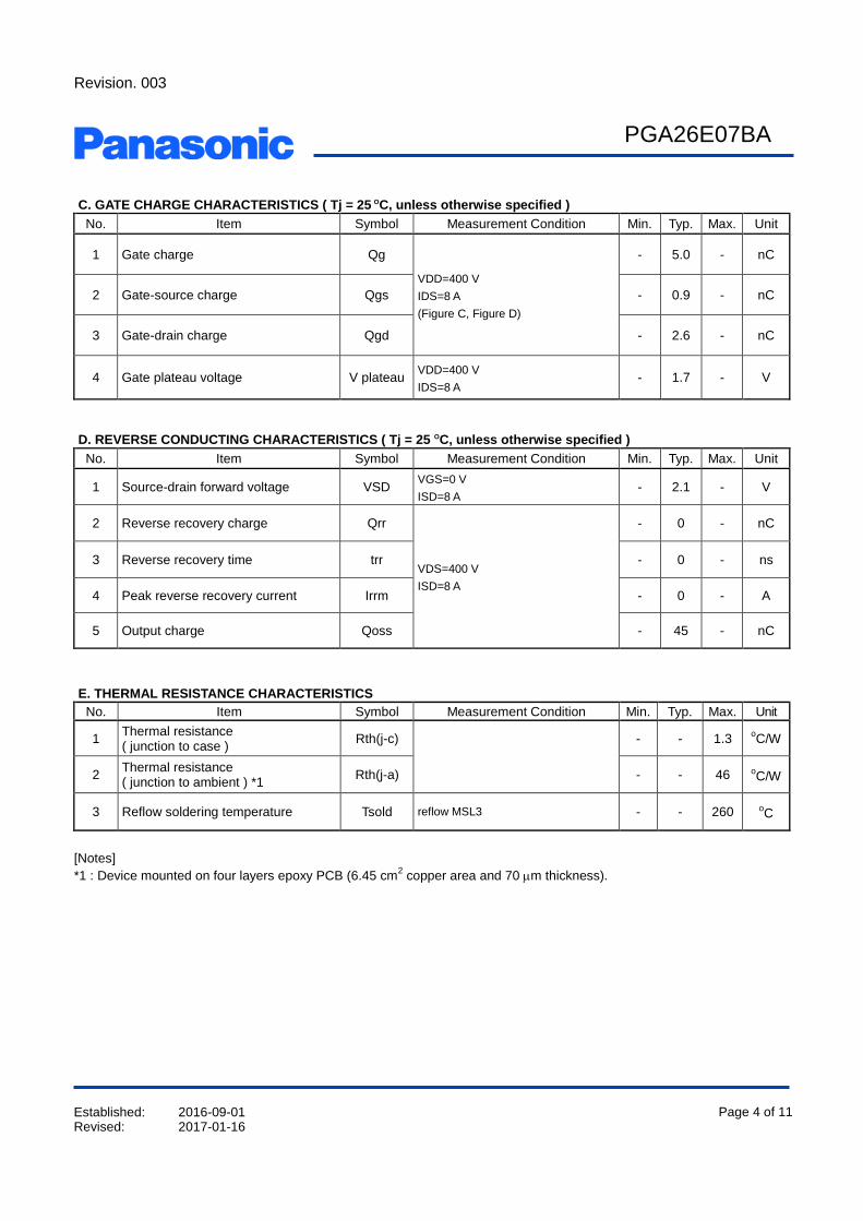
Equivalent Circuit Figure 1
Out Line DFN 8X8 Marking PGA26E07
A. ABSOLUTE MAXIMUM RATINGS ( Tj = 25 OC , unless otherwise specified )
No. Item Symbol Values
Unit Note Min. Typ. Max.
1 Drain-source voltage ( DC ) *1 VDSS - - 600 V
2 Drain-source voltage ( pulse ) *2 VDSP - - 750 V
3 Gate-source voltage ( DC ) *1 VGSS -10 - - V *VGSS+ is given by IG ratings
*See application note
4 Gate current ( DC ) *1 IG - - 50 mA *See application note
5 Gate current ( pulse ) *3,4 IGP - - 1.5 A *See application note
6 Electric gate charge QGP - - 32 nC *f=200kHz
*See application note
7 Drain current ( DC ) ( Tc = 25 OC ) *1
ID - - 26 A Figure 4
8 Drain reverse current ( DC ) ( Tc = 25 OC ) *1
IDR - - 26 A
9 Drain current ( pulse )*5 ( Tc = 25 OC )*1
ID pulse - - 61 A Figure 4
10 Drain reverse current ( pulse )*5 ( Tc = 25 OC )*1
IDR pulse - - 61 A
11 Power dissipation ( Tc = 25 OC ) PD - - 96 W Figure 2
12 Junction temperature Tj - - 150 OC
13 Storage temperature Tstg -55 - 150 OC
14 Drain-source voltage slope dv/dt - - 200 V/ns
[Special instructions]
*1 : Please use this product to meet a condition of Tj within 150 OC.
*2 : Spike duty cycle D < 0.1, spike duration < 1us, total spike time < 1hour.
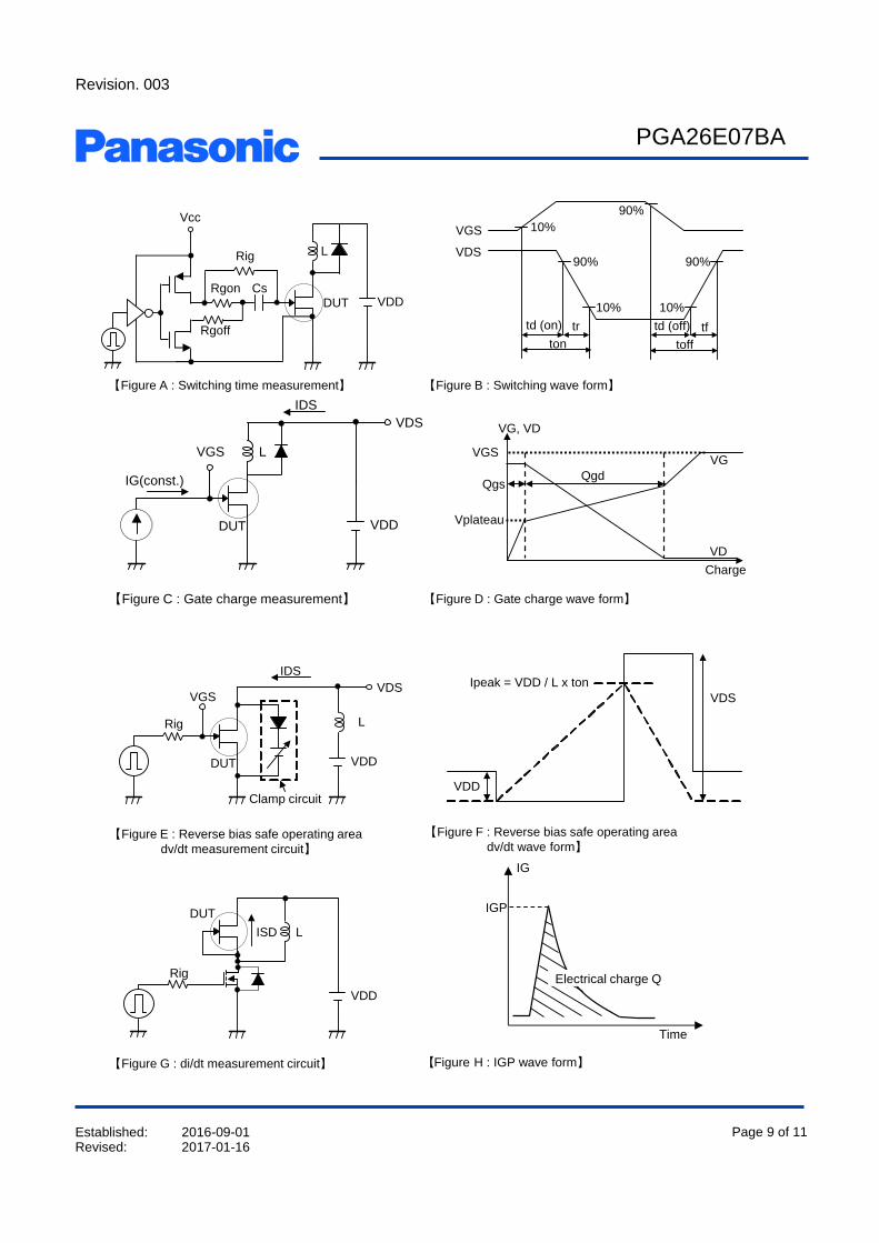
*3 : IGP is defined as (Vcc - Vplateau) / Rgon, as shown in Figure A.
Vplateau is the voltage between Gate and Source1.
*4 : Please use this product to meet both a maximum gate current and a maximum gate pulse charge
of IGP(1.5A) and Q(32nC) respectively, as shown in Figure H.
*5 : Pulse width limited by Tjmax.

Revision. 003
Page 3 of 11
Established: 2016-09-01 Revised: 2017-01-16
PGA26E07BA
B. ELECTRICAL CHARACTERISTICS ( Tj = 25 OC , unless otherwise specified )
No. Item Symbol Measurement Condition Min. Typ. Max. Unit
1 Drain cut-off current IDSS
VDS=600 V, VGS=0 V, Tj=25 oC - - 100 μA
VDS=600 V, VGS=0 V, Tj=150 oC - 100 - μA
2 Gate-source leakage current IGSS VGS=-3 V
VDS=0 V -1 - - μA
3 Gate forward voltage VGSF IGS=26.1 mA
open drain 2.8 3.5 4.2 V
4 Gate threshold voltage VTH VDS=10 V
IDS=2.6 mA 0.9 1.2 1.6 V
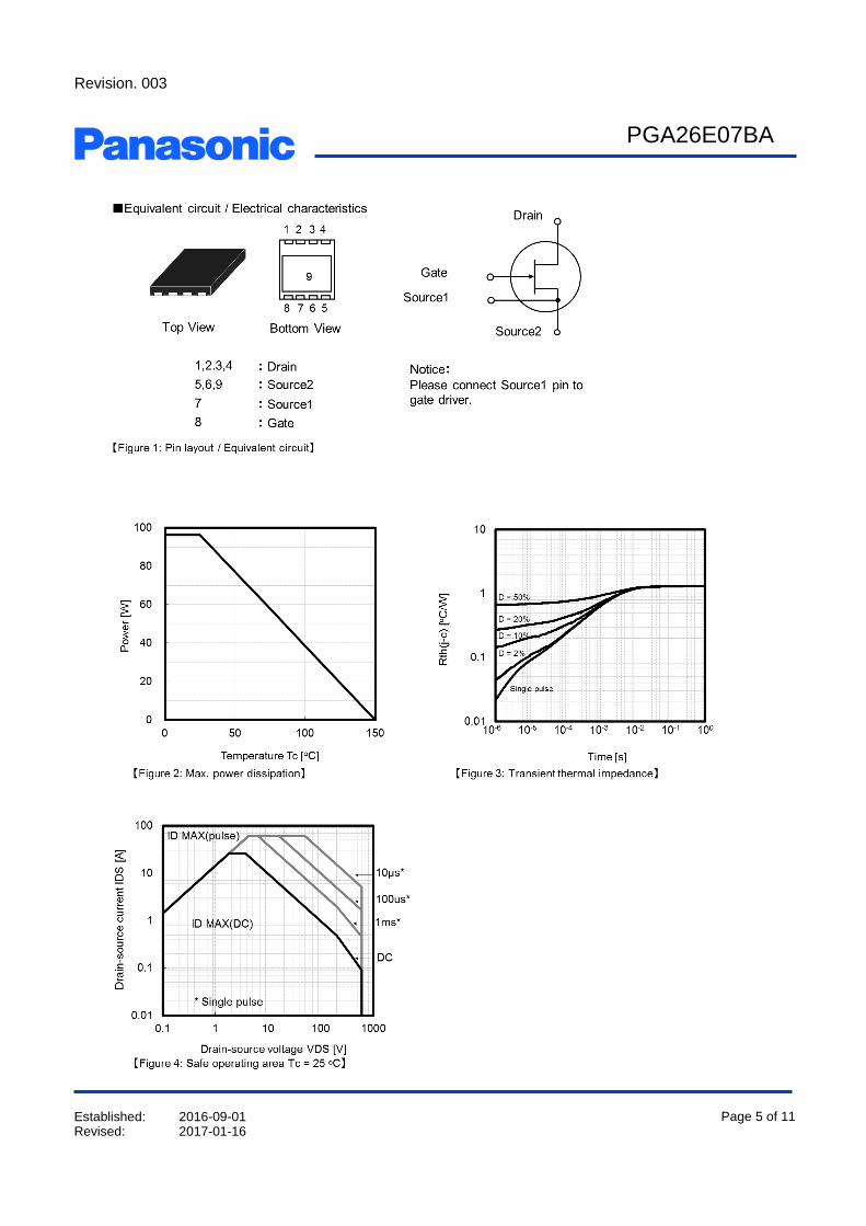
5 Drain-source on-state resistance RDS(on)
IGS=26.1 mA, IDS=8A, Tj=25 oC - 56 70 mΩ
IGS=26.1 mA, IDS=8 A, Tj=150 oC - 110 - mΩ
6 Gate resistance RG f=100MHz
open drain - 0.6 - Ω
7 Transfer conductance gfs VDS=8 V
IDS=8 A - 32 - S
8 Input capacitance Ciss
VDS=400 V
VGS=0 V
f=1 MHz
- 405 - pF
9 Output capacitance Coss - 71 - pF
10 Reverse transfer capacitance Crss - 0.4 - pF
11 Turn-on delay time td(on) VDD=400 V
IDS=8 A
(Figure A, Figure B)
Vcc=12 V
Rgon=6.2 Ω, Rgoff=4.7 Ω,
Rig=680 Ω, Cs=1500 pF
- 3.7 - ns
12 Rise time tr - 5.6 - ns
13 Turn-off delay time td(off) - 5.5 - ns
14 Fall time tf - 2.4 - ns
15 Effective output capacitance
( energy related ) Co(er)
VDS=0-480 V
- 87 - pF
16 Effective output capacitance
( time related ) Co(tr) - 106 - pF
Revision. 003
Page 4 of 11
Established: 2016-09-01 Revised: 2017-01-16
PGA26E07BA
C. GATE CHARGE CHARACTERISTICS ( Tj = 25 OC, unless otherwise specified )
No. Item Symbol Measurement Condition Min. Typ. Max. Unit
1 Gate charge Qg
VDD=400 V
IDS=8 A
(Figure C, Figure D)
- 5.0 - nC
2 Gate-source charge Qgs - 0.9 - nC
3 Gate-drain charge Qgd - 2.6 - nC
4 Gate plateau voltage V plateau VDD=400 V
IDS=8 A - 1.7 - V
D. REVERSE CONDUCTING CHARACTERISTICS ( Tj = 25 OC, unless otherwise specified )
No. Item Symbol Measurement Condition Min. Typ. Max. Unit
1 Source-drain forward voltage VSD VGS=0 V
ISD=8 A - 2.1 - V
2 Reverse recovery charge Qrr
VDS=400 V
ISD=8 A
- 0 - nC
3 Reverse recovery time trr - 0 - ns
4 Peak reverse recovery current Irrm - 0 - A
5 Output charge Qoss - 45 - nC
E. THERMAL RESISTANCE CHARACTERISTICS
No. Item Symbol Measurement Condition Min. Typ. Max. Unit
1 Thermal resistance ( junction to case )
Rth(j-c)
- - 1.3 oC/W
2 Thermal resistance ( junction to ambient ) *1
Rth(j-a) - - 46 oC/W
3 Reflow soldering temperature Tsold reflow MSL3 - - 260 oC
[Notes]
*1 : Device mounted on four layers epoxy PCB (6.45 cm2 copper area and 70 m thickness).
Revision. 003
Page 5 of 11
Established: 2016-09-01 Revised: 2017-01-16
PGA26E07BA
Revision. 003
Page 6 of 11
Established: 2016-09-01 Revised: 2017-01-16
PGA26E07BA

Revision. 003
Page 7 of 11
Established: 2016-09-01 Revised: 2017-01-16
PGA26E07BA

Revision. 003
Page 8 of 11
Established: 2016-09-01 Revised: 2017-01-16
PGA26E07BA
Revision. 003
Page 9 of 11
Established: 2016-09-01 Revised: 2017-01-16
PGA26E07BA
【Figure H : di/dt wave form】
ISDtrr
Irrm
Irrm ×10%
Qrr
【Figure B : Switching wave form】
【Figure D : Gate charge wave form】
【Figure E : Reverse bias safe operating area
dv/dt measurement circuit】
【Figure G : di/dt measurement circuit】
【Figure F : Reverse bias safe operating area
dv/dt wave form】
VDD
ISD
Rig
DUT
L
VGS
Vplateau
QgsQgd
VG, VD
Charge
VD
VG
VGS
VDS
10%
90%
90%90%
10% 10%
tr
ton
tf
toff
td (off)td (on)
VDS
VDD
Ipeak = VDD / L x ton
【Figure A : Switching time measurement】
VGS
DUT VDD
L
VDS
IDS
Rig
Clamp circuit
【Figure C : Gate charge measurement】
VGS
DUT VDD
RL
VDS
IDS
Rig
VDDDUTRgon Cs
Rig L
Vcc
Rgoff
VGS
IG(const.)
DUT VDD
VDS
IDS
【Figure C : Gate charge measurement】
L
Time
IG
Electrical charge Q
IGP
【Figure H : IGP wave form】

Revision. 003
Page 10 of 11
Established: 2016-09-01 Revised: 2017-01-16
PGA26E07BA
[Precautions for Use] 1) The product has risks for break-down or burst or giving off smoke in following conditions. Avoid the following use. Fuse
should be added at the input side or connect zener diode between Gate pin and GND, etc as a countermeasure to pass regulatory Safety Standard. Concrete countermeasure could be provided individually. However, customer should make the final judgment.
(1) Reverse the Drain pin and gate pin connection to the power supply board.
(2) Drain pin short to Source1 pin and Source2 pin.
(3) Drain pin short to Gate pin.
(4) Gate pin open.

Revision. 003
Page 11 of 11
Established: 2016-09-01 Revised: 2017-01-16
PGA26E07BA
■ Outline Unit: mm
e
A
D
E1
E2
E3
L
D1
b
E
A2
A1
D2
SYMBOLDIMENSION
MIN NOM MAX
A 1.15 1.25 1.35
A1 0.00 0.02 0.05
A2 0.40 0.50 0.60
b 0.90 1.00 1.10
D 7.90 8.00 8.10
D1 6.84 6.94 7.04
D2 0.40 0.50 0.60
E 7.90 8.00 8.10
E1 0.90 1.00 1.10
E2 3.10 3.20 3.30
E3 2.70 2.80 2.90
e 2.00 B.S.C.
L 0.40 0.50 0.60
1234
5 6 7 8
9