Embed Size (px)
Citation preview

Product Specification
T177B04N00
(REVISION 1)
Crystal Clear Technology Sdn. Bhd. 16 Jalan TP5, Taman Perindustrian Sime UEP,
47600 Subang Jaya, Selangor DE
Tel: +603-80247099
Website: www.cct.com.my
_____________________________________________________________________________________

CRYSTAL CLEAR TECHNOLOGY SDN. BHD Spec No. T177B04N00 REV1
1
1.0 Table of Contents
No Title Page
1 Table of Contents 1
2 Record of revision 2
3 General Specification 3
4 Absolute Maximum Ratings 4
5 Electrical Characteristics and Instruction Code 5
6 Optical Characteristics 7
7 AC Characteristics 10
8 Initial Code Setting (Recommend) 12
9 RA Test Condition 14
10 Inspection Criteria 16
11 Precaution and Limited Warranty 17
12 Mechanical Specification 21

CRYSTAL CLEAR TECHNOLOGY SDN. BHD Spec No. T177B04N00 REV1
2
2.0 Records of Revision
Rev Date Item Page Comment Originator Checked By
1.0 23.01.17 Initial Release Azhar Liew

CRYSTAL CLEAR TECHNOLOGY SDN. BHD Spec No. T177B04N00 REV1
3
3.0 General Specification
T177B04N00 is 1.77” color TFT-LCD (Thin Film Transistor Liquid Crystal Display) module composed of LCD panel, driver ICs control circuit, LED backlight and Touch Panel.
This display area contains 128 x 160 pixels. This product compliant with RoHS environmental requirement.
Item Contents Unit Note
LCD Type 1.77 “ TFT -
Display color 65k 1
Viewing Direction (Optimum)
6 O’clock
Module size 34.0 X 43.7 X 2.55 mm 2
Active Area(W×H) 28.03 X 35.04 mm
Number of Dots 128×RGB×160 dots
Controller ST7735S or equivalent -
Interface Type MCU-8Bit -
Input Voltage 2.8 V
Power Consumption (without Backlight)
6 mw
Backlight 2-LEDs (white) pcs
System Interface Mode Parallel/Serial - Note 1: Color tone is slightly changed by temperature and driving voltage. Note 2: FPC or wire are not included.

CRYSTAL CLEAR TECHNOLOGY SDN. BHD Spec No. T177B04N00 REV1
4
4.0 Absolute Maximum Ratings 4.1 Electrical Absolute Maximum ratings (Vss = 0V, Ta = 25°C)
Item Symbol Min. Max. Unit Note
Power Supply Voltage VCC -0.3 4.8 V
1, 2
Logic Signal Input /Output Voltage
VIOVCC -0.3 VCC+0.3 V
Operating Temperature TOP -20 70 °C
Storage Temperature TST -30 80 °C
Current of LED ILED 0 30 mA/led
Notes:
1. If the module is above these absolute maximum ratings. It may become permanently damaged.
2. VCC >VSS must be maintained. 3. Please be sure users are grounded when handing LCD Module. 4.
4.2 Environmental Absolute Maximum Ratings
Item Storage Operating
Note MIN. MAX. MIN. MAX.
Ambient Temperature -20℃ 70℃ -10℃ 60℃ 1,2
Humidity - - - - 3
1. The response time will become lower when operated at low temperature. 2. Background color changes slightly depending on ambient temperature. The
phenomenon is reversible. 3. Ta<=60°C and 85%RH MAX.
(Ta>=60°C. Absolute humidity must be lower than the humidity of 90%RH at
60°C)

CRYSTAL CLEAR TECHNOLOGY SDN. BHD Spec No. T177B04N00 REV1
5
5.0 Electrical Characteristics and Instruction Code
5.1 Electrical Characteristics (Vss = 0V, Ta = 25°C)
Note: 1: When an optimum contrast is obtained in transmissive mode. 2: Tested in 1X1 chessboard pattern.
5.2 LED Backlight Specification (Vss = 0V, Ta = 25°C)
Note: 1. VLED=VLED (+)-VLED (-). 2. It is recommended that customer supply constant current to prolong the led
lifetime and optimum led performance
Parameter Symbol Condition Min Typ Max Unit Note
Power supply VCC/V
CI Ta=25℃ 2.7 3.8 3.9 V
Input Current IDD - 2 4 mA
Input voltage
‘H’ VIH 0.78VCC - VCC V
‘L’ VIL -0.3 - 0.2 VCC V
Output Voltage H VOH 0.8VCC - VCC V
Output Voltage L VOL GND - 0.2VCC V
Item Symbol Condition Min Typ Max Unit Note
Supply Voltage VLED - 2.9 3.1 3.3 V 1
Supply Current If - - 30 - mA 2
Luminance Lv If = 30mA - 3000 - cd/m2
Number Of LED - - - 2 - Piece
Connection Mode P - - Parallel -

CRYSTAL CLEAR TECHNOLOGY SDN. BHD Spec No. T177B04N00 REV1
6
5.3 Interface Signal
Pin No. Symbol I/O Function
1 SPI4W 0:3-Lline Enable 1:4 line Enable
2 RDX Read Signal
3 D/CX_SCL Register Selection Signal
4 DB0_SDA Data Bus
5 DV1 Data Bus
6 DB2 Data Bus
7 DB3 Data Bus
8 DB4 Data Bus
9 DB5 Data Bus
10 DB6 Data Bus
11 DB7 Data Bus
12 RESX Reset Signal
13 CSX Chip Selection Pin
14 IM2 0: Serial Interface; 1: Parallel Interface
15 WRX/D/CX Write Signal
16 IOVCC 1.8V I/O Power Supply
17 VCC 2.8V Power supply Power Supply
18 GND 0V Ground
19 LEDA / Anode of Backlight LED
20 LEDK / Cathode of Backlight LED

CRYSTAL CLEAR TECHNOLOGY SDN. BHD Spec No. T177B04N00 REV1
7
6.0 Optical Characteristics
Item Symbol Condition Min. Typ. Max. Unit Note
Brightness Bp θ=0°
Φ=0°
220 250 - Cd/m2 1
Uniformity ⊿Bp 80 - - % 1,2
Viewing Angle
Ø = 90°
Cr≥10
20 -
Deg 3 Ø = 270° 55 -
Ø = 0° 55 -
Ø = 180° 55 -
Contrast Ratio
Cr
θ=0°
Φ=0°
200 300 -
- 4
Response Time
Tr +Tf - 30 60 ms
5 NTSC Ratio
S 45 60 - %
Note: The parameter is slightly changed by temperature, driving voltage and materiel Note 1: The data are measured after LEDs are turned on for 5 minutes. LCM displays full white. The brightness is the average value of 9 measured spots. Measurement equipment PR-705 (Φ8mm) Measuring condition: - Measuring surroundings: Dark room.
- Measuring temperature: Ta=25℃.
- Adjust operating voltage to get optimum contrast at the center of the display. Measured value at the center point of LCD panel after more than 5 minutes while backlight turning on.
Note 2: The luminance uniformity is calculated by using following formula. ⊿Bp = Bp (Min.) / Bp (Max.)×100 (%)
Bp (Max.) = Maximum brightness in 9 measured spots Bp (Min.) = Minimum brightness in 9 measured spots.

CRYSTAL CLEAR TECHNOLOGY SDN. BHD Spec No. T177B04N00 REV1
8
Note 3: The definition of viewing angle:
Refer to the graph below marked by θ and Ф
Note 4: Definition of contrast ratio. (Test LCD using DMS501)
Contrast ratio (Cr) = Brightness of selected dots
Brightness of non−selected dots
Note 5: Definition of Response time. (Test LCD using DMS501):
The output signals of photo detector are measured when the input signals are
changed from “black” to “white”(falling time) and from “white” to “black”(rising time),

CRYSTAL CLEAR TECHNOLOGY SDN. BHD Spec No. T177B04N00 REV1
9
respectively. The response time is defined as the time interval between the 10% and
90% of amplitudes. Refer to figure as below.
Note 6: Definition of Color of CIE Coordinate and NTSC Ratio.
Note 7: Definition of cross talk.
Cross talk ratio (%) =[pattern A Brightness-pattern B Brightness]/pattern A
Electric volume value = 3F+/-3Hex

CRYSTAL CLEAR TECHNOLOGY SDN. BHD Spec No. T177B04N00 REV1
10
7.0 AC Characteristics
7.1 Serial Interface Characteristics (4-line Serial)

CRYSTAL CLEAR TECHNOLOGY SDN. BHD Spec No. T177B04N00 REV1
11
7.2 Reset Timing
CRYSTAL CLEAR TECHNOLOGY SDN. BHD Spec No. T177B04N00 REV1
12
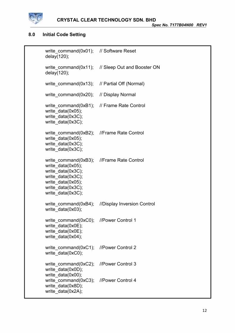
8.0 Initial Code Setting
write_command(0x01); // Software Reset delay(120); write_command(0x11); // Sleep Out and Booster ON delay(120);
write_command(0x13); // Partial Off (Normal) write_command(0x20); // Display Normal
write_command(0xB1); // Frame Rate Control write_data(0x05); write_data(0x3C); write_data(0x3C); write_command(0xB2); //Frame Rate Control write_data(0x05); write_data(0x3C); write_data(0x3C); write_command(0xB3); //Frame Rate Control write_data(0x05); write_data(0x3C); write_data(0x3C); write_data(0x05); write_data(0x3C); write_data(0x3C); write_command(0xB4); //Display Inversion Control write_data(0x03); write_command(0xC0); //Power Control 1 write_data(0x0E); write_data(0x0E); write_data(0x04); write_command(0xC1); //Power Control 2 write_data(0xC0); write_command(0xC2); //Power Control 3 write_data(0x0D); write_data(0x00); write_command(0xC3); //Power Control 4 write_data(0x8D); write_data(0x2A);

CRYSTAL CLEAR TECHNOLOGY SDN. BHD Spec No. T177B04N00 REV1
13
write_command(0xC4); //Power Control 5 write_data(0x8D); write_data(0xEE); write_command(0xC5); //VCOM Control 1 write_data(0x0C); write_command(0x36); //Memory Data Access Control write_data(0xD0); write_command(0xE0); //Gamma Adjustment write_data(0x0C); write_data(0x1C); write_data(0x0F); write_data(0x18); write_data(0x36); write_data(0x2F); write_data(0x27); write_data(0x2A); write_data(0x27); write_data(0x25); write_data(0x2D); write_data(0x3C); write_data(0x00); write_data(0x05); write_data(0x03); write_data(0x10); write_command(0xE1); //Gamma Adjustment write_data(0x0C); write_data(0x1A); write_data(0x09); write_data(0x09); write_data(0x26); write_data(0x22); write_data(0x1E); write_data(0x25); write_data(0x25); write_data(0x25); write_data(0x2E); write_data(0x3B); write_data(0x00); write_data(0x05); write_data(0x03); write_data(0x10); write_command(0x3A); //Interface Pixel Format write_data(0x05); write_command(0x29); //Display On
CRYSTAL CLEAR TECHNOLOGY SDN. BHD Spec No. T177B04N00 REV1
14
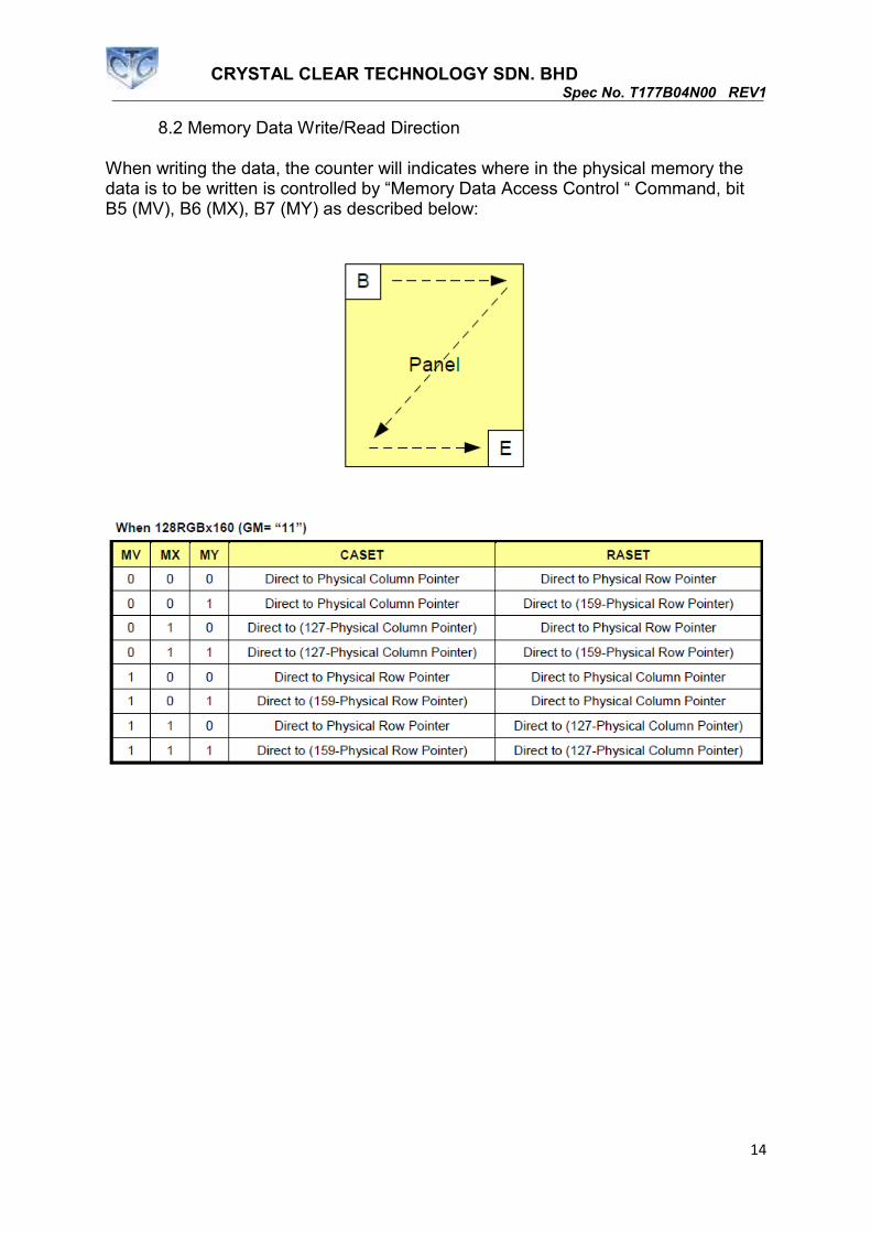
8.2 Memory Data Write/Read Direction When writing the data, the counter will indicates where in the physical memory the data is to be written is controlled by “Memory Data Access Control “ Command, bit B5 (MV), B6 (MX), B7 (MY) as described below:

CRYSTAL CLEAR TECHNOLOGY SDN. BHD Spec No. T177B04N00 REV1
15
9.0 Reliability Test Condition
Item Test Condition
Operating
High Temperature 70degC, 96 hrs
Low Temperature -20degC,96 hrs
Storage
High Temperature 8degC, 240hrs and recovery for 2hrs
Low Temperature -30degC, 240hrs and recovery for 2hrs
High Temperature and High Humidity
50degC, 90%RH, 240hrs and recovery for 2 hrs
Thermal
Cycle Rt � -30degV � Rt � 80degC � RT 0min 30min 5min 30min 5min 50 cycles (Power off)
Shock Rt � -30degV � 80degC 0min 30min 30min 50 cycles (Power off)
Note: Rt means Room temperature

CRYSTAL CLEAR TECHNOLOGY SDN. BHD Spec No. T177B04N00 REV1
16
10.0 Inspection Criteria No Defect Definition of defect Inspection Criteria
1
a) Definition of dot
The size of defective dot over ½ of whole is regards as one defective dot. Smaller than ½ Larger than ½
‘No dot defect’ ‘1 dot defect’ (ignore) (counted)
A – Viewing Area B – Outside viewing area
b) Bright Dot Dot appear bright and unchanged in size when LCD panel is displaying black pattern Defect A B
Bright Dot 1
NC Dark Dot 2
Total 3
NC – Not Count c) Dark Dot
Dot appear dark and unchanged in size when LCD panel is displaying pure color (RED, GREEN or BLUE) pattern
d) 2 dot adjacent
1 pair = 2 dots
Type 1 Type 2
or
Type 3
Defect Acc. Count
2 Bright dot Adjacent 0
2 Dark dot Adjacent 1
2
Black spot White Spot Bright spot Pin Hole Foreign Particle
-Black/Dark/Bright Spot is points on display which appear dark/bright and usually result from contamination - These defect do not vary in size intensity (contrast) when contras is varied.
Defect Category A B
D ≤ 0.10 NC
NC 0.10 ≤ D ≤ 0.15 2
0.15 ≤ D ≤ 0.20 1
D ≥ 0.2 0
3
Black Line White line Particle between POL and Glass Scratch on Glass
Defect Category A B
W ≤ 0.03 NC
NC 0.03 ≤ W ≤ 0.05, L ≤2.0 2
W ≥ 0.05 0
4 POL Bubble POL Dented
Defect Category A B
D ≤ 0.20 NC
NC 0.20 ≤ D ≤ 0.30 3
0.30 ≤ D ≤ 0.50 2
D ≥ 0.5 0
5 Mura (50% Grey)
Judged by Limit sample

CRYSTAL CLEAR TECHNOLOGY SDN. BHD Spec No. T177B04N00 REV1
17
11.0 Precaution and Limited Warranty
1. Handing Precautions a. The display panel is made of glass and polarizer. As glass is fragile. It tends to chip
during handling especially on the edges. Please avoid dropping or jarring. Do not subject it to a mechanical shock of impact or by dropping it.
b. If the display panel is damaged and the liquid crystal substance leaks out, be sure not to get any in your mouth. If the substance is in contact with your skin or clothes, wash it off using soap and water.
c. Do not apply excessive force to the display surface or the adjoining areas since this may cause the color tone to vary. Do not touch the display with bare hands. This will stain the display area and degrade the insulation between terminals. Scratch and dents may occur on polarizer too.
d. The polarizer covering the display surface of the LCD module is soft and easily scratched. Handle this polarizer carefully. Do not touch, push or rub the exposed polarizers with anything harder than a HB pencil lead (glass, tweezers, etc.). Do not put or attach anything on the display area to avoid leaving marks on it. Condensation on the surface and contact with terminals due to cold will damage, stain or dirty the polarizer. After products are tested at low temperature they must be warmed up in a container before coming in to contact with room temperature air.
e. If the display surface becomes contaminated, breathe on the surface and gently wipe it with a soft dry cloth. If it is heavily contaminated, moisten cloth with one of the following solvents
- Isopropyl alcohol - Ethyl alcohol - Do not scrub hard to avoid damaging the display surface.
f. Solvents other than those above-mentioned may damage the polarizer. Especially, do not use the following.
- Water - Ketone - Aromatic solvents - Wipe off saliva or water drops immediately, contact with water over a long
period of time may cause deformation or color fading. Avoid contact with oil and fats.
g. Exercise care to minimize corrosion of the electrode. Corrosion of the electrodes is accelerated by water droplets, moisture condensation or a current flow in a high-humidity environment.
h. Install the LCD Module by using the mounting holes. When mounting the LCD module make sure it is free of twisting, warping and distortion. In particular, do not forcibly pull or bend the I/O cable or the backlight cable.
i. Do not attempt to disassemble or process the LCD module. j. NC terminal should be open. Do not connect anything. k. If the logic circuit power is off, do not apply the input signals. l. Electro-Static Discharge Control. Since this module uses a CMOS LSI, the same
careful attention should be paid to electrostatic discharge as for an ordinary CMOS IC. To prevent destruction of the elements by static electricity, be careful to maintain an optimum work environment.
- Before removing LCM from its packing case or incorporating it into a set, be sure the module and your body have the same electric potential. Be sure to ground the body when handling the LCD modules.
- Tools required for assembly, such as soldering irons, must be properly grounded. Make certain the AC power source for the soldering iron does not leak. When using an electric screwdriver to attach LCM, the screw driver should be of ground potentiality to minimize as much as possible any

CRYSTAL CLEAR TECHNOLOGY SDN. BHD Spec No. T177B04N00 REV1
18
transmission of electromagnetic waves produced sparks coming from the commutator of the motor.
- To reduce the amount of static electricity generated, do not conduct assembly and other work under dry conditions. To reduce the generation of static electricity be careful that the air in the work environment is not too dry. A relative humidity of 50%-60% is recommended. As far as possible make the electric potential of your work clothes and that of the work bench the ground potential.
- The LCD module is coated with a film to protect the display surface. Exercise care when peeling off this protective film since static electricity may be generated.
m. Since LCM has been assembled and adjusted with a high degree of precision, avoid applying excessive shocks to the module or making any alterations or modifications to it.
- Do not alter, modify or change the shape of the tab on the metal frame. - Do not make extra holes on the printed circuit board, modify its shape or
change the positions of components to be attached. - Do not damage or modify the pattern writing on the printed circuit board. - Absolutely do not modify the zebra rubber strip (conductive rubber) or heat
seal connector. - Except for soldering the interface, do not make any alterations or
modifications with a soldering iron. - Do not drop, bend or twist the LCM.
2. Storage Precautions
When storing the LCD modules, the following precaution are necessary. a. Store them in a sealed polyethylene bag. If properly sealed, there is no need for
the desiccant. b. Store them in a dark place. Do not expose to sunlight or fluorescent light, keep
the temperature between 0C and 35C, and keep the relative humidity between 40%RH and 60%RH.
c. The polarizer surface should not come in contact with any other objects. 3. Others
a. Liquid crystals solidify under low temperature (below the storage temperature range) leading to defective orientation or the generation of air bubbles (black or white). Air bubbles may also be generated if the module is subject to a low temperature.
b. If the LCD modules have been operating for a long time showing the same display patterns, the display patterns may remain on the screen as ghost images and a slight contrast irregularity may also appear. A normal operating status can be regained by suspending use for some time. It should be noted that this phenomenon does not adversely affect performance reliability.
c. To minimize the performance degradation of the LCD modules resulting from destruction caused by static electricity etc. Exercise care to avoid holding the following sections when handling the modules.
Exposed area of the printed circuit board. Terminal electrode sections.
4. Using LCD Modules a. Installing LCD Modules
The hole in the printed circuit board is used to fix LCM as shown in the picture below. Attend to the following items when installing the LCM.
b. Cover the surface with a transparent protective plate to protect the polarizer and LC cell.

CRYSTAL CLEAR TECHNOLOGY SDN. BHD Spec No. T177B04N00 REV1
19
c. When assembling the LCM into other equipment, the spacer to the bit between the LCM and the fitting plate should have enough height to avoid causing stress to the module surface, refer to the individual specifications for measurements. The measurement tolerance should be 0.1mm.
d. Precaution for assemble the module with BTB connector: Please note the position of the male and female connector position, don’t
assemble or assemble like the method which the following picture shows
5. Precaution for soldering the LCM
Manual soldering Machine drag
soldering
Machine press
soldering
No RoHS
Product
290°C ~350°C.
Time: 3-5S.
330°C ~350°C.
Speed: 4-8 mm/s.
300°C ~330°C.
Time: 3-6S.
Press: 0.8~1.2Mpa
RoHS
Product
340°C ~370°C.
Time: 3-5S.
350°C ~370°C.
Time: 4-8 mm/s.
330°C ~360°C.
Time: 3-6S.
Press: 0.8~1.2Mpa
a. If soldering flux is used, be sure to remove any remaining flux after finishing the soldering operation (This does not apply in the case of a non-halogen type of flux). It is recommended that you protect the LCD surface with a cover during soldering to prevent any damage due to flux spatters.
b. When soldering the electroluminescent panel and PC board, the panel and board should not be detached more than three times. This maximum number is determined by the temperature and time conditions mentioned above, though there may be some variance depending on the temperature of the soldering iron.
c. When removing the electroluminescent panel from the PC board, be sure the solder has completely melted, the soldered pad on the PC board could be damaged.

CRYSTAL CLEAR TECHNOLOGY SDN. BHD Spec No. T177B04N00 REV1
20
6. Precautions for Operation a. Viewing angle varies with the change of liquid crystal driving voltage (VLCD).
Adjust VLCD to show the best contrast. b. It is recommended to drive LCD's within the specified voltage limit since over limit
will cause shorter LCD life. An electrochemical reaction due to direct current causes LCD deterioration. Avoid the use of direct current drive.
c. Response time will be extremely delayed at lower temperature compared to room operating temperature range and on the other hand, at higher temperature LCD shows dark color in them. However those phenomena do not mean malfunction. The LCD will return to normal performance when ambient temperature revert to room condition.
d. If the display area is pushed hard during operation, the display will become abnormal. However, it will return to normal if it is turned off and on.
e. A slight dew depositing on terminals is a cause for electro-chemical reaction resulting in terminal open circuit.
f. Input logic voltage before apply analogue high voltage such as LCD driving voltage when power on. Remove analogue high voltage before logic voltage when power off the module. Input each signal after the positive/negative voltage becomes stable.
g. Please keep the temperature within the specified range for use and storage. Polarization degradation, bubble generation or polarizer peel-off may occur with high temperature and high humidity.
7. Safety
a. It is recommended to crush damaged or unnecessary LCDs into pieces and wash them off with solvents such as acetone and ethanol, which should later be burned.
b. If any liquid leaks out of a damaged glass cell and comes in contact with the hands, wash off thoroughly with soap and water.
8. Limited Warranty Unless otherwise agreed between Crystal Clear Technology and customer, Crystal Clear Technology will replace or repair any of its LCD and LCM which is found to be defective electrically and visually when inspected in accordance with Crystal Clear Technology acceptance standards, for a period of one year from date of shipment. Confirmation of such date shall be based on freight documents. The warranty liability of Crystal Clear Technology is limited to repair and/or replacement on the terms set forth above. Crystal Clear Technology will not responsible for any subsequent or consequential events.
9. Return LCM under Warranty
No warranty can be granted if the precautions stated above have been disregarded. The typical examples of violations are: - Broken LCD glass - PCB eyelet’s damaged or modified - PCB conductors damaged - Circuit modified in any way, including addition of components. - PCB tampered with by grinding, engraving or painting varnish. - Soldering to, or modifying the bezel in any manner. Module repairs will be invoiced to customer upon mutual agreement. Modules must be returned with sufficient description of failure or defects. Any connectors or cable installed by customer must be removed completely without damaging the PCB eyelet’s, conductors and terminals.
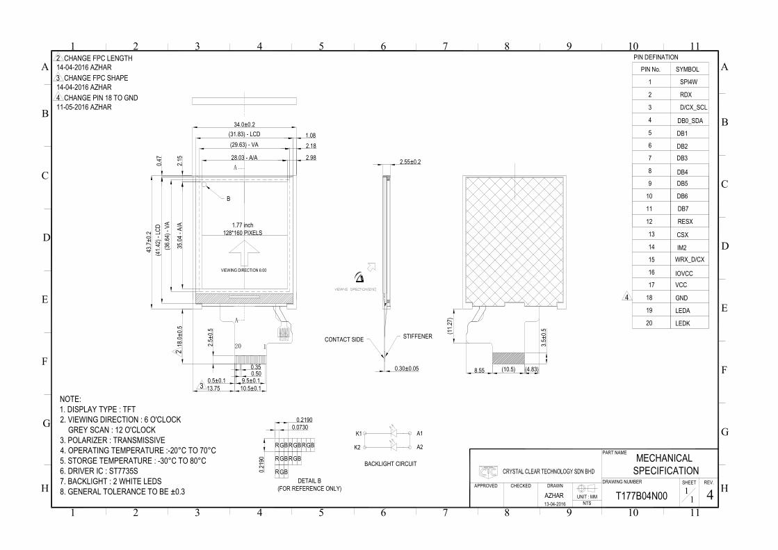
K2
K1
A2
A1
2.1
5
43.7
±0
.2
35.0
4 -
A/A
34.0±0.2
28.03 - A/A
(31.83) - LCD
(41.
42)
- LC
D
0.30±0.05
2.55±0.2A
A
VIEWING DIRECTION 6:00
1.77 inch
128*160 PIXELS
1.08
2.18
2.980.
47
B
(29.63) - VA
CONTACT SIDE
DETAIL B
(FOR REFERENCE ONLY)
0.07300.2190
0.2
190
R GB R GB R GB
R GBR GB
R GB
BACKLIGHT CIRCUIT
NOTE:
1. DISPLAY TYPE : TFT
2. VIEWING DIRECTION : 6 O'CLOCK
GREY SCAN : 12 O'CLOCK
3. POLARIZER : TRANSMISSIVE
4. OPERATING TEMPERATURE :-20°C TO 70°C
5. STORGE TEMPERATURE : -30°C TO 80°C
6. DRIVER IC : ST7735S
7. BACKLIGHT : 2 WHITE LEDS
8. GENERAL TOLERANCE TO BE ±0.3
(36.
64)
- V
A
H
1 2 3 4 5 6
G
F
E
C
D
B
A
1 2 3 4 5 6
PART NAME
DRAWING NUMBERCHECKED
7 8
APPROVED
AZHAR
13-04-2016 NTS
UNIT : MM
9
DRAWNSHEET
MECHANICAL
SPECIFICATION
T177B04N00
10
H41
1
11
REV.
G
F
E
C
D
B
7 8 9 10
A
11
20 1
A1 A2 K2 K1
0.350.50
9.5±0.1
10.5±0.1
0.5±0.1
2.5±
0.5
3.5
±0.
5
13.75
(10.5)8.55
(11
.27)
(4.83)
RDX
SPI4W
RESX
DB7
DB6
DB5
12
11
10
9
8
7
D/CX_SCL
6
5
4
3
2
PIN No. SYMBOL
1
PIN DEFINATION
DB4
DB3
DB2
DB1
DB0_SDA
VCC
20
19
18
17
16
15
14
13
IOVCC
WRX_D/CX
IM2
CSX
LEDK
LEDA
GND
STIFFENER
18.
0±0.
52
3
4
2 CHANGE FPC LENGTH
14-04-2016 AZHAR
3 CHANGE FPC SHAPE
14-04-2016 AZHAR
4 CHANGE PIN 18 TO GND
11-05-2016 AZHAR