Embed Size (px)
Citation preview
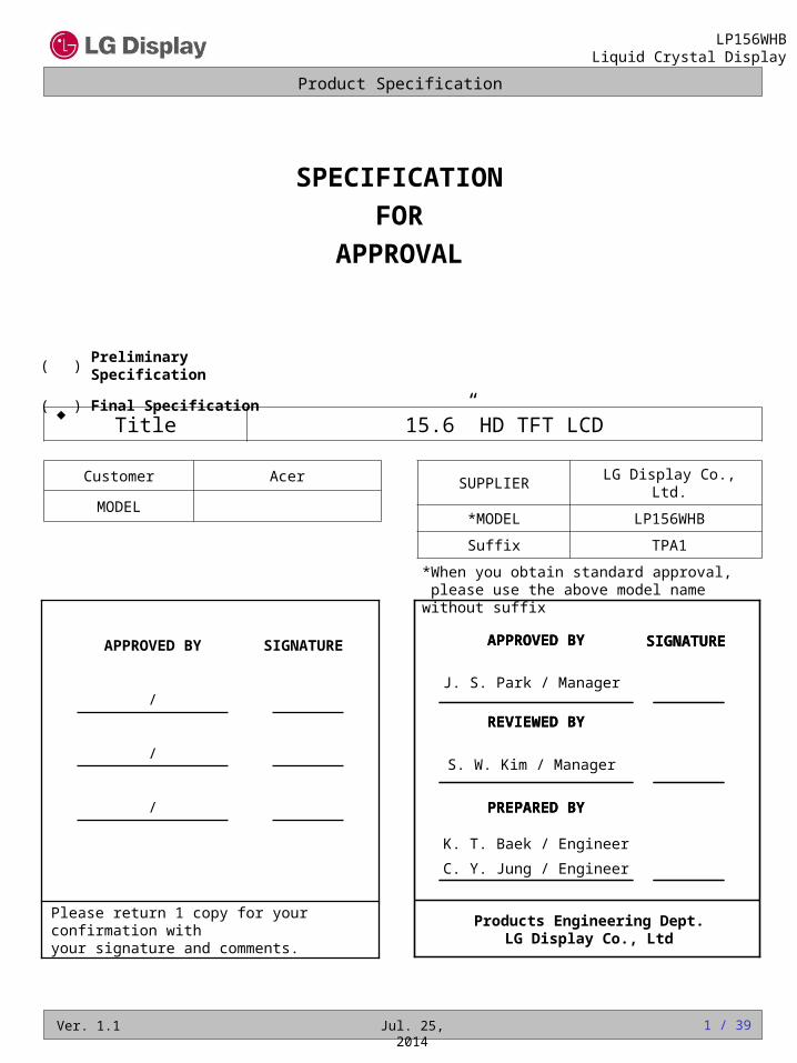
Product Specification
LP156WHBLiquid Crystal Display
Ver. 1.1 Jul. 25, 2014 1 / 39
SPECIFICATION
FOR
APPROVAL
Title 15.6” HD TFT LCD
Customer Acer
MODEL
SUPPLIER LG Display Co., Ltd.
*MODEL LP156WHB
Suffix TPA1
*When you obtain standard approval, please use the above model name without suffix
( ) Preliminary Specification
( ) Final Specification
Please return 1 copy for your confirmation withyour signature and comments.
/
/
/
SIGNATUREAPPROVED BY
Products Engineering Dept.LG Display Co., Ltd
PREPARED BY
REVIEWED BY
SIGNATUREAPPROVED BY
PREPARED BY
REVIEWED BY
SIGNATUREAPPROVED BY
S. W. Kim / Manager
K. T. Baek / Engineer
C. Y. Jung / Engineer
J. S. Park / Manager
Product Specification
LP156WHBLiquid Crystal Display
Ver. 1.1 Jul. 25, 2014 2 / 39
Contents
RECORD OF REVISIONS…………………………………………………………………… 3
1. GENERAL DESCRIPTION……………………………………………………………… 4
2. ABSOLUTE MAXIMUM
RATINGS……………………………………………………...5
3. ELECTRICAL SPECIFICATIONS………………………………………….
……………6
3-1. LCD ELECTRICAL CHARACTREISTICS…..…………………………………………..... 6
3-2. LED BACKLIGHT ELECTRICAL CHARACTREISTICS………………………………..... 6
3-3. INTERFACE CONNECTIONS……………………………………………………………… 8
3-4. LVDS SIGNAL TIMING SPECIFICATION………………………………………………… 9
3-5. SIGNAL TIMING SPECIFICATIONS………………………………………………………. 11
3-6. SIGNAL TIMING WAVEFORMS…………………………………………………………… 11
3-7. COLOR INPUT DATA REFERENCE……………………………………………………… 12
3-8. POWER SEQUENCE……………………………………………………………………….. 13
4. OPTICAL SPECIFICATIONS……………………………………………………………1
4
5. MECHANICAL CHARACTERISTICS………………………………………………….1
7
6. RELIABLITY………………………………………………………………………………2
5
7. INTERNATIONAL STANDARDS……………………………………………………….2
6
7-1. SAFETY…………………………………………………………………..………………...… 26
7-2. ENVIRONMENT……………………………………………………………..…………...…. 26
8. PACKING………………………………………………………………………...………..2
7
8-1. DESIGNATION OF LOT MARK………………………………………………….………… 27
8-2. PACKING FORM…………………………………………………………………..………… 27
9.PRECAUTIONS…………………………………………………………………………
…
2
8
APPENDIX A. LGD PROPOSAL FOR SYSTEM COVER DESIGN………………...……………..……. 20
APPENDIX B. LGD PROPOSAL FOR eDP INTERFACE DESIGN GUIDE…………….………………. 20
APPENDIX C. ENHANCED EXTENDED DISPLAY IDENTIFICAION DATA….…………………….….. 30
Product Specification
LP156WHBLiquid Crystal Display
Ver. 1.1 Jul. 25, 2014 3 / 39
Record of Revisions
Revision No Revision Date Page DescriptionEDID
version
0.0 Dec. 06. 2013 All First Draft (Preliminary Specification) 0.0
0.1 Mar. 17. 2014 4,6,7 Power Consumption Update
14 Color Coordinates Update
31~33 EDID Update 1.0
1.0 May. 07. 2014 - Final Version -
1.1 Jul. 25. 2014 24 Packing update
Product Specification
LP156WHBLiquid Crystal Display
Ver. 1.1 Jul. 25, 2014
1. General Description
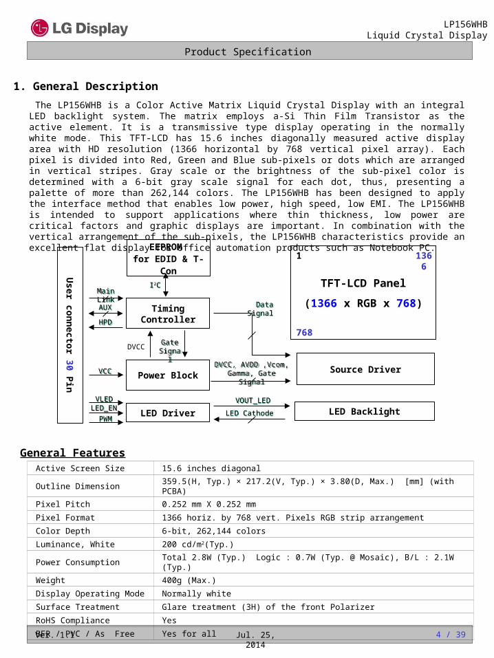
The LP156WHB is a Color Active Matrix Liquid Crystal Display with an integral LED backlight system. The matrix employs a-Si Thin Film Transistor as the active element. It is a transmissive type display operating in the normally white mode. This TFT-LCD has 15.6 inches diagonally measured active display area with HD resolution (1366 horizontal by 768 vertical pixel array). Each pixel is divided into Red, Green and Blue sub-pixels or dots which are arranged in vertical stripes. Gray scale or the brightness of the sub-pixel color is determined with a 6-bit gray scale signal for each dot, thus, presenting a palette of more than 262,144 colors. The LP156WHB has been designed to apply the interface method that enables low power, high speed, low EMI. The LP156WHB is intended to support applications where thin thickness, low power are critical factors and graphic displays are important. In combination with the vertical arrangement of the sub-pixels, the LP156WHB characteristics provide an excellent flat display for office automation products such as Notebook PC.
VLEDVLEDLED_ENLED_EN
PWMPWM
VCCVCC
Main LinkMain Link
DVCC, AVDD ,Vcom, Gamma, Gate Signal
DVCC, AVDD ,Vcom, Gamma, Gate Signal
Data SignalData Signal
GateSignalGate
Signal
AUXAUX
HPDHPD
VOUT_LEDVOUT_LED
LED CathodeLED Cathode
General FeaturesActive Screen Size 15.6 inches diagonal
Outline Dimension 359.5(H, Typ.) × 217.2(V, Typ.) × 3.80(D, Max.) [mm] (with PCBA)
Pixel Pitch 0.252 mm X 0.252 mm
Pixel Format 1366 horiz. by 768 vert. Pixels RGB strip arrangement
Color Depth 6-bit, 262,144 colors
Luminance, White 200 cd/m2(Typ.)
Power Consumption Total 2.8W (Typ.) Logic : 0.7W (Typ. @ Mosaic), B/L : 2.1W (Typ.)
Weight 400g (Max.)
Display Operating Mode Normally white
Surface Treatment Glare treatment (3H) of the front Polarizer
RoHS Compliance Yes
BFR / PVC / As Free Yes for all
DVCC
Source Driver
TFT-LCD Panel
(1366 x RGB x 768)
EEPROM for EDID & T-Con
LED Driver
Power Block
TimingController
User co
nn
ector 30 P
inLED Backlight
I2CI2C
1
768
13661
4 / 39
Product Specification
LP156WHBLiquid Crystal Display
Ver. 1.1 Jul. 25, 2014 5 / 39
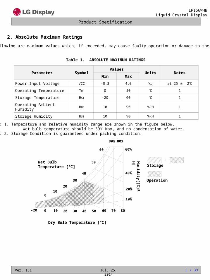
2. Absolute Maximum Ratings
The following are maximum values which, if exceeded, may cause faulty operation or damage to the unit.
Table 1. ABSOLUTE MAXIMUM RATINGS
Storage
Operation
10 20 30 40 50 60 70 800-20
Dry Bulb Temperature [ ]
10%
20%
40%
60%
90% 80%
010
20
30
40
50
60
Wet BulbTemperature [ ]
Hu
mid
ity[(%)R
H]
Note : 1. Temperature and relative humidity range are shown in the figure below. Wet bulb temperature should be 39C Max, and no condensation of water.Note : 2. Storage Condition is guaranteed under packing condition.
Parameter SymbolValues
Units NotesMin Max
Power Input Voltage VCC -0.3 4.0 VDC at 25 2C
Operating Temperature TOP 0 50 C 1
Storage Temperature HST -20 60 C 1
Operating Ambient Humidity HOP 10 90 %RH 1
Storage Humidity HST 10 90 %RH 1
Product Specification
LP156WHBLiquid Crystal Display
Ver. 1.1 Jul. 25, 2014 6 / 39
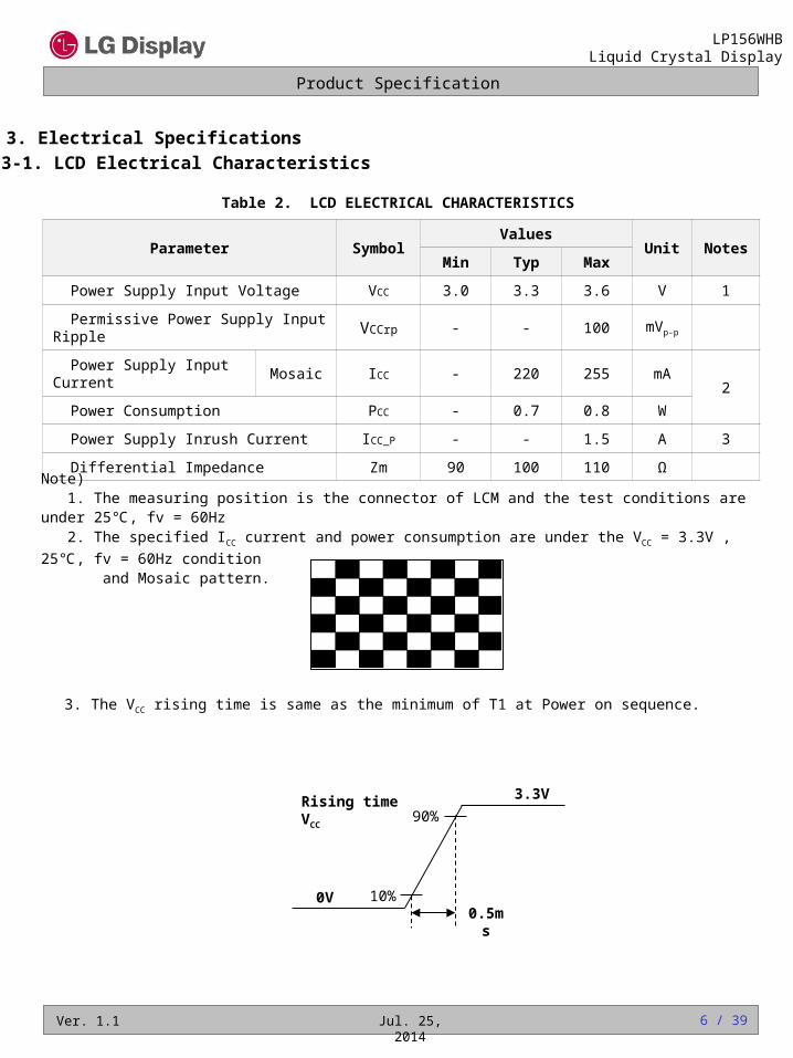
3. Electrical Specifications
3-1. LCD Electrical Characteristics
Table 2. LCD ELECTRICAL CHARACTERISTICS
Parameter SymbolValues
Unit NotesMin Typ Max
Power Supply Input Voltage VCC 3.0 3.3 3.6 V 1
Permissive Power Supply Input Ripple VCCrp - - 100 mVp-p
Power Supply Input Current Mosaic ICC - 220 255 mA2
Power Consumption PCC - 0.7 0.8 W
Power Supply Inrush Current ICC_P - - 1.5 A 3
Differential Impedance Zm 90 100 110 Ω
Note) 1. The measuring position is the connector of LCM and the test conditions are under 25 , fv = 60Hz 2. The specified ICC current and power consumption are under the VCC = 3.3V , 25 , fv = 60Hz condition
and Mosaic pattern.
3. The VCC rising time is same as the minimum of T1 at Power on sequence.
10%
90%
0.5ms
3.3V
0V
Rising timeVCC
Product Specification
LP156WHBLiquid Crystal Display
Ver. 1.1 Jul. 25, 2014 7 / 39
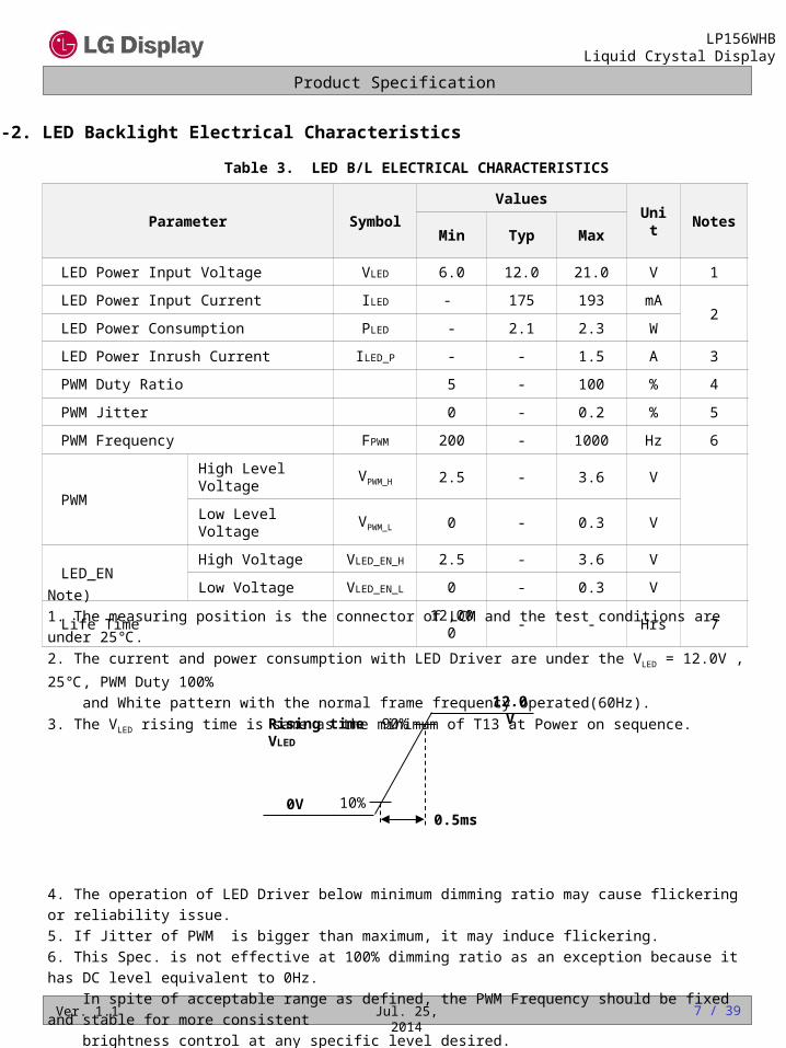
3-2. LED Backlight Electrical Characteristics
Table 3. LED B/L ELECTRICAL CHARACTERISTICS
Parameter SymbolValues
Unit NotesMin Typ Max
LED Power Input Voltage VLED 6.0 12.0 21.0 V 1
LED Power Input Current ILED - 175 193 mA2
LED Power Consumption PLED - 2.1 2.3 W
LED Power Inrush Current ILED_P - - 1.5 A 3
PWM Duty Ratio 5 - 100 % 4
PWM Jitter 0 - 0.2 % 5
PWM Frequency FPWM 200 - 1000 Hz 6
PWMHigh Level Voltage VPWM_H 2.5 - 3.6 V
Low Level Voltage VPWM_L 0 - 0.3 V
LED_ENHigh Voltage VLED_EN_H 2.5 - 3.6 V
Low Voltage VLED_EN_L 0 - 0.3 V
Life Time 12,000 - - Hrs 7
Note)
1. The measuring position is the connector of LCM and the test conditions are under 25 .
2. The current and power consumption with LED Driver are under the VLED = 12.0V , 25 , PWM Duty 100%
and White pattern with the normal frame frequency operated(60Hz).
3. The VLED rising time is same as the minimum of T13 at Power on sequence.
4. The operation of LED Driver below minimum dimming ratio may cause flickering or reliability issue.
5. If Jitter of PWM is bigger than maximum, it may induce flickering.
6. This Spec. is not effective at 100% dimming ratio as an exception because it has DC level equivalent to 0Hz.
In spite of acceptable range as defined, the PWM Frequency should be fixed and stable for more consistent
brightness control at any specific level desired.
7. The life time is determined as the time at which brightness of LCD is 50% compare to that of minimum
value specified in table 7. under general user condition.
10%
90%
0.5ms
12.0V
0V
Rising timeVLED
Product Specification
LP156WHBLiquid Crystal Display
Ver. 1.1 Jul. 25, 2014 8 / 39
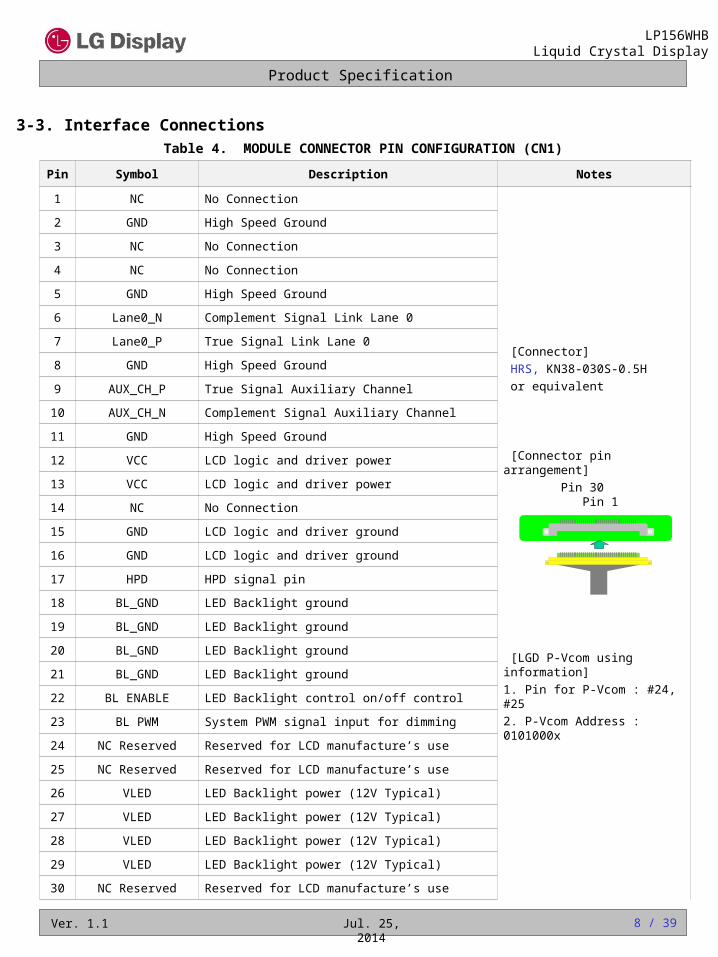
3-3. Interface Connections
Table 4. MODULE CONNECTOR PIN CONFIGURATION (CN1)
Pin Symbol Description Notes
1 NC No Connection
[Connector]
HRS, KN38-030S-0.5H
or equivalent
[Connector pin arrangement]
Pin 30 Pin 1
[LGD P-Vcom using information]
1. Pin for P-Vcom : #24, #25
2. P-Vcom Address : 0101000x
2 GND High Speed Ground
3 NC No Connection
4 NC No Connection
5 GND High Speed Ground
6 Lane0_N Complement Signal Link Lane 0
7 Lane0_P True Signal Link Lane 0
8 GND High Speed Ground
9 AUX_CH_P True Signal Auxiliary Channel
10 AUX_CH_N Complement Signal Auxiliary Channel
11 GND High Speed Ground
12 VCC LCD logic and driver power
13 VCC LCD logic and driver power
14 NC No Connection
15 GND LCD logic and driver ground
16 GND LCD logic and driver ground
17 HPD HPD signal pin
18 BL_GND LED Backlight ground
19 BL_GND LED Backlight ground
20 BL_GND LED Backlight ground
21 BL_GND LED Backlight ground
22 BL ENABLE LED Backlight control on/off control
23 BL PWM System PWM signal input for dimming
24 NC Reserved Reserved for LCD manufacture’s use
25 NC Reserved Reserved for LCD manufacture’s use
26 VLED LED Backlight power (12V Typical)
27 VLED LED Backlight power (12V Typical)
28 VLED LED Backlight power (12V Typical)
29 VLED LED Backlight power (12V Typical)
30 NC Reserved Reserved for LCD manufacture’s use
Product Specification
LP156WHBLiquid Crystal Display
Ver. 1.1 Jul. 25, 2014
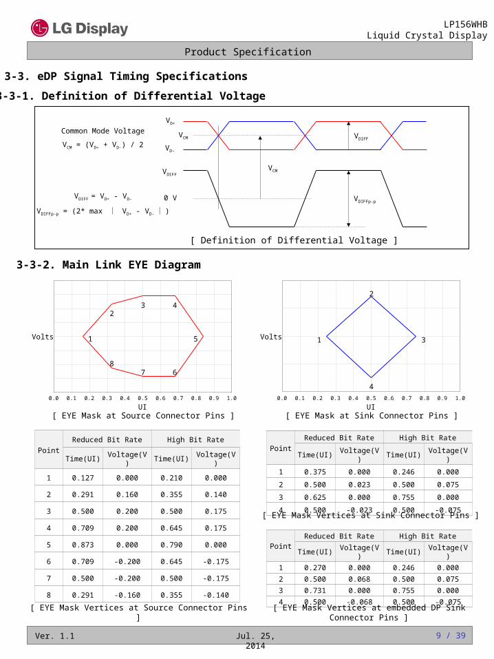
3-3-2. Main Link EYE Diagram
3-3. eDP Signal Timing Specifications
VDIFFp-p
VDIFF
VCM
VD+
VD-
VDIFF
0 VVDIFF = VD+ - VD-
VDIFFp-p = (2* max | VD+ - VD- | )
Common Mode Voltage
VCM = (VD+ + VD-) / 2VCM
[ Definition of Differential Voltage ]
UI
Volts
0.0 0.1 0.2 0.3 0.4 0.5 0.6 0.7 0.8 0.9 1.0
1
23 4
5
678
UI
Volts
0.0 0.1 0.2 0.3 0.4 0.5 0.6 0.7 0.8 0.9 1.0
1
2
3
4
[ EYE Mask at Source Connector Pins ] [ EYE Mask at Sink Connector Pins ]
PointReduced Bit Rate High Bit Rate
Time(UI) Voltage(V) Time(UI) Voltage(V)
1 0.127 0.000 0.210 0.000
2 0.291 0.160 0.355 0.140
3 0.500 0.200 0.500 0.175
4 0.709 0.200 0.645 0.175
5 0.873 0.000 0.790 0.000
6 0.709 -0.200 0.645 -0.175
7 0.500 -0.200 0.500 -0.175
8 0.291 -0.160 0.355 -0.140
PointReduced Bit Rate High Bit Rate
Time(UI) Voltage(V) Time(UI) Voltage(V)
1 0.375 0.000 0.246 0.000
2 0.500 0.023 0.500 0.075
3 0.625 0.000 0.755 0.000
4 0.500 -0.023 0.500 -0.075
[ EYE Mask Vertices at Source Connector Pins ]
[ EYE Mask Vertices at Sink Connector Pins ]
PointReduced Bit Rate High Bit Rate
Time(UI) Voltage(V) Time(UI) Voltage(V)
1 0.270 0.000 0.246 0.000
2 0.500 0.068 0.500 0.075
3 0.731 0.000 0.755 0.000
4 0.500 -0.068 0.500 -0.075
[ EYE Mask Vertices at embedded DP Sink Connector Pins ]
3-3-1. Definition of Differential Voltage
9 / 39
Product Specification
LP156WHBLiquid Crystal Display
Ver. 1.1 Jul. 25, 2014
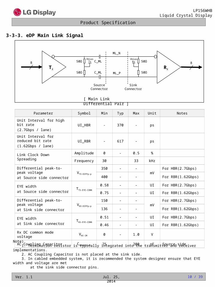
Parameter Symbol Min Typ Max Unit Notes
Unit Interval for high bit rate
(2.7Gbps / lane)UI_HBR - 370 - ps
Unit Interval for reduced bit rate
(1.62Gbps / lane)UI_RBR - 617 - ps
Link Clock Down SpreadingAmplitude 0 - 0.5 %
Frequency 30 33 kHz
Differential peak-to-peak voltage
at Source side connectorVTX-DIFFp-p
350 - -mV
For HBR(2.7Gbps)
400 - - For RBR(1.62Gbps)
EYE width
at Source side connectorTTX-EYE-CONN
0.58 - - UI For HBR(2.7Gbps)
0.75 - - UI For RBR(1.62Gbps)
Differential peak-to-peak voltage
at Sink side connectorVRX-DIFFp-p
150 - -mV
For HBR(2.7Gbps)
136 - - For RBR(1.62Gbps)
EYE width
at Sink side connectorTRX-EYE-CONN
0.51 - - UI For HBR(2.7Gbps)
0.46 - - UI For RBR(1.62Gbps)
Rx DC common mode voltage VRX CM 0 - 1.0 V
AC Coupling Capacitor CSOURCE_ML 75 200 nF Source side
3-3-3. eDP Main Link Signal
Note) 1. Termination resistor is typically integrated into the transmitter and receiver implementations. 2. AC Coupling Capacitor is not placed at the sink side. 3. In cabled embedded system, it is recommended the system designer ensure that EYE width and voltage are met at the sink side connector pins.
10 / 39
50Ω
50Ω
50Ω
50Ω
VbiasTx
VbiasRxC_ML
C_ML
SourceConnector
SinkConnector
8 8
ML_N
ML_P
[ Main Link Differential Pair ]
TX RX
Product Specification
LP156WHBLiquid Crystal Display
Ver. 1.1 Jul. 25, 2014
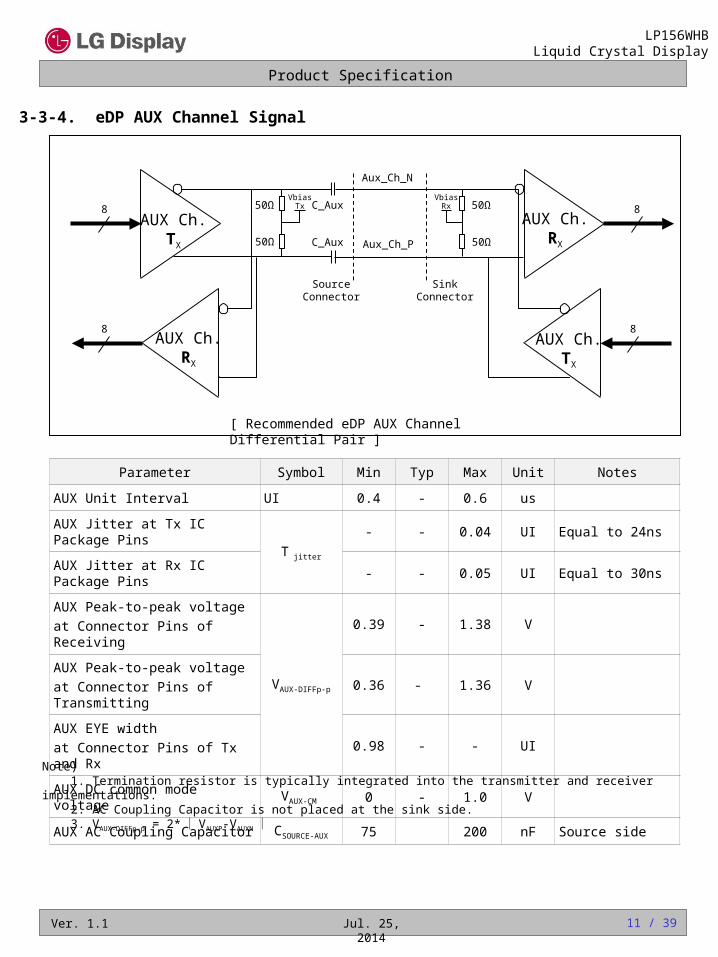
3-3-4. eDP AUX Channel Signal
Parameter Symbol Min Typ Max Unit Notes
AUX Unit Interval UI 0.4 - 0.6 us
AUX Jitter at Tx IC Package PinsT jitter
- - 0.04 UI Equal to 24ns
AUX Jitter at Rx IC Package Pins - - 0.05 UI Equal to 30ns
AUX Peak-to-peak voltage
at Connector Pins of Receiving
VAUX-DIFFp-p
0.39 - 1.38 V
AUX Peak-to-peak voltage
at Connector Pins of Transmitting0.36 - 1.36 V
AUX EYE width
at Connector Pins of Tx and Rx0.98 - - UI
AUX DC common mode voltage VAUX-CM 0 - 1.0 V
AUX AC Coupling Capacitor CSOURCE-AUX 75 200 nF Source side
Note) 1. Termination resistor is typically integrated into the transmitter and receiver implementations. 2. AC Coupling Capacitor is not placed at the sink side. 3. VAUX-DIFFp-p = 2* | VAUXP-VAUXN |
11 / 39
50Ω
50Ω
50Ω
50Ω
VbiasTx
VbiasRxC_Aux
C_Aux
SourceConnector
SinkConnector
8 8
8 8
Aux_Ch_N
Aux_Ch_P
[ Recommended eDP AUX Channel Differential Pair ]
AUX Ch.TX
AUX Ch.RX
AUX Ch.TX
AUX Ch.RX
Product Specification
LP156WHBLiquid Crystal Display
Ver. 1.1 Jul. 25, 2014
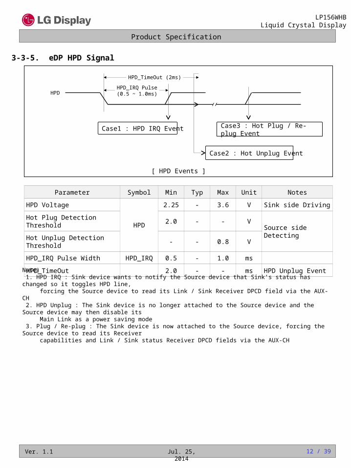
3-3-5. eDP HPD Signal
Parameter Symbol Min Typ Max Unit Notes
HPD Voltage
HPD
2.25 - 3.6 V Sink side Driving
Hot Plug Detection Threshold 2.0 - - VSource side Detecting
Hot Unplug Detection Threshold - - 0.8 V
HPD_IRQ Pulse Width HPD_IRQ 0.5 - 1.0 ms
HPD_TimeOut 2.0 - - ms HPD Unplug Event
[ HPD Events ]
HPD_TimeOut (2ms)
HPD_IRQ Pulse(0.5 ~ 1.0ms)HPD
Case1 : HPD IRQ Event
Case2 : Hot Unplug Event
Case3 : Hot Plug / Re-plug Event
Note) 1. HPD IRQ : Sink device wants to notify the Source device that Sink’s status has changed so it toggles HPD line, forcing the Source device to read its Link / Sink Receiver DPCD field via the AUX-CH 2. HPD Unplug : The Sink device is no longer attached to the Source device and the Source device may then disable its Main Link as a power saving mode 3. Plug / Re-plug : The Sink device is now attached to the Source device, forcing the Source device to read its Receiver capabilities and Link / Sink status Receiver DPCD fields via the AUX-CH
12 / 39
Product Specification
LP156WHBLiquid Crystal Display
Ver. 1.1 Jul. 25, 2014 13 / 39
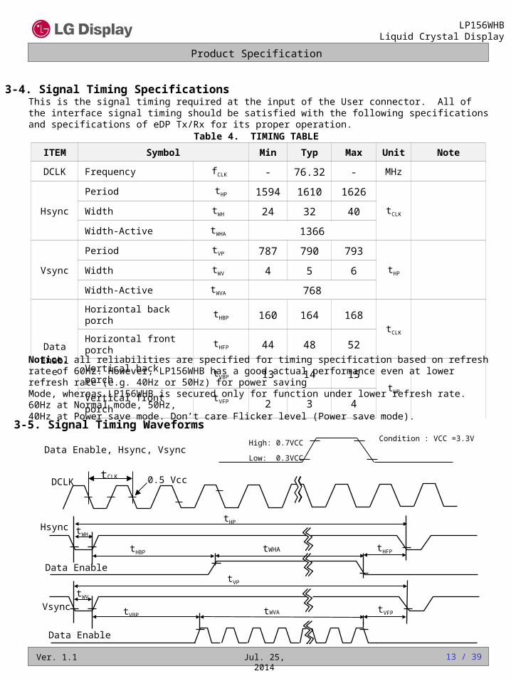
3-4. Signal Timing Specifications
Table 4. TIMING TABLE
This is the signal timing required at the input of the User connector. All of the interface signal timing should be satisfied with the following specifications and specifications of eDP Tx/Rx for its proper operation.
3-5. Signal Timing WaveformsCondition : VCC =3.3V
Low: 0.3VCC
High: 0.7VCCData Enable, Hsync, Vsync
Hsync
Data Enable
Vsync
Data Enable
tWH
tHP
tHFPtHBP
tVP
tWV
tVBPtVFP
tWHA
tWVA
tCLK 0.5 VccDCLK
ITEM Symbol Min Typ Max Unit Note
DCLK Frequency fCLK - 76.32 - MHz
Hsync
Period tHP 1594 1610 1626
tCLKWidth tWH 24 32 40
Width-Active tWHA 1366
Vsync
Period tVP 787 790 793
tHPWidth tWV 4 5 6
Width-Active tWVA 768
Data
Enable
Horizontal back porch tHBP 160 164 168tCLK
Horizontal front porch tHFP 44 48 52
Vertical back porch tVBP 13 14 15tHP
Vertical front porch tVFP 2 3 4Notice. all reliabilities are specified for timing specification based on refresh rate of 60Hz. However, LP156WHB has a good actual performance even at lower refresh rate (e.g. 40Hz or 50Hz) for power savingMode, whereas LP156WHB is secured only for function under lower refresh rate. 60Hz at Normal mode, 50Hz,40Hz at Power save mode. Don’t care Flicker level (Power save mode).
Product Specification
LP156WHBLiquid Crystal Display
Ver. 1.1 Jul. 25, 2014 14 / 39
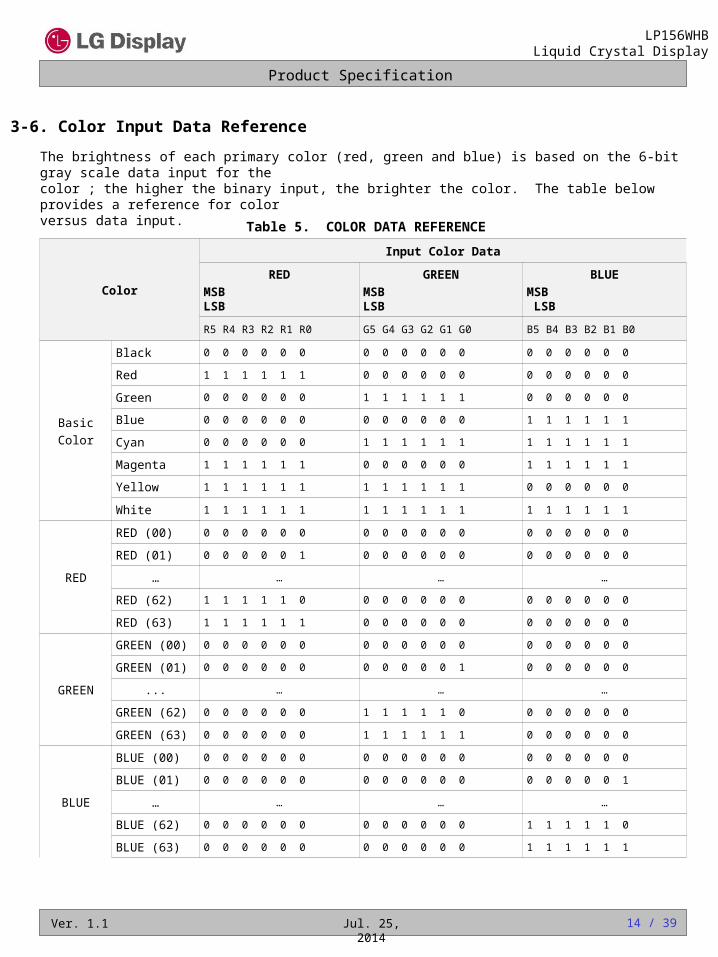
3-6. Color Input Data Reference
The brightness of each primary color (red, green and blue) is based on the 6-bit gray scale data input for thecolor ; the higher the binary input, the brighter the color. The table below provides a reference for color versus data input.
Table 5. COLOR DATA REFERENCE
Color
Input Color Data
RED
MSB LSB
GREEN
MSB LSB
BLUE
MSB LSB
R5 R4 R3 R2 R1 R0 G5 G4 G3 G2 G1 G0 B5 B4 B3 B2 B1 B0
Basic
Color
Black 0 0 0 0 0 0 0 0 0 0 0 0 0 0 0 0 0 0
Red 1 1 1 1 1 1 0 0 0 0 0 0 0 0 0 0 0 0
Green 0 0 0 0 0 0 1 1 1 1 1 1 0 0 0 0 0 0
Blue 0 0 0 0 0 0 0 0 0 0 0 0 1 1 1 1 1 1
Cyan 0 0 0 0 0 0 1 1 1 1 1 1 1 1 1 1 1 1
Magenta 1 1 1 1 1 1 0 0 0 0 0 0 1 1 1 1 1 1
Yellow 1 1 1 1 1 1 1 1 1 1 1 1 0 0 0 0 0 0
White 1 1 1 1 1 1 1 1 1 1 1 1 1 1 1 1 1 1
RED
RED (00) 0 0 0 0 0 0 0 0 0 0 0 0 0 0 0 0 0 0
RED (01) 0 0 0 0 0 1 0 0 0 0 0 0 0 0 0 0 0 0
… … … …
RED (62) 1 1 1 1 1 0 0 0 0 0 0 0 0 0 0 0 0 0
RED (63) 1 1 1 1 1 1 0 0 0 0 0 0 0 0 0 0 0 0
GREEN
GREEN (00) 0 0 0 0 0 0 0 0 0 0 0 0 0 0 0 0 0 0
GREEN (01) 0 0 0 0 0 0 0 0 0 0 0 1 0 0 0 0 0 0
... … … …
GREEN (62) 0 0 0 0 0 0 1 1 1 1 1 0 0 0 0 0 0 0
GREEN (63) 0 0 0 0 0 0 1 1 1 1 1 1 0 0 0 0 0 0
BLUE
BLUE (00) 0 0 0 0 0 0 0 0 0 0 0 0 0 0 0 0 0 0
BLUE (01) 0 0 0 0 0 0 0 0 0 0 0 0 0 0 0 0 0 1
… … … …
BLUE (62) 0 0 0 0 0 0 0 0 0 0 0 0 1 1 1 1 1 0
BLUE (63) 0 0 0 0 0 0 0 0 0 0 0 0 1 1 1 1 1 1
Product Specification
LP156WHBLiquid Crystal Display
Ver. 1.1 Jul. 25, 2014 15 / 39
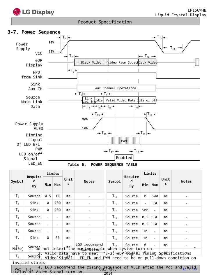
Power Supply VCC
eDPDisplay
HPD from Sink
Sink Aux CH
Source Main Link Data
LED on/off Signal
LED_EN
Dimming signalOf LED B/L
PWM
Power Supply VLED
10%
90%
3-7. Power Sequence
Table 6. POWER SEQUENCE TABLE
Black Video Video From Source Black Video
Aux Channel Operational
Idle or offValid Video DataIdleLink
Training
T10
T1
T2
T11
T3
T4 T7
T5 T6 T8 T9
T12
Enabled
PWM
10%
90%
T13 T14
T16T15
T18T17
Note) 1. Do not insert the mating cable when system turn on. 2. Valid Data have to meet “3-3. eDP Signal Timing Specifications” 3. Video Signal, LED_EN and PWM need to be on pull-down condition on invalid status. 4. LGD recommend the rising sequence of VLED after the Vcc and valid status of Video Signal turn on.
SymbolRequired
By
Limits
Units NotesMin Max
T10 Source 0 500 ms -
T11 Source - 10 ms -
T12 Source 500 - ms
T13 Source 0.5 10 ms -
T14 Source 0.5 10 ms -
T15 Source 10 - ms -
T16 Source 10 - ms -
T17 Source 0 - ms -
T18 Source 0 - ms -
SymbolRequired
By
Limits
Units NotesMin Max
T1 Source 0.5 10 ms -
T2 Sink 0 200 ms -
T3 Sink 0 200 ms -
T4 Source - - ms -
T5 Source - - ms -
T6 Source - - ms -
T7 Sink 0 50 ms -
T8 Source - - msLGD recommend
Min 200ms
T9 Source - - ms -
Product Specification
LP156WHBLiquid Crystal Display
Ver. 1.1 Jul. 25, 2014 16 / 39
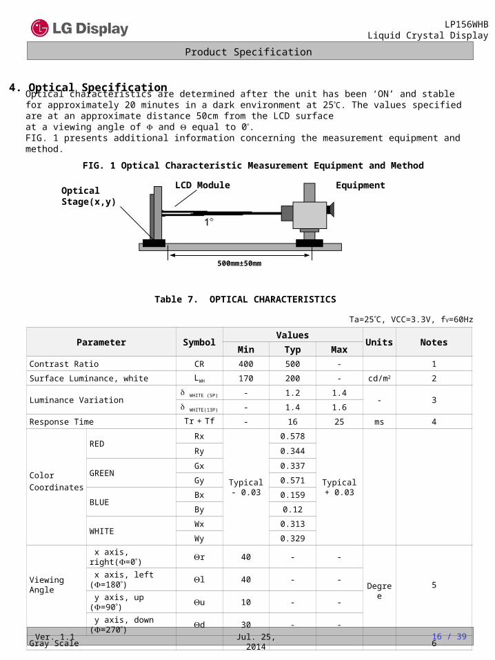
4. Optical Specification
Table 7. OPTICAL CHARACTERISTICS
Ta=25C, VCC=3.3V, fV=60Hz
FIG. 1 Optical Characteristic Measurement Equipment and Method
LCD ModuleOptical Stage(x,y)
Equipment
500mm±50mm
Optical characteristics are determined after the unit has been ‘ON’ and stable for approximately 20 minutes in a dark environment at 25C. The values specified are at an approximate distance 50cm from the LCD surface at a viewing angle of and equal to 0.FIG. 1 presents additional information concerning the measurement equipment and method.
Parameter SymbolValues
Units NotesMin Typ Max
Contrast Ratio CR 400 500 - 1
Surface Luminance, white LWH 170 200 - cd/m2 2
Luminance Variation WHITE (5P) - 1.2 1.4
- 3 WHITE(13P) - 1.4 1.6
Response Time Tr + Tf - 16 25 ms 4
Color
Coordinates
REDRx
Typical- 0.03
0.578
Typical+ 0.03
Ry 0.344
GREENGx 0.337
Gy 0.571
BLUEBx 0.159
By 0.12
WHITEWx 0.313
Wy 0.329
Viewing Angle
x axis, right(=0) r 40 - -
Degree5 x axis, left (=180) l 40 - -
y axis, up (=90) u 10 - -
y axis, down (=270) d 30 - -
Gray Scale 6
Product Specification
LP156WHBLiquid Crystal Display
Ver. 1.1 Jul. 25, 2014 17 / 39
Note) 1. It should be measured in the center of screen(1 Point). Contrast Ratio(CR) is defined mathematically as
Surface Luminance with all white pixels Contrast Ratio(1 Point) = Surface Luminance with all black pixels
2. Surface luminance is the average of 5 point across the LCD surface 50cm from the surface with all pixels displaying white. For more information see FIG 2.
LWH = Average(1,2, … 5 Point)
3. The variation in surface luminance , The panel total variation ( WHITE) is determined by measuring N at each test position 1 through 13 and then defined as following numerical formula. For more information see FIG 2.
Maximum (1,2, … 5 Point) Maximum (1,2, … 13 Point) WHITE (5P) = WHITE (13P) = Minimum (1,2, … 5 Point) Minimum (1,2, … 13 Point)
4. Response time is the time required for the display to transition from white to black (rise time, Tr) and from black to white (falling time, Tf). For additional information see FIG 3.
5. Viewing angle is the angle at which the contrast ratio is greater than 10. The angles are determined for the horizontal or x axis and the vertical or y axis with respect to the z axis which is normal to the LCD surface. For more information see FIG 4.
6. Gray scale specification
Gray Level Luminance [%] (Typ)
L0 0.12
L7 1.12
L15 4.76
L23 11.14
L31 20.11
L39 34.88
L47 52.15
L55 73.50
L63 100
Product Specification
LP156WHBLiquid Crystal Display
Ver. 1.1 Jul. 25, 2014 18 / 39
FIG. 4 Viewing angle
<Dimension of viewing angle range>
Normal
YEye
= 0 ,Right
= 180 ,Left
= 270 ,Down
= 90 , Up
FIG. 3 Response Time
The response time is defined as the following figure and shall be measured by switching the input signal for “black” and “white”.
Tr Tf
10090
100
%
Optical
Response
whiteblack
white
<Measuring point for Average Luminance & measuring point for Luminance variation>
: ACTIVE AREAA : H/4 mmB : V/4 mm
POINTS: 13 POINTS
H,V
Active Area
1
32
54
H
A
B
V
6 7 8
9 10
11 12 13
10mm
10mm
FIG. 2 Luminance
Product Specification
LP156WHBLiquid Crystal Display
Ver. 1.1 Jul. 25, 2014 19 / 39
5. Mechanical CharacteristicsThe contents provide general mechanical characteristics for the model LP156WHB. In addition the figuresin the next page are detailed mechanical drawing of the LCD.
Outline Dimension
Horizontal 359.5 0.5 mm
Vertical 217.2 0.5 mm (with PCBA)
Thickness 3.8 mm (max)
Bezel AreaHorizontal 347.5 0.5 mm
Vertical 196.8 0.5 mm
Active Display AreaHorizontal 344.23 mm
Vertical 193.54 mm
Weight 400g (Max.)
Surface Treatment Hard Coating(3H), Glare treatment of the front polarizer
Product Specification
LP156WHBLiquid Crystal Display
Ver. 1.1 Jul. 25, 2014 20 / 39
<FRONT VIEW> Note) Unit:[mm], General tolerance: 0.5mm
Product Specification
LP156WHBLiquid Crystal Display
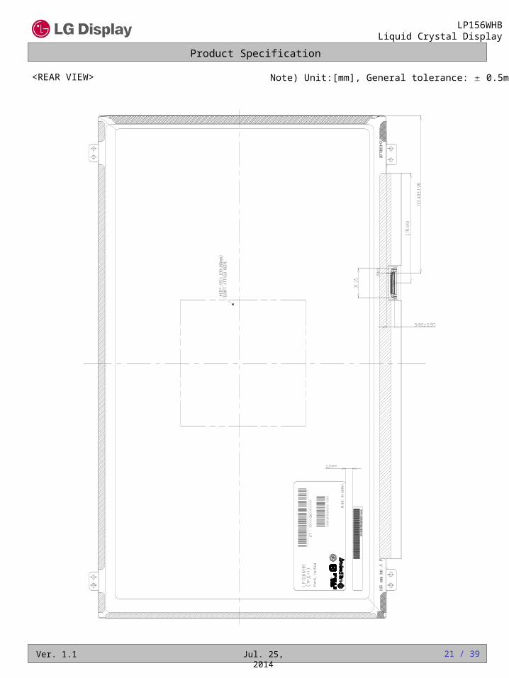
Ver. 1.1 Jul. 25, 2014 21 / 39
<REAR VIEW> Note) Unit:[mm], General tolerance: 0.5mm
Product Specification
LP156WHBLiquid Crystal Display
Ver. 1.1 Jul. 25, 2014 22 / 39
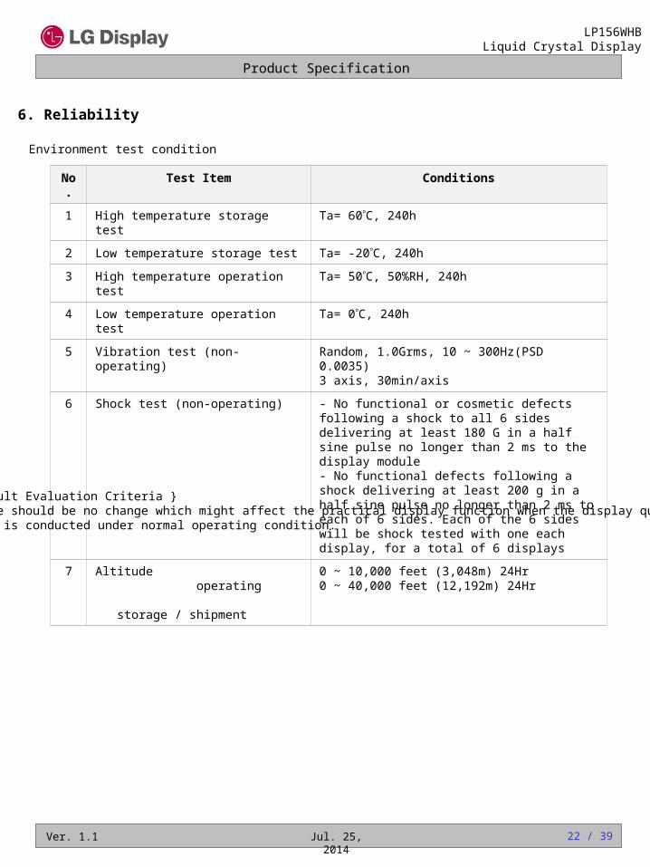
6. Reliability
Environment test condition
Result Evaluation Criteria There should be no change which might affect the practical display function when the display quality test is conducted under normal operating condition.
No.
Test Item Conditions
1 High temperature storage test Ta= 60C, 240h
2 Low temperature storage test Ta= -20C, 240h
3 High temperature operation test Ta= 50C, 50%RH, 240h
4 Low temperature operation test Ta= 0C, 240h
5 Vibration test (non-operating) Random, 1.0Grms, 10 ~ 300Hz(PSD 0.0035)3 axis, 30min/axis
6 Shock test (non-operating) - No functional or cosmetic defects following a shock to all 6 sides delivering at least 180 G in a half sine pulse no longer than 2 ms to the display module - No functional defects following a shock delivering at least 200 g in a half sine pulse no longer than 2 ms to each of 6 sides. Each of the 6 sides will be shock tested with one each display, for a total of 6 displays
7 Altitude operating storage / shipment
0 ~ 10,000 feet (3,048m) 24Hr0 ~ 40,000 feet (12,192m) 24Hr
Product Specification
LP156WHBLiquid Crystal Display
Ver. 1.1 Jul. 25, 2014
7. International Standards
7-1. Safety
7-2. Environment
a) RoHS, Directive 2011/65/EU of the European Parliament and of the council of 8 June 2011
a) UL 60950-1, Underwriters Laboratories Inc. Information Technology Equipment - Safety - Part 1 : General Requirements.b) CAN/CSA-C22.2 No. 60950-1-07, Canadian Standards Association. Information Technology Equipment - Safety - Part 1 : General Requirements.c) EN 60950-1, European Committee for Electro technical Standardization (CENELEC). Information Technology Equipment - Safety - Part 1 : General Requirements.d) IEC 60950-1, The International Electro technical Commission (IEC). Information Technology Equipment - Safety - Part 1 : General Requirements
23 / 39
Product Specification
LP156WHBLiquid Crystal Display
Ver. 1.1 Jul. 25, 2014
8. Packing
8-2. Packing Form
a) Package quantity in one box : 20pcs
b) Box Size : 478mm X 365mm X 328mm
8-1. Designation of Lot Marka) Lot Mark
A B C D E F G H I J K L M
A,B,C : SIZE(INCH) D : YEAR E : MONTH F ~ M : SERIAL NO.
Note 1. YEAR
2. MONTH
Mark
Year
K
2020
F
2016
G
2017
H
2018
J
2019
D
2014
E
2015
CBA
201320122011
B
Nov
Mark
Month
A
Oct
6
Jun
7
Jul
8
Aug
9
Sep
4
Apr
5
May
C321
DecMarFebJan
b) Location of Lot Mark
Serial No. is printed on the label. The label is attached to the backside of the LCD module.This is subject to change without prior notice.
24 / 40
3. Factory Code
N O P
N: PANEL FACTORY O : MODULE FACTORY P ~ Q: SERIAL NO.
(Not included in barcode)
Panel Factory P5 P6
Mark 5 6
Q
Module Factory NJ HS NJ ST
Mark P D
※ For your better understanding, please see the label on the drawing in page 21
Product Specification
LP156WHBLiquid Crystal Display
Ver. 1.1 Jul. 25, 2014 25 / 39
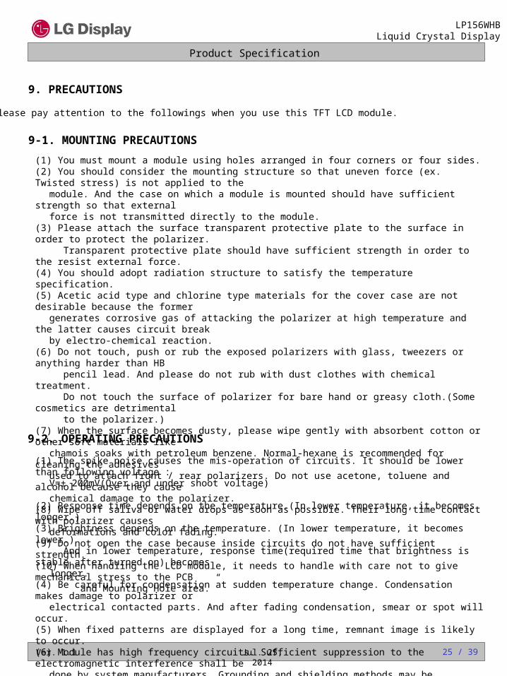
9. PRECAUTIONS
Please pay attention to the followings when you use this TFT LCD module.
9-1. MOUNTING PRECAUTIONS
(1) You must mount a module using holes arranged in four corners or four sides.(2) You should consider the mounting structure so that uneven force (ex. Twisted stress) is not applied to the module. And the case on which a module is mounted should have sufficient strength so that external
force is not transmitted directly to the module.(3) Please attach the surface transparent protective plate to the surface in order to protect the polarizer. Transparent protective plate should have sufficient strength in order to the resist external force.(4) You should adopt radiation structure to satisfy the temperature specification.(5) Acetic acid type and chlorine type materials for the cover case are not desirable because the former generates corrosive gas of attacking the polarizer at high temperature and the latter causes circuit break
by electro-chemical reaction.(6) Do not touch, push or rub the exposed polarizers with glass, tweezers or anything harder than HB pencil lead. And please do not rub with dust clothes with chemical treatment. Do not touch the surface of polarizer for bare hand or greasy cloth.(Some cosmetics are detrimental to the polarizer.)(7) When the surface becomes dusty, please wipe gently with absorbent cotton or other soft materials like
chamois soaks with petroleum benzene. Normal-hexane is recommended for cleaning the adhesives used to attach front / rear polarizers. Do not use acetone, toluene and alcohol because they cause chemical damage to the polarizer.
(8) Wipe off saliva or water drops as soon as possible. Their long time contact with polarizer causes deformations and color fading.
(9) Do not open the case because inside circuits do not have sufficient strength. (10) When handling the LCD module, it needs to handle with care not to give mechanical stress to the PCB and Mounting Hole area.”
9-2. OPERATING PRECAUTIONS
(1) The spike noise causes the mis-operation of circuits. It should be lower than following voltage : V=± 200mV(Over and under shoot voltage)
(2) Response time depends on the temperature.(In lower temperature, it becomes longer.)(3) Brightness depends on the temperature. (In lower temperature, it becomes lower.) And in lower temperature, response time(required time that brightness is stable after turned on) becomes longer.(4) Be careful for condensation at sudden temperature change. Condensation makes damage to polarizer or
electrical contacted parts. And after fading condensation, smear or spot will occur.(5) When fixed patterns are displayed for a long time, remnant image is likely to occur.(6) Module has high frequency circuits. Sufficient suppression to the electromagnetic interference shall be
done by system manufacturers. Grounding and shielding methods may be important to minimized the interference.
Product Specification
LP156WHBLiquid Crystal Display
Ver. 1.1 Jul. 25, 2014 26 / 39
Since a module is composed of electronic circuits, it is not strong to electrostatic discharge. Make certain that treatment persons are connected to ground through wrist band etc. And don’t touch interface pin directly.
9-3. ELECTROSTATIC DISCHARGE CONTROL
Strong light exposure causes degradation of polarizer and color filter.
9-4. PRECAUTIONS FOR STRONG LIGHT EXPOSURE
9-5. STORAGE
(1) When the protection film is peeled off, static electricity is generated between the film and polarizer. This should be peeled off slowly and carefully by people who are electrically grounded and with well ion-blown equipment or in such a condition, etc.(2) The protection film is attached to the polarizer with a small amount of glue. If some stress is applied to rub the protection film against the polarizer during the time you peel off the film, the glue is apt to remain on the polarizer. Please carefully peel off the protection film without rubbing it against the polarizer.(3) When the module with protection film attached is stored for a long time, sometimes there remains a very small amount of glue still on the polarizer after the protection film is peeled off.(4) You can remove the glue easily. When the glue remains on the polarizer surface or its vestige is recognized, please wipe them off with absorbent cotton waste or other soft material like chamois soaked with normal-hexane.
9-6. HANDLING PRECAUTIONS FOR PROTECTION FILM
When storing modules as spares for a long time, the following precautions are necessary.
(1) Store them in a dark place. Do not expose the module to sunlight or fluorescent light. Keep the temperature between 5C and 35C at normal humidity.
(2) The polarizer surface should not come in contact with any other object. It is recommended that they be stored in the container in which they were shipped.
9-7. THE LGD QA RESPONSIBILITY WILL BE AVOIDED IN CASE OF BELOW
(1) When the customer attaches TSM(Touch Sensor Module) on LCM without Supplier’s approval.(2) When the customer attaches cover glass on LCM without Supplier’s approval.(3) When the LCMs were repaired by 3rd party without Supplier’s approval.(4) When the LCMs were treated like Disassemble and Rework by the Customer and/or Customer’s representatives without supplier’s approval.
Product Specification
LP156WHBLiquid Crystal Display
Ver. 1.1 Jul. 25, 2014 27 / 39
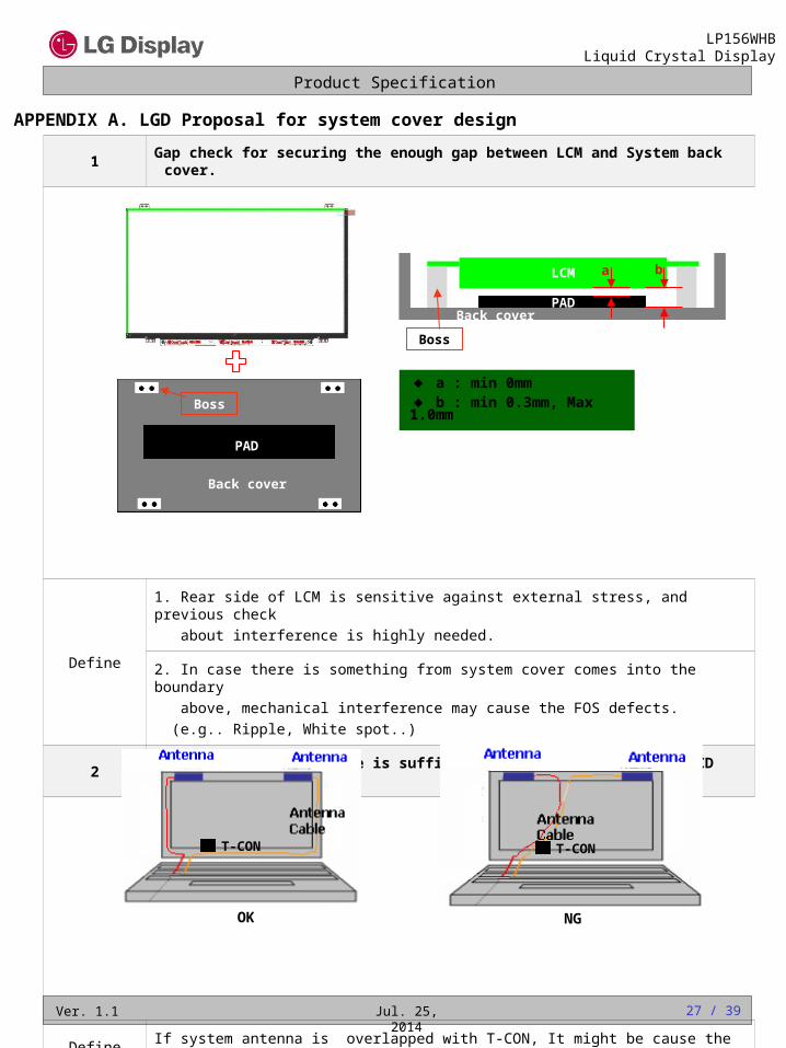
1 Gap check for securing the enough gap between LCM and System back cover.
Define
1. Rear side of LCM is sensitive against external stress, and previous check
about interference is highly needed.
2. In case there is something from system cover comes into the boundary
above, mechanical interference may cause the FOS defects.
(e.g.. Ripple, White spot..)
2 Check if antenna cable is sufficiently apart from T-CON of LCD Module.
Define If system antenna is overlapped with T-CON, It might be cause the noise
NGOK
T-CONT-CON
LCM
PADBack cover
Boss
Back cover
PAD
Boss
a b
a : min 0mm b : min 0.3mm, Max 1.0mm
APPENDIX A. LGD Proposal for system cover design
Product Specification
LP156WHBLiquid Crystal Display
Ver. 1.1 Jul. 25, 2014 28 / 39
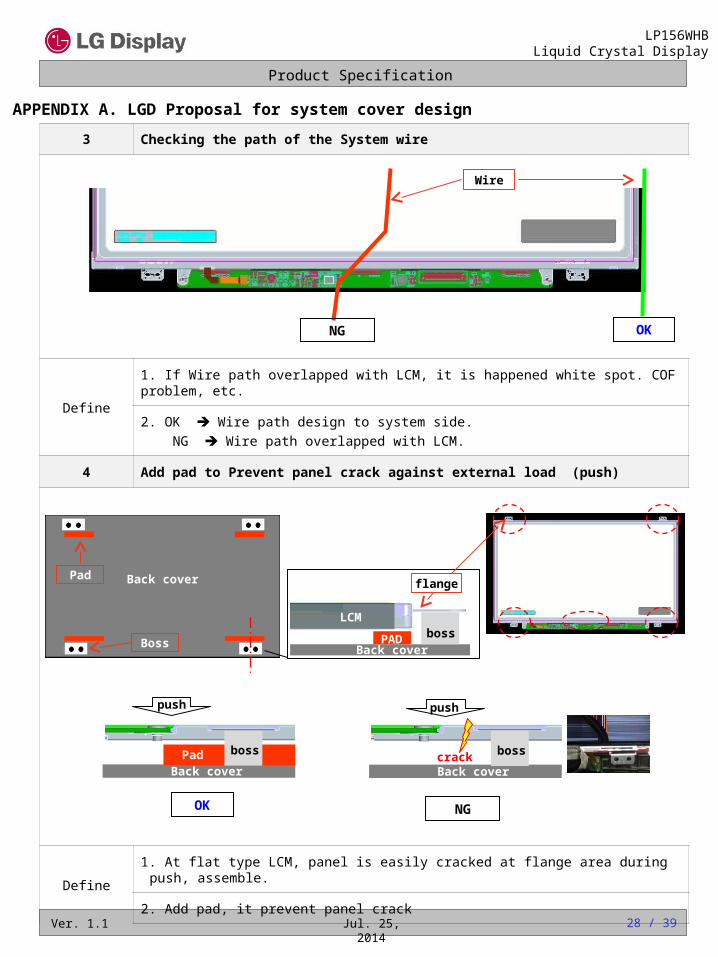
3 Checking the path of the System wire
Define
1. If Wire path overlapped with LCM, it is happened white spot. COF problem, etc.
2. OK Wire path design to system side.
NG Wire path overlapped with LCM.
4 Add pad to Prevent panel crack against external load (push)
Define1. At flat type LCM, panel is easily cracked at flange area during push, assemble.
2. Add pad, it prevent panel crack
OKNG
Wire
Back cover
Boss
Padflange
Back coverPAD
LCMboss
Back coverbossbossPad
push
Back coverbossboss
push
crack
OK NG
APPENDIX A. LGD Proposal for system cover design
Product Specification
LP156WHBLiquid Crystal Display
Ver. 1.1 Jul. 25, 2014 29 / 39
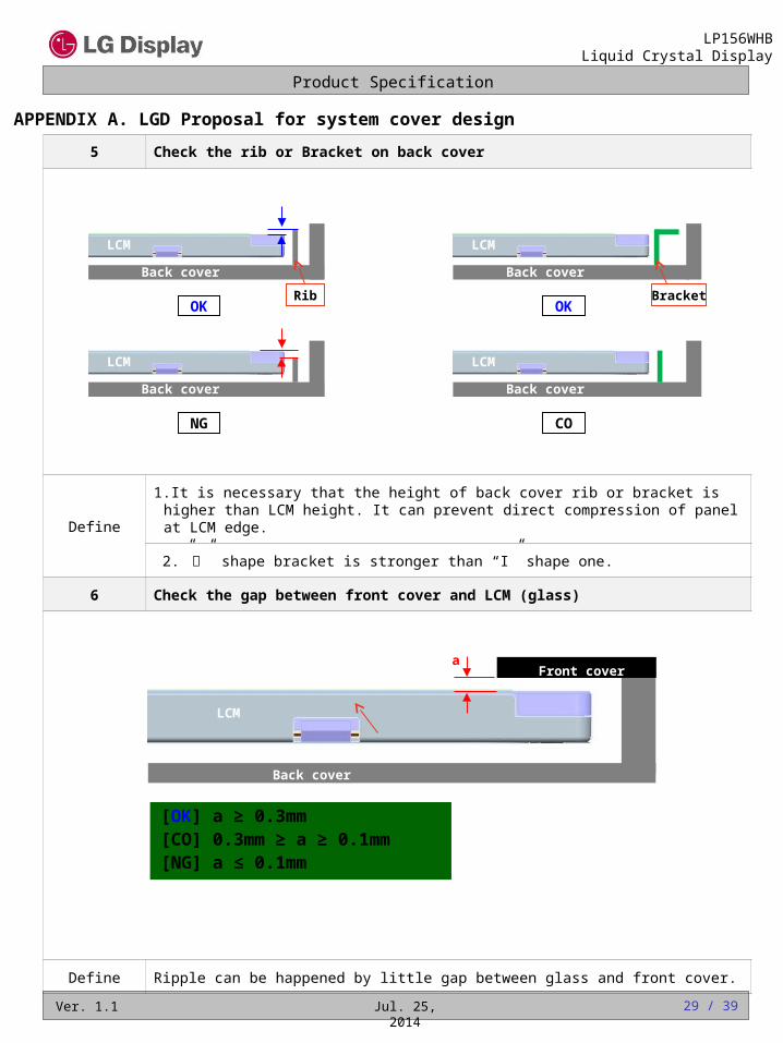
5 Check the rib or Bracket on back cover
Define
1.It is necessary that the height of back cover rib or bracket is higher than LCM height. It can prevent direct compression of panel at LCM edge.
2.” ㄱ” shape bracket is stronger than “I” shape one.
6 Check the gap between front cover and LCM (glass)
Define Ripple can be happened by little gap between glass and front cover.
Back cover
LCM
RibOK
Back cover
LCM
NG
Back cover
LCM
BracketOK
Back cover
LCM
CO
Back cover
LCM
Front covera
[OK] a ≥ 0.3mm[CO] 0.3mm ≥ a ≥ 0.1mm[NG] a ≤ 0.1mm
APPENDIX A. LGD Proposal for system cover design
Product Specification
LP156WHBLiquid Crystal Display
Ver. 1.1 Jul. 25, 2014 30 / 39
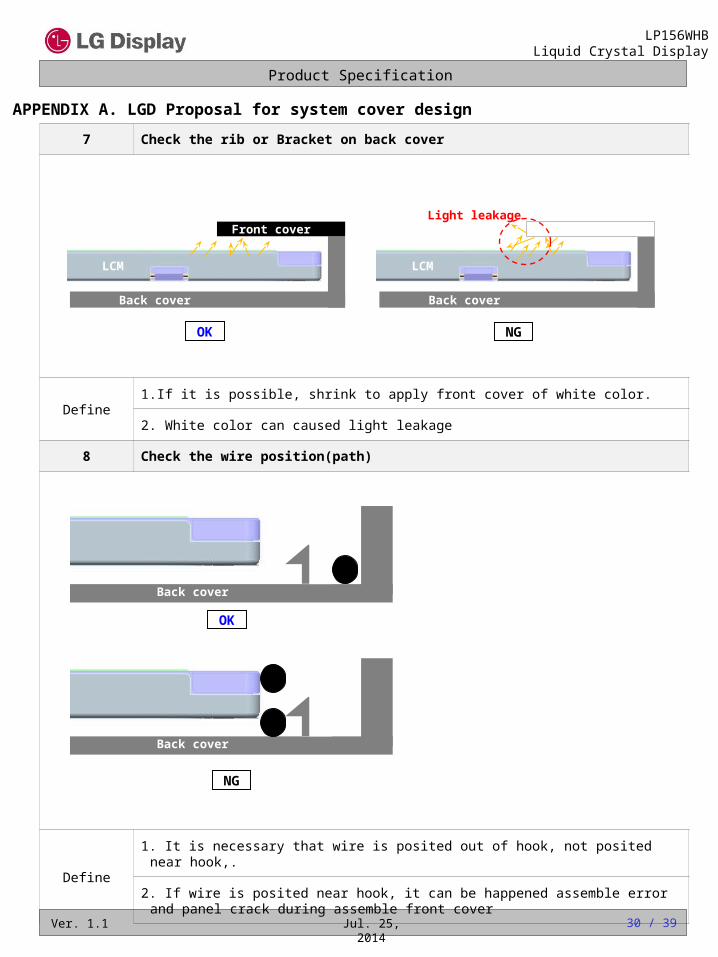
7 Check the rib or Bracket on back cover
Define1.If it is possible, shrink to apply front cover of white color.
2. White color can caused light leakage
8 Check the wire position(path)
Define
1. It is necessary that wire is posited out of hook, not posited near hook,.
2. If wire is posited near hook, it can be happened assemble error and panel crack during assemble front cover
Back cover
Back cover
LCM
Front cover
Back cover
LCM
Front coverLight leakage
Back cover
OK
NG
OK NG
APPENDIX A. LGD Proposal for system cover design
Product Specification
LP156WHBLiquid Crystal Display
Ver. 1.1 Jul. 25, 2014 31 / 39
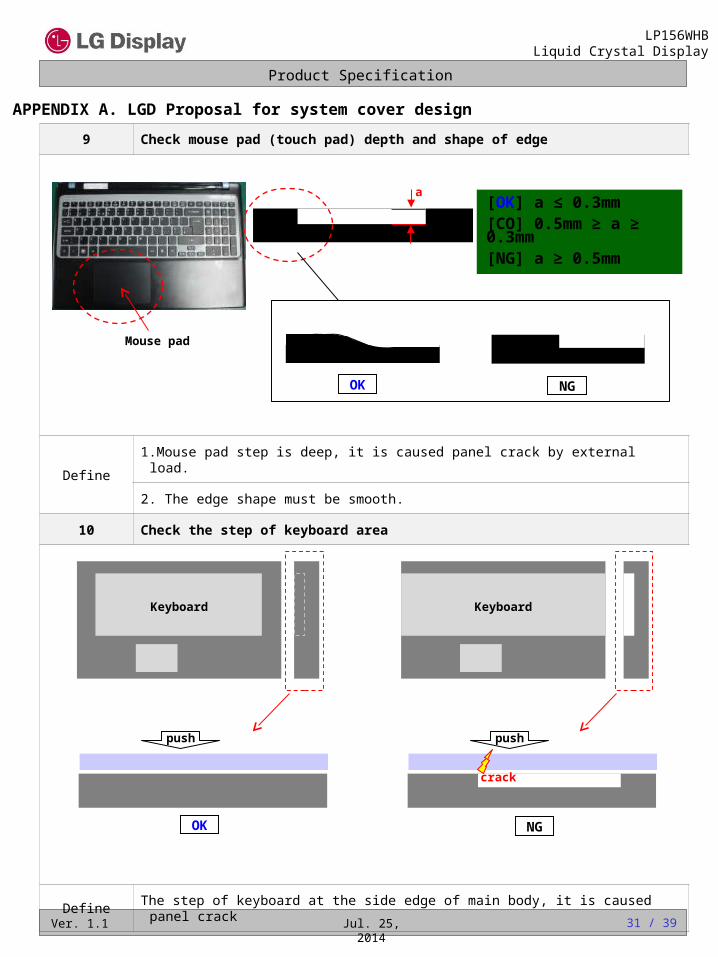
9 Check mouse pad (touch pad) depth and shape of edge
Define1.Mouse pad step is deep, it is caused panel crack by external load.
2. The edge shape must be smooth.
10 Check the step of keyboard area
Define The step of keyboard at the side edge of main body, it is caused panel crack
OK NG
Mouse pad
a[OK] a ≤ 0.3mm[CO] 0.5mm ≥ a ≥ 0.3mm[NG] a ≥ 0.5mm
Keyboard Keyboard
OK NG
push
crack
push
APPENDIX A. LGD Proposal for system cover design
Product Specification
LP156WHBLiquid Crystal Display
Ver. 1.1 Jul. 25, 2014 32 / 39
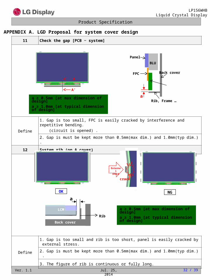
11 Check the gap [PCB ~ system]
Define
1. Gap is too small, FPC is easily cracked by interference and repetitive bending.
(circuit is opened) .
2. Gap is must be kept more than 0.5mm(max dim.) and 1.0mm(typ dim.) .
12 System rib (on A cover)
Define
1. Gap is too small and rib is too short, panel is easily cracked by external stress.
2. Gap is must be kept more than 0.5mm(max dim.) and 1.0mm(typ dim.) .
3. The figure of rib is continuous or fully long.
A
A’
a
Panel
BLU
Back cover
Rib, Frame …
FPC
a ≥ 0.5mm [at max dimension of design]a ≥ 1.0mm [at typical dimension of design]
OK NG
Back cover
LCM
Rib
a
Externalshock
crack
a ≥ 0.5mm [at max dimension of design]a ≥ 1.0mm [at typical dimension of design]
APPENDIX A. LGD Proposal for system cover design
Product Specification
LP156WHBLiquid Crystal Display
Ver. 1.1 Jul. 25, 2014
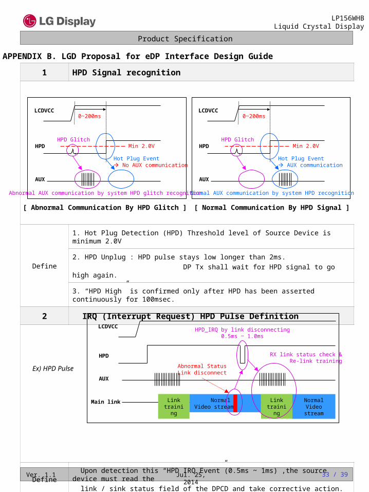
1 HPD Signal recognition
Define
1. Hot Plug Detection (HPD) Threshold level of Source Device is minimum 2.0V
2. HPD Unplug : HPD pulse stays low longer than 2ms.
DP Tx shall wait for HPD signal to go high again.
3. “HPD High” is confirmed only after HPD has been asserted continuously for 100msec.
2 IRQ (Interrupt Request) HPD Pulse Definition
Define Upon detection this “HPD IRQ Event”(0.5ms ~ 1ms) ,the source device must read the
link / sink status field of the DPCD and take corrective action.
APPENDIX B. LGD Proposal for eDP Interface Design Guide
[ Abnormal Communication By HPD Glitch ]
LCDVCC
HPD
AUX
0~200ms
Abnormal AUX communication by system HPD glitch recognition
HPD Glitch
Hot Plug Event No AUX communication
[ Normal Communication By HPD Signal ]
LCDVCC
HPD
AUX
0~200ms
Normal AUX communication by system HPD recognition
HPD Glitch
Hot Plug Event AUX communication
Min 2.0VMin 2.0V
LCDVCC
HPD
AUX
Main link Link training
NormalVideo stream
Abnormal StatusLink disconnect
HPD_IRQ by link disconnecting0.5ms ~ 1.0ms
Link training
NormalVideo stream
RX link status check &Re-link training
Ex) HPD Pulse
33 / 39
Product Specification
LP156WHBLiquid Crystal Display
Ver. 1.1 Jul. 25, 2014
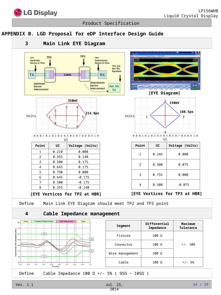
3 Main Link EYE Diagram
Define Main Link EYE Diagram should meet TP2 and TP3 point
4 Cable Impedance management
Define Cable Impedance 100 Ω +/- 5% ( 95Ω ~ 105Ω )
Point UI Voltage (Volts)
1 0.246 0.000
2 0.500 0.075
3 0.755 0.000
4 0.500 -0.075
[EYE Vertices for TP3 at HBR]
Point UI Voltage (Volts)
1 0.210 0.000
2 0.355 0.140
3 0.500 0.175
4 0.645 0.175
5 0.790 0.000
6 0.645 -0.175
7 0.500 -0.175
8 0.355 -0.140
[EYE Vertices for TP2 at HBR]
[EYE Diagram]
SegmentDifferentialImpedance
MaximumTolerance
Fixture 100 Ω
+/- 10%Connector 100 Ω
Wire management 100 Ω
Cable 100 Ω +/- 5%
214.8ps
350mV
UI
Volts
0.0 0.1 0.2 0.3 0.4 0.5 0.6 0.7 0.8 0.9 1.0
1
23 4
5
678
150mV
188.5psVolts 1
2
3
4
UI0.0 0.1 0.2 0.3 0.4 0.5 0.6 0.7 0.8 0.9 1.0
34 / 39
APPENDIX B. LGD Proposal for eDP Interface Design Guide
Product Specification
LP156WHBLiquid Crystal Display
Ver. 1.1 Jul. 25, 2014
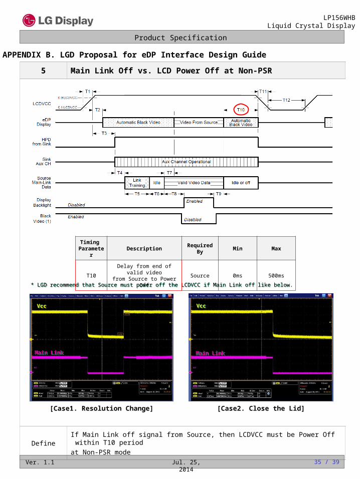
5 Main Link Off vs. LCD Power Off at Non-PSR
DefineIf Main Link off signal from Source, then LCDVCC must be Power Off within T10 period
at Non-PSR mode
* LGD recommend that Source must power off the LCDVCC if Main Link off like below. * LGD recommend that Source must power off the LCDVCC if Main Link off like below.
VccVcc
Main LinkMain Link
VccVcc
Main LinkMain Link
[Case1. Resolution Change] [Case2. Close the Lid]
Timing Parameter
Description Required By Min Max
T10Delay from end of valid video
from Source to Power OffSource 0ms 500ms
35 / 39
APPENDIX B. LGD Proposal for eDP Interface Design Guide
Product Specification
LP156WHBLiquid Crystal Display
Ver. 1.1 Jul. 25, 2014
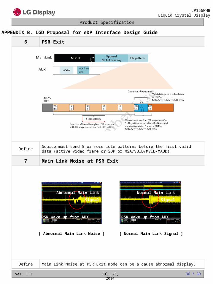
6 PSR Exit
DefineSource must send 5 or more idle patterns before the first valid data (active video frame or SDP or MSA/VBID/MVID/MAUD)
7 Main Link Noise at PSR Exit
Define Main Link Noise at PSR Exit mode can be a cause abnormal display.
Abnormal Main Link
Signal
Normal Main Link
Signal
PSR Wake up from AUX PSR Wake up from AUX
[ Abnormal Main Link Noise ] [ Normal Main Link Signal ]
36 / 39
APPENDIX B. LGD Proposal for eDP Interface Design Guide
Product Specification
LP156WHBLiquid Crystal Display
Ver. 1.1 Jul. 25, 2014 37 / 39
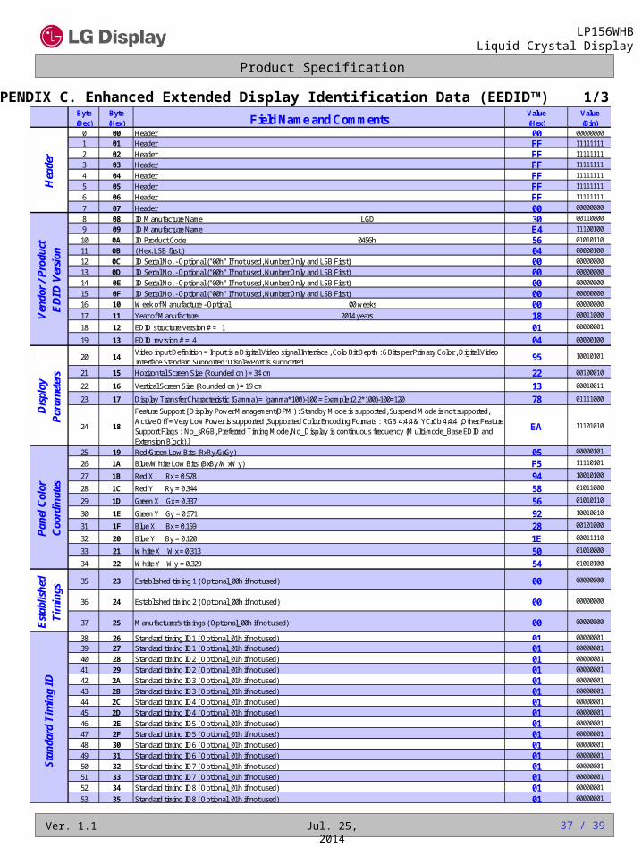
APPENDIX C. Enhanced Extended Display Identification Data (EEDIDTM) 1/3Byte(Dec)
Byte(Hex) Field Name and Comments
Value(Hex)
Value(Bin)
0 00 Header 00 00000000
1 01 Header FF 11111111
2 02 Header FF 11111111
3 03 Header FF 11111111
4 04 Header FF 11111111
5 05 Header FF 11111111
6 06 Header FF 11111111
7 07 Header 00 00000000
8 08 ID Manufacture Name LGD 30 00110000
9 09 ID Manufacture Name E4 11100100
10 0A ID Product Code 0456h 56 01010110
11 0B ( Hex. LSB first ) 04 00000100
12 0C ID Serial No. - Optional ("00h" If not used, Number Only and LSB First) 00 00000000
13 0D ID Serial No. - Optional ("00h" If not used, Number Only and LSB First) 00 00000000
14 0E ID Serial No. - Optional ("00h" If not used, Number Only and LSB First) 00 00000000
15 0F ID Serial No. - Optional ("00h" If not used, Number Only and LSB First) 00 00000000
16 10 Week of Manufacture - Optinal 00 weeks 00 00000000
17 11 Year of Manufacture 2014 years 18 00011000
18 12 EDID structure version # = 1 01 00000001
19 13 EDID revision # = 4 04 00000100
20 14Video input Definition = Input is a Digital Video signal Interface , Colo Bit Depth : 6 Bits per Primary Color , Digital VideoInterface Standard Supported: DisplayPort is supported
95 10010101
21 15 Horizontal Screen Size (Rounded cm) = 34 cm 22 00100010
22 16 Vertical Screen Size (Rounded cm) = 19 cm 13 00010011
23 17 Display Transfer Characteristic (Gamma) = (gamma*100)-100 = Example:(2.2*100)-100=120 78 01111000
24 18
Feature Support [ Display Power Management(DPM) : Standby Mode is supported, Suspend Mode is not supported,Active Off = Very Low Power is supported ,Supportted Color Encoding Formats : RGB 4:4:4 & YCrCb 4:4:4 ,Other FeatureSupport Flags : No_sRGB, Preferred Timing Mode, No_Display is continuous frequency (Multi-mode_Base EDID andExtension Block).]
EA 11101010
25 19 Red/Green Low Bits (RxRy/GxGy) 05 00000101
26 1A Blue/White Low Bits (BxBy/WxWy) F5 11110101
27 1B Red X Rx = 0.578 94 10010100
28 1C Red Y Ry = 0.344 58 01011000
29 1D Green X Gx = 0.337 56 01010110
30 1E Green Y Gy = 0.571 92 10010010
31 1F Blue X Bx = 0.159 28 00101000
32 20 Blue Y By = 0.120 1E 00011110
33 21 White X Wx = 0.313 50 01010000
34 22 White Y Wy = 0.329 54 01010100
35 23 Established timing 1 ( Optional_00h if not used) 00 00000000
36 24 Established timing 2 ( Optional_00h if not used) 00 00000000
37 25 Manufacturer's timings ( Optional_00h if not used) 00 00000000
38 26 Standard timing ID1 ( Optional_01h if not used) 01 00000001
39 27 Standard timing ID1 ( Optional_01h if not used) 01 00000001
40 28 Standard timing ID2 ( Optional_01h if not used) 01 00000001
41 29 Standard timing ID2 ( Optional_01h if not used) 01 00000001
42 2A Standard timing ID3 ( Optional_01h if not used) 01 00000001
43 2B Standard timing ID3 ( Optional_01h if not used) 01 00000001
44 2C Standard timing ID4 ( Optional_01h if not used) 01 00000001
45 2D Standard timing ID4 ( Optional_01h if not used) 01 00000001
46 2E Standard timing ID5 ( Optional_01h if not used) 01 00000001
47 2F Standard timing ID5 ( Optional_01h if not used) 01 00000001
48 30 Standard timing ID6 ( Optional_01h if not used) 01 00000001
49 31 Standard timing ID6 ( Optional_01h if not used) 01 00000001
50 32 Standard timing ID7 ( Optional_01h if not used) 01 00000001
51 33 Standard timing ID7 ( Optional_01h if not used) 01 00000001
52 34 Standard timing ID8 ( Optional_01h if not used) 01 00000001
53 35 Standard timing ID8 ( Optional_01h if not used) 01 00000001
Est
ablis
hed
Tim
ings
Sta
nda
rd T
imin
g ID
Dis
play
Par
amet
ers
Pan
el C
olor
Coo
rdin
ates
Hea
der
Ven
dor
/ Pro
duct
ED
ID V
ersi
on
Product Specification
LP156WHBLiquid Crystal Display
Ver. 1.1 Jul. 25, 2014 38 / 39
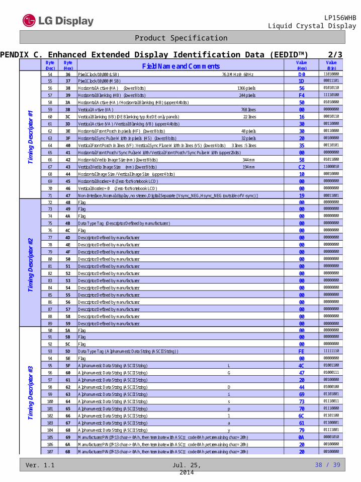
APPENDIX C. Enhanced Extended Display Identification Data (EEDIDTM) 2/3Byte(Dec)
Byte(Hex) Field Name and Comments
Value(Hex)
Value(Bin)
54 36 Pixel Clock/10,000 (LSB) 76.3 MHz @ 60 Hz D0 11010000
55 37 Pixel Clock/10,000 (MSB) 1D 00011101
56 38 Horizontal Active (HA) (lower 8 bits) 1366 pixels 56 01010110
57 39 Horizontal Blanking (HB) (lower 8 bits) 244 pixels F4 11110100
58 3A Horizontal Active (HA) / Horizontal Blanking (HB) (upper 4:4bits) 50 01010000
59 3B Vertical Avtive (VA) 768 lines 00 00000000
60 3C Vertical Blanking (VB) (DE Blanking typ.for DE only panels) 22 lines 16 00010110
61 3D Vertical Active (VA) / Vertical Blanking (VB) (upper 4:4bits) 30 00110000
62 3E Horizontal Front Porch in pixels (HF) (lower 8 bits) 48 pixels 30 00110000
63 3F Horizontal Sync Pulse Width in pixels (HS) (lower 8 bits) 32 pixels 20 00100000
64 40 Vertical Front Porch in lines (VF) : Vertical Sync Pluse Width in lines (VS) (lower 4 bits) 3 lines : 5 lines 35 00110101
65 41 Horizontal Front Porch/ Sync Pulse Width/ Vertical Front Porch/ Sync Pulse Width (upper 2bits) 00 00000000
66 42 Horizontal Vedio Image Size (mm) (lower 8 bits) 344 mm 58 01011000
67 43 Vertical Vedio Image Size (mm) (lower 8 bits) 194 mm C2 11000010
68 44 Horizontal Image Size / Vertical Image Size (upper 4 bits) 10 00010000
69 45 Horizontal Border = 0 (Zero for Notebook LCD) 00 00000000
70 46 Vertical Border = 0 (Zero for Notebook LCD) 00 00000000
71 47 Non-Interlace, Normal display, no stereo, Digital Separate [ Vsync_NEG, Hsync_NEG (outside of V-sync) ] 19 00011001
72 48 Flag 00 00000000
73 49 Flag 00 00000000
74 4A Flag 00 00000000
75 4B Data Type Tag (Descriptor Defined by manufacturer ) 00 00000000
76 4C Flag 00 00000000
77 4D Descriptor Defined by manufacturer 00 00000000
78 4E Descriptor Defined by manufacturer 00 00000000
79 4F Descriptor Defined by manufacturer 00 00000000
80 50 Descriptor Defined by manufacturer 00 00000000
81 51 Descriptor Defined by manufacturer 00 00000000
82 52 Descriptor Defined by manufacturer 00 00000000
83 53 Descriptor Defined by manufacturer 00 00000000
84 54 Descriptor Defined by manufacturer 00 00000000
85 55 Descriptor Defined by manufacturer 00 00000000
86 56 Descriptor Defined by manufacturer 00 00000000
87 57 Descriptor Defined by manufacturer 00 00000000
88 58 Descriptor Defined by manufacturer 00 00000000
89 59 Descriptor Defined by manufacturer 00 00000000
90 5A Flag 00 00000000
91 5B Flag 00 00000000
92 5C Flag 00 00000000
93 5D Data Type Tag ( Alphanumeric Data String (ASCII String) ) FE 11111110
94 5E Flag 00 00000000
95 5F Alphanumeric Data String (ASCII String) L 4C 01001100
96 60 Alphanumeric Data String (ASCII String) G 47 01000111
97 61 Alphanumeric Data String (ASCII String) 20 00100000
98 62 Alphanumeric Data String (ASCII String) D 44 01000100
99 63 Alphanumeric Data String (ASCII String) i 69 01101001
100 64 Alphanumeric Data String (ASCII String) s 73 01110011
101 65 Alphanumeric Data String (ASCII String) p 70 01110000
102 66 Alphanumeric Data String (ASCII String) l 6C 01101100
103 67 Alphanumeric Data String (ASCII String) a 61 01100001
104 68 Alphanumeric Data String (ASCII String) y 79 01111001
105 69 Manufacturer P/N(If<13 char--> 0Ah, then terminate with ASCⅡ code 0Ah,set remaining char = 20h) 0A 00001010
106 6A Manufacturer P/N(If<13 char--> 0Ah, then terminate with ASCⅡ code 0Ah,set remaining char = 20h) 20 00100000
107 6B Manufacturer P/N(If<13 char--> 0Ah, then terminate with ASCⅡ code 0Ah,set remaining char = 20h) 20 00100000
Tim
ing
Des
crip
tor
#3T
imin
g D
escr
ipto
r #1
Tim
ing
Des
crip
tor
#2
Product Specification
LP156WHBLiquid Crystal Display
Ver. 1.1 Jul. 25, 2014 39 / 39
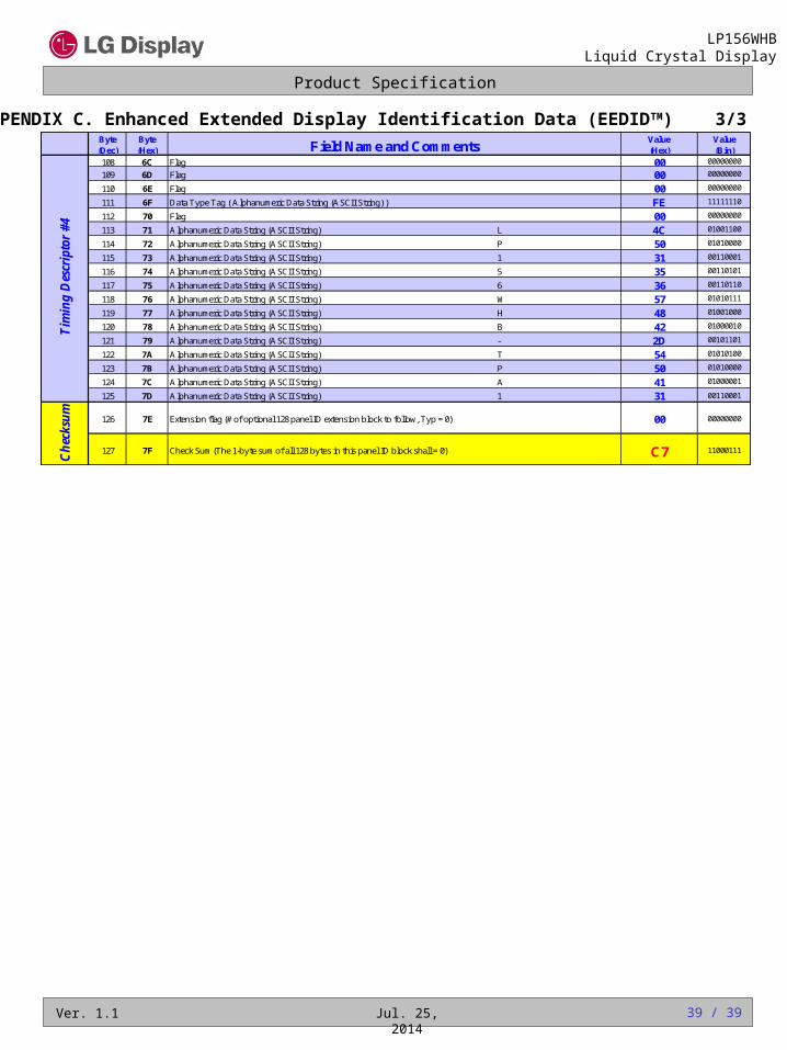
APPENDIX C. Enhanced Extended Display Identification Data (EEDIDTM) 3/3Byte(Dec)
Byte(Hex) Field Name and Comments
Value(Hex)
Value(Bin)
108 6C Flag 00 00000000
109 6D Flag 00 00000000
110 6E Flag 00 00000000
111 6F Data Type Tag ( Alphanumeric Data String (ASCII String) ) FE 11111110
112 70 Flag 00 00000000
113 71 Alphanumeric Data String (ASCII String) L 4C 01001100
114 72 Alphanumeric Data String (ASCII String) P 50 01010000
115 73 Alphanumeric Data String (ASCII String) 1 31 00110001
116 74 Alphanumeric Data String (ASCII String) 5 35 00110101
117 75 Alphanumeric Data String (ASCII String) 6 36 00110110
118 76 Alphanumeric Data String (ASCII String) W 57 01010111
119 77 Alphanumeric Data String (ASCII String) H 48 01001000
120 78 Alphanumeric Data String (ASCII String) B 42 01000010
121 79 Alphanumeric Data String (ASCII String) - 2D 00101101
122 7A Alphanumeric Data String (ASCII String) T 54 01010100
123 7B Alphanumeric Data String (ASCII String) P 50 01010000
124 7C Alphanumeric Data String (ASCII String) A 41 01000001
125 7D Alphanumeric Data String (ASCII String) 1 31 00110001
126 7E Extension flag (# of optional 128 panel ID extension block to follow, Typ = 0) 00 00000000
127 7F Check Sum (The 1-byte sum of all 128 bytes in this panel ID block shall = 0) C7 11000111
Tim
ing
Des
crip
tor
#4
Ch
ecks
um