Embed Size (px)
Citation preview

PRODUCT SPECIFICATION File: 400Slim-1U-A06 Date: Nov 20, 2019
SWITCHING POWER SUPPLY Page:1 of 22
Model: S1M-401SGP2 (PMBus) Rev.:A0.6
1 GENERAL SCOPE
This specification defines the performance characteristics of a grounded, AC input, 400 watts, 2 outputs power supply. This specification also defines worldwide safety requirements and manufactures process test requirements.
2 Power Input Specification 2.1 Input Voltage The power supply must operate within all specified limits over the following input voltage range. The power supply shall operate properly at 85 VAC input voltage to guarantee proper design margins.
PARAMETER MIN RATED MAX PEAK
Voltage (110) 90 Vrms 100 – 127 Vrms 140 Vrms
Current 6A Max.
Voltage (220) 180 Vrms 200 – 240 Vrms 264 Vrms
Current 3A Max.
Frequency 47 Hz 50 – 60 Hz 63 Hz
2.2 AC Inrush Current
AC line inrush current shall not exceed 30A peak, for up to one‐quarter of the AC cycle, after which, the input current should be no more than the specified maximum input current. The peak inrush current shall be less than the ratings of its critical components (including input fuse, bulk rectifiers, and surge limiting device).
The power supply must meet the inrush requirements for any rated AC voltage, during turn on at any phase of AC voltage, during a single cycle AC dropout condition as well as upon recovery after AC dropout of any duration, and over the specified temperature range (Top).
2.3 Efficiency, Power Factor Correction and iTHD
Load(%) 115Vac 60Hz 230Vac 50Hz
Max. iTHD (%)
Min. PowerFactor
Min. Efficiency(%)
Max. iTHD (%)
Min. Power Factor
Min. Efficiency(%)
20% 10 0.95 10 0.95 90 50% 8 0.95 8 0.95 94 100% 5 0.95 5 0.95 91
PRODUCT SPECIFICATION File: 400Slim-1U-A06 Date: Nov 20, 2019
SWITCHING POWER SUPPLY Page:2 of 22
Model: S1M-401SGP2 (PMBus) Rev.:A0.6
2.4 AC Line Dropout / Holdup
An AC line dropout is defined to be when the AC input drops to 0VAC at any phase of the AC line for any length of time. During an AC dropout the power supply must meet dynamic voltage regulation requirements. An AC line dropout of any duration shall not cause tripping of control signals or protection circuits. If the AC dropout lasts longer than the holdup time the power supply should recover and meet all turn on requirements. The power supply shall meet the AC dropout requirement over rated AC voltages and frequencies. A dropout of the AC line for any duration shall not cause damage to the power supply.
Loading Holdup Time
100% 12ms
2.5 Susceptibility Requirements
The power supply shall meet the following electrical immunity requirements when connected to a cage with an external EMI filter, which meets the criteria defined in the SSI document EPS Power Supply Specification.
Level Description A The apparatus shall continue to operate as intended. No degradation of performance. B The apparatus shall continue to operate as intended. No degradation of performance beyond
spec. limits. C Temporary loss of function is allowed provided the function is self‐recoverable or can be
restored by the operation of the controls.
2.5.1 Electrical Discharge Susceptibility
The power supply shall comply with the limits defined in EN 55024:1998 using the IEC 61000‐4‐2:1995 test standard and performance criteria B defined in Annex B of CISPR 24.
2.5.2 Fast Transient/Burst
The power supply shall comply with the limits defined in EN55024:1998 using the IEC 61000‐4‐4:1995 test standard and performance criteria B define in Annex B of CISPR 24.
2.5.3 Radiated Immunity
The power supply shall comply with the limits defined in EN55024:1998 using the IEC61000‐4‐3:1995 test standard and performance criteria A defined in Annex B of CISPR 24.
2.5.4 Surge Immunity
The power supply shall be tested with the system for immunity to AC Ring wave and AC
PRODUCT SPECIFICATION File: 400Slim-1U-A06 Date: Nov 20, 2019
SWITCHING POWER SUPPLY Page:3 of 22
Model: S1M-401SGP2 (PMBus) Rev.:A0.6
Unidirectional wave, both up to 2kV(Differential mode 2K,Common mode 1K), per EN55024:1998, EN 61000‐4‐5:1995 and ANSI C62.45:1992.
The pass criteria include: No unsafe operation is allowed under any condition; all power supply output voltage levels to stay within proper spec levels; No change in operating state or loss of data during and after the test profile; No component damage under any condition.
The power supply shall comply with the limits defined in EN55024:1998 using the IEC 61000‐4‐5:1995 test standard and performance criteria B defined in Annex B f CISPR 24.
2.5.5 AC Line Transient Specification
AC line transient conditions shall be defined as “sag” and “surge” conditions. “Sag” conditions are also commonly referred to as “brownout”, these conditions will be defined as the AC line voltage dropping below nominal voltage conditions. “Surge” will be defined to refer to conditions when the AC line voltage rises above nominal voltage.
The power supply shall meet the requirements under the following AC line sag and surge conditions.
AC Line Sag Transient Performance (10sec interval between each sagging):
Duration Sag Operating AC Voltage Line Frequency Performance Criteria
0 to 1/2 AC cycle 95% Nominal AC Voltage ranges 50/60Hz No loss of function or performance
>1 AC cycle >30% Nominal AC Voltage ranges 50/60Hz Loss of function acceptable, self recoverable
AC Line Surge Transient Performance
Duration Surge Operating AC Voltage Line Performance Criteria
Continuous 10% Nominal AC Voltage ranges 50/60Hz No loss of function or performance
0 to 1/2 AC cycle 30% Mid‐point of nominal AC Voltages 50/60Hz No loss of function or performance
2.5.6 AC Line Fast Transient (EFT) Specification
The power supply shall meet the EN61000‐4‐5 directive and any additional requirements in IEC1000‐4‐5:1995 and the level 3 requirements for surge‐withstand capability, with the following conditions and exceptions:
z These input transients must not cause any out‐of‐regulation conditions, such as overshoot and undershoot, nor must it cause any nuisance trips of any of the power supply protection circuits.
z The surge‐withstand test must not produce damage to the power supply.
PRODUCT SPECIFICATION File: 400Slim-1U-A06 Date: Nov 20, 2019
SWITCHING POWER SUPPLY Page:4 of 22
Model: S1M-401SGP2 (PMBus) Rev.:A0.6
z The supply must meet surge‐withstand test conditions under maximum and minimum DC‐output load conditions.
2.5.7 Power Recovery
The power supply shall recover automatically (auto recover) after an AC power failure. AC power failure is defined to be any loss of AC power that exceeds the dropout criteria.
2.5.8 Voltage Brownout
Input voltage range for AC minimum startup voltage, 81 to 89VAC, and maximum turn off voltage range 71 to 79VAC
2.5.9 AC Line Leakage Current
The maximum leakage current to ground of power supply shall be 0.875mA when tested at 264Vac/60Hz.
3 Power Output Specification 3.1Grounding
The output ground of the pins of the power supply provides the output power return path. The ground output at the PCB card edge shall be connected to the safety ground (power supply enclosure). This grounding should be well designed to ensure passing the max allowed Common Mode Noise levels.
The power supply shall be provided with a reliable protective earth ground. All secondary circuits shall be connected to protective earth ground. Resistance of the ground returns to chassis shall not exceed 100 mΩ (Test Conditions 40A for 120sec). This path may be used to carry DC‐current
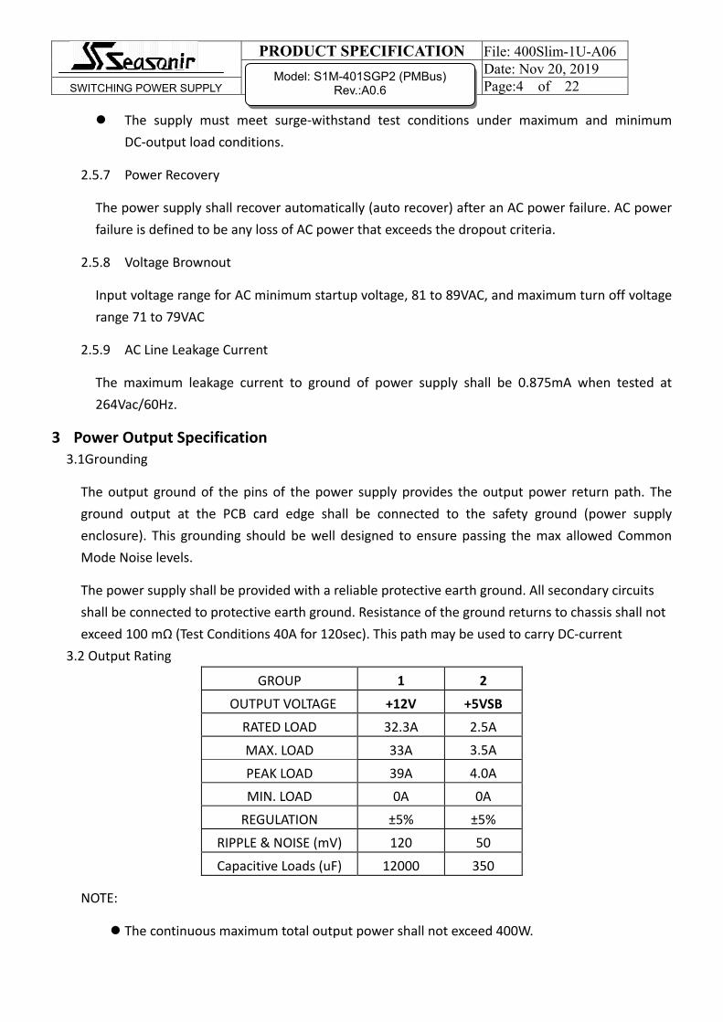
3.2 Output Rating
GROUP 1 2
OUTPUT VOLTAGE +12V +5VSB
RATED LOAD 32.3A 2.5A
MAX. LOAD 33A 3.5A
PEAK LOAD 39A 4.0A
MIN. LOAD 0A 0A
REGULATION ±5% ±5%
RIPPLE & NOISE (mV) 120 50
Capacitive Loads (uF) 12000 350
NOTE:
z The continuous maximum total output power shall not exceed 400W.
PRODUCT SPECIFICATION File: 400Slim-1U-A06 Date: Nov 20, 2019
SWITCHING POWER SUPPLY Page:5 of 22
Model: S1M-401SGP2 (PMBus) Rev.:A0.6
z Peak power and current loading should be supported for a minimum of 100ms.
z The power supply shall meet the voltage regulation under all operating conditions ( AC line, transient loading, output loading ). These limits include the peak‐peak ripple/noise.
z Ripple and Noise measuring with an oscilloscope with 20 MHz bandwidth. Output should be bypassed at the connector with a 0.1uF ceramic disk capacitor and a 10uF electrolytic capacitor to simulate system load. The length of ground wire on probe should not longer than 40mm, if a Non ‐ differential type of scope was used.
3.3 No Load Operation
The power supply shall meet all requirements except for the transient loading requirements when operated at no load on all outputs.
3.4 Dynamic Loading
The output voltages will remain within limits specified in 3.2 Output Voltage Regulation for the step loading and capacitive loading specified in the table below. The load transient repetition rate shall be tested between 50Hz and 5kHz at duty cycles ranging from 10%‐90%. The load transient repetition rate is only a test specification. The Δ step load may occur anywhere within the MIN load to the MAX load conditions.
Output Δ Step Load Size Load Slew Rate Test capacitive Load +12V 60% of max load 0.5A/μs 2000uF +5VSB 1.0A 0.5A/μs 20uF
Note: For dynamic condition +12V min loading is 1A.
3.5 Maximum Load Change
The power supply shall continue to operate normally when there is a step change d 1A/μsec, between minimum load and maximum load.
3.6 Close loop Stability
The power supply shall be unconditionally stable under all line/load/transient load conditions including capacitive load ranges. A minimum of: 45 degrees phase margin and ‐10dB gain margin is required.
Closed‐loop stability must be ensured at the maximum and minimum loads as applicable.
3.7 Residual Voltage Immunity in Standby mode
The power supply should be immune to any residual voltage placed on its outputs (Typically a leakage voltage through the system from standby output) up to 500mV. There shall be no additional

PRODUCT SPECIFICATION File: 400Slim-1U-A06 Date: Nov 20, 2019
SWITCHING POWER SUPPLY Page:6 of 22
Model: S1M-401SGP2 (PMBus) Rev.:A0.6
heat generated, nor stressing of any internal components with this voltage applied to any individual or all outputs simultaneously. It also should not trip the protection circuits during turn on.
The residual voltage at the power supply outputs for no load condition shall not exceed 100mV when AC voltage is applied and the PSON# signal is de‐asserted.
3.8 Soft Starting
The Power Supply shall contain control circuit which provides monotonic soft start for its outputs without overstress of the AC line or any power supply components at any specified AC line or load conditions.
3.9 Forced Load Sharing
The +12V output will have active load sharing. The output will share within 10% at full load. The failure of a power supply should not affect the load sharing or output voltages of the other supplies still operating. The supplies must be able to load share in parallel and operate in a hot‐swap / redundant 1+1 configurations.
Ishare Voltage % of max. current capacity Voltage level (+/‐ 10%) 50% 4V 100% 8V
3.10 Over shoot at Turn‐on/Turn‐off
Any output overshoot at turn on shall be less than 10% of the nominal output value. Any overshoot shall recover to be within regulation requirements in less than 10ms.
3.11 Undershoot at Turn‐on/Turn‐off
Any output shall not undershoot at turn on or off cycle under any circumstances.
4 Timing
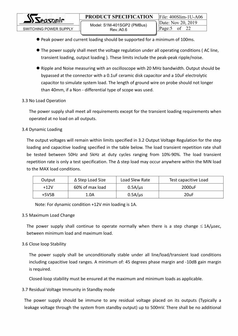
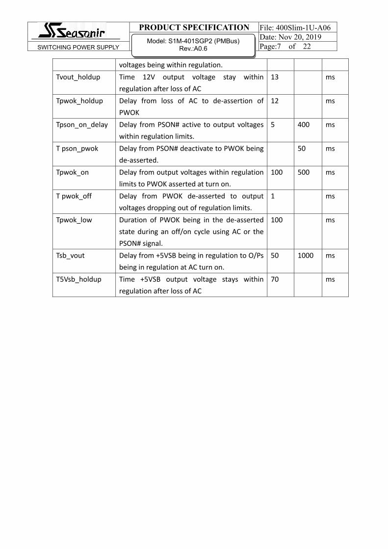
The output voltages rise from 10% to within regulation limits (Tvout_rise) within 5 to 70ms. For +5VSB, it rises from 1 to 25ms. All outputs rise monotonically. Table below shows the timing for the power supply being turned on and off via the AC input, with PSON held low and the PSON signal, with the AC input applied.
Item Description MIN MAX Units Tvout_rise Output voltage rise time 5.0 70 ms Tsb_on_delay Delay from AC being applied to +5VSB being
within regulation. 1500 ms
T ac_on_delay Delay from AC being applied to all output 3000 ms
PRODUCT SPECIFICATION File: 400Slim-1U-A06 Date: Nov 20, 2019
SWITCHING POWER SUPPLY Page:7 of 22
Model: S1M-401SGP2 (PMBus) Rev.:A0.6
voltages being within regulation. Tvout_holdup Time 12V output voltage stay within
regulation after loss of AC 13 ms
Tpwok_holdup Delay from loss of AC to de‐assertion of PWOK
12 ms
Tpson_on_delay Delay from PSON# active to output voltages within regulation limits.
5 400 ms
T pson_pwok Delay from PSON# deactivate to PWOK being de‐asserted.
50 ms
Tpwok_on Delay from output voltages within regulation limits to PWOK asserted at turn on.
100 500 ms
T pwok_off Delay from PWOK de‐asserted to output voltages dropping out of regulation limits.
1 ms
Tpwok_low Duration of PWOK being in the de‐asserted state during an off/on cycle using AC or the PSON# signal.
100 ms
Tsb_vout Delay from +5VSB being in regulation to O/Ps being in regulation at AC turn on.
50 1000 ms
T5Vsb_holdup Time +5VSB output voltage stays within regulation after loss of AC
70 ms
PRODUCT SPECIFICATION File: 400Slim-1U-A06 Date: Nov 20, 2019
SWITCHING POWER SUPPLY Page:8 of 22
Model: S1M-401SGP2 (PMBus) Rev.:A0.6
Turn on/off Timing
5 Control And Indicator Functions
5.1PSON# Input Signal
The PSON# signal is required to remotely turn on/off the power supply. PSON# is an active low signal that turns on the main output power rail. When this signal is not pulled low by the system, or left open, the outputs (except the standby output) turn off. This signal is pulled to a standby voltage by a pull‐up resistor internal to the power supply.
Signal Type Accepts an open collector/drain input from the system. Pull‐up to VSB located in power supply.
PSON# = Low ON PSON# = High or Open OFF MIN MAX Logic level low (power supply ON) 0V 1.0V Logic level high (power supply OFF) 2.0V 3.46V Source current, Vpson = low 4mA Power up delay: Tpson_on_delay 5ms 400ms PWOK delay: T pson_pwok 50ms
5VSB
PRODUCT SPECIFICATION File: 400Slim-1U-A06 Date: Nov 20, 2019
SWITCHING POWER SUPPLY Page:9 of 22
Model: S1M-401SGP2 (PMBus) Rev.:A0.6
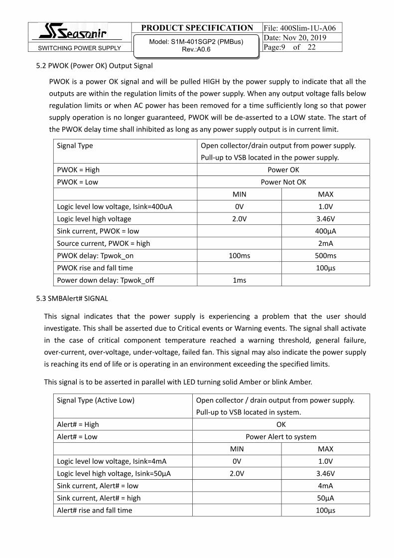
5.2 PWOK (Power OK) Output Signal
PWOK is a power OK signal and will be pulled HIGH by the power supply to indicate that all the outputs are within the regulation limits of the power supply. When any output voltage falls below regulation limits or when AC power has been removed for a time sufficiently long so that power supply operation is no longer guaranteed, PWOK will be de‐asserted to a LOW state. The start of the PWOK delay time shall inhibited as long as any power supply output is in current limit.
Signal Type Open collector/drain output from power supply. Pull‐up to VSB located in the power supply.
PWOK = High Power OK PWOK = Low Power Not OK MIN MAX Logic level low voltage, Isink=400uA 0V 1.0V Logic level high voltage 2.0V 3.46V Sink current, PWOK = low 400μA Source current, PWOK = high 2mA PWOK delay: Tpwok_on 100ms 500ms PWOK rise and fall time 100μs Power down delay: Tpwok_off 1ms
5.3 SMBAlert# SIGNAL
This signal indicates that the power supply is experiencing a problem that the user should investigate. This shall be asserted due to Critical events or Warning events. The signal shall activate in the case of critical component temperature reached a warning threshold, general failure, over‐current, over‐voltage, under‐voltage, failed fan. This signal may also indicate the power supply is reaching its end of life or is operating in an environment exceeding the specified limits.
This signal is to be asserted in parallel with LED turning solid Amber or blink Amber.
Signal Type (Active Low) Open collector / drain output from power supply. Pull‐up to VSB located in system.
Alert# = High OK Alert# = Low Power Alert to system MIN MAX Logic level low voltage, Isink=4mA 0V 1.0V Logic level high voltage, Isink=50μA 2.0V 3.46V Sink current, Alert# = low 4mA Sink current, Alert# = high 50μA Alert# rise and fall time 100μs
PRODUCT SPECIFICATION File: 400Slim-1U-A06 Date: Nov 20, 2019
SWITCHING POWER SUPPLY Page:10 of 22
Model: S1M-401SGP2 (PMBus) Rev.:A0.6
5.3.1 A0
PSU Module Address Line 0. This signal line is provided for determining the address for the specific PSU FRU and SMBus address. The pull‐up resister should be located in the system and the pull‐up voltage should be limited to 3.3V.
The address line should be pull low with equal to or less than 100ohm in the motherboard design.
5.3.2 A1
PSU Module Address Line 1. This signal line is provided for determining the address for the specific PSU FRU and SMBus address. The pull‐up resister should be located in the system and the pull‐up voltage should be limited to 3.3V.
The address line should be pull low with equal to or less than 100ohm in the motherboard design.
5.4 SDA and SCL
One pin is the serial clock (SCL), and the other pin is used for serial data (SDA). The SCL and SDA signals are pulled up by system, both pins are bi‐directional, open drain signals, and are used to form a serial bus.
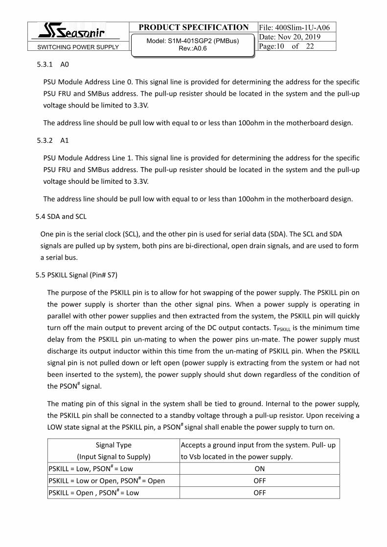
5.5 PSKILL Signal (Pin# S7)
The purpose of the PSKILL pin is to allow for hot swapping of the power supply. The PSKILL pin on the power supply is shorter than the other signal pins. When a power supply is operating in parallel with other power supplies and then extracted from the system, the PSKILL pin will quickly turn off the main output to prevent arcing of the DC output contacts. TPSKILL is the minimum time delay from the PSKILL pin un‐mating to when the power pins un‐mate. The power supply must discharge its output inductor within this time from the un‐mating of PSKILL pin. When the PSKILL signal pin is not pulled down or left open (power supply is extracting from the system or had not been inserted to the system), the power supply should shut down regardless of the condition of the PSON# signal.
The mating pin of this signal in the system shall be tied to ground. Internal to the power supply, the PSKILL pin shall be connected to a standby voltage through a pull‐up resistor. Upon receiving a LOW state signal at the PSKILL pin, a PSON# signal shall enable the power supply to turn on.
Signal Type (Input Signal to Supply)
Accepts a ground input from the system. Pull‐ up to Vsb located in the power supply.
PSKILL = Low, PSON# = Low ON PSKILL = Low or Open, PSON# = Open OFF PSKILL = Open , PSON# = Low OFF

PRODUCT SPECIFICATION File: 400Slim-1U-A06 Date: Nov 20, 2019
SWITCHING POWER SUPPLY Page:11 of 22
Model: S1M-401SGP2 (PMBus) Rev.:A0.6
MIN MAX Logic level low (power supply ON) 0V 1.0V Logic level high (power supply OFF) 2.0V 3.46V Source current, VPSKILL= low 2.8mA Delay from PSKILL=High to power supply turned off (TPSKILL)
100μsec
5.6 PRESENT Signal (Pin# S14)
This signal pin is recessed within the connector and will contact only once all other connector contacts are closed. This active‐low pin is used to indicate to a power distribution unit controller that a supply is plugged in. the maximum current on Present# pin should not exceed 10mA.
5.7 INPUT OK Signal (Pin# S19)
INPUT OK is an AC/HVDC OK signal and will be pulled up by the power supply to indicate that AC/HVDC input is within the operation range. The INPUT OK signal shall pull Lo < 2msec after input voltage is lost to 0V; after 4 AC cycles if the input voltage resume within operation range then INPUT OK signal shall pull High.
Signal Type Open collector / drain output from power supply. Pull‐up to VSB located in system.
Input OK = High The input Voltage meets the input range. Input OK = Lo The input Voltage doesn’t meet the input range. MIN MAX Logic level low voltage, Isink=4mA 0V 1.0V Logic level high voltage, Isink=200μA 2.0V 3.46V
6 Output Protection
6.1 Over Current Protection: (OCP)
This power supply has current limit to prevent the outputs from exceeding the values shown in table below. If the current limits are exceeded the power supply will shut down and latch off. The latch will be cleared by toggling the PSON# signal or by an AC power interruption. This power supply will not be damaged from repeated power cycling in this condition. +5VSB will be auto‐recovered after removing OCP limit.
Output VOLTAGE OVER CURRENT LIMITS +12V Peak current min; 110% of peak max +5VSB Min. 4A; Max. 6A.
PRODUCT SPECIFICATION File: 400Slim-1U-A06 Date: Nov 20, 2019
SWITCHING POWER SUPPLY Page:12 of 22
Model: S1M-401SGP2 (PMBus) Rev.:A0.6
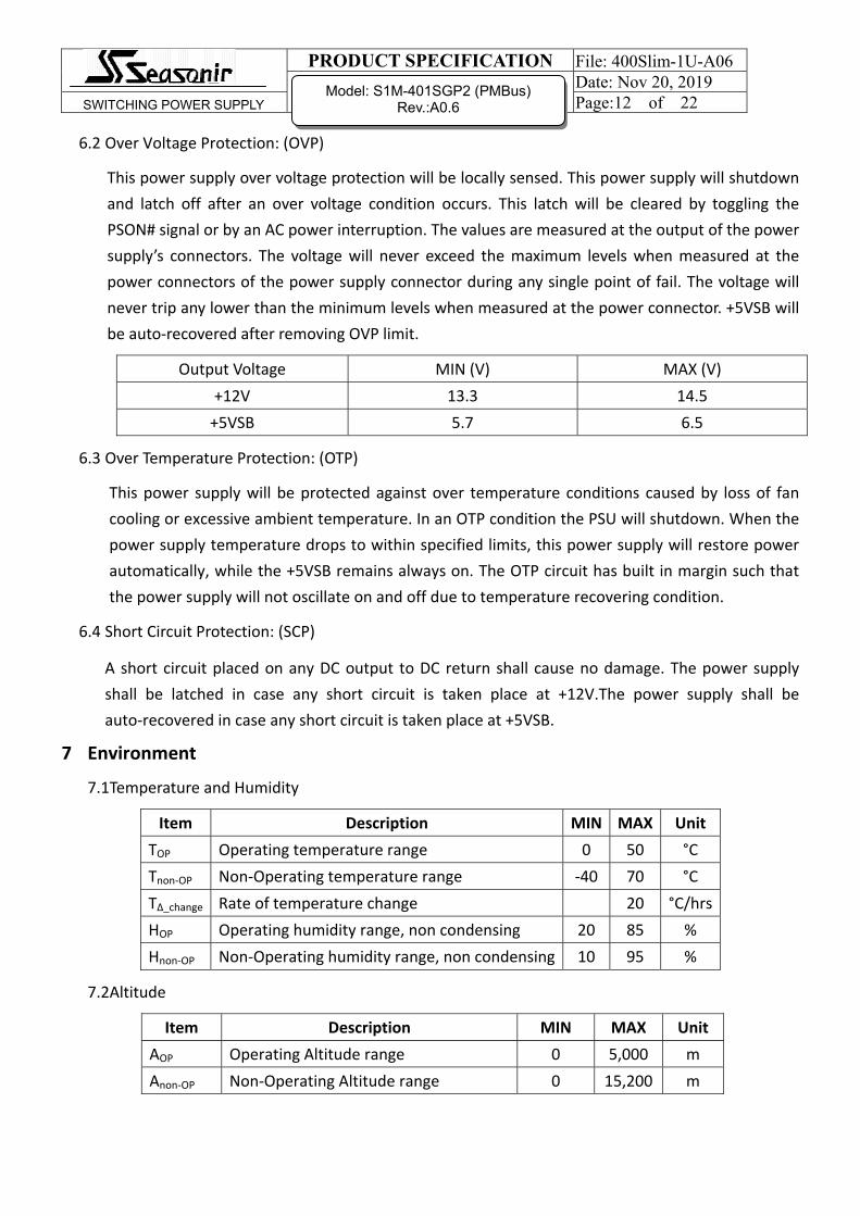
6.2 Over Voltage Protection: (OVP)
This power supply over voltage protection will be locally sensed. This power supply will shutdown and latch off after an over voltage condition occurs. This latch will be cleared by toggling the PSON# signal or by an AC power interruption. The values are measured at the output of the power supply’s connectors. The voltage will never exceed the maximum levels when measured at the power connectors of the power supply connector during any single point of fail. The voltage will never trip any lower than the minimum levels when measured at the power connector. +5VSB will be auto‐recovered after removing OVP limit.
Output Voltage MIN (V) MAX (V) +12V 13.3 14.5 +5VSB 5.7 6.5
6.3 Over Temperature Protection: (OTP)
This power supply will be protected against over temperature conditions caused by loss of fan cooling or excessive ambient temperature. In an OTP condition the PSU will shutdown. When the power supply temperature drops to within specified limits, this power supply will restore power automatically, while the +5VSB remains always on. The OTP circuit has built in margin such that the power supply will not oscillate on and off due to temperature recovering condition.
6.4 Short Circuit Protection: (SCP)
A short circuit placed on any DC output to DC return shall cause no damage. The power supply shall be latched in case any short circuit is taken place at +12V.The power supply shall be auto‐recovered in case any short circuit is taken place at +5VSB.
7 Environment
7.1Temperature and Humidity
Item Description MIN MAX Unit TOP Operating temperature range 0 50 °C Tnon‐OP Non‐Operating temperature range ‐40 70 °C TΔ_change Rate of temperature change 20 °C/hrsHOP Operating humidity range, non condensing 20 85 % Hnon‐OP Non‐Operating humidity range, non condensing 10 95 %
7.2Altitude
Item Description MIN MAX Unit AOP Operating Altitude range 0 5,000 m Anon‐OP Non‐Operating Altitude range 0 15,200 m

PRODUCT SPECIFICATION File: 400Slim-1U-A06 Date: Nov 20, 2019
SWITCHING POWER SUPPLY Page:13 of 22
Model: S1M-401SGP2 (PMBus) Rev.:A0.6
7.3 Random Vibration
Non‐operating
Sine sweep
5Hz to 500Hz @ 0.5gRMS at 0.5 octave/min; dwell 15 min at each of 3 resonant points;
Random profile
5Hz @ 0.01g²/Hz to 20Hz @ 0.02g²/Hz (slope up); 20Hz to 500Hz @ 0.02g²/Hz (flat);
Input acceleration = 3.13gRMS; 10 min. per axis for 3 axis on all samples
7.4Mechanical Shock
Operating: 5G, no malfunction Non‐operating: 50G, no damage. Trapezoidal Wave, Velocity change = 4.3m/sec. Three drops in each of six directions are applied to each of the samples
8 FRU Requirements
8.1 IPMI FRU Addressing
The PSU shall have an IPMI FRU (field replaceable unit). It shall be located at the following addresses.
This is intended to align with existing IPMI standards.
PSU IPMI FRU Device Address Locations Addresses used:
System addressing A1/ A0 3 0/0 0/1 1/0 1/1
FRU device read/write addresses 2 A0h/A1h 1 A2h/A3h A4h/A5h A6h/A7h
1 Non‐redundant power supplies will use the 0/0 address location. 2 The addressing method uses the 7 MSB bits to set the address and the LSB to define whether a device is reading or writing. The addresses defined above use 8 bits including the read/write bit. 3 The ‘0’ and ‘1’ correspond to ‘1’ = signal is not grounded; ‘0’ = signal is grounded
8.2 FRU Data
The FRU data format shall be compliant with the IPMI ver.1.0 (per rev.1.1 from Sept.25, 1999) specification. The current version of these specifications is available at
http:\\developer.intel.com/design/servers/ipmi/spec.htm
The following is the exact listing of the EEPROM content. During testing this listing shall be followed and verified.
PRODUCT SPECIFICATION File: 400Slim-1U-A06 Date: Nov 20, 2019
SWITCHING POWER SUPPLY Page:14 of 22
Model: S1M-401SGP2 (PMBus) Rev.:A0.6
8.2 FRU Device Protocol
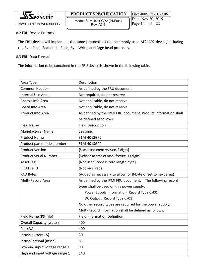
The FRU device will implement the same protocols as the commonly used AT24C02 device, including the Byte Read, Sequential Read, Byte Write, and Page Read protocols.
8.3 FRU Data Format
The information to be contained in the FRU device is shown in the following table.
Area Type Description Common Header As defined by the FRU document Internal Use Area Not required, do not reserve Chassis Info Area Not applicable, do not reserve Board Info Area Not applicable, do not reserve Product Info Area As defined by the IPMI FRU document. Product information shall
be defined as follows: Field Name Field Description Manufacturer Name Seasonic Product Name S1M‐401SGP2 Product part/model number S1M‐401SGP2 Product Version {Seasonic current revision, 3 digits} Product Serial Number {Defined at time of manufacture, 13 digits} Asset Tag {Not used, code is zero length byte} FRU File ID {Not required} PAD Bytes {Added as necessary to allow for 8‐byte offset to next area} Multi‐Record Area As defined by the IPMI FRU document. The following record
types shall be used on this power supply: Power Supply Information (Record Type 0x00) DC Output (Record Type 0x01) No other record types are required for the power supply. Multi‐Record information shall be defined as follows:
Field Name (PS Info) Field Information Definition Overall Capacity (watts) 400 Peak VA 400 Inrush current (A) 30 Inrush interval (msec) 5 Low end input voltage range 1 90 High end input voltage range 1 140
PRODUCT SPECIFICATION File: 400Slim-1U-A06 Date: Nov 20, 2019
SWITCHING POWER SUPPLY Page:15 of 22
Model: S1M-401SGP2 (PMBus) Rev.:A0.6
9 Firmware Requirements
9.1 PMBus
9.1.1 Addressing
The PSU PMBus device address locations are shown below. For redundant systems there are up to two signals
to set the address location of the PSU once it is installed in the system; Address1, Address0.
PSU PMBus Device Address Locations Addresses used: System addressing A1/ A0 3 0/0 0/1 1/0 1/1
PMBus device read / write addresses 2 B0h/B1h1 B2h/B3h B4h/B5h B6h/B7h
1 Non‐redundant power supplies will use the 0/0 address location 2 The addressing method uses the 7 MSB bits to set the address and the LSB to define whether a device is reading or writing. The addresses defined above use 8 bits including the read/write bit. 3 The ‘0’ and ‘1’ correspond to ‘1’ = signal is not grounded; ‘0’ = signal is grounded
9.1.2 PMBus Commands
The following PMBus commands shall be supported for the purpose of monitoring currents, voltages, and power. All sensors shall continue providing real time data as long as the PMBus device is powered. This means in standby mode the main output(s) of the power supply shall be zero amps and zero volts.
Command
Code Command Name SMBusb Transaction Type
Number Of Data
Bytes Data Format Remark
00h PAGE Read/Send Byte 1
03h CLEAR_FAULT Send Byte 0
Low end input voltage range 2 180 High end input voltage range 2 264 A/C dropout total. (msec) 10 Binary flags Set for: Hot Swap support, Auto switch, and PFC Peak Wattage 440 Combined wattage None Predictive fail tach support Supported Field Name (Output) Field Description: Two outputs are to be defined from #1 to #2,
as follows: +12V and +5VSB. Output Information Set for: Standby on +5VSB, No Standby on all others. All other output fields Format per IPMI specification, using parameters in this
specification.
PRODUCT SPECIFICATION File: 400Slim-1U-A06 Date: Nov 20, 2019
SWITCHING POWER SUPPLY Page:16 of 22
Model: S1M-401SGP2 (PMBus) Rev.:A0.6
05h PAGE_PLUS_WRITE Block Write Used with STATUS_INPUT, STATUS_TEMPERATURE,
STATUS_IOUT
06h PAGE_PLUS_READ Block Write-Block
Read Process Call
Used with STATUS_INPUT, STATUS_TEMPERATURE,
STATUS_IOUT, STATUS_WORD
19h CAPABILITY Read Byte 1
1Ah QUERY
Block Write-
Block Read
Process Call
1
1Bh SMBALERT_MASK
Write Word /Block
Write-
Block Read
Process Call
2
20h VOUT_MODE Read Byte 1
30h COEFFICIENTS
Block Write-
Block Read
Process Cal
5
3Ah FAN_CONFIG_1_2 Read Byte 1
3Bh FAN_COMMAND_1 Read/Write Word 2
78h STATUS_BYTE Read Byte 1
79h STATUS_WORD Read Word 2
7Ah STATUS_VOUT Read/Write Byte 1
7Bh STATUS_IOUT Read/Write Byte 1
7Dh STATUS_TEMPERATURE Read/Write Byte 1
7Eh STATUS_CML Read/Write Byte 1
7Fh STATUS_OTHER Read/Write Byte 1
81h STATUS_FAN_1_2 Read/Write Byte 1
86h READ_EIN Block Read 10
87h READ_EOUT Block Read 10
88h READ_VIN Read Word 2 Linear Data
Format
89h READ_IIN Read Word 2 Linear Data
Format
8Bh READ_VOUT Read Word 2 Linear Data
Format
8Ch READ_IOUT Read Word 2 Linear Data
Format
8Dh READ_TEMPERATURE_1 Read Word 2 Linear Data
PRODUCT SPECIFICATION File: 400Slim-1U-A06 Date: Nov 20, 2019
SWITCHING POWER SUPPLY Page:17 of 22
Model: S1M-401SGP2 (PMBus) Rev.:A0.6
Format
8Eh READ_TEMPERATURE_2 Read Word 2 Linear Data
Format
8Fh READ_TEMPERATURE_3 Read Word 2 Linear Data
Format
90h READ_FAN_SPEED_1 Read Word 2 Linear Data
Format
96h READ_POUT Read Word 2 Linear Data
Format
97h READ_PIN Read Word 2 Linear Data
Format
98h PMBUS_REVISION Read Byte 1
99h MFR_ID Block Read Variable(up to
32 bytes) ASCII only Block Read for users
9Ah MFR_MODEL Block Read Variable(up to
32 bytes) ASCII only Block Read for users
9Bh MFR_REVISION Block Read Variable(up to
32 bytes) ASCII only Block Read for users
9Ch MFR_LOCATION Block Read Variable(up to
32 bytes) ASCII only Block Read for users
9Dh MFR_DATE Block Read Variable(up to
32 bytes) ASCII only Block Read for users
9Eh MFR_SERIAL Block Read Variable(up to
32 bytes) ASCII only Block Read for users
A0h MFR_VIN_MIN Read Word 2 Linear Data
Format
A1h MFR_VIN_MAX Read Word 2 Linear Data
Format
A2h MFR_IIN_MAX Read Word 2 Linear Data
Format
A3h MFR_PIN_MAX Read Word 2 Linear Data
Format
A4h MFR_VOUT_MIN Read Word 2 Linear Data
Format
A5h MFR_VOUT_MAX Read Word 2 Linear Data
Format
A6h MFR_IOUT_MAX Read Word 2 Linear Data
PRODUCT SPECIFICATION File: 400Slim-1U-A06 Date: Nov 20, 2019
SWITCHING POWER SUPPLY Page:18 of 22
Model: S1M-401SGP2 (PMBus) Rev.:A0.6
Format
A7h MFR_POUT_MAX Read Word 2 Linear Data
Format
A8h MFR_TAMBIENT_MAX Read Word 2 Linear Data
Format
A9h MFR_TAMBIENT_MIN Read Word 2 Linear Data
Format
ABh MFR_EFFICIENCY_HL Block Read 14
D0h MFR_REDUNDANCY_SETTING Read/Write Byte 1
DCh MFR_BLACK_BOX Block Read 230
DDh MFR_REAL_TIME_BLACK_BOX Block Write / Block
Read 4
DEh MFR_SYSTEM_BLACK_BOX Block Write / Block
Read 40
DFh MFR_BLACK_BOX_CONFIG Read/Write Byte 1
E0h MFR_CLEAR_BLACK_BOX Send Byte 0
FBh MFR_PFC_FIRMWARE_VERSION Read Word 2 Mfr
FCh MFR_SND_FIRMWARE_VERSION Read Word 2 Mfr
9.2 Sensors Accuracy
Sensor Functions Accuracy
0‐100% load
Accuracy
40‐200W load
Accuracy
200W‐Full load
READ_VIN +/‐ 3%
READ_IIN +/‐ 5%
READ_PIN +/‐ 10W +/‐ 5%
READ_VOUT +/‐ 3%
READ_IOUT +/‐ 1A +/‐ 5%
READ_POUT +/‐ 10W +/‐ 5%
READ_TEMPERATURE +/‐ 3 °C
READ_FAN_SPEED +/‐ 5 %
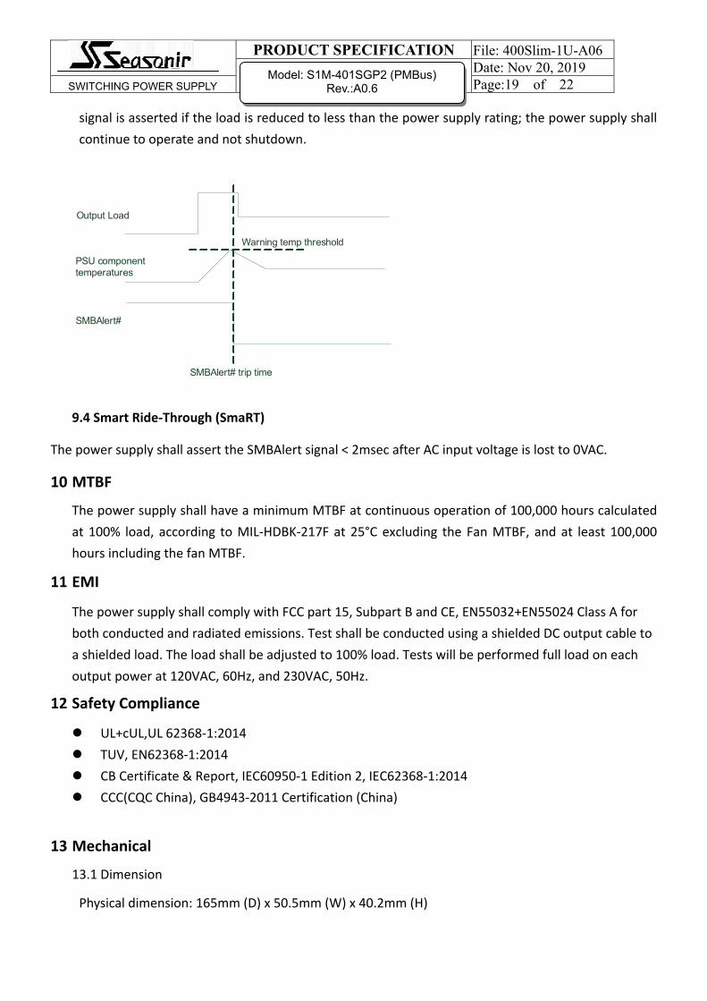
9.3 Closed Loop System Throttling (CLST)
The power supply shall always assert the SMBAlert signal whenever any component in the power supply reaches a warning threshold. Upon reduction of the load within 2msec after the SMBlert#
PRODUCT SPECIFICATION File: 400Slim-1U-A06 Date: Nov 20, 2019
SWITCHING POWER SUPPLY Page:19 of 22
Model: S1M-401SGP2 (PMBus) Rev.:A0.6
signal is asserted if the load is reduced to less than the power supply rating; the power supply shall continue to operate and not shutdown.
Output Load
PSU component temperatures
SMBAlert#
Warning temp threshold
SMBAlert# trip time
9.4 Smart Ride‐Through (SmaRT)
The power supply shall assert the SMBAlert signal < 2msec after AC input voltage is lost to 0VAC.
10 MTBF
The power supply shall have a minimum MTBF at continuous operation of 100,000 hours calculated at 100% load, according to MIL‐HDBK‐217F at 25°C excluding the Fan MTBF, and at least 100,000 hours including the fan MTBF.
11 EMI
The power supply shall comply with FCC part 15, Subpart B and CE, EN55032+EN55024 Class A for both conducted and radiated emissions. Test shall be conducted using a shielded DC output cable to a shielded load. The load shall be adjusted to 100% load. Tests will be performed full load on each output power at 120VAC, 60Hz, and 230VAC, 50Hz.
12 Safety Compliance
z UL+cUL,UL 62368‐1:2014 z TUV, EN62368‐1:2014 z CB Certificate & Report, IEC60950‐1 Edition 2, IEC62368‐1:2014 z CCC(CQC China), GB4943‐2011 Certification (China)
13 Mechanical
13.1 Dimension
Physical dimension: 165mm (D) x 50.5mm (W) x 40.2mm (H)

PRODUCT SPECIFICATION File: 400Slim-1U-A06 Date: Nov 20, 2019
SWITCHING POWER SUPPLY Page:20 of 22
Model: S1M-401SGP2 (PMBus) Rev.:A0.6
13.2 DC output connector
The power supply has a card edge for the DC outputs and signal pins, mating with Molex LPH series connector on the PDB side. DC output pin definitions shown as below table.
Pin# Signal Name Function S1 +12VRS+ +12V remote sense S2 +12VRS‐ +12V RTN sense S3 12V LS Current share bus S4 SMB ALERT Failure notification S5 SDA I2C Data signal S6 SCL I2C Clock signal S7 PSKILL PSU off signal S8 PSON Power enable input S9 PWOK Power output S10 A1 I2C address bit 1 S11 +5Vsb +5Vsb output S12 +5Vsb +5Vsb output S13 N/A N/A S14 PRESENT PSU present S15 A0 I2C address bit 0 S16 N/A N/A S17 N/A N/A S18 N/A N/A S19 INPUT OK Input present signal S20 N/A N/A S21 CR_BUS Cold Redundancy Bus S22 N/A N/A S23 +5Vsb +5Vsb output S24 +5Vsb +5Vsb output P1 +12V +12V P2 +12V +12V P3 SGND GND P4 SGND GND
PRODUCT SPECIFICATION File: 400Slim-1U-A06 Date: Nov 20, 2019
SWITCHING POWER SUPPLY Page:21 of 22
Model: S1M-401SGP2 (PMBus) Rev.:A0.6
14 Redundant Function 14.1 Hot Swap Requirements
Hot Swapping a power supply is the process of inserting and extracting a power supply from an operating power system. During this process the output voltages shall remain within the limits with the capacitive load specified. The hot swap test must be conducted when the system is operating under static, dynamic and zero loading conditions. The power supply can be hot swapped by the following method:
Extraction: The power supply may be removed from the system while operating with PSON# asserted, while in standby mode with PSON# de‐asserted or with no AC applied. No connector damage should occur during un‐mating of the power supply from the power distribution board (PDB).
Insertion: The power supply may be inserted into the system with PSON# asserted, with PSON# de‐asserted or with no AC power present for that supply. No connector damage should occur due to the mating of the output and input connector.
In general a failed (of by internal latch or external control) supply may be removed, then replaced with a good power supply, however, hot swap needs to work with operational as well as failed power supplies. The newly inserted power supply will get turned on into standby or Power On mode once inserted.
14.2 LED Indicators
The power supply uses a bi‐color LED; Amber & Green. Below are table showing the LED states for power supply operating state.
Power Supply Condition LED State
Output ON and OK GREEN
No AC power to all power supplies OFF
PSU standby state AC present / Only Standby on
1Hz Blink GREEN
Power supply critical event causing a shutdown; failure, over current, short circuit, over voltage, fan failure, over temperature
AMBER
PRODUCT SPECIFICATION File: 400Slim-1U-A06 Date: Nov 20, 2019
SWITCHING POWER SUPPLY Page:22 of 22
Model: S1M-401SGP2 (PMBus) Rev.:A0.6
15 Fan and Fan Speed Control
This power supply incorporates a 40mm fan for cooling the power supply. When installed in the system, the airflow direction shall be from the card edge connector side to the AC inlet side of the power supply.
The fan speed control has close loop algorithm based on both the critical component temperature and the ambient temperature (Inlet temperature). The PSU fan always ramps to maximum speed under any condition to protect the power supply from overheating and the acoustic level will be >57dBA. These conditions include high ambient temperatures, loading, AC input, and airflow impedance.


![HDU 6WHOOD 'HVLJQ$UWLFOH GHVFULSWLRQ1XPEHU … · /lodf 1u p /lolnrl 1u p /loo\ 1u p oltxrulfh 1u p /l]dug 1u p /rwxv 1u p 0d\ 1u p 3djh ri 0lgqljkw 1u p 0lprvd 1u p 0rrqvwuxfn 1u](https://img.pdfslide.us/doc/110x75/5c02823709d3f252338e3217/hdu-6whood-hvljquwlfoh-ghvfulswlrq1xpehu-lodf-1u-p-lolnrl-1u-p-loo-1u.jpg)


![Scientific Programming [24pt] Lecture A06 Recursion](https://img.pdfslide.us/doc/110x75/61ef743efe823b3a1253a364/scientific-programming-24pt-lecture-a06-recursion.jpg)