Embed Size (px)
Citation preview
1www.fciconnect.com TRX10GDL0610 Datasheet, Rev C1-01, July 2010
TRANSCEIVERS
Product Specification10GBd SFP+ 1310nm LRM Linear TransceiverTRX10GDL0610
APPLICATIONS
10G Ethernet 10GBASE-LRM
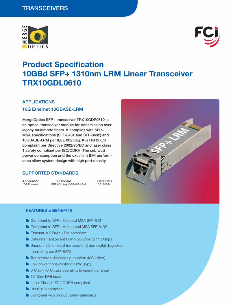
MergeOptics SFP+ transceiver TRX10GDP0610 is an optical transceiver module for transmission over legacy multimode fibers. It complies with SFP+ MSA specifications (SFF-8431 and SFF-8432) and 10GBASE-LRM per IEEE 802.3aq. It is RoHS 6/6 complaint per Directive 2002/95/EC and laser class 1 safety compliant per IEC/CDRH. The sub watt power consumption and the excellent EMI perform-ance allow system design with high port density.
SUPPORTED STANDARDS
Application Standard Data Rate10G Ethernet IEEE 802.3aq 10GBASE-LRM 10.3125GBd
FEATURES & BENEFITS
Compliant to SFP+ Electrical MSA SFF-8431
Compliant to SFP+ Mechanical MSA SFF-8432
Ethernet 10GBase-LRM compliant
Data rate transparent from 9.95Gbps to 11.3Gbps
Support I2C for serial transceiver ID and digital diagnostic
monitoring per SFF-8472.
Transmission distance up to 220m (MO1 fiber)
Low power consumption: 0.8W (Typ.)
0°C to +70°C case operating temperature range
1310nm DFB laser
Laser Class 1 IEC / CDRH compliant
RoHS 6/6 compliant
Compliant with product safety standards
2www.fciconnect.com TRX10GDL0610 Datasheet, Rev C1-01, July 2010
Product Specification10GBd SFP+ 1310nm LRM Linear Transceiver TRX10GDL06100
TABLE OF CONTENTS
Table of Contents 2
Functional Description 3
Electrical Characteristics 4
Absolute Maximum Ratings 4
Recommended Operating Conditions 4
Low Speed Characteristics 4
SFI Module Transmitter Input Characteristics 5
SFI Module Receiver Output Characteristics 5
Optical Characteristics 6
General Parameters 6
Optical Transmitter 6
Optical Receiver 6
Application Information 7
Connector Pinout 7
Electrical Pin Definition 7
Application Schematics 8
Interfacing the Transceiver 9
Digital Diagnostic Monitoring 9
Digital Diagnostic Monitoring Accuracy 9
Module Outline 10
Ordering Information 10
Regulatory Compliance 11
Module Safety 11
ESD & Electromagnetic compatibility 11
Eye Safety 11
Sales Contacts 12
3www.fciconnect.com TRX10GDL0610 Datasheet, Rev C1-01, July 2010
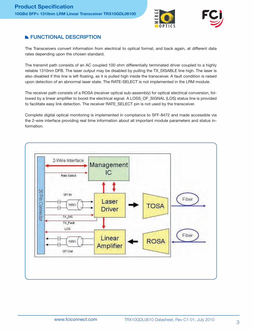
FUNCTIONAL DESCRIPTION
The Transceivers convert information from electrical to optical format, and back again, at different data rates depending upon the chosen standard.
The transmit path consists of an AC coupled 100 ohm differentially terminated driver coupled to a highly reliable 1310nm DFB. The laser output may be disabled by pulling the TX_DISABLE line high. The laser is also disabled if this line is left floating, as it is pulled high inside the transceiver. A fault condition is raised upon detection of an abnormal laser state. The RATE-SELECT is not implemented in the LRM module.
The receiver path consists of a ROSA (receiver optical sub-assembly) for optical electrical conversion, fol-lowed by a linear amplifier to boost the electrical signal. A LOSS_OF_SIGNAL (LOS) status line is provided to facilitate easy link detection. The receiver RATE_SELECT pin is not used by the transceiver.
Complete digital optical monitoring is implemented in compliance to SFF-8472 and made accessible via the 2-wire interface providing real time information about all important module parameters and status in-formation.
Product Specification10GBd SFP+ 1310nm LRM Linear Transceiver TRX10GDL06100
4www.fciconnect.com TRX10GDL0610 Datasheet, Rev C1-01, July 2010
ELECTRICAL CHARACTERISTICS
Product Specification10GBd SFP+ 1310nm LRM Linear Transceiver TRX10GDL06100
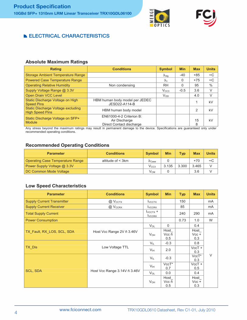
Absolute Maximum Ratings
Rating Conditions Symbol Min Max Units
Storage Ambient Temperature Range ϑstg -40 +85 ∞C
Powered Case Temperature Range ϑc 0 +75 ∞C
Operating Relative Humidity Non condensing RH 0 95 %
Supply Voltage Range @ 3.3V VCC3 -0.5 3.6 V
Open Drain VCC Level VOD 4.0 V
Static Discharge Voltage on High Speed Pins
HBM human body model per JEDEC JESD22-A114-B
1 kV
Static Discharge Voltage excluding High Speed Pins
HBM human body model 2 kV
Static Discharge Voltage on SFP+Module
EN61000-4-2 Criterion B: Air Discharge
Direct Contact discharge158
kV
Any stress beyond the maximum ratings may result in permanent damage to the device. Specifications are guaranteed only under recommended operating conditions.
Recommended Operating Conditions
Parameter Conditions Symbol Min Typ Max Units
Operating Case Temperature Range altitude of < 3km ϑCase 0 +70 ∞C
Power Supply Voltage @ 3.3V VCC3 3.135 3.300 3.465 V
DC Common Mode Voltage VCM 0 3.6 V
Low Speed Characteristics
Parameter Conditions Symbol Min Typ Max Units
Supply Current Transmitter @ VCCTX IVCCTX 150 mA
Supply Current Receiver @ VCCRX IVCCRX 85 mA
Total Supply CurrentIVCCTX +IVCCRX
240 290 mA
Power Consumption 0.73 1.0 W
TX_Fault, RX_LOS, SCL, SDA Host Vcc Range 2V ñ 3.46V
VOL 0 0.4
V
VOH
Host_Vcc ñ
0.5
Host_Vcc +
0.3
TX_Dis Low Voltage TTL
VIL -0.3 0.8
VIH 2.0VccT +
0.3
SCL, SDA Host Vcc Range 3.14V ñ 3.46V
VIL -0.3VccT*
0.3
VIHVccT*
0.7VccT +
0.5
VOL 0.0 0.4
VOH
Host_Vcc ñ
0.5
Host_Vcc +
0.3
5www.fciconnect.com TRX10GDL0610 Datasheet, Rev C1-01, July 2010
FUNCTIONAL DESCRIPTION
Product Specification10GBd SFP+ 1310nm LRM Linear Transceiver TRX10GDL06100
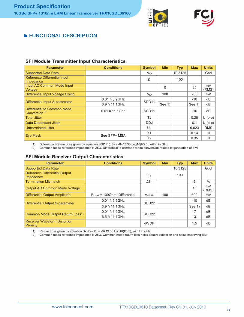
SFI Module Transmitter Input Characteristics
Parameter Conditions Symbol Min Typ Max Units
Supported Data Rate VID 10.3125 Gbd
Reference Differential Input Impedance
Zd 100
Input AC Common Mode Input Voltage
0 25mV
(RMS)
Differential Input Voltage Swing VID 180 700 mV
Differential Input S-parameter0.01 ñ 3.9GHz
SDD11-10 dB
3.9 ñ 11.1GHz See 1) See 1) dB
Differential to Common Mode Conversion
2) 0.01 ñ 11.1Ghz SCD11 -10 dB
Total Jitter TJ 0.28 UI(p-p)
Data Dependant Jitter DDJ 0.1 UI(p-p)
Uncorrelated Jitter UJ 0.023 RMS
Eye Mask See SFP+ MSAX1 0.14 UI
X2 0.35 UI
1) Differential Return Loss given by equation SDD11(dB) = -8+13.33 Log10(f/5.5), with f in GHz2) Common mode reference impedance is 25 . Differential to common mode conversion relates to generation of EMI
SFI Module Receiver Output Characteristics
Parameter Conditions Symbol Min Typ Max Units
Supported Data Rate 10.3125 Gbd
Reference Differential Output Impedance
Zd 100
Termination Mismatch d 5 %
Output AC Common Mode Voltage 15mV
(RMS)
Differential Output Amplitude RLoad = 100Ohm, Differential VOSPP 180 600 mV
Differential Output S-parameter0.01 ñ 3.9GHz
SDD22-10 dB
3.9 ñ 11.1GHz See 1) dB
Common Mode Output Return Loss2)
0.01 ñ 6.5GHzSCC22
-7 dB
6.5 ñ 11.1GHz -3 dB
Receiver Waveform Distortion Penalty
dWDP 1.5 dB
1) Return Loss given by equation Sxx22(dB) = -8+13.33 Log10(f/5.5), with f in GHz2) Common mode reference impedance is 25 . Common mode return loss helps absorb reflection and noise improving EMI
6www.fciconnect.com TRX10GDL0610 Datasheet, Rev C1-01, July 2010
OPTICAL CHARACTERISTICS
Product Specification10GBd SFP+ 1310nm LRM Linear Transceiver TRX10GDL06100
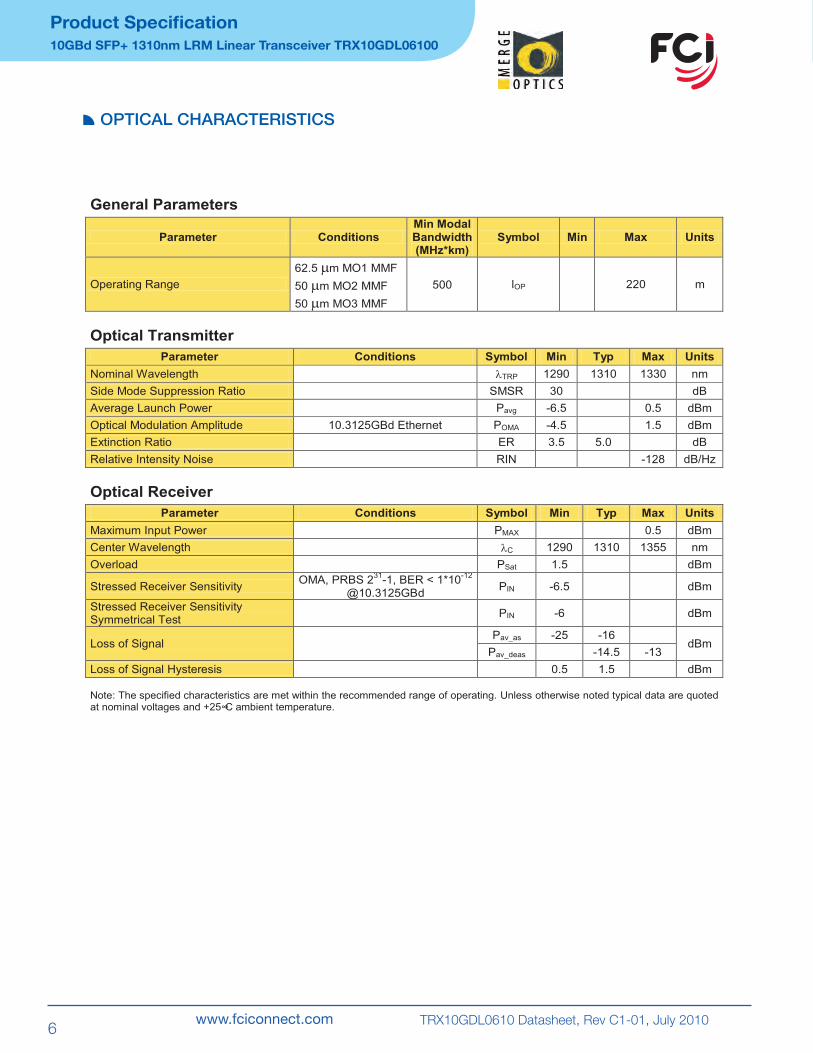
General Parameters
Parameter ConditionsMin Modal Bandwidth(MHz*km)
Symbol Min Max Units
Operating Range
62.5 µm MO1 MMF
50 µm MO2 MMF
50 µm MO3 MMF
500 lOP 220 m
Optical Transmitter
Parameter Conditions Symbol Min Typ Max Units
Nominal Wavelength λTRP 1290 1310 1330 nm
Side Mode Suppression Ratio SMSR 30 dB
Average Launch Power Pavg -6.5 0.5 dBm
Optical Modulation Amplitude 10.3125GBd Ethernet POMA -4.5 1.5 dBm
Extinction Ratio ER 3.5 5.0 dB
Relative Intensity Noise RIN -128 dB/Hz
Optical Receiver
Parameter Conditions Symbol Min Typ Max Units
Maximum Input Power PMAX 0.5 dBm
Center Wavelength λC 1290 1310 1355 nm
Overload PSat 1.5 dBm
Stressed Receiver SensitivityOMA, PRBS 2
31-1, BER < 1*10
-12
@10.3125GBdPIN -6.5 dBm
Stressed Receiver SensitivitySymmetrical Test
PIN -6 dBm
Loss of SignalPav_as -25 -16
dBmPav_deas -14.5 -13
Loss of Signal Hysteresis 0.5 1.5 dBm
Note: The specified characteristics are met within the recommended range of operating. Unless otherwise noted typical data are quoted at nominal voltages and +25∞C ambient temperature.
7www.fciconnect.com TRX10GDL0610 Datasheet, Rev C1-01, July 2010
APPLICATION INFORMATION
Product Specification10GBd SFP+ 1310nm LRM Linear Transceiver TRX10GDL06100
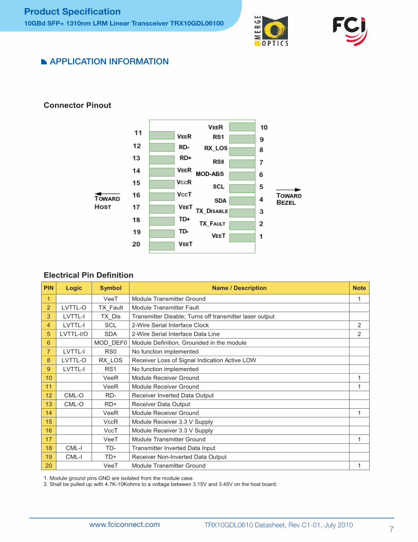
Connector Pinout
Electrical Pin Definition
PIN Logic Symbol Name / Description Note
1 VeeT Module Transmitter Ground 1
2 LVTTL-O TX_Fault Module Transmitter Fault
3 LVTTL-I TX_Dis Transmitter Disable; Turns off transmitter laser output
4 LVTTL-I SCL 2-Wire Serial Interface Clock 2
5 LVTTL-I/O SDA 2-Wire Serial Interface Data Line 2
6 MOD_DEF0 Module Definition, Grounded in the module
7 LVTTL-I RS0 No function implemented
8 LVTTL-O RX_LOS Receiver Loss of Signal Indication Active LOW
9 LVTTL-I RS1 No function implemented
10 VeeR Module Receiver Ground 1
11 VeeR Module Receiver Ground 1
12 CML-O RD- Receiver Inverted Data Output
13 CML-O RD+ Receiver Data Output
14 VeeR Module Receiver Ground 1
15 VccR Module Receiver 3.3 V Supply
16 VccT Module Receiver 3.3 V Supply
17 VeeT Module Transmitter Ground 1
18 CML-I TD- Transmitter Inverted Data Input
19 CML-I TD+ Receiver Non-Inverted Data Output
20 VeeT Module Transmitter Ground 1
1. Module ground pins GND are isolated from the module case.2. Shall be pulled up with 4.7K-10Kohms to a voltage between 3.15V and 3.45V on the host board.
8www.fciconnect.com TRX10GDL0610 Datasheet, Rev C1-01, July 2010
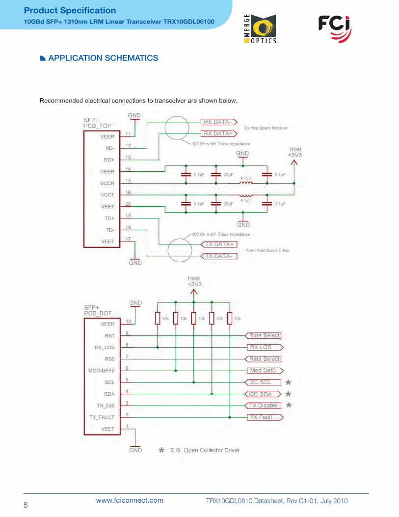
APPLICATION SCHEMATICS
Product Specification10GBd SFP+ 1310nm LRM Linear Transceiver TRX10GDL06100
Recommended electrical connections to transceiver are shown below.
9www.fciconnect.com TRX10GDL0610 Datasheet, Rev C1-01, July 2010
INTERFACING THE TRANSCEIVER
Product Specification10GBd SFP+ 1310nm LRM Linear Transceiver TRX10GDL06100
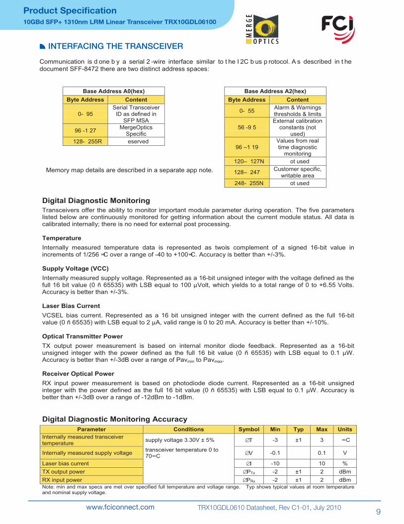
Communication is d one b y a serial 2 -wire interface similar to t he I 2C b us p rotocol. A s described in t he document SFF-8472 there are two distinct address spaces:
Base Address A0(hex)Byte Address Content
0- 95Serial Transceiver
ID as defined in SFP MSA
96 -1 27 MergeOptics Specific
128- 255R eserved
Memory map details are described in a separate app note.
Base Address A2(hex)Byte Address Content
0- 55 Alarm & Warnings thresholds & limits
56 -9 5External calibration
constants (not used)
96 –1 19Values from real time diagnostic
monitoring120– 127N ot used
128– 247 Customer specific, writable area
248- 255N ot used
Digital Diagnostic Monitoring
Transceivers offer the ability to monitor important module parameter during operation. The five parameters listed below are continuously monitored for getting information about the current module status. All data is calibrated internally; there is no need for external post processing.
Temperature
Internally measured temperature data is represented as twoís complement of a signed 16-bit value inincrements of 1/256 ∞C over a range of -40 to +100∞C. Accuracy is better than +/-3%.
Supply Voltage (VCC)
Internally measured supply voltage. Represented as a 16-bit unsigned integer with the voltage defined as the full 16 bit value (0 ñ 65535) with LSB equal to 100 Volt, which yields to a total range of 0 to +6.55 Volts.Accuracy is better than +/-3%.
Laser Bias Current
VCSEL bias current. Represented as a 16 bit unsigned integer with the current defined as the full 16-bit value (0 ñ 65535) with LSB equal to 2 A, valid range is 0 to 20 mA. Accuracy is better than +/-10%.
Optical Transmitter Power
TX output power measurement is based on internal monitor diode feedback. Represented as a 16-bit unsigned integer with the power defined as the full 16 bit value (0 ñ 65535) with LSB equal to 0.1 W. Accuracy is better than +/-3dB over a range of Pavmin to Pavmax.
Receiver Optical Power
RX input power measurement is based on photodiode diode current. Represented as a 16-bit unsigned integer with the power defined as the full 16 bit value (0 ñ 65535) with LSB equal to 0.1 W. Accuracy is better than +/-3dB over a range of -12dBm to -1dBm.
Digital Diagnostic Monitoring Accuracy
Parameter Conditions Symbol Min Typ Max Units
Internally measured transceiver temperature
supply voltage 3.30V ± 5% ∅T -3 ±1 3 ∞C
Internally measured supply voltagetransceiver temperature 0 to 70∞C
∅V -0.1 0.1 V
Laser bias current ∅I -10 10 %
TX output power ∅PTx -2 ±1 2 dBm
RX input power ∅PRx -2 ±1 2 dBm
Note: min and max specs are met over specified full temperature and voltage range. Typ shows typical values at room temperature and nominal supply voltage.
10www.fciconnect.com TRX10GDL0610 Datasheet, Rev C1-01, July 2010
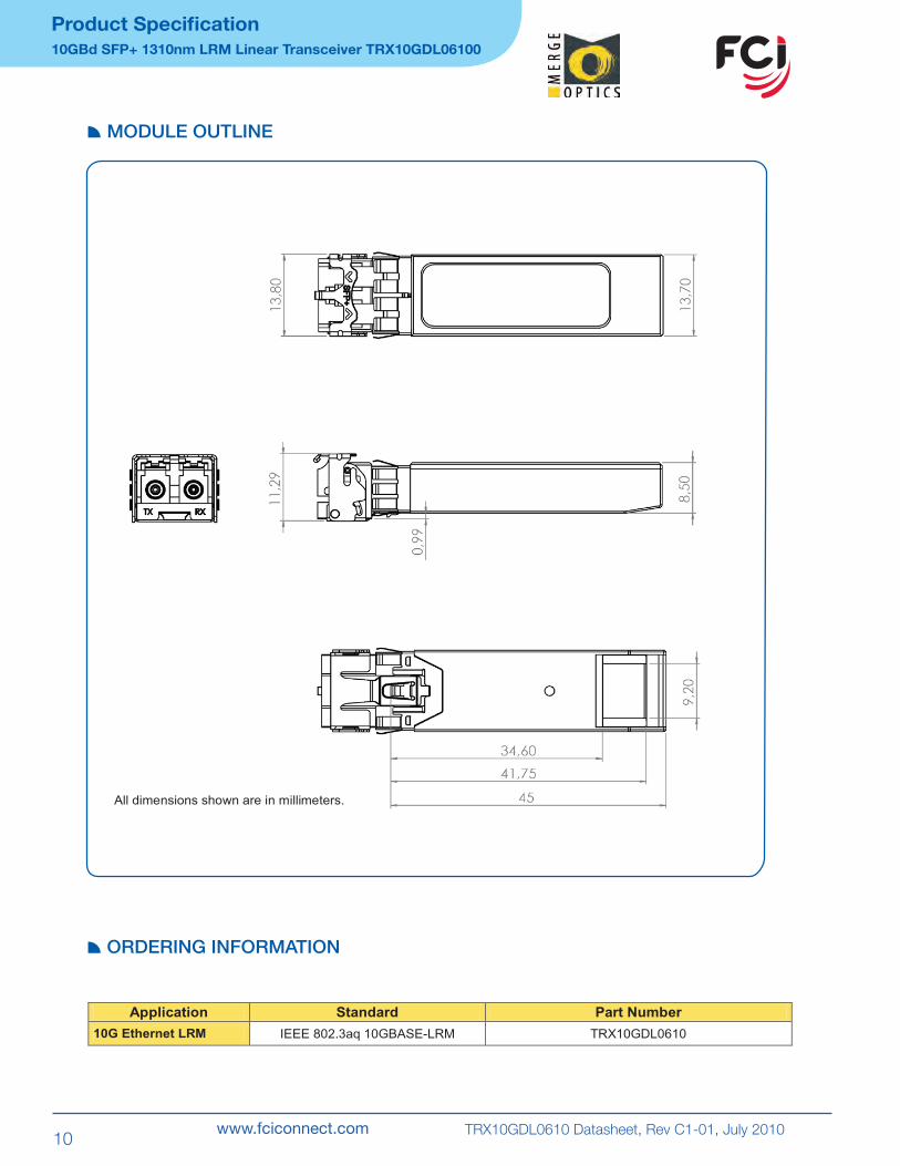
MODULE OUTLINE
ORDERING INFORMATION
Product Specification10GBd SFP+ 1310nm LRM Linear Transceiver TRX10GDL06100
All dimensions shown are in millimeters.
11www.fciconnect.com TRX10GDL0610 Datasheet, Rev C1-01, July 2010
REGULATORY COMPLIANCE
EYE SAFETY
Product Specification10GBd SFP+ 1310nm LRM Linear Transceiver TRX10GDL06100

12www.fciconnect.com TRX10GDL0610 Datasheet, Rev C1-01, July 2010
For more information about e-catalog or FCIsales offices, headquarters, agents and local distributors,
visit www.fciconnect.com
EUROPE
FCI Deutschland GmbH
Wernerwerkdamm 16 13629 Berlin, Germany Ph: +49 30 750 795 00 Fax: +49 30 386 37 54
AMERICAS
MergeOptics 1551 McCarthy Blvd, Suite 116 Milpitas, CA 95035 USA Phone: 408-493-9970
More information about FCI’s complete range of High Speed Input/Output products can be found on www.fciconnect.com/hsio
Contact info
ELX
10G
DL0
6107
10E
LT
Prin
ted
on
recy
cled
pap
er