Embed Size (px)
Citation preview
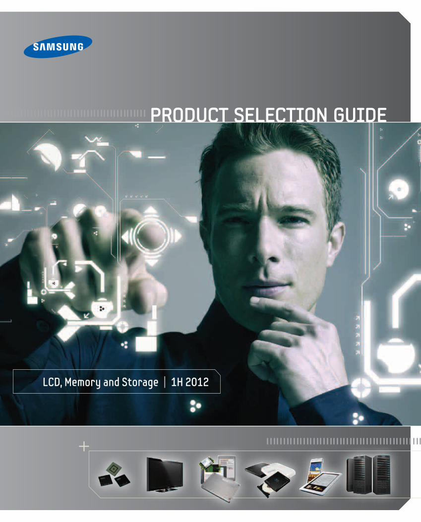
PRODUCT SELECTION GUIDE
LCD, Memory and Storage | 1H 2012
+
Samsung Semiconductor, Inc.
samsung.com/us/oem-solutions
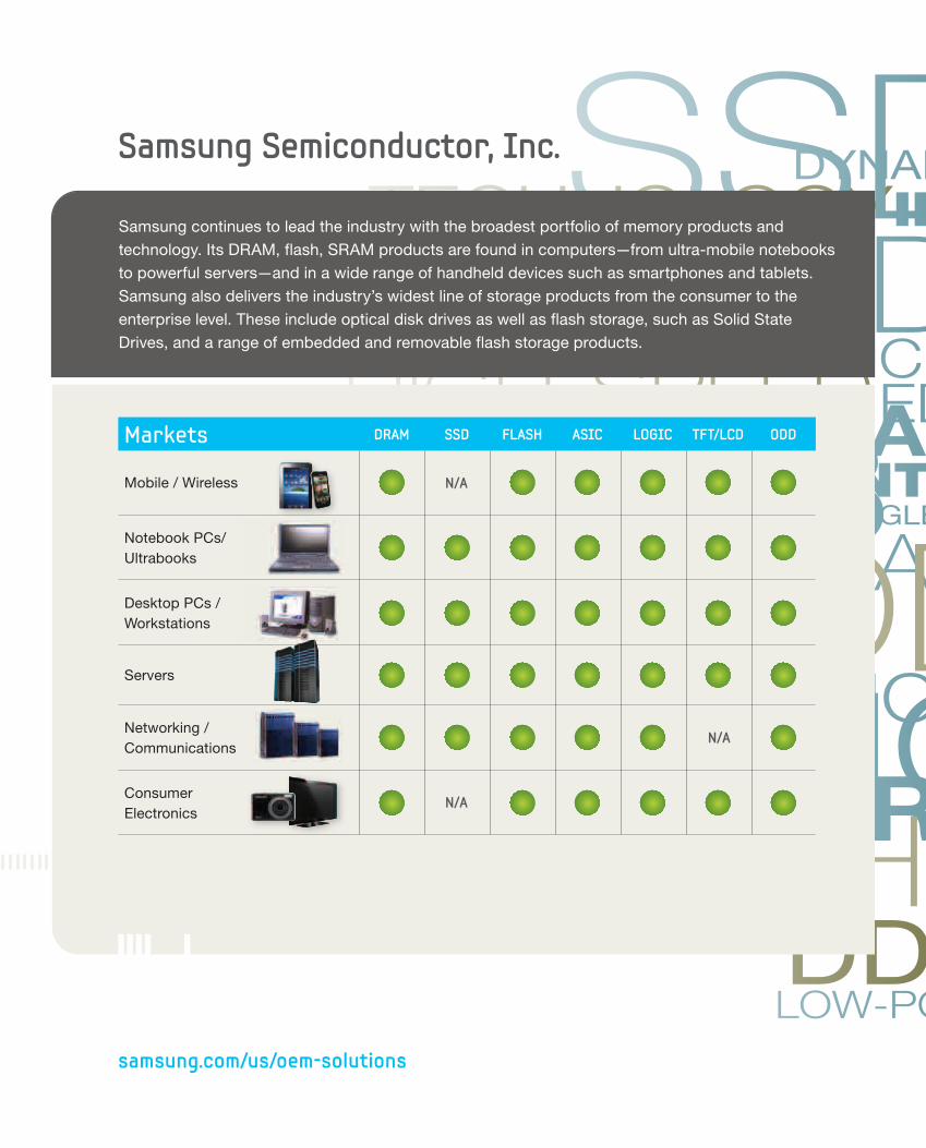
Mobile / Wireless
Notebook PCs/Ultrabooks
Desktop PCs /Workstations
Servers
Networking / Communications
Consumer Electronics
Markets DRAM SSD FLASH ASIC LOGIC TFT/LCD ODD
Samsung continues to lead the industry with the broadest portfolio of memory products and technology. Its DRAM, flash, SRAM products are found in computers—from ultra-mobile notebooks to powerful servers—and in a wide range of handheld devices such as smartphones and tablets. Samsung also delivers the industry’s widest line of storage products from the consumer to the enterprise level. These include optical disk drives as well as flash storage, such as Solid State Drives, and a range of embedded and removable flash storage products.
N/A
N/A
N/A
samsung.com/semi/dram 3
DR
AM
1H 2012
• DDR3 SDRAM• DDR2 SDRAM• DDR SDRAM• SDRAM
• Mobile DRAM• Graphics DDR SDRAM• DRAM Ordering
Information
• SLC Flash• MLC Flash• SD and microSD Cards• moviNAND™ (eMMC)
• Solid State Drive• Flash Ordering
Information
• NAND + MDDR• moviNAND + LPDDR2• NOR + UtRAM
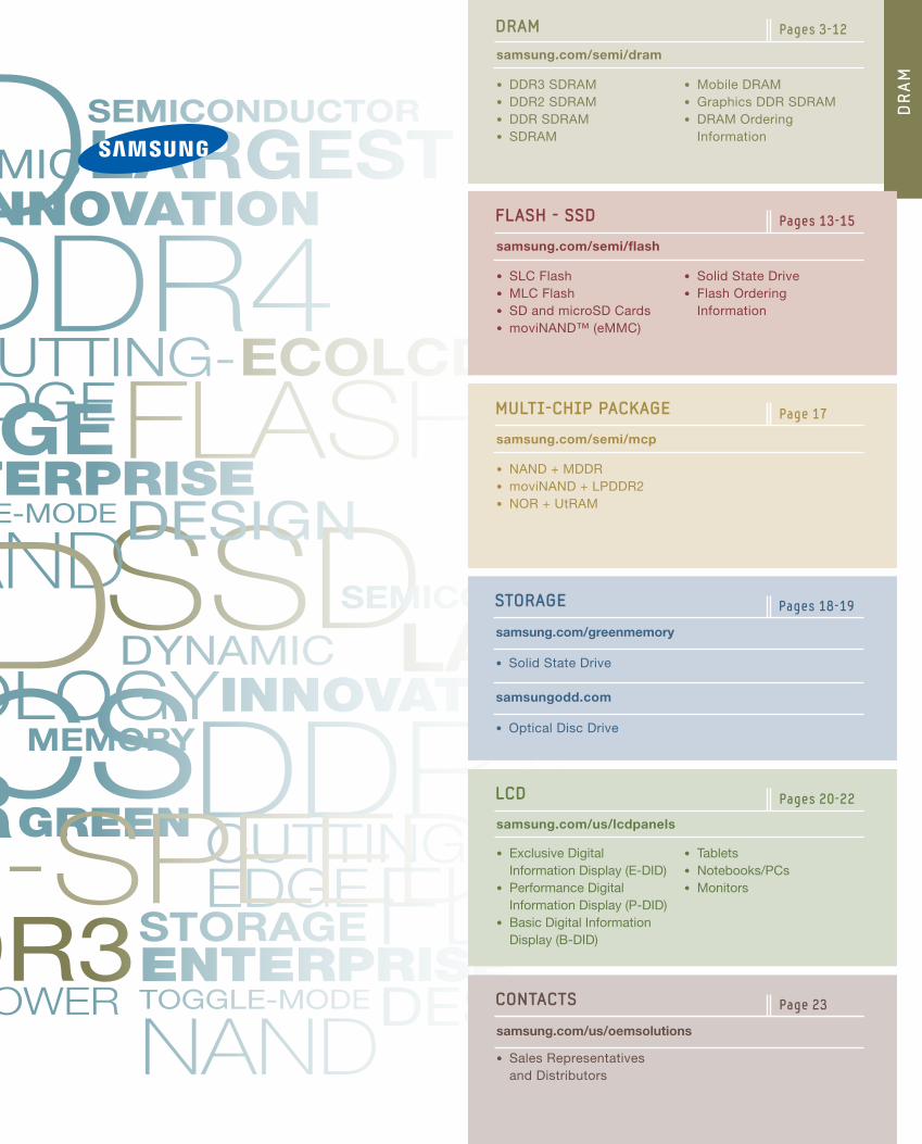
Pages 3-12
Pages 13-15
Page 17
Pages 20-22
Page 23
DRAM
FLASH - SSD
MULTI-CHIP PACKAGE
LCD
CONTACTS
samsung.com/semi/dram
samsung.com/semi/flash
samsung.com/us/lcdpanels
samsung.com/semi/mcp
• Sales Representatives and Distributors
samsung.com/us/oemsolutions
• Exclusive Digital Information Display (E-DID)
• Performance Digital Information Display (P-DID)
• Basic Digital Information Display (B-DID)
• Tablets• Notebooks/PCs• Monitors
Samsung Semiconductor, Inc.
Pages 18-19STORAGE
• Solid State Drive
• Optical Disc Drive
samsung.com/greenmemory
samsungodd.com
samsung.com/semi/dram4 1H 2012DDR3 SDRAM
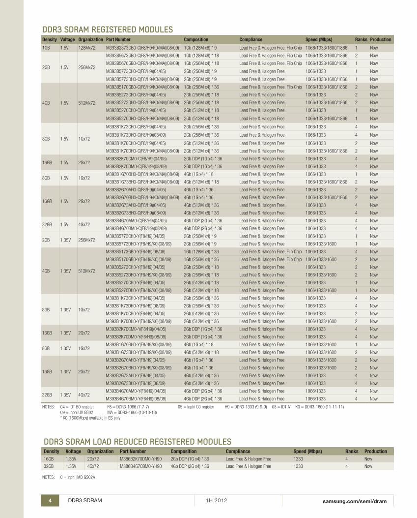
DDR3 SDRAM REGISTERED MODULESDensity Voltage Organization Part Number Composition Compliance Speed (Mbps) Ranks Production
1GB 1.5V 128Mx72 M393B2873GB0-C(F8/H9/K0/MA)(08/09) 1Gb (128M x8) * 9 Lead Free & Halogen Free, Flip Chip 1066/1333/1600/1866 1 Now
2GB 1.5V 256Mx72
M393B5673GB0-C(F8/H9/K0/MA)(08/09) 1Gb (128M x8) * 18 Lead Free & Halogen Free, Flip Chip 1066/1333/1600/1866 2 Now
M393B5670GB0-C(F8/H9/K0/MA)(08/09) 1Gb (256M x4) * 18 Lead Free & Halogen Free, Flip Chip 1066/1333/1600/1866 1 Now
M393B5773CH0-C(F8/H9)(04/05) 2Gb (256M x8) * 9 Lead Free & Halogen Free 1066/1333 1 Now
M393B5773DH0-C(F8/H9/K0/MA)(08/09) 2Gb (256M x8) * 9 Lead Free & Halogen Free 1066/1333/1600/1866 1 Now
4GB 1.5V 512Mx72
M393B5170GB0-C(F8/H9/K0/MA)(08/09) 1Gb (256M x4) * 36 Lead Free & Halogen Free, Flip Chip 1066/1333/1600/1866 2 Now
M393B5273CH0-C(F8/H9)(04/05) 2Gb (256M x8) * 18 Lead Free & Halogen Free 1066/1333 2 Now
M393B5273DH0-C(F8/H9/K0/MA)(08/09) 2Gb (256M x8) * 18 Lead Free & Halogen Free 1066/1333/1600/1866 2 Now
M393B5270CH0-C(F8/H9)(04/05) 2Gb (512M x4) * 18 Lead Free & Halogen Free 1066/1333 1 Now
M393B5270DH0-C(F8/H9/K0/MA)(08/09) 2Gb (512M x4) * 18 Lead Free & Halogen Free 1066/1333/1600/1866 1 Now
8GB 1.5V 1Gx72
M393B1K73CH0-C(F8/H9)(04/05) 2Gb (256M x8) * 36 Lead Free & Halogen Free 1066/1333 4 Now
M393B1K73DH0-C(F8/H9)(08/09) 2Gb (256M x8) * 36 Lead Free & Halogen Free 1066/1333 4 Now
M393B1K70CH0-C(F8/H9)(04/05) 2Gb (512M x4) * 36 Lead Free & Halogen Free 1066/1333 2 Now
M393B1K70DH0-C(F8/H9/K0/MA)(08/09) 2Gb (512M x4) * 36 Lead Free & Halogen Free 1066/1333/1600/1866 2 Now
16GB 1.5V 2Gx72M393B2K70CM0-C(F8/H9)(04/05) 2Gb DDP (1G x4) * 36 Lead Free & Halogen Free 1066/1333 4 Now
M393B2K70DM0-C(F8/H9)(08/09) 2Gb DDP (1G x4) * 36 Lead Free & Halogen Free 1066/1333 4 Now
8GB 1.5V 1Gx72M393B1G70BH0-C(F8/H9/K0/MA)(08/09) 4Gb (1G x4) * 18 Lead Free & Halogen Free 1066/1333 1 Now
M393B1G73BH0-C(F8/H9/K0/MA)(08/09) 4Gb (512M x8) * 18 Lead Free & Halogen Free 1066/1333/1600/1866 2 Now
16GB 1.5V 2Gx72
M393B2G70AH0-C(F8/H9)(04/05) 4Gb (1G x4) * 36 Lead Free & Halogen Free 1066/1333 2 Now
M393B2G70BH0-C(F8/H9/K0/MA)(08/09) 4Gb (1G x4) * 36 Lead Free & Halogen Free 1066/1333/1600/1866 2 Now
M393B2G73AH0-C(F8/H9)(04/05) 4Gb (512M x8) * 36 Lead Free & Halogen Free 1066/1333 4 Now
M393B2G73BH0-C(F8/H9)(08/09) 4Gb (512M x8) * 36 Lead Free & Halogen Free 1066/1333 4 Now
32GB 1.5V 4Gx72M393B4G70AM0-C(F8/H9)(04/05) 4Gb DDP (2G x4) * 36 Lead Free & Halogen Free 1066/1333 4 Now
M393B4G70BM0-C(F8/H9)(08/09) 4Gb DDP (2G x4) * 36 Lead Free & Halogen Free 1066/1333 4 Now
2GB 1.35V 256Mx72M393B5773CH0-Y(F8/H9)(04/05) 2Gb (256M x4) * 9 Lead Free & Halogen Free 1066/1333 1 Now
M393B5773DH0-Y(F8/H9/K0)(08/09) 2Gb (256M x4) * 9 Lead Free & Halogen Free 1066/1333/1600 1 Now
4GB 1.35V 512Mx72
M393B5173GB0-Y(F8/H9)(08/09) 1Gb (128M x8) * 36 Lead Free & Halogen Free, Flip Chip 1066/1333 4 Now
M393B5170GB0-Y(F8/H9/K0)(08/09) 1Gb (256M x4) * 36 Lead Free & Halogen Free, Flip Chip 1066/1333/1600 2 Now
M393B5273CH0-Y(F8/H9)(04/05) 2Gb (256M x8) * 18 Lead Free & Halogen Free 1066/1333 2 Now
M393B5273DH0-Y(F8/H9/K0)(08/09) 2Gb (256M x8) * 18 Lead Free & Halogen Free 1066/1333/1600 2 Now
M393B5270CH0-Y(F8/H9)(04/05) 2Gb (512M x4) * 18 Lead Free & Halogen Free 1066/1333 1 Now
M393B5270DH0-Y(F8/H9/K0)(08/09) 2Gb (512M x4) * 18 Lead Free & Halogen Free 1066/1333/1600 1 Now
8GB 1.35V 1Gx72
M393B1K73CH0-Y(F8/H9)(04/05) 2Gb (256M x8) * 36 Lead Free & Halogen Free 1066/1333 4 Now
M393B1K73DH0-Y(F8/H9)(08/09) 2Gb (256M x8) * 36 Lead Free & Halogen Free 1066/1333 4 Now
M393B1K70CH0-Y(F8/H9)(04/05) 2Gb (512M x4) * 36 Lead Free & Halogen Free 1066/1333 2 Now
M393B1K70DH0-Y(F8/H9/K0)(08/09) 2Gb (512M x4) * 36 Lead Free & Halogen Free 1066/1333/1600 2 Now
16GB 1.35V 2Gx72M393B2K70CM0-Y(F8/H9)(04/05) 2Gb DDP (1G x4) * 36 Lead Free & Halogen Free 1066/1333 4 Now
M393B2K70DM0-Y(F8/H9)(08/09) 2Gb DDP (1G x4) * 36 Lead Free & Halogen Free 1066/1333 4 Now
8GB 1.35V 1Gx72M393B1G70BH0-Y(F8/H9/K0)(08/09) 4Gb (1G x4) * 18 Lead Free & Halogen Free 1066/1333/1600 1 Now
M393B1G73BH0-Y(F8/H9/K0)(08/09) 4Gb (512M x8) * 18 Lead Free & Halogen Free 1066/1333/1600 2 Now
16GB 1.35V 2Gx72
M393B2G70AH0-Y(F8/H9)(04/05) 4Gb (1G x4) * 36 Lead Free & Halogen Free 1066/1333/1600 2 Now
M393B2G70BH0-Y(F8/H9/K0)(08/09) 4Gb (1G x4) * 36 Lead Free & Halogen Free 1066/1333/1600 2 Now
M393B2G73AH0-Y(F8/H9)(04/05) 4Gb (512M x8) * 36 Lead Free & Halogen Free 1066/1333 4 Now
M393B2G73BH0-Y(F8/H9)(08/09) 4Gb (512M x8) * 36 Lead Free & Halogen Free 1066/1333 4 Now
32GB 1.35V 4Gx72M393B4G70AM0-Y(F8/H9)(04/05) 4Gb DDP (2G x4) * 36 Lead Free & Halogen Free 1066/1333 4 Now
M393B4G70BM0-Y(F8/H9)(08/09) 4Gb DDP (2G x4) * 36 Lead Free & Halogen Free 1066/1333 4 Now
Notes: 04 = IDt B0 register F8 = DDR3-1066 (7-7-7) 05 = Inphi C0 register H9 = DDR3-1333 (9-9-9) 08 = IDt A1 K0 = DDR3-1600 (11-11-11) 09 = Inphi UV Gs02 MA = DDR3-1866 (13-13-13) * K0 (1600Mbps) available in es only
DDR3 SDRAM LOAD REDUCED REGISTERED MODULES Density Voltage Organization Part Number Composition Compliance Speed (Mbps) Ranks Production16GB 1.35V 2Gx72 M386B2K70DM0-YH90 2Gb DDP (1G x4) * 36 Lead Free & Halogen Free 1333 4 Now
32GB 1.35V 4Gx72 M386B4G70BM0-YH90 4Gb DDP (2G x4) * 36 Lead Free & Halogen Free 1333 4 Now
Notes: 0 = Inphi iMB Gs02A
samsung.com/semi/dram
samsung.com/semi/dram 5
DR
AM
1H 2012 DDR3 SDRAM
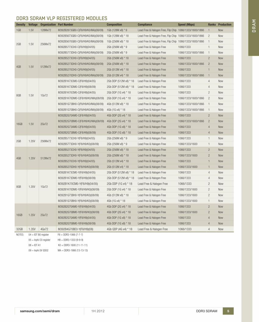
DDR3 SDRAM VLP REGISTERED MODULESDensity Voltage Organization Part Number Composition Compliance Speed (Mbps) Ranks Production
1GB 1.5V 128Mx72 M392B2873GB0-C(F8/H9/K0/MA)(08/09) 1Gb (128M x8) * 9 Lead Free & Halogen Free, Flip Chip 1066/1333/1600/1866 1 Now
2GB 1.5V 256Mx72
M392B5673GB0-C(F8/H9/K0/MA)(08/09) 1Gb (128M x8) * 18 Lead Free & Halogen Free, Flip Chip 1066/1333/1600/1866 2 Now
M392B5670GB0-C(F8/H9/K0/MA)(08/09) 1Gb (256M x8) * 18 Lead Free & Halogen Free, Flip Chip 1066/1333/1600/1866 1 Now
M392B5773CH0-C(F8/H9)(04/05) 2Gb (256M x8) * 9 Lead Free & Halogen Free 1066/1333 1 Now
M392B5773DH0-C(F8/H9/K0/MA)(08/09) 2Gb (256M x8) * 9 Lead Free & Halogen Free 1066/1333/1600/1866 1 Now
4GB 1.5V 512Mx72
M392B5273CH0-C(F8/H9)(04/05) 2Gb (256M x8) * 18 Lead Free & Halogen Free 1066/1333 2 Now
M392B5273DH0-C(F8/H9/K0/MA)(08/09) 2Gb (256M x8) * 18 Lead Free & Halogen Free 1066/1333/1600/1866 2 Now
M392B5270CH0-C(F8/H9)(04/05) 2Gb (512M x4) * 18 Lead Free & Halogen Free 1066/1333 1 Now
M392B5270DH0-C(F8/H9/K0/MA)(08/09) 2Gb (512M x4) * 18 Lead Free & Halogen Free 1066/1333/1600/1866 1 Now
8GB 1.5V 1Gx72
M392B1K73CM0-C(F8/H9)(04/05) 2Gb DDP (512M x8) * 18 Lead Free & Halogen Free 1066/1333 4 Now
M392B1K73DM0-C(F8/H9)(08/09) 2Gb DDP (512M x8) * 18 Lead Free & Halogen Free 1066/1333 4 Now
M392B1K70CM0-C(F8/H9)(04/05) 2Gb DDP (1G x4) * 18 Lead Free & Halogen Free 1066/1333 2 Now
M392B1K70DM0-C(F8/H9/K0/MA)(08/09) 2Gb DDP (1G x4) * 18 Lead Free & Halogen Free 1066/1333/1600/1866 2 Now
M392B1G73BH0-C(F8/H9/K0/MA)(08/09) 4Gb (512M x8) * 18 Lead Free & Halogen Free 1066/1333/1600/1866 1 Now
M392B1G70BH0-C(F8/H9/K0/MA)(08/09) 4Gb (1G x4) * 18 Lead Free & Halogen Free 1066/1333/1600/1866 1 Now
16GB 1.5V 2Gx72
M392B2G70AM0-C(F8/H9)(04/05) 4Gb DDP (2G x4) * 18 Lead Free & Halogen Free 1066/1333 2 Now
M392B2G70BM0-C(F8/H9/K0/MA)(08/09) 4Gb DDP (2G x4) * 18 Lead Free & Halogen Free 1066/1333/1600/1866 2 Now
M392B2G73AM0-C(F8/H9)(04/05) 4Gb DDP (1G x8) * 18 Lead Free & Halogen Free 1066/1333 4 Now
M392B2G73BM0-C(F8/H9)(08/09) 4Gb DDP (1G x8) * 18 Lead Free & Halogen Free 1066/1333 4 Now
2GB 1.35V 256Mx72M392B5773CH0-Y(F8/H9)(04/05) 2Gb (256M x8) * 9 Lead Free & Halogen Free 1066/1333 1 Now
M392B5773DH0-Y(F8/H9/K0)(08/09) 2Gb (256M x8) * 9 Lead Free & Halogen Free 1066/1333/1600 1 Now
4GB 1.35V 512Mx72
M392B5273CH0-Y(F8/H9)(04/05) 2Gb (256M x8) * 18 Lead Free & Halogen Free 1066/1333 2 Now
M392B5273DH0-Y(F8/H9/K0)(08/09) 2Gb (256M x8) * 18 Lead Free & Halogen Free 1066/1333/1600 2 Now
M392B5270CH0-Y(F8/H9)(04/05) 2Gb (512M x4) * 18 Lead Free & Halogen Free 1066/1333 1 Now
M392B5270DH0-Y(F8/H9/K0)(08/09) 2Gb (512M x4) * 18 Lead Free & Halogen Free 1066/1333/1600 1 Now
8GB 1.35V 1Gx72
M392B1K73CM0-Y(F8/H9)(04/05) 2Gb DDP (512M x8) * 18 Lead Free & Halogen Free 1066/1333 4 Now
M392B1K73DM0-Y(F8/H9)(08/09) 2Gb DDP (512M x8) * 18 Lead Free & Halogen Free 1066/1333 4 Now
M392B1K70CM0-Y(F8/H9)(04/05) 2Gb DDP (1G x4) * 18 Lead Free & Halogen Free 1066/1333 2 Now
M392B1K70DM0-Y(F8/H9/K0)(08/09) 2Gb DDP (1G x4) * 18 Lead Free & Halogen Free 1066/1333/1600 2 Now
M392B1G73BH0-Y(F8/H9/K0)(08/09) 4Gb (512M x8) * 18 Lead Free & Halogen Free 1066/1333/1600 2 Now
M392B1G70BH0-Y(F8/H9/K0)(08/09) 4Gb (1G x4) * 18 Lead Free & Halogen Free 1066/1333/1600 1 Now
16GB 1.35V 2Gx72
M392B2G70AM0-Y(F8/H9)(04/05) 4Gb DDP (2G x4) * 18 Lead Free & Halogen Free 1066/1333 2 Now
M392B2G70BM0-Y(F8/H9/K0)(08/09) 4Gb DDP (2G x4) * 18 Lead Free & Halogen Free 1066/1333/1600 2 Now
M392B2G70AM0-Y(F8/H9)(04/05) 4Gb DDP (1G x8) * 18 Lead Free & Halogen Free 1066/1333 4 Now
M392B2G70BM0-Y(F8/H9)(08/09) 4Gb DDP (1G x8) * 18 Lead Free & Halogen Free 1066/1333 4 Now
32GB 1.35V 4Gx72 M392B4G70Be0-Y(F8/H9)(08) 4Gb QDP (4G x4) * 18 Lead Free & Halogen Free 1066/1333 4 Now
Notes: 04 = IDt B0 register F8 = DDR3-1066 (7-7-7)
05 = Inphi C0 register H9 = DDR3-1333 (9-9-9)
08 = IDt A1 K0 = DDR3-1600 (11-11-11)
09 = Inphi UV Gs02 MA = DDR3-1866 (13-13-13)
samsung.com/semi/dram6 1H 2012DDR3 SDRAM
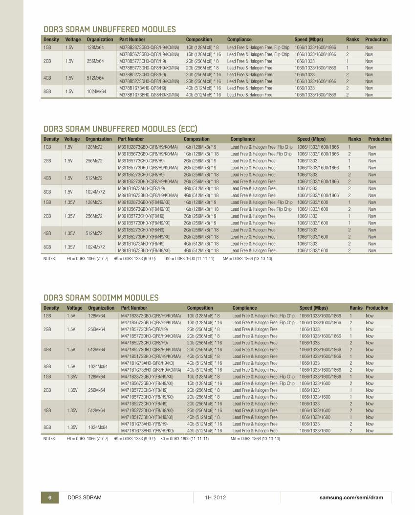
DDR3 SDRAM SODIMM MODULESDensity Voltage Organization Part Number Composition Compliance Speed (Mbps) Ranks Production
1GB 1.5V 128Mx64 M471B2873GB0-C(F8/H9/K0/MA) 1Gb (128M x8) * 8 Lead Free & Halogen Free, Flip Chip 1066/1333/1600/1866 1 Now
2GB 1.5V 256Mx64M471B5673GB0-C(F8/H9/K0/MA) 1Gb (128M x8) * 16 Lead Free & Halogen Free, Flip Chip 1066/1333/1600/1866 2 NowM471B5773CHs-C(F8/H9) 2Gb (256M x8) * 8 Lead Free & Halogen Free 1066/1333 1 NowM471B5773DH0-C(F8/H9/K0/MA) 2Gb (256M x8) * 8 Lead Free & Halogen Free 1066/1333/1600/1866 1 Now
4GB 1.5V 512Mx64M471B5273CH0-C(F8/H9) 2Gb (256M x8) * 16 Lead Free & Halogen Free 1066/1333 2 NowM471B5273DH0-C(F8/H9/K0/MA) 2Gb (256M x8) * 16 Lead Free & Halogen Free 1066/1333/1600/1866 2 NowM471B5173BH0-C(F8/H9/K0/MA) 4Gb (512M x8) * 8 Lead Free & Halogen Free 1066/1333/1600/1866 1 Now
8GB 1.5V 1024Mx64M471B1G73AH0-C(F8/H9/K0) 4Gb (512M x8) * 16 Lead Free & Halogen Free 1066/1333 2 NowM471B1G73BH0-C(F8/H9/K0/MA) 4Gb (512M x8) * 16 Lead Free & Halogen Free 1066/1333/1600/1866 2 Now
1GB 1.35V 128Mx64 M471B2873GB0-Y(F8/H9/K0) 1Gb (128M x8) * 8 Lead Free & Halogen Free, Flip Chip 1066/1333/1600/1866 1 Now
2GB 1.35V 256Mx64M471B5673GB0-Y(F8/H9/K0) 1Gb (128M x8) * 16 Lead Free & Halogen Free, Flip Chip 1066/1333/1600 2 NowM471B5773CHs-Y(F8/H9) 2Gb (256M x8) * 8 Lead Free & Halogen Free 1066/1333 1 NowM471B5773DH0-Y(F8/H9/K0) 2Gb (256M x8) * 8 Lead Free & Halogen Free 1066/1333/1600 1 Now
4GB 1.35V 512Mx64M471B5273CH0-Y(F8/H9) 2Gb (256M x8) * 16 Lead Free & Halogen Free 1066/1333 2 NowM471B5273DH0-Y(F8/H9/K0) 2Gb (256M x8) * 16 Lead Free & Halogen Free 1066/1333/1600 2 NowM471B5173BH0-Y(F8/H9/K0) 4Gb (512M x8) * 8 Lead Free & Halogen Free 1066/1333/1600 1 Now
8GB 1.35V 1024Mx64M471B1G73AH0-Y(F8/H9) 4Gb (512M x8) * 16 Lead Free & Halogen Free 1066/1333 2 NowM471B1G73BH0-Y(F8/H9/K0) 4Gb (512M x8) * 16 Lead Free & Halogen Free 1066/1333/1600 2 Now
Notes: F8 = DDR3-1066 (7-7-7) H9 = DDR3-1333 (9-9-9) K0 = DDR3-1600 (11-11-11) MA = DDR3-1866 (13-13-13)
DDR3 SDRAM UNBUFFERED MODULES Density Voltage Organization Part Number Composition Compliance Speed (Mbps) Ranks Production
1GB 1.5V 128Mx64 M378B2873GB0-C(F8/H9/K0/MA) 1Gb (128M x8) * 8 Lead Free & Halogen Free, Flip Chip 1066/1333/1600/1866 1 Now
2GB 1.5V 256Mx64M378B5673GB0-C(F8/H9/K0/MA) 1Gb (128M x8) * 16 Lead Free & Halogen Free, Flip Chip 1066/1333/1600/1866 2 NowM378B5773CH0-C(F8/H9) 2Gb (256M x8) * 8 Lead Free & Halogen Free 1066/1333 1 NowM378B5773DH0-C(F8/H9/K0/MA) 2Gb (256M x8) * 8 Lead Free & Halogen Free 1066/1333/1600/1866 1 Now
4GB 1.5V 512Mx64M378B5273CH0-C(F8/H9) 2Gb (256M x8) * 16 Lead Free & Halogen Free 1066/1333 2 NowM378B5273DH0-C(F8/H9/K0/MA) 2Gb (256M x8) * 16 Lead Free & Halogen Free 1066/1333/1600/1866 2 Now
8GB 1.5V 1024Mx64M378B1G73AH0-C(F8/H9) 4Gb (512M x8) * 16 Lead Free & Halogen Free 1066/1333 2 NowM378B1G73BH0-C(F8/H9/K0/MA) 4Gb (512M x8) * 16 Lead Free & Halogen Free 1066/1333/1600/1866 2 Now
DDR3 SDRAM UNBUFFERED MODULES (ECC)Density Voltage Organization Part Number Composition Compliance Speed (Mbps) Ranks Production
1GB 1.5V 128Mx72 M391B2873GB0-C(F8/H9/K0/MA) 1Gb (128M x8) * 9 Lead Free & Halogen Free, Flip Chip 1066/1333/1600/1866 1 Now
2GB 1.5V 256Mx72
M391B5673GB0-C(F8/H9/K0/MA) 1Gb (128M x8) * 18 Lead Free & Halogen Free,Flip Chip 1066/1333/1600/1866 2 Now
M391B5773CH0-C(F8/H9) 2Gb (256M x8) * 9 Lead Free & Halogen Free 1066/1333 1 Now
M391B5773DH0-C(F8/H9/K0/MA) 2Gb (256M x8) * 9 Lead Free & Halogen Free 1066/1333/1600/1866 1 Now
4GB 1.5V 512Mx72M391B5273CH0-C(F8/H9) 2Gb (256M x8) * 18 Lead Free & Halogen Free 1066/1333 2 Now
M391B5273DH0-C(F8/H9/K0/MA) 2Gb (256M x8) * 18 Lead Free & Halogen Free 1066/1333/1600/1866 2 Now
8GB 1.5V 1024Mx72M391B1G73AH0-C(F8/H9) 4Gb (512M x8) * 18 Lead Free & Halogen Free 1066/1333 2 Now
M391B1G73BH0-C(F8/H9/K0/MA) 4Gb (512M x8) * 18 Lead Free & Halogen Free 1066/1333/1600/1866 2 Now
1GB 1.35V 128Mx72 M391B2873GB0-Y(F8/H9/K0) 1Gb (128M x8) * 9 Lead Free & Halogen Free, Flip Chip 1066/1333/1600 1 Now
2GB 1.35V 256Mx72
M391B5673GB0-Y(F8/H9/K0) 1Gb (128M x8) * 18 Lead Free & Halogen Free,Flip Chip 1066/1333/1600 2 Now
M391B5773CH0-Y(F8/H9) 2Gb (256M x8) * 9 Lead Free & Halogen Free 1066/1333 1 Now
M391B5773DH0-Y(F8/H9/K0) 2Gb (256M x8) * 9 Lead Free & Halogen Free 1066/1333/1600 1 Now
4GB 1.35V 512Mx72M391B5273CH0-Y(F8/H9) 2Gb (256M x8) * 18 Lead Free & Halogen Free 1066/1333 2 Now
M391B5273DH0-Y(F8/H9/K0) 2Gb (256M x8) * 18 Lead Free & Halogen Free 1066/1333/1600 2 Now
8GB 1.35V 1024Mx72M391B1G73AH0-Y(F8/H9) 4Gb (512M x8) * 18 Lead Free & Halogen Free 1066/1333 2 NowM391B1G73BH0-Y(F8/H9/K0) 4Gb (512M x8) * 18 Lead Free & Halogen Free 1066/1333/1600 2 Now
Notes: F8 = DDR3-1066 (7-7-7) H9 = DDR3-1333 (9-9-9) K0 = DDR3-1600 (11-11-11) MA = DDR3-1866 (13-13-13)
samsung.com/semi/dram 7
DR
AM
1H 2012 DDR3 & DDR2 SDRAM
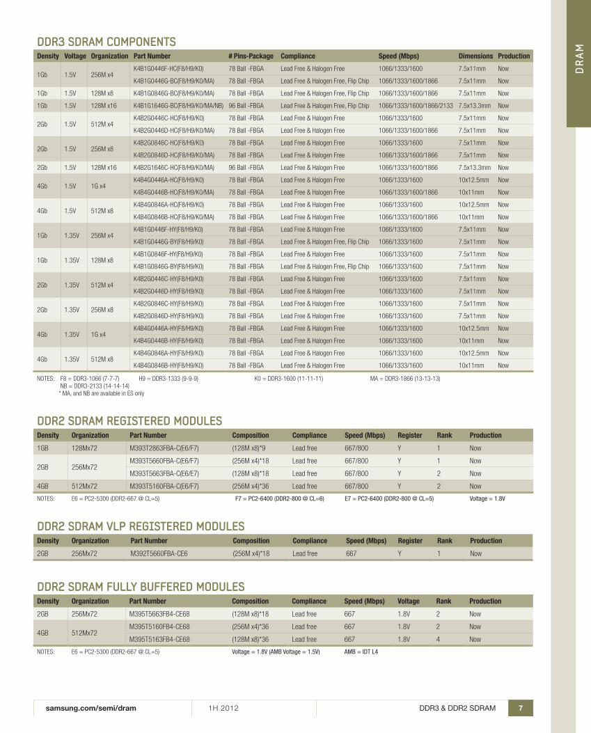
DDR3 SDRAM COMPONENTSDensity Voltage Organization Part Number # Pins-Package Compliance Speed (Mbps) Dimensions Production
1Gb 1.5V 256M x4K4B1G0446F-HC(F8/H9/K0) 78 Ball -FBGA Lead Free & Halogen Free 1066/1333/1600 7.5x11mm Now
K4B1G0446G-BC(F8/H9/K0/MA) 78 Ball -FBGA Lead Free & Halogen Free, Flip Chip 1066/1333/1600/1866 7.5x11mm Now
1Gb 1.5V 128M x8 K4B1G0846G-BC(F8/H9/K0/MA) 78 Ball -FBGA Lead Free & Halogen Free, Flip Chip 1066/1333/1600/1866 7.5x11mm Now
1Gb 1.5V 128M x16 K4B1G1646G-BC(F8/H9/K0/MA/NB) 96 Ball -FBGA Lead Free & Halogen Free, Flip Chip 1066/1333/1600/1866/2133 7.5x13.3mm Now
2Gb 1.5V 512M x4K4B2G0446C-HC(F8/H9/K0) 78 Ball -FBGA Lead Free & Halogen Free 1066/1333/1600 7.5x11mm Now
K4B2G0446D-HC(F8/H9/K0/MA) 78 Ball -FBGA Lead Free & Halogen Free 1066/1333/1600/1866 7.5x11mm Now
2Gb 1.5V 256M x8K4B2G0846C-HC(F8/H9/K0) 78 Ball -FBGA Lead Free & Halogen Free 1066/1333/1600 7.5x11mm Now
K4B2G0846D-HC(F8/H9/K0/MA) 78 Ball -FBGA Lead Free & Halogen Free 1066/1333/1600/1866 7.5x11mm Now
2Gb 1.5V 128M x16 K4B2G1646C-HC(F8/H9/K0/MA) 96 Ball -FBGA Lead Free & Halogen Free 1066/1333/1600/1866 7.5x13.3mm Now
4Gb 1.5V 1G x4K4B4G0446A-HC(F8/H9/K0) 78 Ball -FBGA Lead Free & Halogen Free 1066/1333/1600 10x12.5mm Now
K4B4G0446B-HC(F8/H9/K0/MA) 78 Ball -FBGA Lead Free & Halogen Free 1066/1333/1600/1866 10x11mm Now
4Gb 1.5V 512M x8K4B4G0846A-HC(F8/H9/K0) 78 Ball -FBGA Lead Free & Halogen Free 1066/1333/1600 10x12.5mm Now
K4B4G0846B-HC(F8/H9/K0/MA) 78 Ball -FBGA Lead Free & Halogen Free 1066/1333/1600/1866 10x11mm Now
1Gb 1.35V 256M x4K4B1G0446F-HY(F8/H9/K0) 78 Ball -FBGA Lead Free & Halogen Free 1066/1333/1600 7.5x11mm Now
K4B1G0446G-BY(F8/H9/K0) 78 Ball -FBGA Lead Free & Halogen Free, Flip Chip 1066/1333/1600 7.5x11mm Now
1Gb 1.35V 128M x8K4B1G0846F-HY(F8/H9/K0) 78 Ball -FBGA Lead Free & Halogen Free 1066/1333/1600 7.5x11mm Now
K4B1G0846G-BY(F8/H9/K0) 78 Ball -FBGA Lead Free & Halogen Free, Flip Chip 1066/1333/1600 7.5x11mm Now
2Gb 1.35V 512M x4K4B2G0446C-HY(F8/H9/K0) 78 Ball -FBGA Lead Free & Halogen Free 1066/1333/1600 7.5x11mm Now
K4B2G0446D-HY(F8/H9/K0) 78 Ball -FBGA Lead Free & Halogen Free 1066/1333/1600 7.5x11mm Now
2Gb 1.35V 256M x8K4B2G0846C-HY(F8/H9/K0) 78 Ball -FBGA Lead Free & Halogen Free 1066/1333/1600 7.5x11mm Now
K4B2G0846D-HY(F8/H9/K0) 78 Ball -FBGA Lead Free & Halogen Free 1066/1333/1600 7.5x11mm Now
4Gb 1.35V 1G x4K4B4G0446A-HY(F8/H9/K0) 78 Ball -FBGA Lead Free & Halogen Free 1066/1333/1600 10x12.5mm Now
K4B4G0446B-HY(F8/H9/K0) 78 Ball -FBGA Lead Free & Halogen Free 1066/1333/1600 10x11mm Now
4Gb 1.35V 512M x8K4B4G0846A-HY(F8/H9/K0) 78 Ball -FBGA Lead Free & Halogen Free 1066/1333/1600 10x12.5mm Now
K4B4G0846B-HY(F8/H9/K0) 78 Ball -FBGA Lead Free & Halogen Free 1066/1333/1600 10x11mm Now
DDR2 SDRAM REGISTERED MODULESDensity Organization Part Number Composition Compliance Speed (Mbps) Register Rank Production
1GB 128Mx72 M393t2863FBA-C(e6/F7) (128M x8)*9 Lead free 667/800 Y 1 Now
2GB 256Mx72M393t5660FBA-C(e6/F7) (256M x4)*18 Lead free 667/800 Y 1 Now
M393t5663FBA-C(e6/e7) (128M x8)*18 Lead free 667/800 Y 2 Now
4GB 512Mx72 M393t5160FBA-C(e6/F7) (256M x4)*36 Lead free 667/800 Y 2 Now
Notes: e6 = PC2-5300 (DDR2-667 @ CL=5) F7 = PC2-6400 (DDR2-800 @ CL=6) E7 = PC2-6400 (DDR2-800 @ CL=5) Voltage = 1.8V
DDR2 SDRAM VLP REGISTERED MODULESDensity Organization Part Number Composition Compliance Speed (Mbps) Register Rank Production
2GB 256Mx72 M392t5660FBA-Ce6 (256M x4)*18 Lead free 667 Y 1 Now
DDR2 SDRAM FULLY BUFFERED MODULESDensity Organization Part Number Composition Compliance Speed (Mbps) Voltage Rank Production
2GB 256Mx72 M395t5663FB4-Ce68 (128M x8)*18 Lead free 667 1.8V 2 Now
4GB 512Mx72M395t5160FB4-Ce68 (256M x4)*36 Lead free 667 1.8V 2 Now
M395t5163FB4-Ce68 (128M x8)*36 Lead free 667 1.8V 4 Now
Notes: e6 = PC2-5300 (DDR2-667 @ CL=5) Voltage = 1.8V (AMB Voltage = 1.5V) AMB = IDT L4
Notes: F8 = DDR3-1066 (7-7-7) H9 = DDR3-1333 (9-9-9) K0 = DDR3-1600 (11-11-11) MA = DDR3-1866 (13-13-13) NB = DDR3-2133 (14-14-14) * MA, and NB are available in es only
samsung.com/semi/dram8 1H 2012DDR2, DDR & SDRAM COMPONENTS
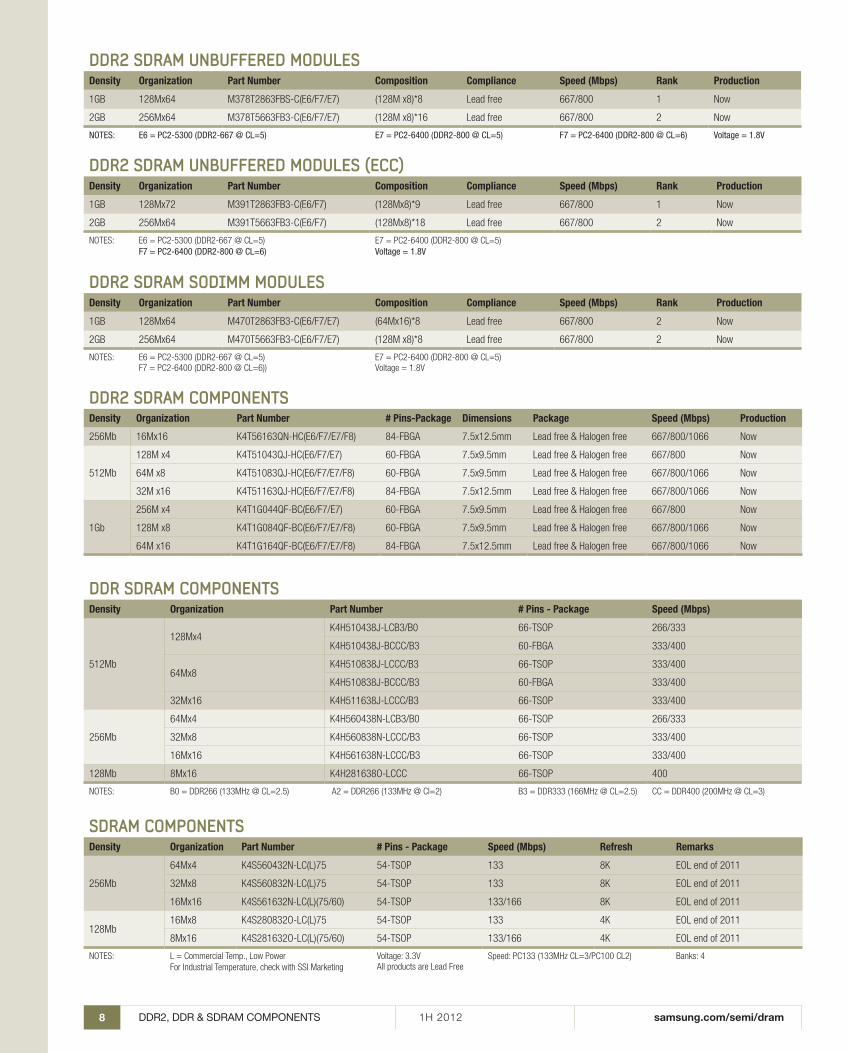
SDRAM COMPONENTSDensity Organization Part Number # Pins - Package Speed (Mbps) Refresh Remarks
256Mb
64Mx4 K4s560432N-LC(L)75 54-tsoP 133 8K eoL end of 2011
32Mx8 K4s560832N-LC(L)75 54-tsoP 133 8K eoL end of 2011
16Mx16 K4s561632N-LC(L)(75/60) 54-tsoP 133/166 8K eoL end of 2011
128Mb16Mx8 K4s280832o-LC(L)75 54-tsoP 133 4K eoL end of 2011
8Mx16 K4s281632o-LC(L)(75/60) 54-tsoP 133/166 4K eoL end of 2011
Notes: L = Commercial temp., Low PowerFor Industrial temperature, check with ssI Marketing
Voltage: 3.3VAll products are Lead Free
speed: PC133 (133MHz CL=3/PC100 CL2) Banks: 4
DDR SDRAM COMPONENTSDensity Organization Part Number # Pins - Package Speed (Mbps)
512Mb
128Mx4K4H510438J-LCB3/B0 66-tsoP 266/333
K4H510438J-BCCC/B3 60-FBGA 333/400
64Mx8K4H510838J-LCCC/B3 66-tsoP 333/400
K4H510838J-BCCC/B3 60-FBGA 333/400
32Mx16 K4H511638J-LCCC/B3 66-tsoP 333/400
256Mb
64Mx4 K4H560438N-LCB3/B0 66-tsoP 266/333
32Mx8 K4H560838N-LCCC/B3 66-tsoP 333/400
16Mx16 K4H561638N-LCCC/B3 66-tsoP 333/400
128Mb 8Mx16 K4H281638o-LCCC 66-tsoP 400
Notes: B0 = DDR266 (133MHz @ CL=2.5) A2 = DDR266 (133MHz @ Cl=2) B3 = DDR333 (166MHz @ CL=2.5) CC = DDR400 (200MHz @ CL=3)
DDR2 SDRAM UNBUFFERED MODULES (ECC)Density Organization Part Number Composition Compliance Speed (Mbps) Rank Production
1GB 128Mx72 M391t2863FB3-C(e6/F7) (128Mx8)*9 Lead free 667/800 1 Now
2GB 256Mx64 M391t5663FB3-C(e6/F7) (128Mx8)*18 Lead free 667/800 2 Now
Notes: e6 = PC2-5300 (DDR2-667 @ CL=5)F7 = PC2-6400 (DDR2-800 @ CL=6)
e7 = PC2-6400 (DDR2-800 @ CL=5)Voltage = 1.8V
DDR2 SDRAM SODIMM MODULESDensity Organization Part Number Composition Compliance Speed (Mbps) Rank Production
1GB 128Mx64 M470t2863FB3-C(e6/F7/e7) (64Mx16)*8 Lead free 667/800 2 Now
2GB 256Mx64 M470t5663FB3-C(e6/F7/e7) (128M x8)*8 Lead free 667/800 2 Now
Notes: e6 = PC2-5300 (DDR2-667 @ CL=5)F7 = PC2-6400 (DDR2-800 @ CL=6))
e7 = PC2-6400 (DDR2-800 @ CL=5)Voltage = 1.8V
DDR2 SDRAM COMPONENTSDensity Organization Part Number # Pins-Package Dimensions Package Speed (Mbps) Production
256Mb 16Mx16 K4t56163QN-HC(e6/F7/e7/F8) 84-FBGA 7.5x12.5mm Lead free & Halogen free 667/800/1066 Now
512Mb
128M x4 K4t51043QJ-HC(e6/F7/e7) 60-FBGA 7.5x9.5mm Lead free & Halogen free 667/800 Now
64M x8 K4t51083QJ-HC(e6/F7/e7/F8) 60-FBGA 7.5x9.5mm Lead free & Halogen free 667/800/1066 Now
32M x16 K4t51163QJ-HC(e6/F7/e7/F8) 84-FBGA 7.5x12.5mm Lead free & Halogen free 667/800/1066 Now
1Gb
256M x4 K4t1G044QF-BC(e6/F7/e7) 60-FBGA 7.5x9.5mm Lead free & Halogen free 667/800 Now
128M x8 K4t1G084QF-BC(e6/F7/e7/F8) 60-FBGA 7.5x9.5mm Lead free & Halogen free 667/800/1066 Now
64M x16 K4t1G164QF-BC(e6/F7/e7/F8) 84-FBGA 7.5x12.5mm Lead free & Halogen free 667/800/1066 Now
DDR2 SDRAM UNBUFFERED MODULES Density Organization Part Number Composition Compliance Speed (Mbps) Rank Production
1GB 128Mx64 M378t2863FBs-C(e6/F7/e7) (128M x8)*8 Lead free 667/800 1 Now
2GB 256Mx64 M378t5663FB3-C(e6/F7/e7) (128M x8)*16 Lead free 667/800 2 Now
NoTEs: E6 = PC2-5300 (DDR2-667 @ CL=5) E7 = PC2-6400 (DDR2-800 @ CL=5) F7 = PC2-6400 (DDR2-800 @ CL=6) Voltage = 1.8V
samsung.com/semi/dram 9
DR
AM
1H 2012 Mobile & Graphics DRAM Components
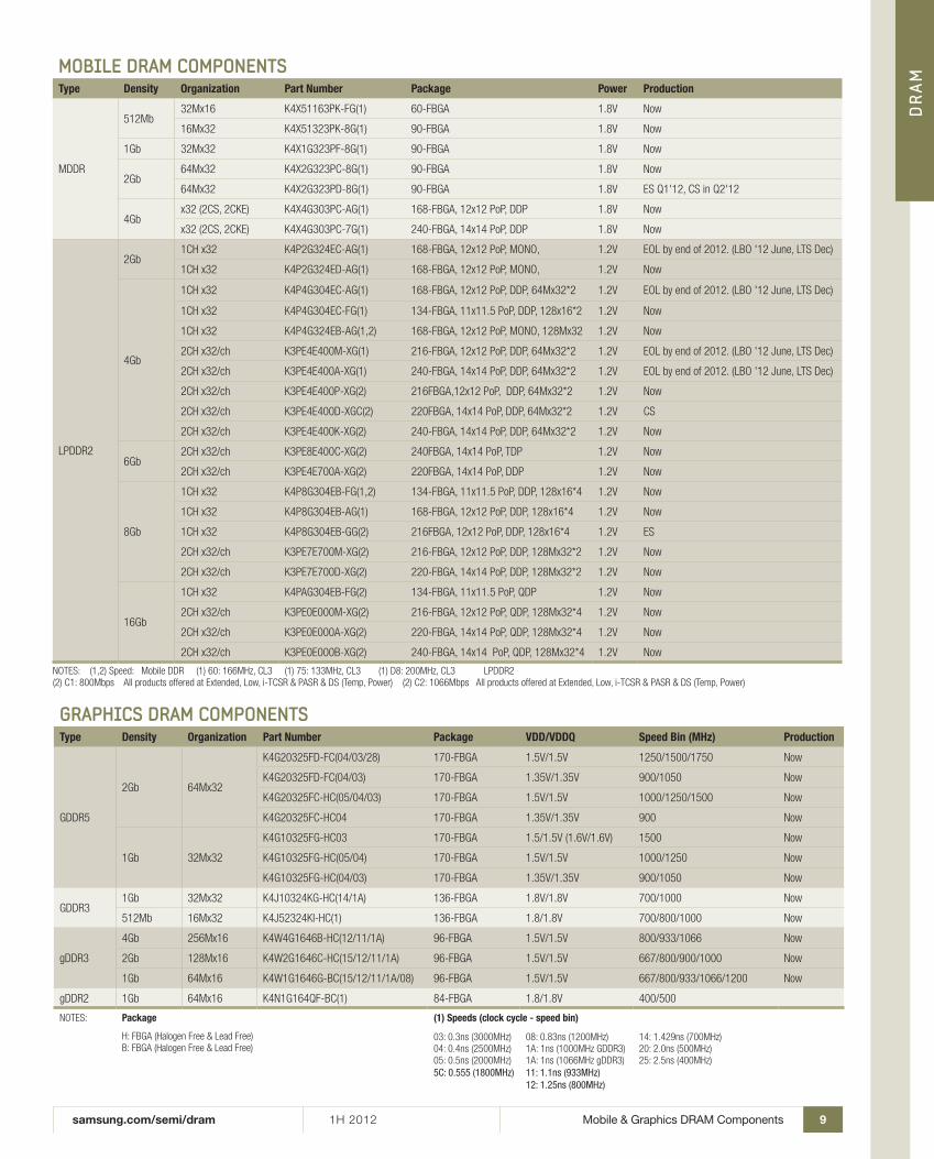
GRAPHICS DRAM COMPONENTSType Density Organization Part Number Package VDD/VDDQ Speed Bin (MHz) Production
GDDR5
2Gb 64Mx32
K4G20325FD-FC(04/03/28) 170-FBGA 1.5V/1.5V 1250/1500/1750 Now
K4G20325FD-FC(04/03) 170-FBGA 1.35V/1.35V 900/1050 Now
K4G20325FC-HC(05/04/03) 170-FBGA 1.5V/1.5V 1000/1250/1500 Now
K4G20325FC-HC04 170-FBGA 1.35V/1.35V 900 Now
1Gb 32Mx32
K4G10325FG-HC03 170-FBGA 1.5/1.5V (1.6V/1.6V) 1500 Now
K4G10325FG-HC(05/04) 170-FBGA 1.5V/1.5V 1000/1250 Now
K4G10325FG-HC(04/03) 170-FBGA 1.35V/1.35V 900/1050 Now
GDDR31Gb 32Mx32 K4J10324KG-HC(14/1A) 136-FBGA 1.8V/1.8V 700/1000 Now
512Mb 16Mx32 K4J52324KI-HC(1) 136-FBGA 1.8/1.8V 700/800/1000 Now
gDDR3
4Gb 256Mx16 K4W4G1646B-HC(12/11/1A) 96-FBGA 1.5V/1.5V 800/933/1066 Now
2Gb 128Mx16 K4W2G1646C-HC(15/12/11/1A) 96-FBGA 1.5V/1.5V 667/800/900/1000 Now
1Gb 64Mx16 K4W1G1646G-BC(15/12/11/1A/08) 96-FBGA 1.5V/1.5V 667/800/933/1066/1200 Now
gDDR2 1Gb 64Mx16 K4N1G164QF-BC(1) 84-FBGA 1.8/1.8V 400/500
Notes: Package
H: FBGA (Halogen Free & Lead Free) B: FBGA (Halogen Free & Lead Free)
(1) Speeds (clock cycle - speed bin)
03: 0.3ns (3000MHz)04: 0.4ns (2500MHz)05: 0.5ns (2000MHz)5C: 0.555 (1800MHz)
08: 0.83ns (1200MHz) 1A: 1ns (1000MHz GDDR3) 1A: 1ns (1066MHz gDDR3)11: 1.1ns (933MHz) 12: 1.25ns (800MHz)
14: 1.429ns (700MHz)20: 2.0ns (500MHz)25: 2.5ns (400MHz)
MOBILE DRAM COMPONENTSType Density Organization Part Number Package Power Production
MDDR
512Mb32Mx16 K4X51163PK-FG(1) 60-FBGA 1.8V Now
16Mx32 K4X51323PK-8G(1) 90-FBGA 1.8V Now
1Gb 32Mx32 K4X1G323PF-8G(1) 90-FBGA 1.8V Now
2Gb64Mx32 K4X2G323PC-8G(1) 90-FBGA 1.8V Now
64Mx32 K4X2G323PD-8G(1) 90-FBGA 1.8V es Q1'12, Cs in Q2'12
4Gbx32 (2Cs, 2CKe) K4X4G303PC-AG(1) 168-FBGA, 12x12 PoP, DDP 1.8V Now
x32 (2Cs, 2CKe) K4X4G303PC-7G(1) 240-FBGA, 14x14 PoP, DDP 1.8V Now
LPDDR2
2Gb1CH x32 K4P2G324eC-AG(1) 168-FBGA, 12x12 PoP, MoNo, 1.2V eoL by end of 2012. (LBo '12 June, Lts Dec)
1CH x32 K4P2G324eD-AG(1) 168-FBGA, 12x12 PoP, MoNo, 1.2V Now
4Gb
1CH x32 K4P4G304eC-AG(1) 168-FBGA, 12x12 PoP, DDP, 64Mx32*2 1.2V eoL by end of 2012. (LBo '12 June, Lts Dec)
1CH x32 K4P4G304eC-FG(1) 134-FBGA, 11x11.5 PoP, DDP, 128x16*2 1.2V Now
1CH x32 K4P4G324eB-AG(1,2) 168-FBGA, 12x12 PoP, MoNo, 128Mx32 1.2V Now
2CH x32/ch K3Pe4e400M-XG(1) 216-FBGA, 12x12 PoP, DDP, 64Mx32*2 1.2V eoL by end of 2012. (LBo '12 June, Lts Dec)
2CH x32/ch K3Pe4e400A-XG(1) 240-FBGA, 14x14 PoP, DDP, 64Mx32*2 1.2V eoL by end of 2012. (LBo '12 June, Lts Dec)
2CH x32/ch K3Pe4e400P-XG(2) 216FBGA,12x12 PoP, DDP, 64Mx32*2 1.2V Now
2CH x32/ch K3Pe4e400D-XGC(2) 220FBGA, 14x14 PoP, DDP, 64Mx32*2 1.2V Cs
2CH x32/ch K3Pe4e400K-XG(2) 240-FBGA, 14x14 PoP, DDP, 64Mx32*2 1.2V Now
6Gb2CH x32/ch K3Pe8e400C-XG(2) 240FBGA, 14x14 PoP, tDP 1.2V Now
2CH x32/ch K3Pe4e700A-XG(2) 220FBGA, 14x14 PoP, DDP 1.2V Now
8Gb
1CH x32 K4P8G304eB-FG(1,2) 134-FBGA, 11x11.5 PoP, DDP, 128x16*4 1.2V Now
1CH x32 K4P8G304eB-AG(1) 168-FBGA, 12x12 PoP, DDP, 128x16*4 1.2V Now
1CH x32 K4P8G304eB-GG(2) 216FBGA, 12x12 PoP, DDP, 128x16*4 1.2V es
2CH x32/ch K3Pe7e700M-XG(2) 216-FBGA, 12x12 PoP, DDP, 128Mx32*2 1.2V Now
2CH x32/ch K3Pe7e700D-XG(2) 220-FBGA, 14x14 PoP, DDP, 128Mx32*2 1.2V Now
16Gb
1CH x32 K4PAG304eB-FG(2) 134-FBGA, 11x11.5 PoP, QDP 1.2V Now
2CH x32/ch K3Pe0e000M-XG(2) 216-FBGA, 12x12 PoP, QDP, 128Mx32*4 1.2V Now
2CH x32/ch K3Pe0e000A-XG(2) 220-FBGA, 14x14 PoP, QDP, 128Mx32*4 1.2V Now
2CH x32/ch K3Pe0e000B-XG(2) 240-FBGA, 14x14 PoP, QDP, 128Mx32*4 1.2V Now
Notes: (1,2) speed: Mobile DDR (1) 60: 166MHz, CL3 (1) 75: 133MHz, CL3 (1) D8: 200MHz, CL3 LPDDR2 (2) C1: 800Mbps All products offered at extended, Low, i-tCsR & PAsR & Ds (temp, Power) (2) C2: 1066Mbps All products offered at extended, Low, i-tCsR & PAsR & Ds (temp, Power)
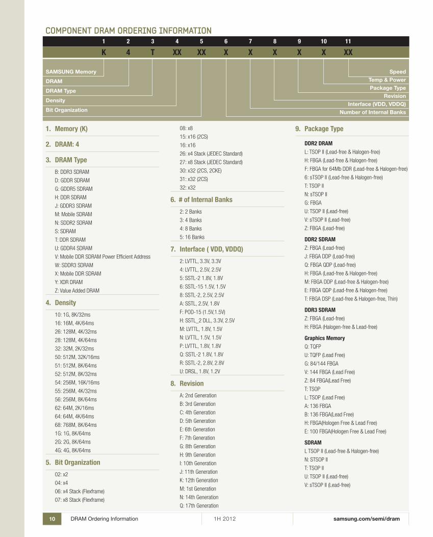
samsung.com/semi/dram10 1H 2012DRAM Ordering Information
1. Memory (K)
2. DRAM: 4
3. DRAM Type
B: DDR3 sDRAM
D: GDDR sDRAM
G: GDDR5 sDRAM
H: DDR sDRAM
J: GDDR3 sDRAM
M: Mobile sDRAM
N: sDDR2 sDRAM
s: sDRAM
t: DDR sDRAM
U: GDDR4 sDRAM
V: Mobile DDR sDRAM Power efficient Address
W: sDDR3 sDRAM
X: Mobile DDR sDRAM
Y: XDR DRAM
Z: Value Added DRAM
4. Density
10: 1G, 8K/32ms
16: 16M, 4K/64ms
26: 128M, 4K/32ms
28: 128M, 4K/64ms
32: 32M, 2K/32ms
50: 512M, 32K/16ms
51: 512M, 8K/64ms
52: 512M, 8K/32ms
54: 256M, 16K/16ms
55: 256M, 4K/32ms
56: 256M, 8K/64ms
62: 64M, 2K/16ms
64: 64M, 4K/64ms
68: 768M, 8K/64ms
1G: 1G, 8K/64ms
2G: 2G, 8K/64ms
4G: 4G, 8K/64ms
5. Bit Organization
02: x2
04: x4
06: x4 stack (Flexframe)
07: x8 stack (Flexframe)
08: x8
15: x16 (2Cs)
16: x16
26: x4 stack (JeDeC standard)
27: x8 stack (JeDeC standard)
30: x32 (2Cs, 2CKe)
31: x32 (2Cs)
32: x32
6. # of Internal Banks
2: 2 Banks
3: 4 Banks
4: 8 Banks
5: 16 Banks
7. Interface ( VDD, VDDQ)
2: LVttL, 3.3V, 3.3V
4: LVttL, 2.5V, 2.5V
5: sstL-2 1.8V, 1.8V
6: sstL-15 1.5V, 1.5V
8: sstL-2, 2.5V, 2.5V
A: sstL, 2.5V, 1.8V
F: PoD-15 (1.5V,1.5V)
H: sstL_2 DLL, 3.3V, 2.5V
M: LVttL, 1.8V, 1.5V
N: LVttL, 1.5V, 1.5V
P: LVttL, 1.8V, 1.8V
Q: sstL-2 1.8V, 1.8V
R: sstL-2, 2.8V, 2.8V
U: DRsL, 1.8V, 1.2V
8. Revision
A: 2nd Generation
B: 3rd Generation
C: 4th Generation
D: 5th Generation
e: 6th Generation
F: 7th Generation
G: 8th Generation
H: 9th Generation
I: 10th Generation
J: 11th Generation
K: 12th Generation
M: 1st Generation
N: 14th Generation
Q: 17th Generation
9. Package Type
DDR2 DRAML: tsoP II (Lead-free & Halogen-free)
H: FBGA (Lead-free & Halogen-free)
F: FBGA for 64Mb DDR (Lead-free & Halogen-free)
6: stsoP II (Lead-free & Halogen-free)
t: tsoP II
N: stsoP II
G: FBGA
U: tsoP II (Lead-free)
V: stsoP II (Lead-free)
Z: FBGA (Lead-free)
DDR2 SDRAMZ: FBGA (Lead-free)
J: FBGA DDP (Lead-free)
Q: FBGA QDP (Lead-free)
H: FBGA (Lead-free & Halogen-free)
M: FBGA DDP (Lead-free & Halogen-free)
e: FBGA QDP (Lead-free & Halogen-free)
t: FBGA DsP (Lead-free & Halogen-free, thin)
DDR3 SDRAMZ: FBGA (Lead-free)
H: FBGA (Halogen-free & Lead-free)
Graphics MemoryQ: tQFP
U: tQFP (Lead Free)
G: 84/144 FBGA
V: 144 FBGA (Lead Free)
Z: 84 FBGA(Lead Free)
t: tsoP
L: tsoP (Lead Free)
A: 136 FBGA
B: 136 FBGA(Lead Free)
H: FBGA(Hologen Free & Lead Free)
e: 100 FBGA(Hologen Free & Lead Free)
SDRAML tsoP II (Lead-free & Halogen-free)
N: stsoP II
t: tsoP II
U: tsoP II (Lead-free)
V: stsoP II (Lead-free)
COMPONENT DRAM ORDERING INFORMATION1 2 3 4 5 6 7 8 9 10 11
K 4 T XX XX X X X X X XX
SAMSUNG Memory
DRAM
DRAM Type
Density
Bit Organization
Speed
Temp & Power
Package Type
Revision
Interface (VDD, VDDQ)
Number of Internal Banks
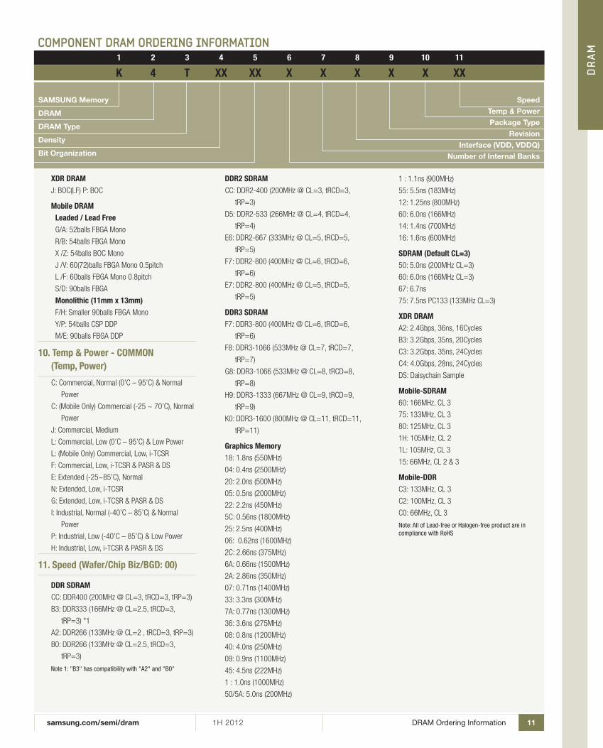
samsung.com/semi/dram 11
DR
AM
1H 2012 DRAM Ordering Information
XDR DRAMJ: BoC(LF) P: BoC
Mobile DRAMLeaded / Lead FreeG/A: 52balls FBGA Mono
R/B: 54balls FBGA Mono
X /Z: 54balls BoC Mono
J /V: 60(72)balls FBGA Mono 0.5pitch
L /F: 60balls FBGA Mono 0.8pitch
s/D: 90balls FBGA
Monolithic (11mm x 13mm)F/H: smaller 90balls FBGA Mono
Y/P: 54balls CsP DDP
M/e: 90balls FBGA DDP
10. Temp & Power - COMMON (Temp, Power)
C: Commercial, Normal (0’C – 95’C) & Normal
Power
C: (Mobile only) Commercial (-25 ~ 70’C), Normal
Power
J: Commercial, Medium
L: Commercial, Low (0’C – 95’C) & Low Power
L: (Mobile only) Commercial, Low, i-tCsR
F: Commercial, Low, i-tCsR & PAsR & Ds
e: extended (-25~85’C), Normal
N: extended, Low, i-tCsR
G: extended, Low, i-tCsR & PAsR & Ds
I: Industrial, Normal (-40’C – 85’C) & Normal
Power
P: Industrial, Low (-40’C – 85’C) & Low Power
H: Industrial, Low, i-tCsR & PAsR & Ds
11. Speed (Wafer/Chip Biz/BGD: 00)
DDR SDRAMCC: DDR400 (200MHz @ CL=3, tRCD=3, tRP=3)
B3: DDR333 (166MHz @ CL=2.5, tRCD=3,
tRP=3) *1
A2: DDR266 (133MHz @ CL=2 , tRCD=3, tRP=3)
B0: DDR266 (133MHz @ CL=2.5, tRCD=3,
tRP=3)
Note 1: "B3" has compatibility with "A2" and "B0"
DDR2 SDRAMCC: DDR2-400 (200MHz @ CL=3, tRCD=3,
tRP=3)
D5: DDR2-533 (266MHz @ CL=4, tRCD=4,
tRP=4)
e6: DDR2-667 (333MHz @ CL=5, tRCD=5,
tRP=5)
F7: DDR2-800 (400MHz @ CL=6, tRCD=6,
tRP=6)
e7: DDR2-800 (400MHz @ CL=5, tRCD=5,
tRP=5)
DDR3 SDRAMF7: DDR3-800 (400MHz @ CL=6, tRCD=6,
tRP=6)
F8: DDR3-1066 (533MHz @ CL=7, tRCD=7,
tRP=7)
G8: DDR3-1066 (533MHz @ CL=8, tRCD=8,
tRP=8)
H9: DDR3-1333 (667MHz @ CL=9, tRCD=9,
tRP=9)
K0: DDR3-1600 (800MHz @ CL=11, tRCD=11,
tRP=11)
Graphics Memory18: 1.8ns (550MHz)
04: 0.4ns (2500MHz)
20: 2.0ns (500MHz)
05: 0.5ns (2000MHz)
22: 2.2ns (450MHz)
5C: 0.56ns (1800MHz)
25: 2.5ns (400MHz)
06: 0.62ns (1600MHz)
2C: 2.66ns (375MHz)
6A: 0.66ns (1500MHz)
2A: 2.86ns (350MHz)
07: 0.71ns (1400MHz)
33: 3.3ns (300MHz)
7A: 0.77ns (1300MHz)
36: 3.6ns (275MHz)
08: 0.8ns (1200MHz)
40: 4.0ns (250MHz)
09: 0.9ns (1100MHz)
45: 4.5ns (222MHz)
1 : 1.0ns (1000MHz)
50/5A: 5.0ns (200MHz)
1 : 1.1ns (900MHz)
55: 5.5ns (183MHz)
12: 1.25ns (800MHz)
60: 6.0ns (166MHz)
14: 1.4ns (700MHz)
16: 1.6ns (600MHz)
SDRAM (Default CL=3)50: 5.0ns (200MHz CL=3)
60: 6.0ns (166MHz CL=3)
67: 6.7ns
75: 7.5ns PC133 (133MHz CL=3)
XDR DRAMA2: 2.4Gbps, 36ns, 16Cycles
B3: 3.2Gbps, 35ns, 20Cycles
C3: 3.2Gbps, 35ns, 24Cycles
C4: 4.0Gbps, 28ns, 24Cycles
Ds: Daisychain sample
Mobile-SDRAM60: 166MHz, CL 3
75: 133MHz, CL 3
80: 125MHz, CL 3
1H: 105MHz, CL 2
1L: 105MHz, CL 3
15: 66MHz, CL 2 & 3
Mobile-DDRC3: 133MHz, CL 3
C2: 100MHz, CL 3
C0: 66MHz, CL 3
Note: All of Lead-free or Halogen-free product are in compliance with RoHs
COMPONENT DRAM ORDERING INFORMATION1 2 3 4 5 6 7 8 9 10 11
K 4 T XX XX X X X X X XX
SAMSUNG Memory
DRAM
DRAM Type
Density
Bit Organization
Speed
Temp & Power
Package Type
Revision
Interface (VDD, VDDQ)
Number of Internal Banks
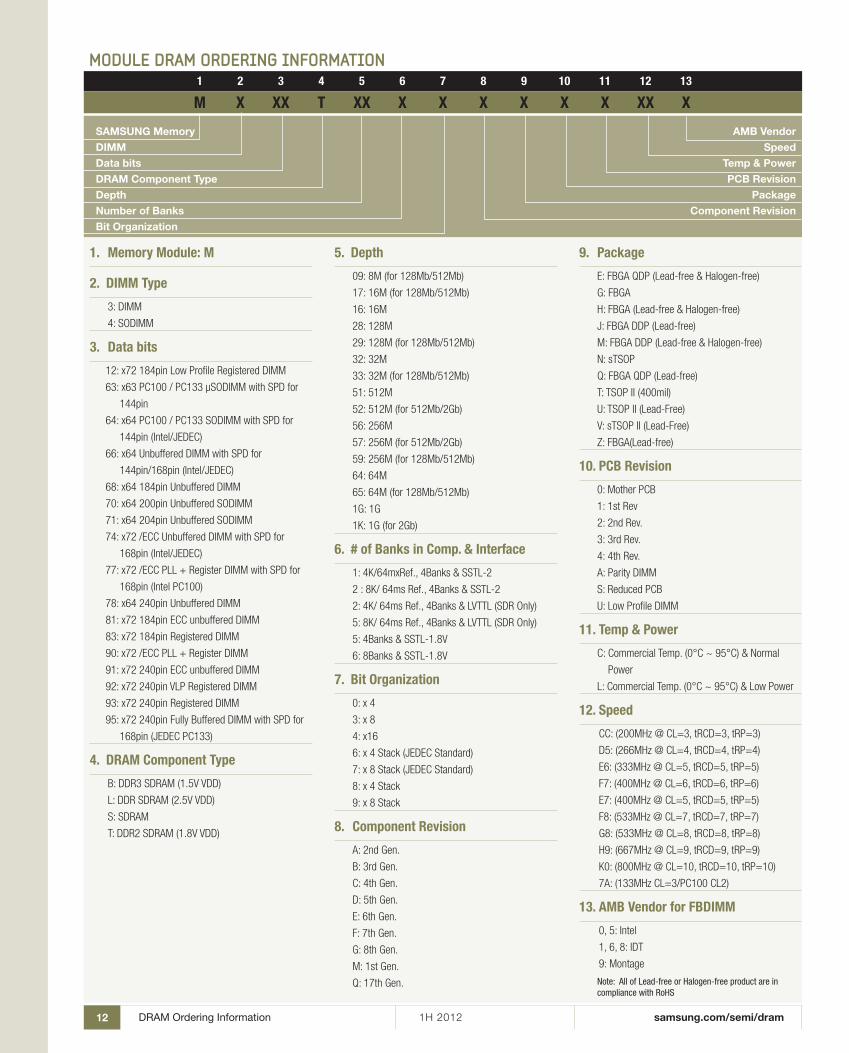
samsung.com/semi/dram12 1H 2012DRAM Ordering Information
1. Memory Module: M
2. DIMM Type
3: DIMM
4: soDIMM
3. Data bits
12: x72 184pin Low Profile Registered DIMM
63: x63 PC100 / PC133 μsoDIMM with sPD for
144pin
64: x64 PC100 / PC133 soDIMM with sPD for
144pin (Intel/JeDeC)
66: x64 Unbuffered DIMM with sPD for
144pin/168pin (Intel/JeDeC)
68: x64 184pin Unbuffered DIMM
70: x64 200pin Unbuffered soDIMM
71: x64 204pin Unbuffered soDIMM
74: x72 /eCC Unbuffered DIMM with sPD for
168pin (Intel/JeDeC)
77: x72 /eCC PLL + Register DIMM with sPD for
168pin (Intel PC100)
78: x64 240pin Unbuffered DIMM
81: x72 184pin eCC unbuffered DIMM
83: x72 184pin Registered DIMM
90: x72 /eCC PLL + Register DIMM
91: x72 240pin eCC unbuffered DIMM
92: x72 240pin VLP Registered DIMM
93: x72 240pin Registered DIMM
95: x72 240pin Fully Buffered DIMM with sPD for
168pin (JeDeC PC133)
4. DRAM Component Type
B: DDR3 sDRAM (1.5V VDD)
L: DDR sDRAM (2.5V VDD)
s: sDRAM
t: DDR2 sDRAM (1.8V VDD)
5. Depth
09: 8M (for 128Mb/512Mb)
17: 16M (for 128Mb/512Mb)
16: 16M
28: 128M
29: 128M (for 128Mb/512Mb)
32: 32M
33: 32M (for 128Mb/512Mb)
51: 512M
52: 512M (for 512Mb/2Gb)
56: 256M
57: 256M (for 512Mb/2Gb)
59: 256M (for 128Mb/512Mb)
64: 64M
65: 64M (for 128Mb/512Mb)
1G: 1G
1K: 1G (for 2Gb)
6. # of Banks in Comp. & Interface
1: 4K/64mxRef., 4Banks & sstL-2
2 : 8K/ 64ms Ref., 4Banks & sstL-2
2: 4K/ 64ms Ref., 4Banks & LVttL (sDR only)
5: 8K/ 64ms Ref., 4Banks & LVttL (sDR only)
5: 4Banks & sstL-1.8V
6: 8Banks & sstL-1.8V
7. Bit Organization
0: x 4
3: x 8
4: x16
6: x 4 stack (JeDeC standard)
7: x 8 stack (JeDeC standard)
8: x 4 stack
9: x 8 stack
8. Component Revision
A: 2nd Gen.
B: 3rd Gen.
C: 4th Gen.
D: 5th Gen.
e: 6th Gen.
F: 7th Gen.
G: 8th Gen.
M: 1st Gen.
Q: 17th Gen.
9. Package
e: FBGA QDP (Lead-free & Halogen-free)
G: FBGA
H: FBGA (Lead-free & Halogen-free)
J: FBGA DDP (Lead-free)
M: FBGA DDP (Lead-free & Halogen-free)
N: stsoP
Q: FBGA QDP (Lead-free)
t: tsoP II (400mil)
U: tsoP II (Lead-Free)
V: stsoP II (Lead-Free)
Z: FBGA(Lead-free)
10. PCB Revision
0: Mother PCB
1: 1st Rev
2: 2nd Rev.
3: 3rd Rev.
4: 4th Rev.
A: Parity DIMM
s: Reduced PCB
U: Low Profile DIMM
11. Temp & Power
C: Commercial temp. (0°C ~ 95°C) & Normal
Power
L: Commercial temp. (0°C ~ 95°C) & Low Power
12. Speed
CC: (200MHz @ CL=3, tRCD=3, tRP=3)
D5: (266MHz @ CL=4, tRCD=4, tRP=4)
e6: (333MHz @ CL=5, tRCD=5, tRP=5)
F7: (400MHz @ CL=6, tRCD=6, tRP=6)
e7: (400MHz @ CL=5, tRCD=5, tRP=5)
F8: (533MHz @ CL=7, tRCD=7, tRP=7)
G8: (533MHz @ CL=8, tRCD=8, tRP=8)
H9: (667MHz @ CL=9, tRCD=9, tRP=9)
K0: (800MHz @ CL=10, tRCD=10, tRP=10)
7A: (133MHz CL=3/PC100 CL2)
13. AMB Vendor for FBDIMM
0, 5: Intel
1, 6, 8: IDt
9: Montage
Note: All of Lead-free or Halogen-free product are in compliance with RoHs
MODULE DRAM ORDERING INFORMATION1 2 3 4 5 6 7 8 9 10 11 12 13
M X XX T XX X X X X X X XX X
SAMSUNG Memory
DIMM
Data bits
DRAM Component Type
Depth
Number of Banks
Bit Organization
AMB Vendor
Speed
Temp & Power
PCB Revision
Package
Component Revision
samsung.com/semi/flash 131H 2012
FLAS
H -
SSD
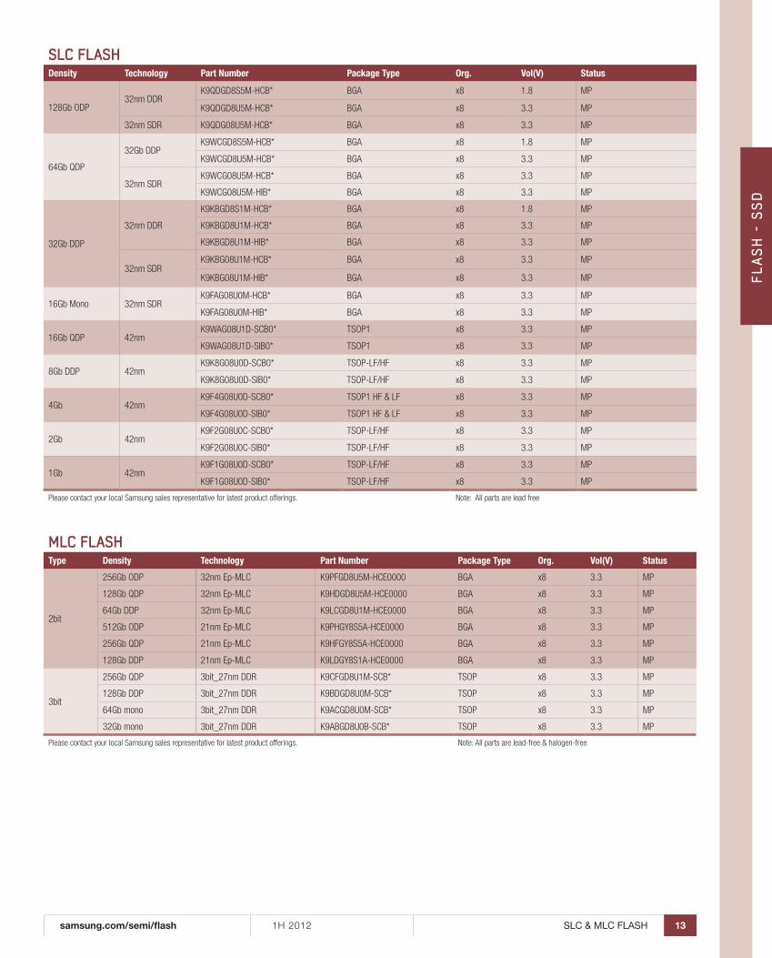
SLC & MLC FLASH
SLC FLASHDensity Technology Part Number Package Type Org. Vol(V) Status
128Gb oDP32nm DDR
K9QDGD8s5M-HCB* BGA x8 1.8 MP
K9QDGD8U5M-HCB* BGA x8 3.3 MP
32nm sDR K9QDG08U5M-HCB* BGA x8 3.3 MP
64Gb QDP
32Gb DDPK9WCGD8s5M-HCB* BGA x8 1.8 MP
K9WCGD8U5M-HCB* BGA x8 3.3 MP
32nm sDRK9WCG08U5M-HCB* BGA x8 3.3 MP
K9WCG08U5M-HIB* BGA x8 3.3 MP
32Gb DDP
32nm DDR
K9KBGD8s1M-HCB* BGA x8 1.8 MP
K9KBGD8U1M-HCB* BGA x8 3.3 MP
K9KBGD8U1M-HIB* BGA x8 3.3 MP
32nm sDRK9KBG08U1M-HCB* BGA x8 3.3 MP
K9KBG08U1M-HIB* BGA x8 3.3 MP
16Gb Mono 32nm sDRK9FAG08U0M-HCB* BGA x8 3.3 MP
K9FAG08U0M-HIB* BGA x8 3.3 MP
16Gb QDP 42nmK9WAG08U1D-sCB0* tsoP1 x8 3.3 MP
K9WAG08U1D-sIB0* tsoP1 x8 3.3 MP
8Gb DDP 42nmK9K8G08U0D-sCB0* tsoP-LF/HF x8 3.3 MP
K9K8G08U0D-sIB0* tsoP-LF/HF x8 3.3 MP
4Gb 42nmK9F4G08U0D-sCB0* tsoP1 HF & LF x8 3.3 MP
K9F4G08U0D-sIB0* tsoP1 HF & LF x8 3.3 MP
2Gb 42nmK9F2G08U0C-sCB0* tsoP-LF/HF x8 3.3 MP
K9F2G08U0C-sIB0* tsoP-LF/HF x8 3.3 MP
1Gb 42nmK9F1G08U0D-sCB0* tsoP-LF/HF x8 3.3 MP
K9F1G08U0D-sIB0* tsoP-LF/HF x8 3.3 MP
Please contact your local samsung sales representative for latest product offerings. Note: All parts are lead free
MLC FLASHType Density Technology Part Number Package Type Org. Vol(V) Status
2bit
256Gb oDP 32nm ep-MLC K9PFGD8U5M-HCe0000 BGA x8 3.3 MP
128Gb QDP 32nm ep-MLC K9HDGD8U5M-HCe0000 BGA x8 3.3 MP
64Gb DDP 32nm ep-MLC K9LCGD8U1M-HCe0000 BGA x8 3.3 MP
512Gb oDP 21nm ep-MLC K9PHGY8s5A-HCe0000 BGA x8 3.3 MP
256Gb QDP 21nm ep-MLC K9HFGY8s5A-HCe0000 BGA x8 3.3 MP
128Gb DDP 21nm ep-MLC K9LDGY8s1A-HCe0000 BGA x8 3.3 MP
3bit
256Gb QDP 3bit_27nm DDR K9CFGD8U1M-sCB* tsoP x8 3.3 MP
128Gb DDP 3bit_27nm DDR K9BDGD8U0M-sCB* tsoP x8 3.3 MP
64Gb mono 3bit_27nm DDR K9ACGD8U0M-sCB* tsoP x8 3.3 MP
32Gb mono 3bit_27nm DDR K9ABGD8U0B-sCB* tsoP x8 3.3 MP
Please contact your local samsung sales representative for latest product offerings. Note: All parts are lead-free & halogen-free
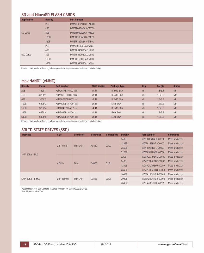
samsung.com/semi/flash14 1H 2012SD/MicroSD Flash, moviNAND & SSD
moviNAND™ (eMMC)Density Flash Part Number MMC Version Package Type Org. Vol (V) Status
2GB 16Gb*1 KLM2G1He3F-B001xxx v4.41 11.5x13 BGA x8 1.8/3.3 MP
4GB 32Gb*1 KLM4G1Fe3B-B001xxx v4.41 11.5x13 BGA x8 1.8/3.3 MP
8GB 32Gb*2 KLM8G2Fe3B-B001xxx v4.41 11.5x13 BGA x8 1.8/3.3 MP
16GB 64Gb*2 KLMAG2Ge4A-A001xxx v4.41 12x16 BGA x8 1.8/3.3 MP
16GB 32Gb*4 KLMAG4Fe3B-A001xxx v4.41 11.5x13 BGA x8 1.8/3.3 MP
32GB 64Gb*4 KLMBG4Ge4A-A001xxx v4.41 12x16 BGA x8 1.8/3.3 MP
64GB 64Gb*8 KLMCG8Ge4A-A001xxx v4.41 12x16 BGA x8 1.8/3.3 MP
Please contact your local samsung sales representative for part numbers and latest product offerings.
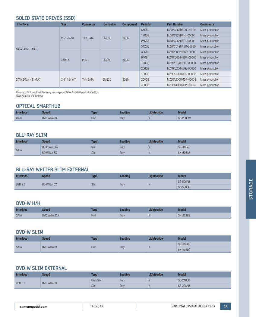
SOLID STATE DRIVES (SSD) Interface Size Connector Controller Component Density Part Number Comments
sAtA 6Gb/s - MLC
2.5" 7mmt thin sAtA PM830 32Gb
64GB MZ7PC064HADR-00000 Mass production
128GB MZ7PC128HAFU-00000 Mass production
256GB MZ7PC256HAFU-00000 Mass production
512GB MZ7PC512HAGH-00000 Mass production
msAtA PCIe PM830 32Gb
32GB MZMPC032HBCD-00000 Mass production
64GB MZMPC064HBDR-00000 Mass production
128GB MZMPC128HBFU-00000 Mass production
256GB MZMPC256HBGJ-00000 Mass production
sAtA 3Gb/s - e-MLC 2.5" 15mmt thin sAtA sM825 32Gb
100GB MZ5eA100HMDR-00003 Mass production
200GB MZ5eA200HMDR-00003 Mass production
400GB MZ5eA400HMFP-00003 Mass production
Please contact your local samsung sales representative for latest product offerings.Note: All parts are lead free
SD and MicroSD FLASH CARDSApplication Density Part Number
sD Cards
2GB MMAGF02GWFCA-2MN00
4GB MMBtF04GWBCA-QMe00
8GB MMBtF08GWBCA-RMe00
16GB MMBtF16GWBCA-RMe00
32GB MMBtF32GWBCA-sAB00
usD Cards
2GB MMAGR02GUFCA-2MN00
4GB MMBtR04GUBCA-2Me00
8GB MMBtR08GUBCA-2Me00
16GB MMBtR16GUBCA-2Me00
32GB MMBtR32GUBCA-2AB00
Please contact your local samsung sales representative for part numbers and latest product offerings.
samsung.com/semi/flash 151H 2012
FLAS
H -
SSD
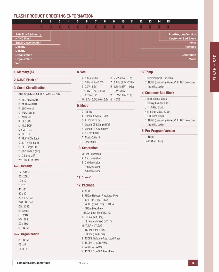
1. Memory (K)
2. NAND Flash : 9
3. Small Classification
(sLC : single Level Cell, MLC : Multi Level Cell)
7 : sLC moviNAND
8 : MLC moviNAND
F : sLC Normal
G : MLC Normal
H : MLC QDP
K : sLC DDP
L : MLC DDP
M : MLC DsP
N : sLC DsP
P : MLC 8 Die stack
Q : sLC 8 Die stack
s : sLC single sM
t : sLC sINGLe (s/B)
U : 2 stack MsP
W : sLC 4 Die stack
4~5. Density
12 : 512M
56 : 256M
1G : 1G
2G : 2G
4G : 4G
8G : 8G
AG : 16G BG :
32G CG : 64G
DG : 128G
eG : 256G
LG : 24G
NG : 96G
ZG : 48G
00 : NoNe
6~7. Organization
00 : NoNe
08 : x8
16 : x16
8. Vcc
A : 1.65V~3.6V B : 2.7V (2.5V~2.9V)
C : 5.0V (4.5V~5.5V) D : 2.65V (2.4V~2.9V)
e : 2.3V~3.6V R : 1.8V (1.65V~1.95V)
Q : 1.8V (1.7V~1.95V) t : 2.4V~3.0V
U : 2.7V~3.6V V : 3.3V (3.0V~3.6V)
W : 2.7V~5.5V, 3.0V~5.5V 0 : NoNe
9. Mode
0 : Normal
1 : Dual nCe & Dual R/nB
3 : tri /Ce & tri R/B
4 : Quad nCe & single R/nB
5 : Quad nCe & Quad R/nB
9 : 1st block otP
A : Mask option 1
L : Low grade
10. Generation
M : 1st Generation
A : 2nd Generation
B : 3rd Generation
C : 4th Generation
D : 5th Generation
11. “ ----”
12. Package
A : CoB
B : FBGA (Halogen-Free, Lead-Free)
C : CHIP BIZ D : 63-tBGA
F : WsoP (Lead-Free) G : FBGA
H : tBGA (Lead-Free)
I : ULGA (Lead-Free) (12*17)
J : FBGA (Lead-Free)
L : ULGA (Lead-Free) (14*18)
M : tLGA N : tLGA2
P : tsoP1 (Lead-Free)
Q : tsoP2 (Lead-Free)
s : tsoP1 (Halogen-Free, Lead-Free)
t : tsoP2 U : CoB (MMC)
V : WsoP W : Wafer
Y : tsoP1 Z : WeLP (Lead-Free)
13. Temp
C : Commercial I : Industrial
0 : NoNe (Containing Wafer, CHIP, BIZ, exception
handling code)
14. Customer Bad Block
B : Include Bad Block
D : Daisychain sample
L : 1~5 Bad Block
N : ini. 0 blk, add. 10 blk
s : All Good Block
0 : NoNe (Containing Wafer, CHIP, BIZ, exception
handling code)
15. Pre-Program Version
0 : None
serial (1~9, A~Z)
FLASH PRODUCT ORDERING INFORMATION1 2 3 4 5 6 7 8 9 10 11 12 13 14 15
K 9 X X X X X X X X - X X X X
SAMSUNG Memory
NAND Flash
Small Classification
Density
Density
Organization
Organization
Vcc
Pre-Program Version
Customer Bad Block
Temp
Package
---
Generation
Mode
samsung.com/semi/mcp16 1H 2012Multi-Chip Packages
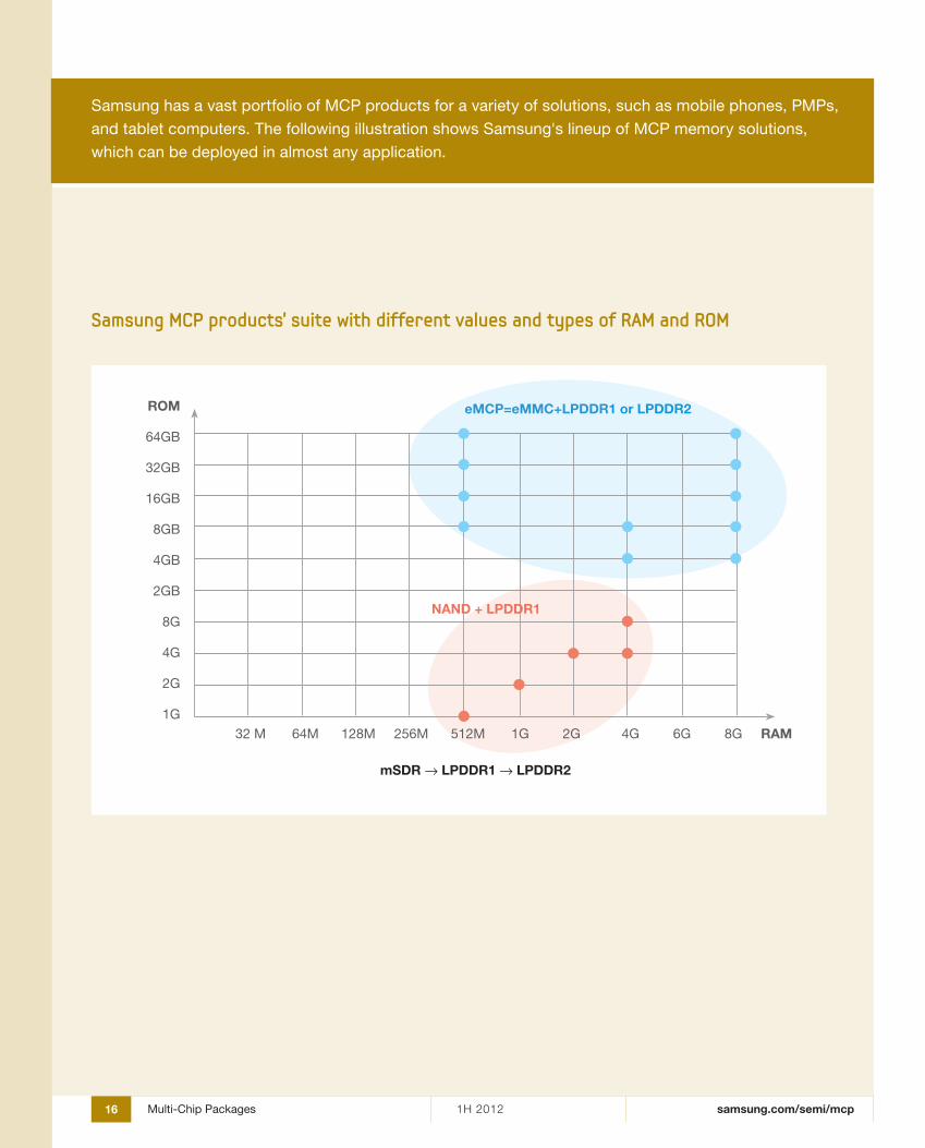
Samsung has a vast portfolio of MCP products for a variety of solutions, such as mobile phones, PMPs, and tablet computers. The following illustration shows Samsung's lineup of MCP memory solutions, which can be deployed in almost any application.
eMCP=eMMC+LPDDR1 or LPDDR2
NAND + LPDDR1
mSDR → LPDDR1 → LPDDR2
ROM
64GB
32GB
16GB
8GB
4GB
2GB
8G
4G
2G
1G32 M 64M 128M 256M 512M 1G 2G 4G 6G 8G RAM
Samsung MCP products' suite with different values and types of RAM and ROM
MC
P
samsung.com/semi/mcp 171H 2012 Multi-Chip Packages
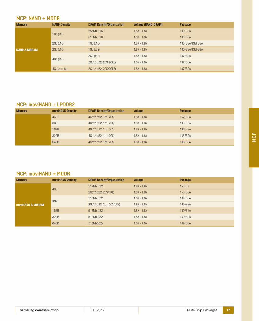
MCP: NAND + MDDRMemory NAND Density DRAM Density/Organization Voltage (NAND-DRAM) Package
NAND & MDRAM
1Gb (x16)256Mb (x16) 1.8V - 1.8V 130FBGA
512Mb (x16) 1.8V - 1.8V 130FBGA
2Gb (x16) 1Gb (x16) 1.8V - 1.8V 130FBGA/137FBGA
2Gb (x16) 1Gb (x32) 1.8V - 1.8V 130FBGA/137FBGA
4Gb (x16)2Gb (x32) 1.8V - 1.8V 137FBGA
2Gb*2 (x32, 2Cs/2CKe) 1.8V - 1.8V 137FBGA
4Gb*2 (x16) 2Gb*2 (x32, 2Cs/2CKe) 1.8V - 1.8V 137FBGA
MCP: moviNAND + LPDDR2Memory moviNAND Density DRAM Density/Organization Voltage Package
4GB 4Gb*2 (x32, 1ch, 2Cs) 1.8V - 1.8V 162FBGA
8GB 4Gb*2 (x32, 1ch, 2Cs) 1.8V - 1.8V 186FBGA
16GB 4Gb*2 (x32, 1ch, 2Cs) 1.8V - 1.8V 186FBGA
32GB 4Gb*2 (x32, 1ch, 2Cs) 1.8V - 1.8V 186FBGA
64GB 4Gb*2 (x32, 1ch, 2Cs) 1.8V - 1.8V 186FBGA
MCP: moviNAND + MDDR Memory moviNAND Density DRAM Density/Organization Voltage Package
moviNAND & MDRAM
4GB512Mb (x32) 1.8V - 1.8V 153FBG
2Gb*2 (x32, 2Cs/CKe) 1.8V - 1.8V 153FBGA
8GB512Mb (x32) 1.8V - 1.8V 169FBGA
2Gb*2 (x32, 2ch, 2Cs/CKe) 1.8V - 1.8V 169FBGA
16GB 512Mb (x32) 1.8V - 1.8V 169FBGA
32GB 512Mb (x32) 1.8V - 1.8V 169FBGA
64GB 512Mb(x32) 1.8V - 1.8V 169FBGA
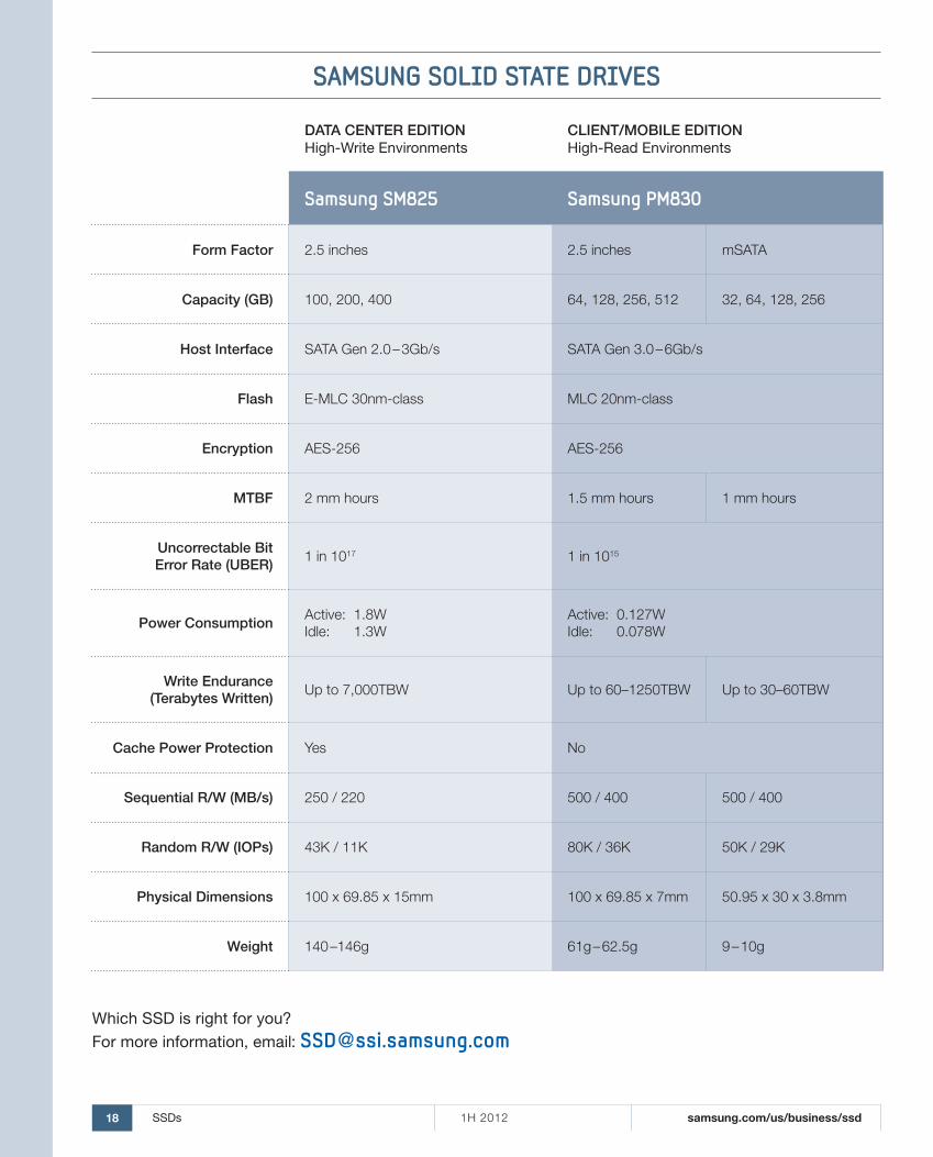
18 1H 2012SSDs samsung.com/us/business/ssd
SAMSUNG SOLID STATE DRIVES
Data Center eDItIOnHigh-Write Environments
ClIent/MObIle eDItIOn High-Read Environments
Samsung SM825 Samsung PM830
Form Factor 2.5 inches 2.5 inches mSATA
Capacity (Gb) 100, 200, 400 64, 128, 256, 512 32, 64, 128, 256
Host Interface SATA Gen 2.0 – 3Gb/s SATA Gen 3.0 – 6Gb/s
Flash E-MLC 30nm-class MLC 20nm-class
encryption AES-256 AES-256
MtbF 2 mm hours 1.5 mm hours 1 mm hours
Uncorrectable bit error rate (Uber)
1 in 1017 1 in 1015
Power ConsumptionActive: 1.8WIdle: 1.3W
Active: 0.127WIdle: 0.078W
Write endurance (terabytes Written)
Up to 7,000TBW Up to 60–1250TBW Up to 30–60TBW
Cache Power Protection Yes No
Sequential r/W (Mb/s) 250 / 220 500 / 400 500 / 400
random r/W (IOPs) 43K / 11K 80K / 36K 50K / 29K
Physical Dimensions 100 x 69.85 x 15mm 100 x 69.85 x 7mm 50.95 x 30 x 3.8mm
Weight 140 –146g 61g – 62.5g 9 – 10g
Which SSD is right for you? For more information, email: [email protected]
191H 2012
STO
RAG
E
OPTICAL SMARTHUB & DVDsamsungodd.com
DVD-W H/HInterface Speed Type Loading Lightscribe Model
sAtA DVD Write 22X H/H tray X sH-222BB
DVD-W SLIMInterface Speed Type Loading Lightscribe Model
sAtA DVD Write 8X slim tray XsN-208BB
sN-208DB
DVD-W SLIM ExTERNALInterface Speed Type Loading Lightscribe Model
UsB 2.0 DVD Write 8XUltra slim tray X se-218BB
slim tray X se-208AB
OPTICAL SMARTHUBInterface Speed Type Loading Lightscribe Model
Wi-Fi DVD Write 8X slim tray X se-208BW
BLU-RAY SLIMInterface Speed Type Loading Lightscribe Model
sAtABD Combo 6X slim tray X sN-406AB
BD Writer 6X slim tray X sN-506AB
BLU-RAY WRITER SLIM ExTERNALInterface Speed Type Loading Lightscribe Model
UsB 2.0 BD Writer 6X slim tray Xse-506AB
se-506BB
SOLID STATE DRIVES (SSD) Interface Size Connector Controller Component Density Part Number Comments
sAtA 6Gb/s - MLC
2.5" 7mmt thin sAtA PM830 32Gb
64GB MZ7PC064HADR-00000 Mass production
128GB MZ7PC128HAFU-00000 Mass production
256GB MZ7PC256HAFU-00000 Mass production
512GB MZ7PC512HAGH-00000 Mass production
msAtA PCIe PM830 32Gb
32GB MZMPC032HBCD-00000 Mass production
64GB MZMPC064HBDR-00000 Mass production
128GB MZMPC128HBFU-00000 Mass production
256GB MZMPC256HBGJ-00000 Mass production
sAtA 3Gb/s - e-MLC 2.5" 15mmt thin sAtA sM825 32Gb
100GB MZ5eA100HMDR-00003 Mass production
200GB MZ5eA200HMDR-00003 Mass production
400GB MZ5eA400HMFP-00003 Mass production
Please contact your local samsung sales representative for latest product offerings.Note: All parts are lead free
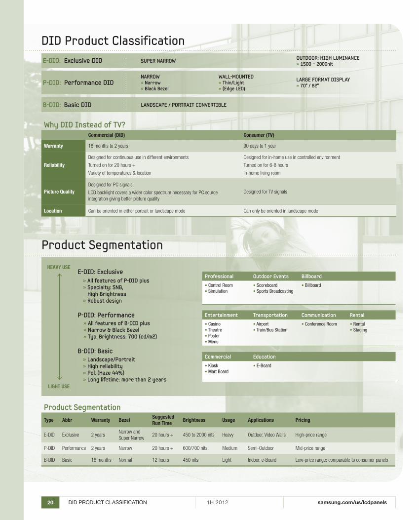
samsung.com/us/lcdpanels20 1H 2012DID PRODUCT CLASSIFICATION
DID Product ClassificationE-DID: Exclusive DID
NARROW» Narrow» Black Bezel
LANDSCAPE / PORTRAIT CONVERTIBLE
WALL-MOUNTED» Thin/Light» (Edge LED)
OUTDOOR: HIGH LUMINANCE» 1500 – 2000nitSUPER NARROW
LARGE FORMAT DISPLAY» 70” / 82”P-DID: Performance DID
B-DID: Basic DID
Why DID Instead of TV? Commercial (DID) Consumer (TV)
Warranty 18 months to 2 years 90 days to 1 year
Reliability
Designed for continuous use in different environments
Turned on for 20 hours +
Variety of temperatures & location
Designed for in-home use in controlled environment
Turned on for 6-8 hours
In-home living room
Picture QualityDesigned for PC signals
LCD backlight covers a wider color spectrum necessary for PC source integration giving better picture quality
Designed for TV signals
Location Can be oriented in either portrait or landscape mode Can only be oriented in landscape mode
Product SegmentationType Abbr Warranty Bezel
Suggested Run Time
Brightness Usage Applications Pricing
E-DID Exclusive 2 yearsNarrow and Super Narrow
20 hours + 450 to 2000 nits Heavy Outdoor, Video Walls High-price range
P-DID Performance 2 years Narrow 20 hours + 600/700 nits Medium Semi-Outdoor Mid-price range
B-DID Basic 18 months Normal 12 hours 450 nits Light Indoor, e-Board Low-price range; comparable to consumer panels
Product SegmentationHEAVY USE
LIGHT USE
E-DID: Exclusive» All features of P-DID plus» Specialty: SNB, High Brightness» Robust design
P-DID: Performance» All features of B-DID plus» Narrow & Black Bezel » Typ. Brightness: 700 (cd/m2)
B-DID: Basic» Landscape/Portrait» High reliability » Pol. (Haze 44%)» Long lifetime: more than 2 years
Professional Outdoor Events Billboard
• Control Room• simulation
• scoreboard• sports Broadcasting
• Billboard
Entertainment Transportation Communication Rental
• Casino• Theatre • Poster• Menu
• Airport• Train/Bus station
• Conference Room • Rental• staging
Commercial Education
• Kiosk• Mart Board
• E-Board
LCD
samsung.com/us/lcdpanels 211H 2012 DID PANEL LINEUP
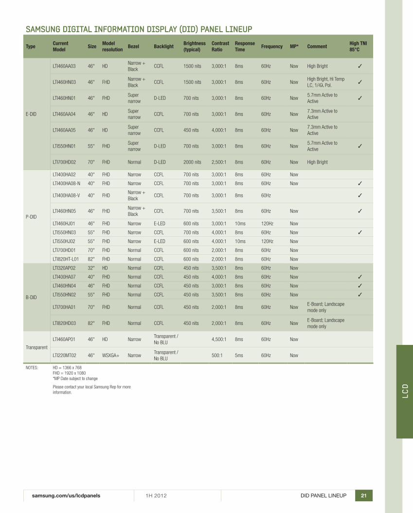
SAMSUNG DIGITAL INFORMATION DISPLAY (DID) PANEL LINEUP
TypeCurrent Model
SizeModel resolution
Bezel BacklightBrightness (typical)
Contrast Ratio
Response Time
Frequency MP* CommentHigh TNI 85°C
e-DID
LtI460AA03 46" HDNarrow + Black
CCFL 1500 nits 3,000:1 8ms 60Hz Now High Bright
LtI460HN03 46" FHDNarrow + Black
CCFL 1500 nits 3,000:1 8ms 60Hz NowHigh Bright, Hi temp LC, 1/4λ Pol.
LtI460HN01 46" FHDsuper narrow
D-LeD 700 nits 3,000:1 8ms 60Hz Now5.7mm Active to Active
LtI460AA04 46" HDsuper narrow
CCFL 700 nits 3,000:1 8ms 60Hz Now7.3mm Active to Active
LtI460AA05 46" HDsuper narrow
CCFL 450 nits 4,000:1 8ms 60Hz Now7.3mm Active to Active
LtI550HN01 55" FHDsuper narrow
D-LeD 700 nits 3,000:1 8ms 60Hz Now5.7mm Active to Active
LtI700HD02 70" FHD Normal D-LeD 2000 nits 2,500:1 8ms 60Hz Now High Bright
P-DID
LtI400HA02 40" FHD Narrow CCFL 700 nits 3,000:1 8ms 60Hz Now
LtI400HA08-N 40" FHD Narrow CCFL 700 nits 3,000:1 8ms 60Hz Now
LtI400HA08-V 40" FHDNarrow + Black
CCFL 700 nits 3,000:1 8ms 60Hz
LtI460HN05 46" FHDNarrow + Black
CCFL 700 nits 3,500:1 8ms 60Hz Now
LtI460HJ01 46" FHD Narrow e-LeD 600 nits 3,000:1 10ms 120Hz Now
LtI550HN03 55" FHD Narrow CCFL 700 nits 4,000:1 8ms 60Hz Now
LtI550HJ02 55" FHD Narrow e-LeD 600 nits 4,000:1 10ms 120Hz Now
LtI700HD01 70" FHD Normal CCFL 600 nits 2,000:1 8ms 60Hz Now
LtI820Ht-L01 82" FHD Normal CCFL 600 nits 2,000:1 8ms 60Hz Now
B-DID
LtI320AP02 32" HD Normal CCFL 450 nits 3,500:1 8ms 60Hz Now
LtI400HA07 40" FHD Normal CCFL 450 nits 4,000:1 8ms 60Hz Now
LtI460HN04 46" FHD Normal CCFL 450 nits 3,000:1 8ms 60Hz Now
LtI550HN02 55" FHD Normal CCFL 450 nits 3,500:1 8ms 60Hz Now
LtI700HA01 70" FHD Normal CCFL 450 nits 2,000:1 8ms 60Hz Nowe-Board; Landscape mode only
LtI820HD03 82" FHD Normal CCFL 450 nits 2,000:1 8ms 60Hz Nowe-Board; Landscape mode only
transparent
LtI460AP01 46" HD Narrowtransparent / No BLU
4,500:1 8ms 60Hz Now
LtI220Mt02 46" WsXGA+ Narrowtransparent / No BLU
500:1 5ms 60Hz Now
Notes: HD = 1366 x 768 FHD = 1920 x 1080 *MP Date subject to change
Please contact your local samsung Rep for more information.
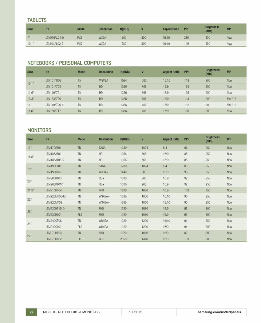
samsung.com/us/lcdpanels22 1H 2012TABLETS, NOTEBOOKS & MONITORS
TABLETSSize PN Mode Resolution H(RGB) V Aspect Ratio PPI
Brightness (nits)
MP
7" LtN070AL01-0 PLs WXGA 1280 800 16:10 216 400 Now
10.1" LtL101AL02-D PLs WXGA 1280 800 16:10 149 400 Now
NOTEBOOKS / PERSONAL COMPUTERSSize PN Mode Resolution H(RGB) V Aspect Ratio PPI
Brightness (nits)
MP
10.1"LtN101Nt08 tN WsVGA 1024 600 16:10 118 200 Now
LtN101At03 tN HD 1366 768 16:9 155 200 Now
11.6" LtN116At01 tN HD 1366 768 16:9 135 200 Now
13.3" LtN133At20 tN HD 1366 768 16:9 118 200 Mar '12
14" LtN140At20-6 tN HD 1366 768 16:9 112 200 Mar '12
15.6" LtN156At17 tN HD 1366 768 16:9 100 200 Now
MONITORSSize PN Mode Resolution H(RGB) V Aspect Ratio PPI
Brightness (nits)
MP
17" LtM170et01 tN sXGA 1280 1024 5:4 96 250 Now
18.5"LtM185At01 tN HD 1366 768 16:9 85 250 Now
LtM185At05-Q tN HD 1366 768 16:9 85 250 Now
19"LtM190et01 tN sXGA 1280 1024 5:4 86 250 Now
LtM190Bt07 tN WXGA+ 1440 900 16:9 96 250 Now
20"LtM200Kt03 tN HD+ 1600 900 16:9 92 250 Now
LtM200Kt010 tN HD+ 1600 900 16:9 92 250 Now
21.5" LtM215Ht04 tN FHD 1920 1080 16:9 103 250 Now
22"LtM220Mt05-M tN WsXGA+ 1680 1050 16:10 90 250 Now
LtM220Mt09 tN WsXGA+ 1680 1050 16:10 90 250 Now
23"LtM230Ht10-Q tN FHD 1920 1080 16:9 96 300 Now
LtM230HL01 PLs FHD 1920 1080 16:9 96 300 Now
24"LtM240Ct06 tN WUXGA 1920 1200 16:10 94 250 Now
LtM240CL01 PLs WUXGA 1920 1200 16:9 94 300 Now
27"LtM270Ht03 tN FHD 1920 1080 16:9 82 300 Now
LtM270DL02 PLs QHD 2560 1440 16:9 109 300 Now
samsung.com/us/oem-solutions 231H 2012 CO
NTA
CTS
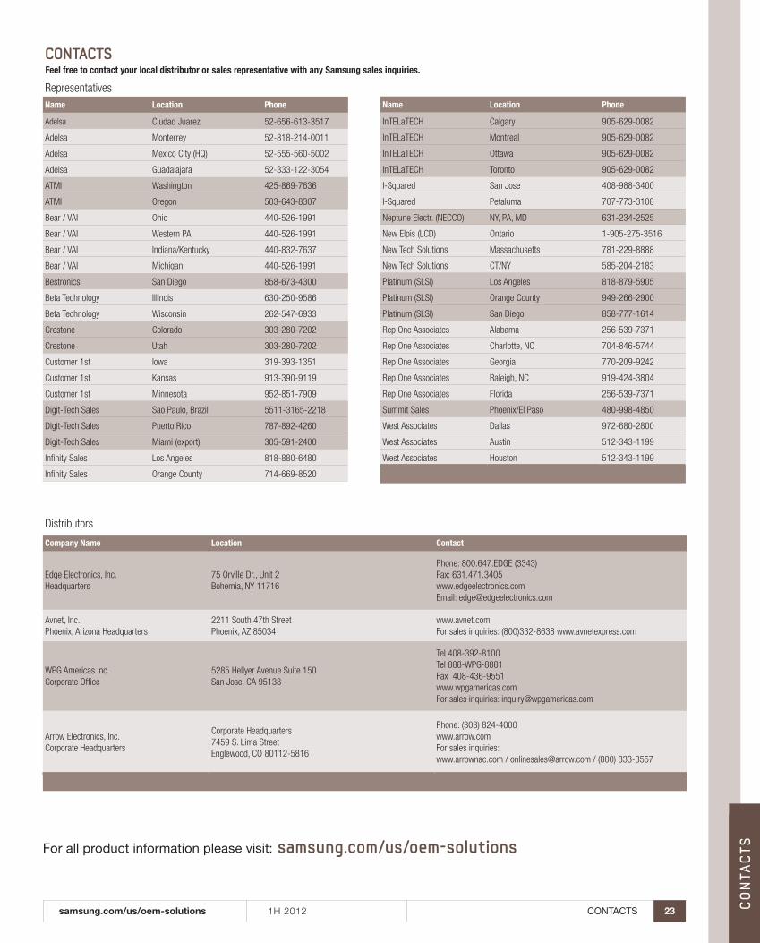
CONTACTS
RepresentativesName Location Phone
Adelsa Ciudad Juarez 52-656-613-3517
Adelsa Monterrey 52-818-214-0011
Adelsa Mexico City (HQ) 52-555-560-5002
Adelsa Guadalajara 52-333-122-3054
AtMI Washington 425-869-7636
AtMI oregon 503-643-8307
Bear / VAI ohio 440-526-1991
Bear / VAI Western PA 440-526-1991
Bear / VAI Indiana/Kentucky 440-832-7637
Bear / VAI Michigan 440-526-1991
Bestronics san Diego 858-673-4300
Beta technology Illinois 630-250-9586
Beta technology Wisconsin 262-547-6933
Crestone Colorado 303-280-7202
Crestone Utah 303-280-7202
Customer 1st Iowa 319-393-1351
Customer 1st Kansas 913-390-9119
Customer 1st Minnesota 952-851-7909
Digit-tech sales sao Paulo, Brazil 5511-3165-2218
Digit-tech sales Puerto Rico 787-892-4260
Digit-tech sales Miami (export) 305-591-2400
Infinity sales Los Angeles 818-880-6480
Infinity sales orange County 714-669-8520
Name Location Phone
InteLateCH Calgary 905-629-0082
InteLateCH Montreal 905-629-0082
InteLateCH ottawa 905-629-0082
InteLateCH toronto 905-629-0082
I-squared san Jose 408-988-3400
I-squared Petaluma 707-773-3108
Neptune electr. (NeCCo) NY, PA, MD 631-234-2525
New elpis (LCD) ontario 1-905-275-3516
New tech solutions Massachusetts 781-229-8888
New tech solutions Ct/NY 585-204-2183
Platinum (sLsI) Los Angeles 818-879-5905
Platinum (sLsI) orange County 949-266-2900
Platinum (sLsI) san Diego 858-777-1614
Rep one Associates Alabama 256-539-7371
Rep one Associates Charlotte, NC 704-846-5744
Rep one Associates Georgia 770-209-9242
Rep one Associates Raleigh, NC 919-424-3804
Rep one Associates Florida 256-539-7371
summit sales Phoenix/el Paso 480-998-4850
West Associates Dallas 972-680-2800
West Associates Austin 512-343-1199
West Associates Houston 512-343-1199
Distributors
Company Name Location Contact
edge electronics, Inc.Headquarters
75 orville Dr., Unit 2Bohemia, NY 11716
Phone: 800.647.eDGe (3343)Fax: 631.471.3405www.edgeelectronics.comemail: [email protected]
Avnet, Inc.Phoenix, Arizona Headquarters
2211 south 47th streetPhoenix, AZ 85034
www.avnet.comFor sales inquiries: (800)332-8638 www.avnetexpress.com
WPG Americas Inc.Corporate office
5285 Hellyer Avenue suite 150 san Jose, CA 95138
tel 408-392-8100tel 888-WPG-8881Fax 408-436-9551www.wpgamericas.comFor sales inquiries: [email protected]
Arrow electronics, Inc. Corporate Headquarters
Corporate Headquarters7459 s. Lima streetenglewood, Co 80112-5816
Phone: (303) 824-4000www.arrow.comFor sales inquiries: www.arrownac.com / [email protected] / (800) 833-3557
For all product information please visit: samsung.com/us/oem-solutions
Feel free to contact your local distributor or sales representative with any Samsung sales inquiries.
CONTACTS
Disclaimer: The information in this publication has been carefully checked and is believed to be accurate at the time of publication. Samsung assumes no responsibility, however, for possible errors or omissions, or for any consequences resulting from the use of the information contained herein. Samsung reserves the right to make changes in its products or product specifications with the intent to improve function or design at any time and without notice and is not required to update this documentation to reflect such changes. This publication does not convey to a purchaser of semiconductor devices described herein any license under the patent rights of Samsung or others. Samsung makes no warranty, representation, or guarantee regarding the suitability of its products for any particular purpose, nor does Samsung assume any liability arising out of the application or use of any product or circuit and specifically disclaims any and all liability, including without limitation any consequential or incidental damages.
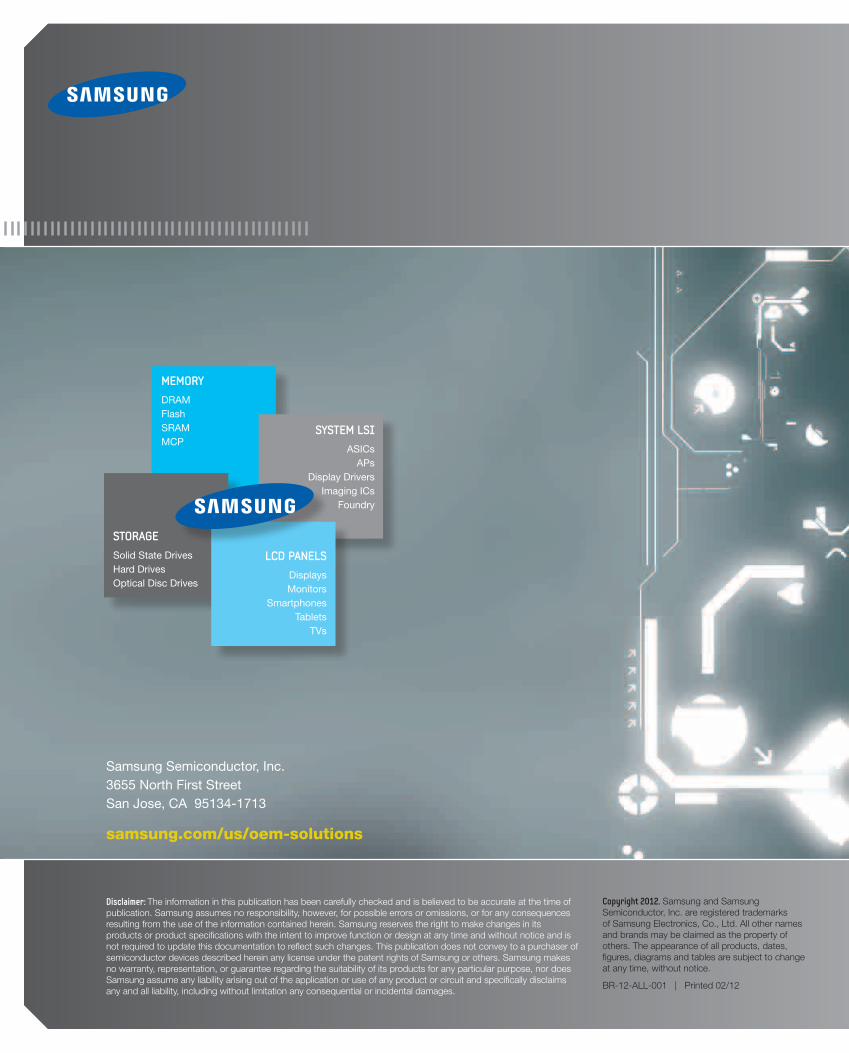
Samsung Semiconductor, Inc. 3655 North First Street San Jose, CA 95134-1713
samsung.com/us/oem-solutions
Copyright 2012. Samsung and Samsung Semiconductor, Inc. are registered trademarks of Samsung Electronics, Co., Ltd. All other names and brands may be claimed as the property of others. The appearance of all products, dates, figures, diagrams and tables are subject to change at any time, without notice.
BR-12-ALL-001 | Printed 02/12
MEMORYDRAMFlashSRAMMCP
SYSTEM LSIASICs
APs Display Drivers
Imaging ICs Foundry
STORAGESolid State Drives Hard Drives Optical Disc Drives
LCD PANELSDisplays Monitors
SmartphonesTablets
TVs
![4Gb E-die DDR3 SDRAM x16 - samsung.com · - 5 - K4B4G1646E datasheet DDR3 SDRAM Rev. 1.01 1. Ordering Information [ Table 1 ] Samsung 4Gb DDR3 E-die ordering information table NOTE:](https://img.pdfslide.us/doc/110x75/5e15e846c6296e58e6146f8b/4gb-e-die-ddr3-sdram-x16-5-k4b4g1646e-datasheet-ddr3-sdram-rev-101-1-ordering.jpg)


![4Gb Q-die DDR3 SDRAM - Samsung · Table Of Contents 4Gb Q-die DDR3 SDRAM 1. ... DDR3 SDRAM Addressing ... [ Table 1 ] Samsung 4Gb DDR3 Q-die ordering information table](https://img.pdfslide.us/doc/110x75/5ad5dbf67f8b9a5c638d9a46/4gb-q-die-ddr3-sdram-of-contents-4gb-q-die-ddr3-sdram-1-ddr3-sdram-addressing.jpg)