Embed Size (px)
Citation preview
PRODUCT SELECTION GUIDE2016
SMD RESISTORS + MLCC
SMD CERAMIC EMI FILTER CAPACITORS - X2Y ®
WIRELESS COMPONENTS
MULTILAYER CHIP VARISTORSw
ww
.yag
eo.c
om

3
Part numbering system and ordering
You can order components from this catalogue in two ways. Both ways give logistic and packing information.
• Clear text ordering codeThis unique number is an easily-readable code.- 15 digits code (PHYCOMP CTC )- 14 to 17 digits code (GLOBAL PART NUMBER for both Yageo and Phycomp branded products)
• 12 digits ordering codeThis unique 12NC number forms the basis of the Phycomp logistic system.
You will find details for ordering in the "Ordering" section next to each selection chart.
Minimum shipment quantities, prices and delivering details can be obtained from the Yageo sales organization in your country or from one of our franchised distributors.
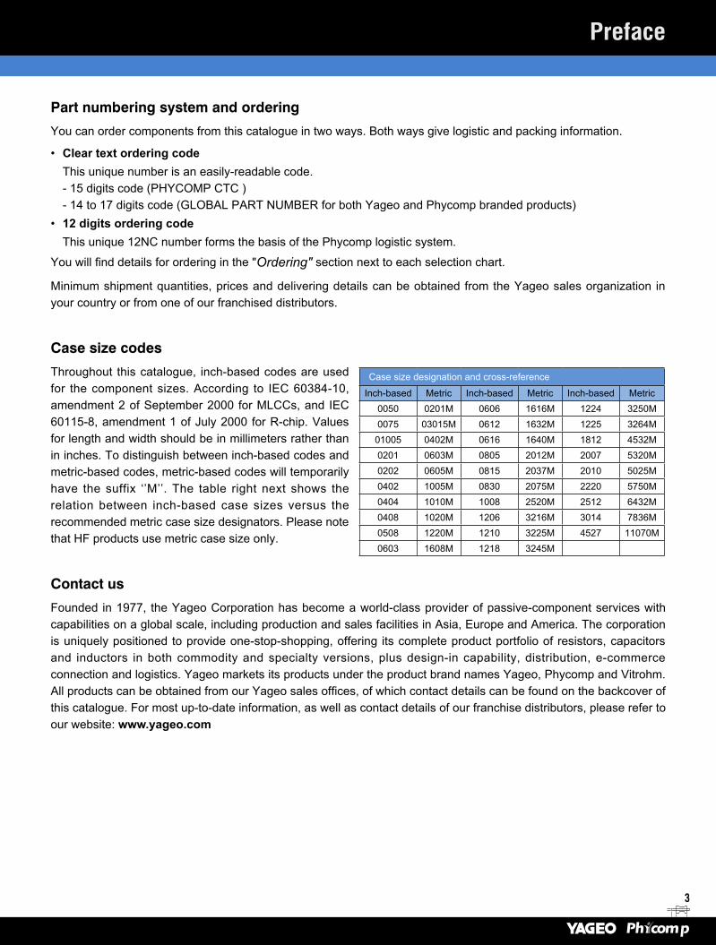
Case size codes
Throughout this catalogue, inch-based codes are used for the component sizes. According to IEC 60384-10, amendment 2 of September 2000 for MLCCs, and IEC 60115-8, amendment 1 of July 2000 for R-chip. Values for length and width should be in millimeters rather than in inches. To distinguish between inch-based codes and metric-based codes, metric-based codes will temporarily have the suffix ‘’M’’. The table right next shows the relation between inch-based case sizes versus the recommended metric case size designators. Please note that HF products use metric case size only.
Contact us
Founded in 1977, the Yageo Corporation has become a world-class provider of passive-component services with capabilities on a global scale, including production and sales facilities in Asia, Europe and America. The corporation is uniquely positioned to provide one-stop-shopping, offering its complete product portfolio of resistors, capacitors and inductors in both commodity and specialty versions, plus design-in capability, distribution, e-commerce connection and logistics. Yageo markets its products under the product brand names Yageo, Phycomp and Vitrohm. All products can be obtained from our Yageo sales offices, of which contact details can be found on the backcover of this catalogue. For most up-to-date information, as well as contact details of our franchise distributors, please refer to our website: www.yageo.com
Case size designation and cross-reference
Inch-based Metric Inch-based Metric Inch-based Metric0050 0201M 0606 1616M 1224 3250M0075 03015M 0612 1632M 1225 3264M
01005 0402M 0616 1640M 1812 4532M0201 0603M 0805 2012M 2007 5320M0202 0605M 0815 2037M 2010 5025M0402 1005M 0830 2075M 2220 5750M0404 1010M 1008 2520M 2512 6432M0408 1020M 1206 3216M 3014 7836M0508 1220M 1210 3225M 4527 11070M0603 1608M 1218 3245M
Preface
4
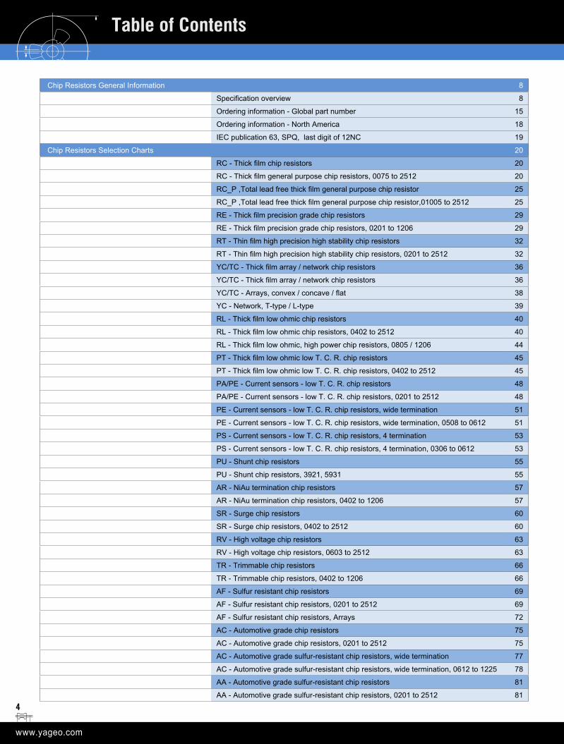
Table of Contents
Chip Resistors General Information 8
Specification overview 8
Ordering information - Global part number 15
Ordering information - North America 18
IEC publication 63, SPQ, last digit of 12NC 19
Chip Resistors Selection Charts 20
RC - Thick film chip resistors 20
RC - Thick film general purpose chip resistors, 0075 to 2512 20
RC_P ,Total lead free thick film general purpose chip resistor 25
RC_P ,Total lead free thick film general purpose chip resistor,01005 to 2512 25
RE - Thick film precision grade chip resistors 29
RE - Thick film precision grade chip resistors, 0201 to 1206 29
RT - Thin film high precision high stability chip resistors 32
RT - Thin film high precision high stability chip resistors, 0201 to 2512 32
YC/TC - Thick film array / network chip resistors 36
YC/TC - Thick film array / network chip resistors 36
YC/TC - Arrays, convex / concave / flat 38
YC - Network, T-type / L-type 39
RL - Thick film low ohmic chip resistors 40
RL - Thick film low ohmic chip resistors, 0402 to 2512 40
RL - Thick film low ohmic, high power chip resistors, 0805 / 1206 44
PT - Thick film low ohmic low T. C. R. chip resistors 45
PT - Thick film low ohmic low T. C. R. chip resistors, 0402 to 2512 45
PA/PE - Current sensors - low T. C. R. chip resistors 48
PA/PE - Current sensors - low T. C. R. chip resistors, 0201 to 2512 48
PE - Current sensors - low T. C. R. chip resistors, wide termination 51
PE - Current sensors - low T. C. R. chip resistors, wide termination, 0508 to 0612 51
PS - Current sensors - low T. C. R. chip resistors, 4 termination 53
PS - Current sensors - low T. C. R. chip resistors, 4 termination, 0306 to 0612 53
PU - Shunt chip resistors 55
PU - Shunt chip resistors, 3921, 5931 55
AR - NiAu termination chip resistors 57
AR - NiAu termination chip resistors, 0402 to 1206 57
SR - Surge chip resistors 60
SR - Surge chip resistors, 0402 to 2512 60
RV - High voltage chip resistors 63
RV - High voltage chip resistors, 0603 to 2512 63
TR - Trimmable chip resistors 66
TR - Trimmable chip resistors, 0402 to 1206 66
AF - Sulfur resistant chip resistors 69
AF - Sulfur resistant chip resistors, 0201 to 2512 69
AF - Sulfur resistant chip resistors, Arrays 72
AC - Automotive grade chip resistors 75
AC - Automotive grade chip resistors, 0201 to 2512 75
AC - Automotive grade sulfur-resistant chip resistors, wide termination 77
AC - Automotive grade sulfur-resistant chip resistors, wide termination, 0612 to 1225 78
AA - Automotive grade sulfur-resistant chip resistors 81
AA - Automotive grade sulfur-resistant chip resistors, 0201 to 2512 81
5
Table of Contents
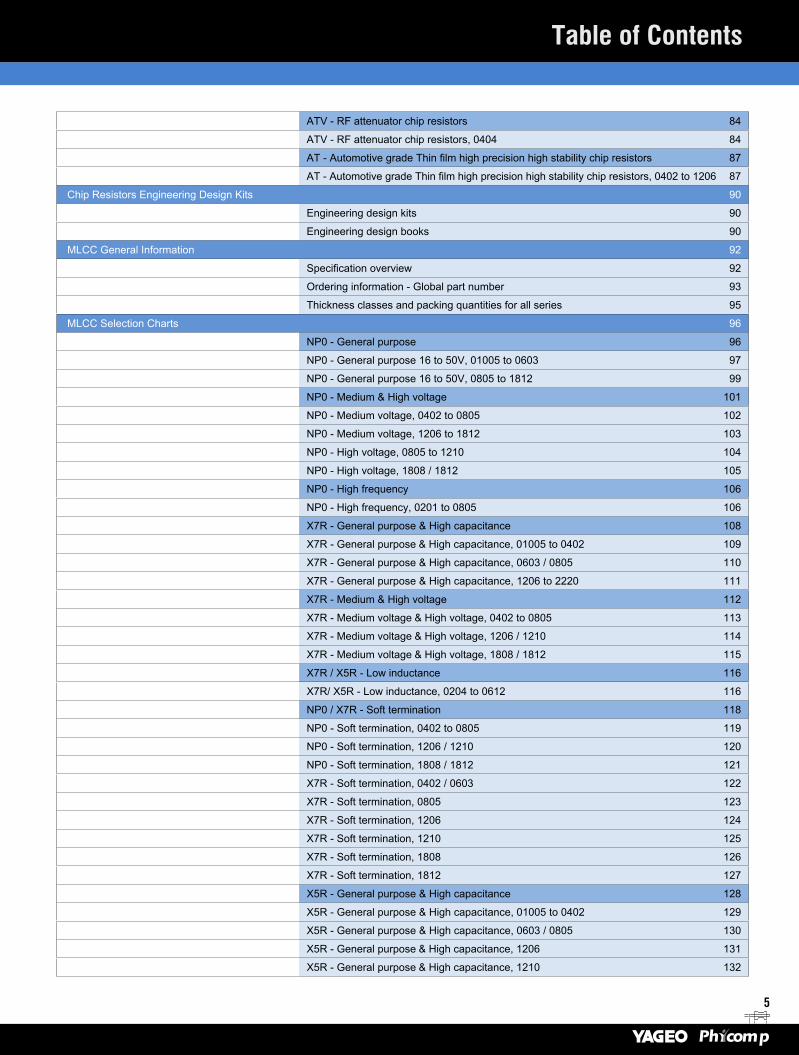
ATV - RF attenuator chip resistors 84
ATV - RF attenuator chip resistors, 0404 84
AT - Automotive grade Thin film high precision high stability chip resistors 87
AT - Automotive grade Thin film high precision high stability chip resistors, 0402 to 1206 87
Chip Resistors Engineering Design Kits 90
Engineering design kits 90
Engineering design books 90
MLCC General Information 92
Specification overview 92
Ordering information - Global part number 93
Thickness classes and packing quantities for all series 95
MLCC Selection Charts 96
NP0 - General purpose 96
NP0 - General purpose 16 to 50V, 01005 to 0603 97
NP0 - General purpose 16 to 50V, 0805 to 1812 99
NP0 - Medium & High voltage 101
NP0 - Medium voltage, 0402 to 0805 102
NP0 - Medium voltage, 1206 to 1812 103
NP0 - High voltage, 0805 to 1210 104
NP0 - High voltage, 1808 / 1812 105
NP0 - High frequency 106
NP0 - High frequency, 0201 to 0805 106
X7R - General purpose & High capacitance 108
X7R - General purpose & High capacitance, 01005 to 0402 109
X7R - General purpose & High capacitance, 0603 / 0805 110
X7R - General purpose & High capacitance, 1206 to 2220 111
X7R - Medium & High voltage 112
X7R - Medium voltage & High voltage, 0402 to 0805 113
X7R - Medium voltage & High voltage, 1206 / 1210 114
X7R - Medium voltage & High voltage, 1808 / 1812 115
X7R / X5R - Low inductance 116
X7R/ X5R - Low inductance, 0204 to 0612 116
NP0 / X7R - Soft termination 118
NP0 - Soft termination, 0402 to 0805 119
NP0 - Soft termination, 1206 / 1210 120
NP0 - Soft termination, 1808 / 1812 121
X7R - Soft termination, 0402 / 0603 122
X7R - Soft termination, 0805 123
X7R - Soft termination, 1206 124
X7R - Soft termination, 1210 125
X7R - Soft termination, 1808 126
X7R - Soft termination, 1812 127
X5R - General purpose & High capacitance 128
X5R - General purpose & High capacitance, 01005 to 0402 129
X5R - General purpose & High capacitance, 0603 / 0805 130
X5R - General purpose & High capacitance, 1206 131
X5R - General purpose & High capacitance, 1210 132
6
Table of Contents
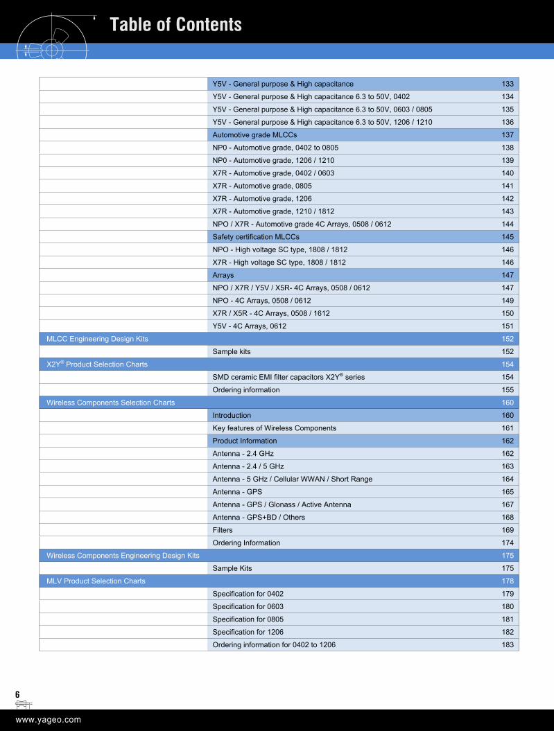
Y5V - General purpose & High capacitance 133
Y5V - General purpose & High capacitance 6.3 to 50V, 0402 134
Y5V - General purpose & High capacitance 6.3 to 50V, 0603 / 0805 135
Y5V - General purpose & High capacitance 6.3 to 50V, 1206 / 1210 136
Automotive grade MLCCs 137
NP0 - Automotive grade, 0402 to 0805 138
NP0 - Automotive grade, 1206 / 1210 139
X7R - Automotive grade, 0402 / 0603 140
X7R - Automotive grade, 0805 141
X7R - Automotive grade, 1206 142
X7R - Automotive grade, 1210 / 1812 143
NPO / X7R - Automotive grade 4C Arrays, 0508 / 0612 144
Safety certification MLCCs 145
NPO - High voltage SC type, 1808 / 1812 146
X7R - High voltage SC type, 1808 / 1812 146
Arrays 147
NPO / X7R / Y5V / X5R- 4C Arrays, 0508 / 0612 147
NPO - 4C Arrays, 0508 / 0612 149
X7R / X5R - 4C Arrays, 0508 / 1612 150
Y5V - 4C Arrays, 0612 151
MLCC Engineering Design Kits 152
Sample kits 152
X2Y® Product Selection Charts 154
SMD ceramic EMI filter capacitors X2Y® series 154
Ordering information 155
Wireless Components Selection Charts 160
Introduction 160
Key features of Wireless Components 161
Product Information 162
Antenna - 2.4 GHz 162
Antenna - 2.4 / 5 GHz 163
Antenna - 5 GHz / Cellular WWAN / Short Range 164
Antenna - GPS 165
Antenna - GPS / Glonass / Active Antenna 167
Antenna - GPS+BD / Others 168
Filters 169
Ordering Information 174
Wireless Components Engineering Design Kits 175
Sample Kits 175
MLV Product Selection Charts 178
Specification for 0402 179
Specification for 0603 180
Specification for 0805 181
Specification for 1206 182
Ordering information for 0402 to 1206 183
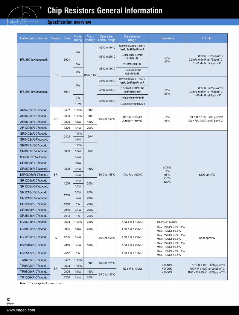
SURFACE-MOUNT CHIP RESISTORS
8
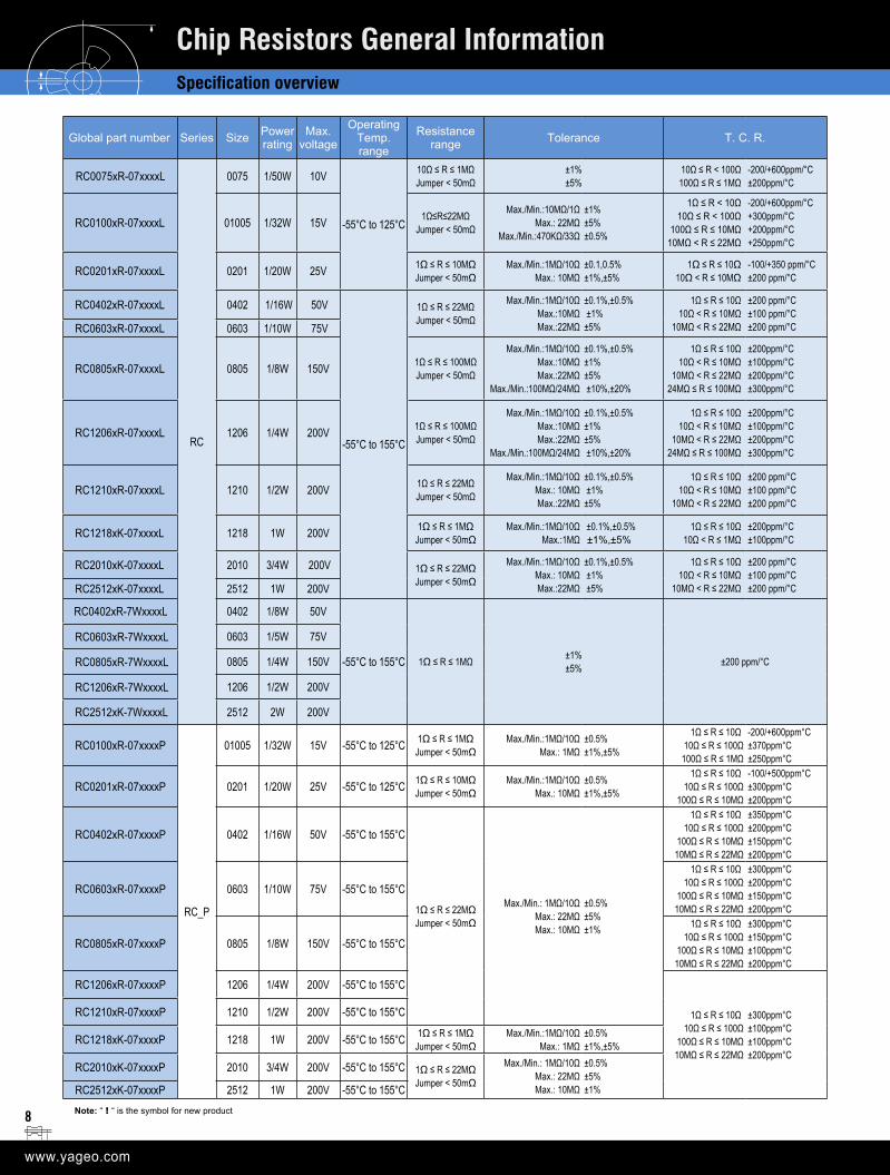
Chip Resistors General InformationSpecification overview
Global part number Series Size Power rating
Max. voltage
Operating Temp. range
Resistance range Tolerance T. C. R.
RC0075xR-07xxxxL
RC
0075 1/50W 10V
-55°C to 125°C
10Ω ≤ R ≤ 1MΩ Jumper < 50mΩ
±1%±5%
10Ω ≤ R < 100Ω100Ω ≤ R ≤ 1MΩ
-200/+600ppm/°C±200ppm/°C
RC0100xR-07xxxxL 01005 1/32W 15V 1Ω≤R≤22MΩJumper < 50mΩ
Max./Min.:10MΩ/1Ω Max.: 22MΩ
Max./Min.:470KΩ/33Ω
±1%±5%±0.5%
1Ω ≤ R < 10Ω 10Ω ≤ R < 100Ω
100Ω ≤ R ≤ 10MΩ10MΩ < R ≤ 22MΩ
-200/+600ppm/°C+300ppm/°C+200ppm/°C+250ppm/°C
RC0201xR-07xxxxL 0201 1/20W 25V 1Ω ≤ R ≤ 10MΩ Jumper < 50mΩ
Max./Min.:1MΩ/10Ω Max.: 10MΩ
±0.1,0.5%±1%,±5%
1Ω ≤ R ≤ 10Ω 10Ω < R ≤ 10MΩ
-100/+350 ppm/°C ±200 ppm/°C
RC0402xR-07xxxxL 0402 1/16W 50V
-55°C to 155°C
1Ω ≤ R ≤ 22MΩJumper < 50mΩ
Max./Min.:1MΩ/10Ω Max.:10MΩ Max.:22MΩ
±0.1%,±0.5% ±1%±5%
1Ω ≤ R ≤ 10Ω10Ω < R ≤ 10MΩ
10MΩ < R ≤ 22MΩ
±200 ppm/°C±100 ppm/°C±200 ppm/°C RC0603xR-07xxxxL 0603 1/10W 75V
RC0805xR-07xxxxL 0805 1/8W 150V 1Ω ≤ R ≤ 100MΩJumper < 50mΩ
Max./Min.:1MΩ/10Ω Max.:10MΩ Max.:22MΩ
Max./Min.:100MΩ/24MΩ
±0.1%,±0.5%±1%±5% ±10%,±20%
1Ω ≤ R ≤ 10Ω10Ω < R ≤ 10MΩ
10MΩ < R ≤ 22MΩ24MΩ ≤ R ≤ 100MΩ
±200ppm/°C±100ppm/°C±200ppm/°C±300ppm/°C
RC1206xR-07xxxxL 1206 1/4W 200V 1Ω ≤ R ≤ 100MΩJumper < 50mΩ
Max./Min.:1MΩ/10Ω Max.:10MΩ Max.:22MΩ
Max./Min.:100MΩ/24MΩ
±0.1%,±0.5%±1%±5% ±10%,±20%
1Ω ≤ R ≤ 10Ω10Ω < R ≤ 10MΩ
10MΩ < R ≤ 22MΩ24MΩ ≤ R ≤ 100MΩ
±200ppm/°C±100ppm/°C±200ppm/°C±300ppm/°C
RC1210xR-07xxxxL 1210 1/2W 200V 1Ω ≤ R ≤ 22MΩJumper < 50mΩ
Max./Min.:1MΩ/10Ω Max.: 10MΩMax.:22MΩ
±0.1%,±0.5% ±1%±5%
1Ω ≤ R ≤ 10Ω10Ω < R ≤ 10MΩ
10MΩ < R ≤ 22MΩ
±200 ppm/°C±100 ppm/°C±200 ppm/°C
RC1218xK-07xxxxL 1218 1W 200V 1Ω ≤ R ≤ 1MΩJumper < 50mΩ
Max./Min.:1MΩ/10ΩMax.:1MΩ
±0.1%,±0.5% ±1%,±5%
1Ω ≤ R ≤ 10Ω10Ω < R ≤ 1MΩ
±200ppm/°C±100ppm/°C
RC2010xK-07xxxxL 2010 3/4W 200V 1Ω ≤ R ≤ 22MΩJumper < 50mΩ
Max./Min.:1MΩ/10Ω Max.: 10MΩMax.:22MΩ
±0.1%,±0.5% ±1% ±5%
1Ω ≤ R ≤ 10Ω10Ω < R ≤ 10MΩ
10MΩ < R ≤ 22MΩ
±200 ppm/°C±100 ppm/°C±200 ppm/°C RC2512xK-07xxxxL 2512 1W 200V
RC0402xR-7WxxxxL 0402 1/8W 50V
-55°C to 155°C 1Ω ≤ R ≤ 1MΩ ±1%±5% ±200 ppm/°C
RC0603xR-7WxxxxL 0603 1/5W 75V
RC0805xR-7WxxxxL 0805 1/4W 150V
RC1206xR-7WxxxxL 1206 1/2W 200V
RC2512xK-7WxxxxL 2512 2W 200V
RC0100xR-07xxxxP
RC_P
01005 1/32W 15V -55°C to 125°C 1Ω ≤ R ≤ 1MΩJumper < 50mΩ
Max./Min.:1MΩ/10Ω Max.: 1MΩ
±0.5%±1%,±5%
1Ω ≤ R ≤ 10Ω10Ω ≤ R ≤ 100Ω100Ω ≤ R ≤ 1MΩ
-200/+600ppm°C±370ppm°C±250ppm°C
RC0201xR-07xxxxP 0201 1/20W 25V -55°C to 125°C 1Ω ≤ R ≤ 10MΩ Jumper < 50mΩ
Max./Min.:1MΩ/10Ω Max.: 10MΩ
±0.5%±1%,±5%
1Ω ≤ R ≤ 10Ω10Ω ≤ R ≤ 100Ω
100Ω ≤ R ≤ 10MΩ
-100/+500ppm°C±300ppm°C±200ppm°C
RC0402xR-07xxxxP 0402 1/16W 50V -55°C to 155°C
1Ω ≤ R ≤ 22MΩJumper < 50mΩ
Max./Min.: 1MΩ/10Ω Max.: 22MΩ
Max.: 10MΩ
±0.5%±5%±1%
1Ω ≤ R ≤ 10Ω10Ω ≤ R ≤ 100Ω
100Ω ≤ R ≤ 10MΩ10MΩ ≤ R ≤ 22MΩ
±350ppm°C±200ppm°C±150ppm°C±200ppm°C
RC0603xR-07xxxxP 0603 1/10W 75V -55°C to 155°C
1Ω ≤ R ≤ 10Ω10Ω ≤ R ≤ 100Ω
100Ω ≤ R ≤ 10MΩ10MΩ ≤ R ≤ 22MΩ
±300ppm°C±200ppm°C±150ppm°C±200ppm°C
RC0805xR-07xxxxP 0805 1/8W 150V -55°C to 155°C
1Ω ≤ R ≤ 10Ω10Ω ≤ R ≤ 100Ω
100Ω ≤ R ≤ 10MΩ10MΩ ≤ R ≤ 22MΩ
±300ppm°C±150ppm°C±100ppm°C±200ppm°C
RC1206xR-07xxxxP 1206 1/4W 200V -55°C to 155°C
1Ω ≤ R ≤ 10Ω10Ω ≤ R ≤ 100Ω
100Ω ≤ R ≤ 10MΩ10MΩ ≤ R ≤ 22MΩ
±300ppm°C±100ppm°C±100ppm°C±200ppm°C
RC1210xR-07xxxxP 1210 1/2W 200V -55°C to 155°C
RC1218xK-07xxxxP 1218 1W 200V -55°C to 155°C 1Ω ≤ R ≤ 1MΩJumper < 50mΩ
Max./Min.:1MΩ/10Ω Max.: 1MΩ
±0.5%±1%,±5%
RC2010xK-07xxxxP 2010 3/4W 200V -55°C to 155°C 1Ω ≤ R ≤ 22MΩJumper < 50mΩ
Max./Min.: 1MΩ/10Ω Max.: 22MΩ
Max.: 10MΩ
±0.5%±5%±1% RC2512xK-07xxxxP 2512 1W 200V -55°C to 155°C
Note: “ ! “ is the symbol for new product
9
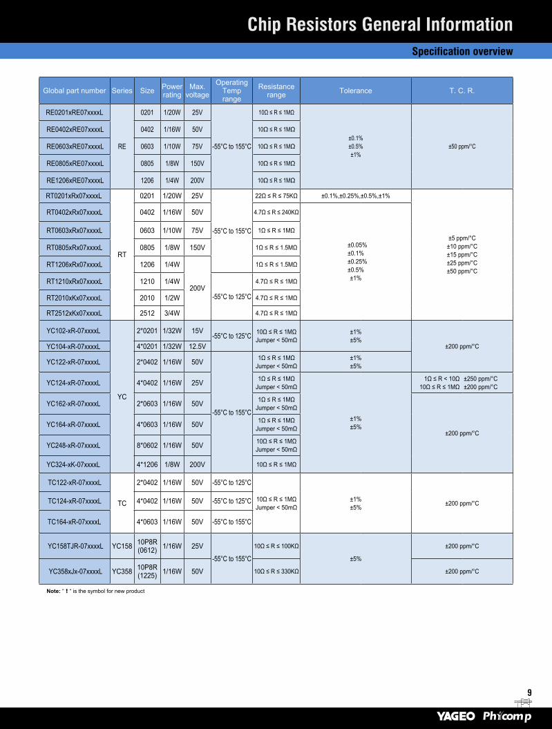
Chip Resistors General InformationSpecification overview
Global part number Series Size Power rating
Max. voltage
Operating Temp range
Resistance range Tolerance T. C. R.
RE0201xRE07xxxxL
RE
0201 1/20W 25V
-55°C to 155°C
10Ω ≤ R ≤ 1MΩ
±0.1%±0.5% ±1%
±50 ppm/°C
RE0402xRE07xxxxL 0402 1/16W 50V 10Ω ≤ R ≤ 1MΩ
RE0603xRE07xxxxL 0603 1/10W 75V 10Ω ≤ R ≤ 1MΩ
RE0805xRE07xxxxL 0805 1/8W 150V 10Ω ≤ R ≤ 1MΩ
RE1206xRE07xxxxL 1206 1/4W 200V 10Ω ≤ R ≤ 1MΩ
RT0201xRx07xxxxL
RT
0201 1/20W 25V
-55°C to 155°C
22Ω ≤ R ≤ 75KΩ ±0.1%,±0.25%,±0.5%,±1%
±5 ppm/°C ±10 ppm/°C ±15 ppm/°C ±25 ppm/°C ±50 ppm/°C
RT0402xRx07xxxxL 0402 1/16W 50V 4.7Ω ≤ R ≤ 240KΩ
±0.05%±0.1%
±0.25%±0.5%±1%
RT0603xRx07xxxxL 0603 1/10W 75V 1Ω ≤ R ≤ 1MΩ
RT0805xRx07xxxxL 0805 1/8W 150V 1Ω ≤ R ≤ 1.5MΩ
RT1206xRx07xxxxL 1206 1/4W
200V
1Ω ≤ R ≤ 1.5MΩ
RT1210xRx07xxxxL 1210 1/4W
-55°C to 125°C
4.7Ω ≤ R ≤ 1MΩ
RT2010xKx07xxxxL 2010 1/2W 4.7Ω ≤ R ≤ 1MΩ
RT2512xKx07xxxxL 2512 3/4W 4.7Ω ≤ R ≤ 1MΩ
YC102-xR-07xxxxL
YC
2*0201 1/32W 15V -55°C to 125°C 10Ω ≤ R ≤ 1MΩ
Jumper < 50mΩ±1%±5%
±200 ppm/°C YC104-xR-07xxxxL 4*0201 1/32W 12.5V
YC122-xR-07xxxxL 2*0402 1/16W 50V
-55°C to 155°C
1Ω ≤ R ≤ 1MΩJumper < 50mΩ
±1%±5%
YC124-xR-07xxxxL 4*0402 1/16W 25V 1Ω ≤ R ≤ 1MΩJumper < 50mΩ
±1%±5%
1Ω ≤ R < 10Ω10Ω ≤ R ≤ 1MΩ
±250 ppm/°C±200 ppm/°C
YC162-xR-07xxxxL 2*0603 1/16W 50V 1Ω ≤ R ≤ 1MΩJumper < 50mΩ
±200 ppm/°C YC164-xR-07xxxxL 4*0603 1/16W 50V 1Ω ≤ R ≤ 1MΩ
Jumper < 50mΩ
YC248-xR-07xxxxL 8*0602 1/16W 50V 10Ω ≤ R ≤ 1MΩJumper < 50mΩ
YC324-xK-07xxxxL 4*1206 1/8W 200V 10Ω ≤ R ≤ 1MΩ
TC122-xR-07xxxxL
TC
2*0402 1/16W 50V -55°C to 125°C
10Ω ≤ R ≤ 1MΩJumper < 50mΩ
±1% ±5% ±200 ppm/°CTC124-xR-07xxxxL 4*0402 1/16W 50V -55°C to 125°C
TC164-xR-07xxxxL 4*0603 1/16W 50V -55°C to 155°C
YC158TJR-07xxxxL YC158 10P8R (0612) 1/16W 25V
-55°C to 155°C
10Ω ≤ R ≤ 100KΩ
±5%
±200 ppm/°C
YC358xJx-07xxxxL YC358 10P8R (1225) 1/16W 50V 10Ω ≤ R ≤ 330KΩ ±200 ppm/°C
Note: “ ! “ is the symbol for new product
10
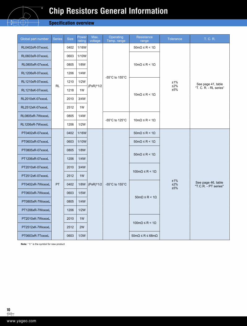
Chip Resistors General InformationSpecification overview
Global part number Series Size Power rating
Max. voltage
Operating Temp. range
Resistance range Tolerance T. C. R.
RL0402xR-07xxxxL
RL
0402 1/16W
(PxR)^1/2
-55°C to 155°C
50mΩ ≤ R < 1Ω
±1% ±2% ±5%
See page 41, table “T. C. R. - RL series“
RL0603xR-07xxxxL 0603 1/10W
10mΩ ≤ R < 1Ω RL0805xR-07xxxxL 0805 1/8W
RL1206xR-07xxxxL 1206 1/4W
RL1210xR-07xxxxL 1210 1/2W
10mΩ ≤ R < 1Ω RL1218xK-07xxxxL 1218 1W
RL2010xK-07xxxxL 2010 3/4W
RL2512xK-07xxxxL 2512 1W
RL0805xR-7WxxxxL 0805 1/4W -55°C to 125°C 10mΩ ≤ R < 1Ω
RL1206xR-7WxxxxL 1206 1/2W
PT0402xR-07xxxxL
PT
0402 1/16W
(PxR)^1/2 -55°C to 155°C
50mΩ ≤ R < 1Ω
±1% ±2% ±5%
See page 46, table "T.C.R. - PT series"
PT0603xR-07xxxxL 0603 1/10W 50mΩ ≤ R < 1Ω
PT0805xR-07xxxxL 0805 1/8W50mΩ ≤ R < 1Ω
PT1206xR-07xxxxL 1206 1/4W
PT2010xK-07xxxxL 2010 3/4W 100mΩ ≤ R < 1Ω
PT2512xK-07xxxxL 2512 1W
PT0402xR-7WxxxxL 0402 1/8W
50mΩ ≤ R < 1Ω PT0603xR-7WxxxxL 0603 1/5W
PT0805xR-7WxxxxL 0805 1/4W
PT1206xR-7WxxxxL 1206 1/2W
PT2010xK-7WxxxxL 2010 1W100mΩ ≤ R < 1Ω
PT2512xK-7WxxxxL 2512 2W
PT0603xR-7TxxxxL 0603 1/3W 50mΩ ≤ R ≤ 68mΩ
Note: “ ! “ is the symbol for new product
11
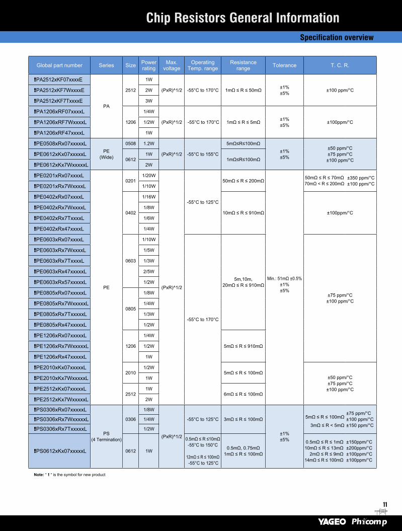
Global part number Series Size Power rating
Max. voltage
Operating Temp. range
Resistance range Tolerance T. C. R.
!PA2512xKF07xxxxE
PA
2512
1W
(PxR)^1/2 -55°C to 170°C 1mΩ ≤ R ≤ 50mΩ ±1% ±5% ±100 ppm/°C !PA2512xKF7WxxxxE 2W
!PA2512xKF7TxxxxE 3W
!PA1206xRF07xxxxL
1206
1/4W
(PxR)^1/2 -55°C to 170°C 1mΩ ≤ R ≤ 5mΩ ±1%±5% ±100ppm/°C !PA1206xRF7WxxxxL 1/2W
!PA1206xRF47xxxxL 1W
!PE0508xRx07xxxxxLPE
(Wide)
0508 1.2W
(PxR)^1/2 -55°C to 155°C
5mΩ≤R≤100mΩ±1%±5%
±50 ppm/°C±75 ppm/°C
±100 ppm/°C !PE0612xKx07xxxxxL
06121W
1mΩ≤R≤100mΩ !PE0612xKx7WxxxxxL 2W
!PE0201xRx07xxxxL
PE
02011/20W
(PxR)^1/2
-55°C to 125°C
50mΩ ≤ R ≤ 200mΩ
Min.: 51mΩ ±0.5% ±1% ±5%
50mΩ ≤ R ≤ 70mΩ 70mΩ < R ≤ 200mΩ
±350 ppm/°C±100 ppm/°C !PE0201xRx7WxxxxL 1/10W
!PE0402xRx07xxxxL
0402
1/16W
10mΩ ≤ R ≤ 910mΩ ±100ppm/°C !PE0402xRx7WxxxxL 1/8W
!PE0402xRx7TxxxxL 1/6W
!PE0402xRx47xxxxL 1/4W
!PE0603xRx07xxxxL
0603
1/10W
-55°C to 170°C
5m,10m,20mΩ ≤ R ≤ 910mΩ
±75 ppm/°C±100 ppm/°C
!PE0603xRx7WxxxxL 1/5W
!PE0603xRx7TxxxxL 1/3W
!PE0603xRx47xxxxxL 2/5W
!PE0603xRx57xxxxxL 1/2W
!PE0805xRx07xxxxxL
0805
1/8W
!PE0805xRx7WxxxxxL 1/4W
!PE0805xRx7TxxxxxL 1/3W
!PE0805xRx47xxxxxL 1/2W
!PE1206xRx07xxxxxL
1206
1/4W
5mΩ ≤ R ≤ 910mΩ !PE1206xRx7WxxxxxL 1/2W
!PE1206xRx47xxxxxL 1W
!PE2010xKx07xxxxxL2010
1/2W5mΩ ≤ R ≤ 100mΩ
±50 ppm/°C±75 ppm/°C
±100 ppm/°C
!PE2010xKx7WxxxxxL 1W
!PE2512xKx07xxxxxL2512
1W6mΩ ≤ R ≤ 100mΩ
!PE2512xKx7WxxxxxL 2W
!PS0306xRx07xxxxxL
PS(4 Termination)
0306
1/8W
(PxR)^1/2
-55°C to 125°C 3mΩ ≤ R ≤ 100mΩ
±1%±5%
3mΩ ≤ R < 5mΩ
±75 ppm/°C±100 ppm/°C±150 ppm/°C
!PS0306xRx7WxxxxxL 1/4W
!PS0306xRx7TxxxxxL 1/2W
!PS0612xKx07xxxxxL 0612 1W
0.5mΩ ≤ R ≤10mΩ -55°C to 150°C
12mΩ ≤ R ≤ 100mΩ -55°C to 125°C
0.5mΩ, 0.75mΩ1mΩ ≤ R ≤ 100mΩ
0.5mΩ ≤ R ≤ 1mΩ10mΩ ≤ R ≤ 13mΩ
2mΩ ≤ R ≤ 9mΩ14mΩ ≤ R ≤ 100mΩ
±150ppm/°C±200ppm/°C±100ppm/°C±100ppm/°C
Note: “ ! “ is the symbol for new product
Chip Resistors General InformationSpecification overview
5mΩ ≤ R ≤ 100mΩ
12
Chip Resistors General InformationSpecification overview
Global part number Series Size Power rating
Max. voltage
Operating Temp. range
Resistance range Tolerance T. C. R.
!PU3921xKxxxxxxxL
PU
3921
3W
(PxR)^1/2
-55°C to 170°C 0.2mR/ 0.3mR/ 0.5mR/ 1mR/ 2mR/3mR/4mR
±1%±5%
0.2mR0.3mR/ 0.5mR
1mR~4mR
±325ppm/°C±175ppm/°C±75ppm/°C
-55°C to 275°C 0.5mR/1mR/ 2mR/3mR/4mR
5W -55°C to 170°C
2mR/3mR/4mR
9W 0.2mR/ 0.3mR/ 0.5mR/1mR
!PU5931xKxxxxxxxL 5931
5W -55°C to 170°C 0.2mR/ 0.3mR/ 0.5mR/
1mR/ 2mR/3mR/4mR
±1%±5%
0.2mR0.3mR/ 0.5mR
1mR~4mR
±225ppm/°C±175ppm/°C±75ppm/°C
-55°C to 275°C 0.3mR/ 0.5mR/1mR/ 2mR/3mR/4mR
7W -55°C to 170°C
1mR/2mR/3mR/4mR
10W 0.2mR/ 0.3mR/ 0.5mR
AR0402xR-07xxxxL
AR
0402 1/16W 50V
-55°C to 155°C 1Ω ≤ R ≤ 10MΩJumper < 50mΩ
±1% ±5%
1Ω ≤ R ≤ 10Ω10Ω < R ≤ 10MΩ
±200 ppm/°C±100 ppm/°C
AR0603xR-07xxxxL 0603 1/10W 50V
AR0805xR-07xxxxL 0805 1/8W 150V
AR1206xR-07xxxxL 1206 1/4W 200V
SR0402xR-07xxxxL
SR
04021/16W
50V
-55°C to 155°C 1Ω ≤ R ≤ 100KΩ
±0.5%±1%±5%
±10% ±20%
±200 ppm/°C
SR0402xR-7WxxxxL 1/8W
SR0603xR-07xxxxL
0603
1/10W
75V SR0603xR-7WxxxxL 1/5W
!SR0603xR-7TxxxxL 1/4W
SR0805xR-07xxxxL
0805
1/8W
150V SR0805xR-7WxxxxL 1/4W
!SR0805xR-7TxxxxL 1/3W
SR1206xR-07xxxxL 1206
1/4W 200V
SR1206xR-7WxxxxL 1/2W
SR1210xR-07xxxxL1210
1/2W 200V
SR1210xR-7WxxxxL 3/4W 200V
SR1218xK-07xxxxL 1218 1W 200V
SR2010xK-07xxxxL 2010 3/4W 200V
SR2512xK-07xxxxL 2512 1W 200V
RV0603xR-07xxxxL
RV
0603 1/10W 350V
-55°C to 155°C
47Ω ≤ R ≤ 10MΩ ±0.5%,±1%,±5%
±200 ppm/°C
RV0805xR-07xxxxL 0805 1/8W 400V 47Ω ≤ R ≤ 22MΩ Max.: 22MΩMax.: 10MΩ
±5%,±1%±0.5%
RV1206xR-07xxxxL 1206 1/4W
500V
47Ω ≤ R ≤ 27MΩ Max.: 27MΩMax.: 10MΩ
±5%,±1%±0.5%
RV2010xK-07xxxxL 2010 3/4W 47Ω ≤ R ≤ 22MΩ Max.: 22MΩMax.: 10MΩ
±5%,±1%±0.5%
RV2512xK-07xxxxL 2512 1W 47Ω ≤ R ≤ 16MΩ Max.: 16MΩMax.: 10MΩ
±5%,±1%±0.5%
TR0402xR-07xxxxL
TR
0402 1/16W 50V -55°C to 125°C
1Ω ≤ R ≤ 10MΩ +0/-10% +0/-20% +0/-30%
1Ω ≤ R ≤ 10Ω 10Ω < R ≤ 1MΩ
1MΩ < R ≤ 10MΩ
±200 ppm/°C ±100 ppm/°C ±200 ppm/°C
TR0603xR-07xxxxL 0603 1/16W
TR0805xR-07xxxxL 0805 1/8W 150V -55°C to 155°C
TR1206xR-07xxxxL 1206 1/4W 200V
Note: “ ! “ is the symbol for new product
13
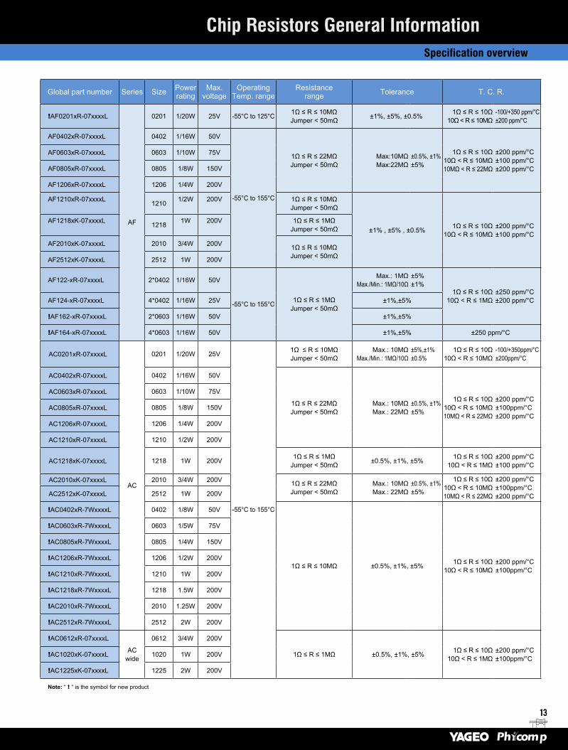
Chip Resistors General InformationSpecification overview
Global part number Series Size Power rating
Max. voltage
Operating Temp. range
Resistance range Tolerance T. C. R.
!AF0201xR-07xxxxL
AF
0201 1/20W 25V -55°C to 125°C 1Ω ≤ R ≤ 10MΩJumper < 50mΩ ±1%, ±5%, ±0.5% 1Ω ≤ R ≤ 10Ω
10Ω < R ≤ 10MΩ-100/+350 ppm/°C±200 ppm/°C
AF0402xR-07xxxxL 0402 1/16W 50V
-55°C to 155°C
1Ω ≤ R ≤ 22MΩJumper < 50mΩ
Max:10MΩMax:22MΩ
±0.5%, ±1%±5%
1Ω ≤ R ≤ 10Ω10Ω < R ≤ 10MΩ10MΩ < R ≤ 22MΩ
±200 ppm/°C±100 ppm/°C±200 ppm/°C
AF0603xR-07xxxxL 0603 1/10W 75V
AF0805xR-07xxxxL 0805 1/8W 150V
AF1206xR-07xxxxL 1206 1/4W 200V
AF1210xR-07xxxxL 1210 1/2W 200V 1Ω ≤ R ≤ 10MΩ Jumper < 50mΩ
±1% , ±5% , ±0.5% 1Ω ≤ R ≤ 10Ω10Ω < R ≤ 10MΩ
±200 ppm/°C±100 ppm/°C
AF1218xK-07xxxxL 1218 1W 200V 1Ω ≤ R ≤ 1MΩ Jumper < 50mΩ
AF2010xK-07xxxxL 2010 3/4W 200V 1Ω ≤ R ≤ 10MΩ Jumper < 50mΩ AF2512xK-07xxxxL 2512 1W 200V
AF122-xR-07xxxxL 2*0402 1/16W 50V
-55°C to 155°C 1Ω ≤ R ≤ 1MΩJumper < 50mΩ
Max.: 1MΩMax./Min.: 1MΩ/10Ω
±5%±1%
1Ω ≤ R ≤ 10Ω 10Ω < R ≤ 1MΩ
±250 ppm/°C±200 ppm/°C AF124-xR-07xxxxL 4*0402 1/16W 25V ±1%,±5%
!AF162-xR-07xxxxL 2*0603 1/16W 50V ±1%,±5%
!AF164-xR-07xxxxL 4*0603 1/16W 50V ±1%,±5% ±250 ppm/°C
AC0201xR-07xxxxL
AC
0201 1/20W 25V
-55°C to 155°C
1Ω ≤ R ≤ 10MΩJumper < 50mΩ
Max.: 10MΩMax./Min.: 1MΩ/10Ω
±5%,±1%±0.5%
1Ω ≤ R ≤ 10Ω10Ω < R ≤ 10MΩ
-100/+350ppm/°C±200ppm/°C
AC0402xR-07xxxxL 0402 1/16W 50V
1Ω ≤ R ≤ 22MΩJumper < 50mΩ
Max.: 10MΩMax.: 22MΩ
±0.5%, ±1%±5%
1Ω ≤ R ≤ 10Ω10Ω < R ≤ 10MΩ10MΩ < R ≤ 22MΩ
±200 ppm/°C±100ppm/°C±200 ppm/°C
AC0603xR-07xxxxL 0603 1/10W 75V
AC0805xR-07xxxxL 0805 1/8W 150V
AC1206xR-07xxxxL 1206 1/4W 200V
AC1210xR-07xxxxL 1210 1/2W 200V
AC1218xK-07xxxxL 1218 1W 200V 1Ω ≤ R ≤ 1MΩJumper < 50mΩ ±0.5%, ±1%, ±5% 1Ω ≤ R ≤ 10Ω
10Ω < R ≤ 1MΩ±200 ppm/°C±100 ppm/°C
AC2010xK-07xxxxL 2010 3/4W 200V 1Ω ≤ R ≤ 22MΩJumper < 50mΩ
Max.: 10MΩMax.: 22MΩ
±0.5%, ±1%±5%
1Ω ≤ R ≤ 10Ω10Ω < R ≤ 10MΩ10MΩ < R ≤ 22MΩ
±200 ppm/°C±100ppm/°C±200 ppm/°C AC2512xK-07xxxxL 2512 1W 200V
!AC0402xR-7WxxxxL 0402 1/8W 50V
1Ω ≤ R ≤ 10MΩ ±0.5%, ±1%, ±5% 1Ω ≤ R ≤ 10Ω10Ω < R ≤ 10MΩ
±200 ppm/°C±100ppm/°C
!AC0603xR-7WxxxxL 0603 1/5W 75V
!AC0805xR-7WxxxxL 0805 1/4W 150V
!AC1206xR-7WxxxxL 1206 1/2W 200V
!AC1210xR-7WxxxxL 1210 1W 200V
!AC1218xR-7WxxxxL 1218 1.5W 200V
!AC2010xR-7WxxxxL 2010 1.25W 200V
!AC2512xR-7WxxxxL 2512 2W 200V
!AC0612xR-07xxxxL
AC wide
0612 3/4W 200V
1Ω ≤ R ≤ 1MΩ ±0.5%, ±1%, ±5% 1Ω ≤ R ≤ 10Ω10Ω < R ≤ 1MΩ
±200 ppm/°C±100ppm/°C !AC1020xK-07xxxxL 1020 1W 200V
!AC1225xK-07xxxxL 1225 2W 200V
Note: “ ! “ is the symbol for new product
14
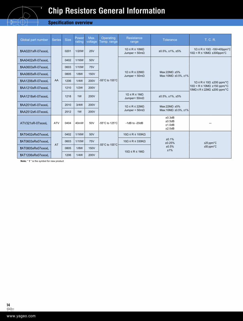
Chip Resistors General InformationSpecification overview
Global part number Series Size Power rating
Max. voltage
Operating Temp. range
Resistance range Tolerance T. C. R.
!AA0201xR-07xxxxL
AA
0201 1/20W 25V
-55°C to 155°C
1Ω ≤ R ≤ 10MΩJumper < 50mΩ ±0.5%, ±1%, ±5% 1Ω ≤ R ≤ 10Ω
10Ω < R ≤ 10MΩ-100/+400ppm/°C±300ppm°C
!AA0402xR-07xxxxL 0402 1/16W 50V
1Ω ≤ R ≤ 22MΩJumper < 50mΩ
Max:22MΩMax:10MΩ
±5%±0.5%, ±1%
1Ω ≤ R ≤ 10Ω10Ω < R ≤ 10MΩ10MΩ ≤ R ≤ 22MΩ
±200 ppm/°C±150 ppm/°C±200 ppm/°C
!AA0603xR-07xxxxL 0603 1/10W 75V
!AA0805xR-07xxxxL 0805 1/8W 150V
!AA1206xR-07xxxxL 1206 1/4W 200V
!AA1210xR-07xxxxL 1210 1/2W 200V
!AA1218xK-07xxxxL 1218 1W 200V 1Ω ≤ R ≤ 1MΩJumper< 50mΩ ±0.5%, ±1%, ±5%
!AA2010xK-07xxxxL 2010 3/4W 200V 1Ω ≤ R ≤ 22MΩJumper < 50mΩ
Max:22MΩMax:10MΩ
±5%±0.5%, ±1%
!AA2512xK-07xxxxL 2512 1W 200V
ATV321xR-07xxxxL ATV 0404 40mW 50V -55°C to 125°C -1dB to -20dB
±0.3dB ±0.5dB ±1.0dB ±2.0dB
---
!AT0402xRx07xxxxL
AT
0402 1/16W 50V
-55°C to 155°C
10Ω ≤ R ≤ 100KΩ
±0.1%±0.25%±0.5%±1%
±25 ppm/°C±50 ppm/°C
!AT0603xRx07xxxxL 0603 1/10W 75V 10Ω ≤ R ≤ 330KΩ
!AT0805xRx07xxxxL 0805 1/8W 150V10Ω ≤ R ≤ 1MΩ
!AT1206xRx07xxxxL 1206 1/4W 200V
Note: " ! " is the symbol for new product
15
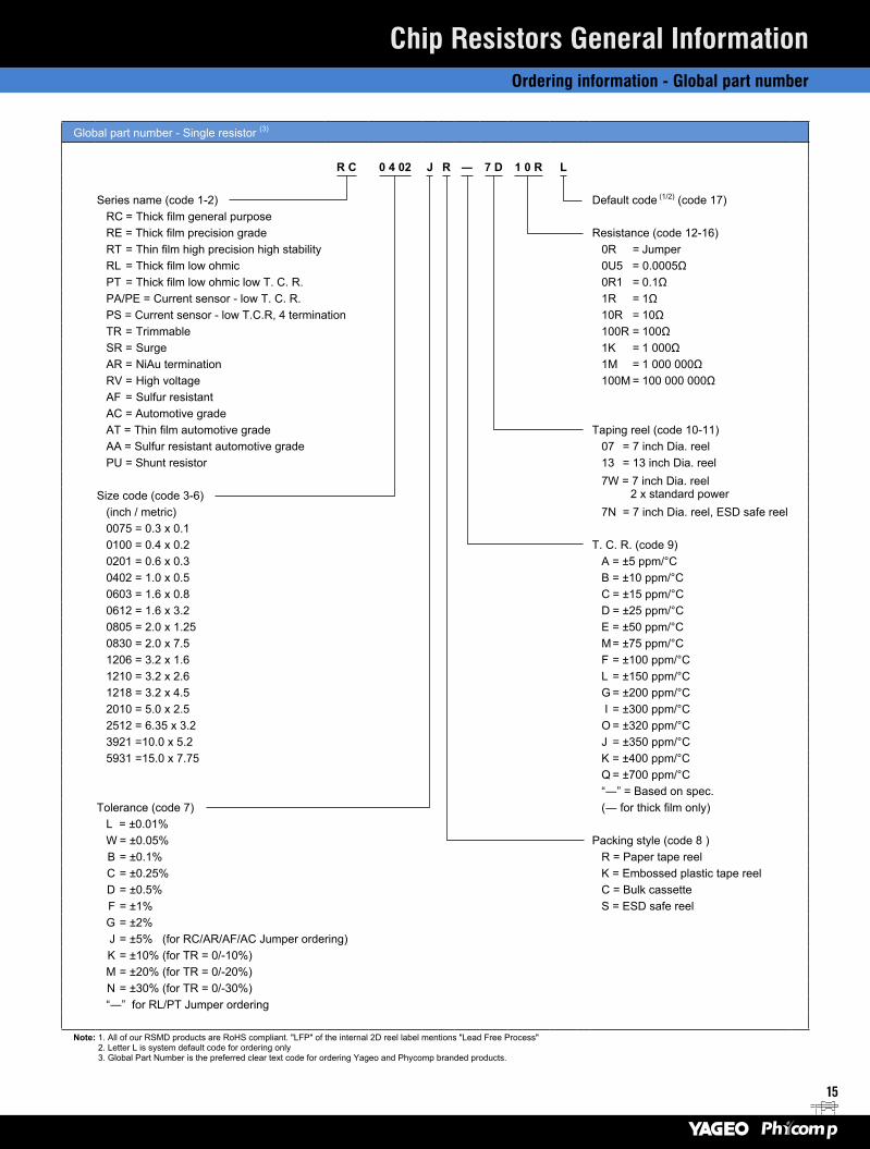
Global part number - Single resistor (3)
R C 0 4 02 J R ― 7 D 1 0 R L
Series name (code 1-2) Default code (1/2) (code 17) RC = Thick film general purposeRE = Thick film precision grade Resistance (code 12-16) RT = Thin film high precision high stability 0R = Jumper RL = Thick film low ohmic 0U5 = 0.0005ΩPT = Thick film low ohmic low T. C. R. 0R1 = 0.1ΩPA/PE = Current sensor - low T. C. R. 1R = 1ΩPS = Current sensor - low T.C.R, 4 termination 10R = 10ΩTR = Trimmable 100R = 100Ω SR = Surge 1K = 1 000ΩAR = NiAu termination 1M = 1 000 000Ω RV = High voltage 100M = 100 000 000ΩAF = Sulfur resistantAC = Automotive gradeAT = Thin film automotive grade Taping reel (code 10-11)AA = Sulfur resistant automotive grade 07 = 7 inch Dia. reelPU = Shunt resistor 13 = 13 inch Dia. reel
7W = 7 inch Dia. reel 2 x standard powerSize code (code 3-6)
(inch / metric) 7N = 7 inch Dia. reel, ESD safe reel0075 = 0.3 x 0.10100 = 0.4 x 0.2 T. C. R. (code 9)0201 = 0.6 x 0.3 A = ±5 ppm/°C 0402 = 1.0 x 0.5 B = ±10 ppm/°C 0603 = 1.6 x 0.8 C = ±15 ppm/°C 0612 = 1.6 x 3.2 D = ±25 ppm/°C0805 = 2.0 x 1.25 E = ±50 ppm/°C0830 = 2.0 x 7.5 M = ±75 ppm/°C1206 = 3.2 x 1.6 F = ±100 ppm/°C1210 = 3.2 x 2.6 L = ±150 ppm/°C 1218 = 3.2 x 4.5 G = ±200 ppm/°C2010 = 5.0 x 2.5 I = ±300 ppm/°C2512 = 6.35 x 3.2 O = ±320 ppm/°C3921 =10.0 x 5.2 J = ±350 ppm/°C5931 =15.0 x 7.75 K = ±400 ppm/°C
Q = ±700 ppm/°C“―” = Based on spec.
Tolerance (code 7) (― for thick film only)L = ±0.01% W = ±0.05% Packing style (code 8 ) B = ±0.1% R = Paper tape reel C = ±0.25% K = Embossed plastic tape reel D = ±0.5% C = Bulk cassette
F = ±1% S = ESD safe reel G = ±2% J = ±5% (for RC/AR/AF/AC Jumper ordering) K = ±10% (for TR = 0/-10%) M = ±20% (for TR = 0/-20%) N = ±30% (for TR = 0/-30%)“―” for RL/PT Jumper ordering
Note: 1. All of our RSMD products are RoHS compliant. "LFP" of the internal 2D reel label mentions "Lead Free Process" 2. Letter L is system default code for ordering only 3. Global Part Number is the preferred clear text code for ordering Yageo and Phycomp branded products.
Chip Resistors General InformationOrdering information - Global part number
16
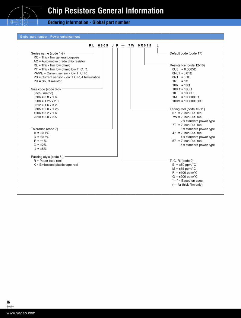
Global part number - Power enhancement
R L 0 8 0 5 J R ― 7 W 0 R 0 1 5 L
Series name (code 1-2) Default code (code 17) RC = Thick film general purposeAC = Automotive grade chip resistor RL = Thick film low ohmic Resistance (code 12-16)PT = Thick film low ohmic low T. C. R. 0U5 = 0.0005Ω PA/PE = Current sensor - low T. C. R. 0R01 = 0.01ΩPS = Current sensor - low T.C.R, 4 termination 0R1 = 0.1ΩPU = Shunt resistor 1R = 1Ω
10R = 10Ω Size code (code 3-6) 100R = 100Ω
(inch / metric) 1K = 1000Ω 0306 = 0.8 x 1.6 1M = 1000000Ω 0508 = 1.25 x 2.0 100M = 100000000Ω0612 = 1.6 x 3.20805 = 2.0 x 1.25 Taping reel (code 10-11)1206 = 3.2 x 1.6 07 = 7 inch Dia. reel2010 = 5.0 x 2.5 7W = 7 inch Dia. reel
2 x standard power type7T = 7 inch Dia. reel
Tolerance (code 7) 3 x standard power type B = ±0.1% 47 = 7 inch Dia. reel D = ±0.5% 4 x standard power type F = ±1% 57 = 7 inch Dia. reel G = ±2% 5 x standard power type J = ±5%
Packing style (code 8 )R = Paper tape reel T. C. R. (code 9)K = Embossed plastic tape reel E = ±50 ppm/°C
M = ±75 ppm/°CF = ±100 ppm/°C G = ±200 ppm/°C “―” = Based on spec.(― for thick film only)
Chip Resistors General InformationOrdering information - Global part number
17
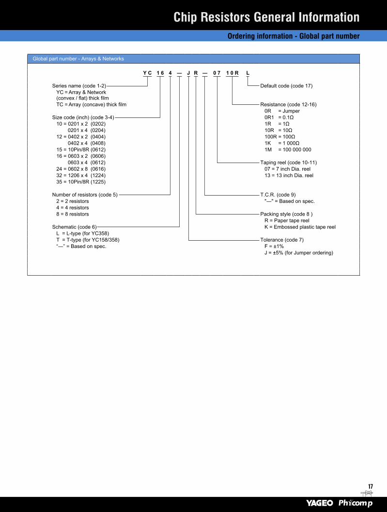
Global part number - Arrays & Networks
Y C 1 6 4 ― J R ― 0 7 1 0 R L
Series name (code 1-2) Default code (code 17) YC = Array & Network (convex / flat) thick filmTC = Array (concave) thick film Resistance (code 12-16)
0R = JumperSize code (inch) (code 3-4) 0R1 = 0.1Ω
10 = 0201 x 2 (0202) 1R = 1Ω 0201 x 4 (0204) 10R = 10Ω12 = 0402 x 2 (0404) 100R = 100Ω 0402 x 4 (0408) 1K = 1 000Ω15 = 10Pin/8R (0612) 1M = 100 000 00016 = 0603 x 2 (0606) 0603 x 4 (0612) Taping reel (code 10-11)24 = 0602 x 8 (0616) 07 = 7 inch Dia. reel32 = 1206 x 4 (1224) 13 = 13 inch Dia. reel35 = 10Pin/8R (1225)
Number of resistors (code 5) T.C.R. (code 9)2 = 2 resistors "―" = Based on spec.4 = 4 resistors8 = 8 resistors Packing style (code 8 )
R = Paper tape reelSchematic (code 6) K = Embossed plastic tape reel
L = L-type (for YC358)T = T-type (for YC158/358) Tolerance (code 7)“―” = Based on spec. F = ±1%
J = ±5% (for Jumper ordering)
Chip Resistors General InformationOrdering information - Global part number
18
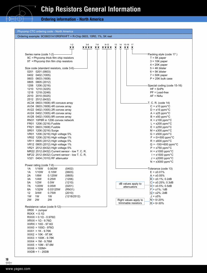
Phycomp CTC ordering code - North America
Ordering example: 9C06031A10R0FKHFT = R-Chip 0603, 10R0, 1%, 5K reel
1-2 3-6 7-8 9-12 13 14 15-16 17X X X X X X X X X X X X X X X X X
Series name (code 1-2) Packing style (code 17 ) 9C = Phycomp thick film chip resistors T = 5K paper 9T = Phycomp thin film chip resistors 3 = 10K paper
4 = 20K paperSize code (standard resistors, code 3-6) 5 = 4K blister
0201 0201 (0603) 6 = 5K blister0402 0402 (1005) 7 = 50K paper0603 0603 (1608) P = 25K bulk case0805 0805 (2012)1206 1206 (3216) Special coding (code 15-16)1210 1210 (3225) HF = SnPb1218 1218 (3248) PF = Lead-free2010 2010 (5025) AF = NiAu2512 2512 (6432)AC34 0603 (1608) 4R concave array T. C. R. (code 14)AV34 0603 (1608) 4R convex array C = ±10 ppm/°CAV22 0402 (1005) 2R convex array D = ±15 ppm/°CAV24 0402 (1005) 4R convex array A = ±25 ppm/°CAV28 0402 (1005) 8R convex array B = ±50 ppm/°CRN31 10P8R in 1206 convex network K = ±100 ppm/°CFR01 1206 (3216) Fusible L = ±200 ppm/°CFR21 0603 (1608) Fusible E = ±250 ppm/°CSR01 1206 (3216) Surge M = ±300 ppm/°CVR01 1206 (3216) High voltage 5% G = ±500 ppm/°CVR02 1206 (3216) High voltage 1% F = 0/+500 ppm/°CVR11 0805 (2012) High voltage 5% R = ±600 ppm/°CVR12 0805 (2012) High voltage 1% Q = -100/+600 ppm/°C
VR21 2512 (6432) High voltage 5% P = ±750 ppm/°CMR22 2512 (6432) Current sensor - low T. C. R. H = ±1000 ppm/°CMF22 2512 (6432) Current sensor - low T. C. R. I = ±1500 ppm/°CV321 0404 (1010) RF attenuator J = ±2000 ppm/°C
N = ±3000 ppm/°CPower rating (code 7-8)
1A 1/16W 0.063W (0402) Tolerance (code 13)1A 1/10W 0.10W (0603) E = ±0.01%2A 1/8W 0.125W (0805) A = ±0.05% 3A 1/4W 0.25W (1206) B = ±0.1%; 0.2dB5A 1/2W 0.5W (1210) C = ±0.25%; 0.3dB7A 1/20W 0.05W (0201) D = ±0.5%; 0.5dB8A 1/32W 0.03125W (RN31) F = ±1%; 1dB12 3/4W 0.75W (2010) G = ±2%; 2dB1W 1W 1W (1218/2512) J = ±5%2W 2W 2W N = 0/-20%
R = 0/-30%Resistance value (code 9-12)
0R00 = JumperR0XX < 0.1ΩRXXX = 0.1Ω - 0.976ΩXRXX = 1Ω - 9.76ΩXXRX = 10Ω - 97.6ΩXXX0 = 100Ω - 976ΩXXX1 = 1K - 9.76KXXX2 = 10K - 97.6KXXX3 = 100K - 9.78KXXX4 = 1M - 9.76MXXX5 = 10M - 97.6MXXX6 = 100M+XXDB = 1 - 20DB
Right values apply to trimmable resistors
dB values apply to attenuators
Chip Resistors General InformationOrdering information - North America
19
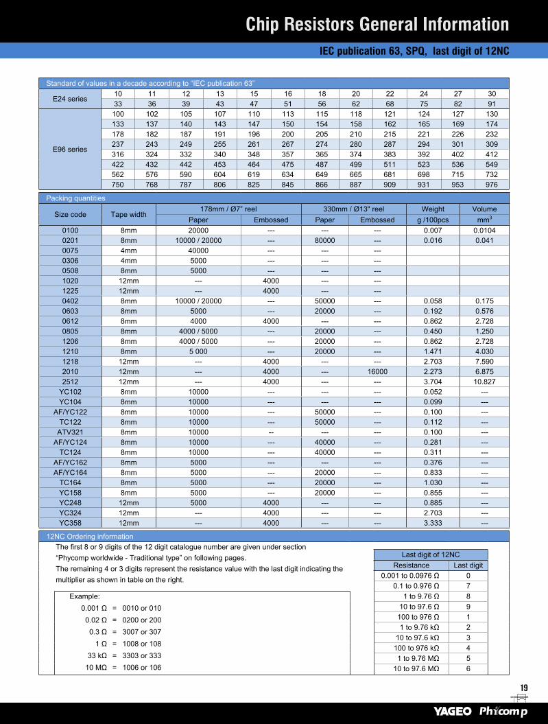
Standard of values in a decade according to “IEC publication 63”
E24 series10 11 12 13 15 16 18 20 22 24 27 3033 36 39 43 47 51 56 62 68 75 82 91
E96 series
100 102 105 107 110 113 115 118 121 124 127 130133 137 140 143 147 150 154 158 162 165 169 174178 182 187 191 196 200 205 210 215 221 226 232237 243 249 255 261 267 274 280 287 294 301 309316 324 332 340 348 357 365 374 383 392 402 412422 432 442 453 464 475 487 499 511 523 536 549562 576 590 604 619 634 649 665 681 698 715 732750 768 787 806 825 845 866 887 909 931 953 976
Packing quantities
Size code Tape width178mm / Ø7” reel 330mm / Ø13" reel Weight Volume
Paper Embossed Paper Embossed g /100pcs mm3
0100 8mm 20000 --- --- --- 0.007 0.01040201 8mm 10000 / 20000 --- 80000 --- 0.016 0.0410075 4mm 40000 --- --- ---0306 4mm 5000 --- --- ---0508 8mm 5000 --- --- ---1020 12mm --- 4000 --- ---1225 12mm --- 4000 --- ---0402 8mm 10000 / 20000 --- 50000 --- 0.058 0.1750603 8mm 5000 --- 20000 --- 0.192 0.5760612 8mm 4000 4000 --- --- 0.862 2.7280805 8mm 4000 / 5000 --- 20000 --- 0.450 1.2501206 8mm 4000 / 5000 --- 20000 --- 0.862 2.7281210 8mm 5 000 --- 20000 --- 1.471 4.0301218 12mm --- 4000 --- --- 2.703 7.5902010 12mm --- 4000 --- 16000 2.273 6.8752512 12mm --- 4000 --- --- 3.704 10.827
YC102 8mm 10000 --- --- --- 0.052 ---YC104 8mm 10000 --- --- --- 0.099 ---
AF/YC122 8mm 10000 --- 50000 --- 0.100 ---TC122 8mm 10000 --- 50000 --- 0.112 ---
ATV321 8mm 10000 -- --- --- 0.100 ---AF/YC124 8mm 10000 --- 40000 --- 0.281 ---
TC124 8mm 10000 --- 40000 --- 0.311 ---AF/YC162 8mm 5000 --- --- --- 0.376 ---AF/YC164 8mm 5000 --- 20000 --- 0.833 ---
TC164 8mm 5000 --- 20000 --- 1.030 ---YC158 8mm 5000 --- 20000 --- 0.855 ---YC248 12mm 5000 4000 --- --- 0.885 ---YC324 12mm --- 4000 --- --- 2.703 ---YC358 12mm --- 4000 --- --- 3.333 ---
12NC Ordering information The first 8 or 9 digits of the 12 digit catalogue number are given under section “Phycomp worldwide - Traditional type” on following pages. The remaining 4 or 3 digits represent the resistance value with the last digit indicating the multiplier as shown in table on the right.
Last digit of 12NCResistance Last digit
0.001 to 0.0976 Ω 00.1 to 0.976 Ω 7
Example: 0.001 Ω = 0010 or 010 0.02 Ω = 0200 or 200 0.3 Ω = 3007 or 307 1 Ω = 1008 or 108 33 kΩ = 3303 or 333 10 MΩ = 1006 or 106
1 to 9.76 Ω 8 10 to 97.6 Ω 9100 to 976 Ω 11 to 9.76 kΩ 2
10 to 97.6 kΩ 3100 to 976 kΩ 41 to 9.76 MΩ 5
10 to 97.6 MΩ 6
Chip Resistors General InformationIEC publication 63, SPQ, last digit of 12NC
20
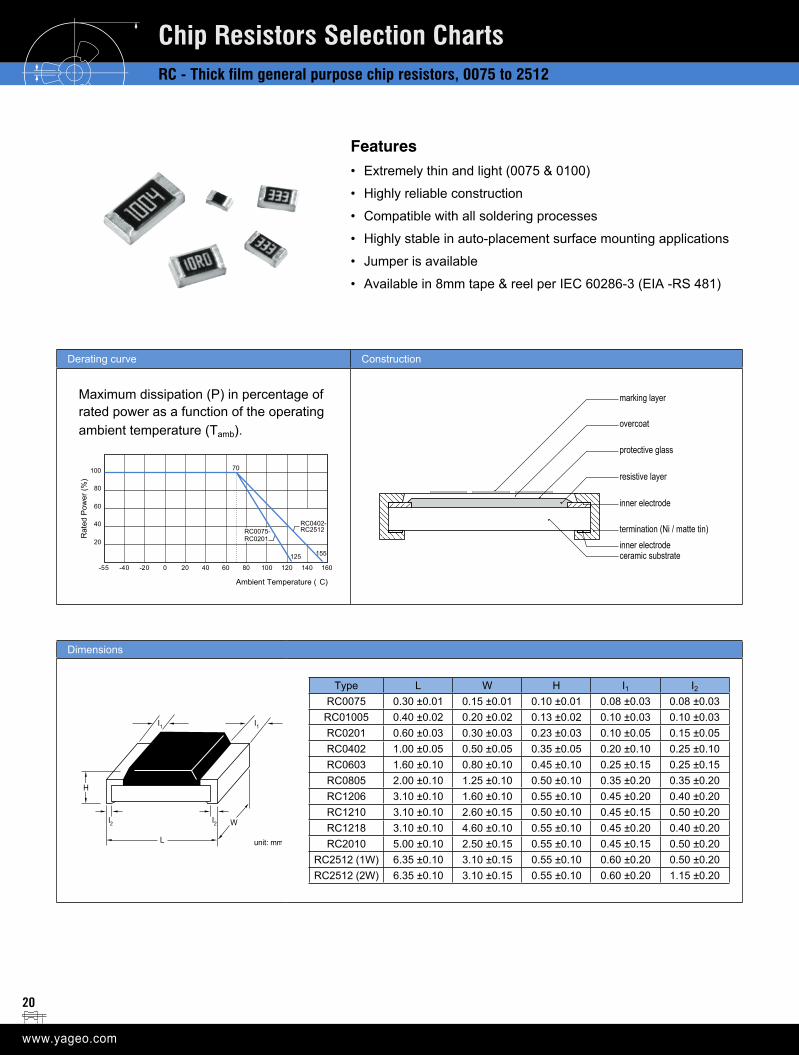
Features• Extremely thin and light (0075 & 0100)
• Highly reliable construction
• Compatible with all soldering processes
• Highly stable in auto-placement surface mounting applications
• Jumper is available
• Available in 8mm tape & reel per IEC 60286-3 (EIA -RS 481)
Derating curve Construction
Maximum dissipation (P) in percentage of rated power as a function of the operating ambient temperature (Tamb).
100
80
60
40
20
-55 -40 -20 0 20 40 60 80
70
100 120 140 160
Ambient Temperature ( C)
Rat
ed P
ower
(%)
155
RC0402-RC2512
125
RC0075-RC0201
overcoat
protective glass
resistive layer
inner electrode
termination (Ni / matte tin)
ceramic substrateinner electrode
marking layer
Dimensions
W
unit: mm
I2
I2
I1
I1
L
H
Type L W H I1 I2RC0075 0.30 ±0.01 0.15 ±0.01 0.10 ±0.01 0.08 ±0.03 0.08 ±0.03RC01005 0.40 ±0.02 0.20 ±0.02 0.13 ±0.02 0.10 ±0.03 0.10 ±0.03RC0201 0.60 ±0.03 0.30 ±0.03 0.23 ±0.03 0.10 ±0.05 0.15 ±0.05RC0402 1.00 ±0.05 0.50 ±0.05 0.35 ±0.05 0.20 ±0.10 0.25 ±0.10RC0603 1.60 ±0.10 0.80 ±0.10 0.45 ±0.10 0.25 ±0.15 0.25 ±0.15RC0805 2.00 ±0.10 1.25 ±0.10 0.50 ±0.10 0.35 ±0.20 0.35 ±0.20RC1206 3.10 ±0.10 1.60 ±0.10 0.55 ±0.10 0.45 ±0.20 0.40 ±0.20RC1210 3.10 ±0.10 2.60 ±0.15 0.50 ±0.10 0.45 ±0.15 0.50 ±0.20RC1218 3.10 ±0.10 4.60 ±0.10 0.55 ±0.10 0.45 ±0.20 0.40 ±0.20RC2010 5.00 ±0.10 2.50 ±0.15 0.55 ±0.10 0.45 ±0.15 0.50 ±0.20
RC2512 (1W) 6.35 ±0.10 3.10 ±0.15 0.55 ±0.10 0.60 ±0.20 0.50 ±0.20RC2512 (2W) 6.35 ±0.10 3.10 ±0.15 0.55 ±0.10 0.60 ±0.20 1.15 ±0.20
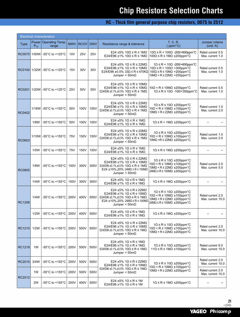
Chip Resistors Selection ChartsRC - Thick film general purpose chip resistors, 0075 to 2512
21
Chip Resistors Selection ChartsRC - Thick film general purpose chip resistors, 0075 to 2512
Electrical characteristics
Type Power P70
Operating Temp. range MWV RCOV DWV Resistance range & tolerance T. C. R.
( ppm/°C) Jumper criteria
(unit: A)
RC0075 1/50W -55°C to +125°C 10V 25V 25V E24 ±5%E24/E96 ±1%
10Ω ≤ R ≤ 1MΩ10Ω ≤ R ≤ 1MΩ
10Ω ≤ R < 100Ω100Ω ≤ R ≤ 1MΩ
-200/+600ppm°C±200ppm°C
Rated current Max. current
0.5 1.0
RC0100 1/32W -55°C to +125°C 15V 30V 30V
E24 ±5%E24/E96 ±1%
E24/E96 ±0.5%Jumper
1Ω ≤ R ≤ 22MΩ1Ω ≤ R ≤ 10MΩ33Ω ≤ R ≤ 470KΩ< 50mΩ
1Ω ≤ R < 10Ω10Ω ≤ R < 100Ω 100Ω ≤ R ≤ 10MΩ10MΩ < R ≤ 22MΩ
-200/+600ppm°C+300ppm°C+200ppm°C+250ppm°C
Rated current Max. current
0.5 1.0
RC0201 1/20W -55°C to +125°C 25V 50V 50V
E24 ±5%E24/E96 ±1%
E24/E96 ±0.1%,±0.5%Jumper
1Ω ≤ R ≤ 10MΩ1Ω ≤ R ≤ 10MΩ10Ω ≤ R ≤ 1MΩ< 50mΩ
10Ω < R ≤ 10MΩ1Ω ≤ R ≤ 10Ω
±200ppm°C-100/+350ppm°C
Rated currentMax. current
0.51.0
RC0402 1/16W -55°C to +155°C 50V 100V 100V
E24 ±5%E24/E96 ±1%
E24/E96 ±0.1%,±0.5%Jumper
1Ω ≤ R ≤ 22MΩ1Ω ≤ R ≤ 10MΩ10Ω ≤ R ≤ 1MΩ< 50mΩ
1Ω ≤ R ≤ 10Ω10Ω < R ≤ 10MΩ 10MΩ < R ≤ 22MΩ
±200ppm°C±100ppm°C±200ppm°C
Rated currentMax. current
1.02.0
1/8W -55°C to +155°C 50V 100V 100V E24 ±5%E24/E96 ±1%
1Ω ≤ R ≤ 1MΩ1Ω ≤ R ≤ 1MΩ 1Ω ≤ R < 1MΩ ±200ppm°C -- --
RC0603 1/10W -55°C to +155°C 75V 150V 150V
E24 ±5%E24/E96 ±1%
E24/E96 ±0.1%,±0.5%Jumper
1Ω ≤ R ≤ 22MΩ1Ω ≤ R ≤ 10MΩ10Ω ≤ R ≤ 1MΩ< 50mΩ
1Ω ≤ R ≤ 10Ω10Ω < R ≤ 10MΩ 10MΩ <R ≤ 22MΩ
±200ppm°C±100ppm°C±200ppm°C
Rated currentMax. current
1.02.0
1/5W -55°C to +155°C 75V 150V 150V E24 ±5%E24/E96 ±1%
1Ω ≤ R ≤ 1MΩ1Ω ≤ R ≤ 1MΩ 1Ω ≤ R ≤ 1MΩ ±200ppm°C -- --
RC0805 1/8W -55°C to +155°C 150V 300V 300V
E24 ±5%E24/E96 ±1%
E24/E96 ±0.1%,±0.5%E24 ±10%,20%
Jumper
1Ω ≤ R ≤ 22MΩ1Ω ≤ R ≤ 10MΩ10Ω ≤ R ≤ 1MΩ24MΩ ≤ R ≤ 100MΩ < 50mΩ
1Ω ≤ R ≤ 10Ω10Ω < R ≤ 10MΩ 10MΩ < R ≤ 22MΩ 24MΩ ≤ R ≤ 100MΩ
±200ppm°C±100ppm°C±200ppm°C±300ppm°C
Rated currentMax. current
2.0 5.0
1/4W -55°C to +155°C 150V 300V 300V E24 ±5%E24/E96 ±1%
1Ω ≤ R ≤ 1MΩ1Ω ≤ R ≤ 1MΩ 1Ω ≤ R ≤ 1MΩ ±200ppm°C -- --
RC1206 1/4W -55°C to +155°C 200V 400V 500V
E24 ±5% E24/E96 ±1%
E24/E96 ±0.1%,±0.5% E24 ±10%,20%
Jumper
1Ω ≤ R ≤ 22MΩ 1Ω ≤ R ≤ 10MΩ 10Ω ≤ R ≤ 1MΩ 24MΩ ≤ R ≤ 100MΩ < 50mΩ
1Ω ≤ R ≤ 10Ω10Ω < R ≤ 10MΩ 10MΩ < R ≤ 22MΩ 24MΩ ≤ R ≤ 100MΩ
±200ppm°C±100ppm°C±200ppm°C±300ppm°C
Rated current Max. current
2.0 10.0
1/2W -55°C to +155°C 200V 400V 500V E24 ±5%E24/E96 ±1%
1Ω ≤ R ≤ 1MΩ1Ω ≤ R ≤ 1MΩ 1Ω ≤ R ≤ 1MΩ ±200ppm°C -- --
RC1210 1/2W -55°C to +155°C 200V 500V 500V
E24 ±5%E24/E96 ±1%
E24/E96 ±0.1%,±0.5%Jumper
1Ω ≤ R ≤ 22MΩ 1Ω ≤ R ≤ 10MΩ 10Ω ≤ R ≤ 1MΩ< 50mΩ
1Ω ≤ R ≤ 10Ω10Ω < R ≤ 10MΩ10MΩ < R ≤ 22MΩ
±200ppm°C±100ppm°C ±200ppm°C
Rated current Max. current
2.0 10.0
RC1218 1W -55°C to +155°C 200V 500V 500V
E24 ±5%E24/E96 ±1%
E24/E96 ±0.1%,±0.5%Jumper
1Ω ≤ R ≤ 1MΩ1Ω ≤ R ≤ 1MΩ10Ω ≤ R ≤ 1MΩ< 50mΩ
1Ω ≤ R ≤ 10Ω11Ω ≤ R ≤ 1MΩ
±200ppm°C±100ppm°C
Rated current Max. current
6.0 10.0
RC2010 3/4W -55°C to +155°C 200V 500V 500V E24 ±5% E24/E96 ±1%
E24/E96 ±0.1%,±0.5% Jumper
1Ω ≤ R ≤ 22MΩ 1Ω ≤ R ≤ 10MΩ 10Ω ≤ R ≤ 1MΩ < 50mΩ
1Ω ≤ R ≤ 10Ω10Ω < R ≤ 10MΩ10MΩ < R ≤ 22MΩ
±200ppm°C±100ppm°C ±200ppm°C
Rated current Max. current
2.0 10.0
RC2512
1W -55°C to +155°C 200V 500V 500V Rated current Max. current
2.0 10.0
2W -55°C to +155°C 200V 400V 500V E24 ±5% E24/E96 ±1%
1Ω ≤ R ≤ 1M 1Ω ≤ R ≤ 1M 1Ω ≤ R ≤ 1MΩ ±200ppm°C -- --
22
Chip Resistors Selection ChartsRC - Thick film general purpose chip resistors, 0075 to 2512
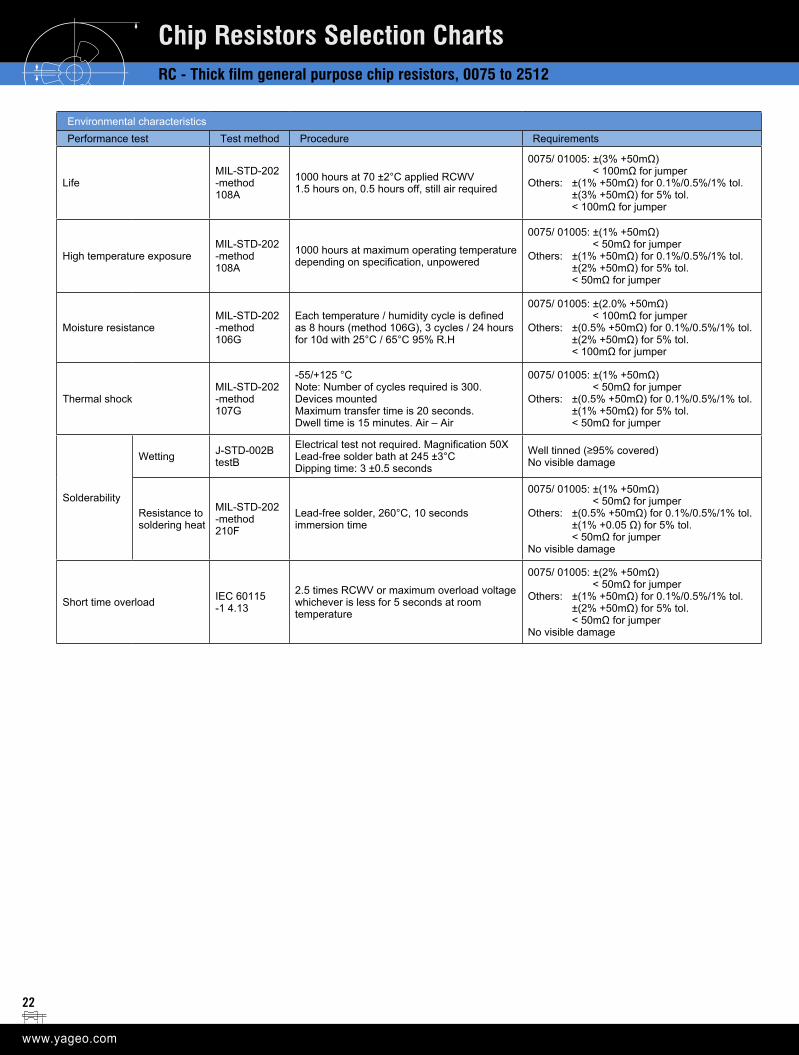
Environmental characteristicsPerformance test Test method Procedure Requirements
LifeMIL-STD-202 -method 108A
1000 hours at 70 ±2°C applied RCWV 1.5 hours on, 0.5 hours off, still air required
0075/ 01005: ±(3% +50mΩ) < 100mΩ for jumperOthers: ±(1% +50mΩ) for 0.1%/0.5%/1% tol. ±(3% +50mΩ) for 5% tol. < 100mΩ for jumper
High temperature exposureMIL-STD-202 -method 108A
1000 hours at maximum operating temperature depending on specification, unpowered
0075/ 01005: ±(1% +50mΩ) < 50mΩ for jumperOthers: ±(1% +50mΩ) for 0.1%/0.5%/1% tol. ±(2% +50mΩ) for 5% tol. < 50mΩ for jumper
Moisture resistanceMIL-STD-202 -method 106G
Each temperature / humidity cycle is defined as 8 hours (method 106G), 3 cycles / 24 hours for 10d with 25°C / 65°C 95% R.H
0075/ 01005: ±(2.0% +50mΩ) < 100mΩ for jumperOthers: ±(0.5% +50mΩ) for 0.1%/0.5%/1% tol. ±(2% +50mΩ) for 5% tol. < 100mΩ for jumper
Thermal shockMIL-STD-202 -method 107G
-55/+125 °CNote: Number of cycles required is 300. Devices mounted Maximum transfer time is 20 seconds. Dwell time is 15 minutes. Air – Air
0075/ 01005: ±(1% +50mΩ) < 50mΩ for jumperOthers: ±(0.5% +50mΩ) for 0.1%/0.5%/1% tol. ±(1% +50mΩ) for 5% tol. < 50mΩ for jumper
Solderability
Wetting J-STD-002B testB
Electrical test not required. Magnification 50X Lead-free solder bath at 245 ±3°C Dipping time: 3 ±0.5 seconds
Well tinned (≥95% covered)No visible damage
Resistance to soldering heat
MIL-STD-202 -method 210F
Lead-free solder, 260°C, 10 secondsimmersion time
0075/ 01005: ±(1% +50mΩ) < 50mΩ for jumperOthers: ±(0.5% +50mΩ) for 0.1%/0.5%/1% tol. ±(1% +0.05 Ω) for 5% tol. < 50mΩ for jumperNo visible damage
Short time overload IEC 60115-1 4.13
2.5 times RCWV or maximum overload voltage whichever is less for 5 seconds at room temperature
0075/ 01005: ±(2% +50mΩ) < 50mΩ for jumperOthers: ±(1% +50mΩ) for 0.1%/0.5%/1% tol. ±(2% +50mΩ) for 5% tol. < 50mΩ for jumperNo visible damage
23
Chip Resistors Selection ChartsRC - Thick film general purpose chip resistors, 0075 to 2512
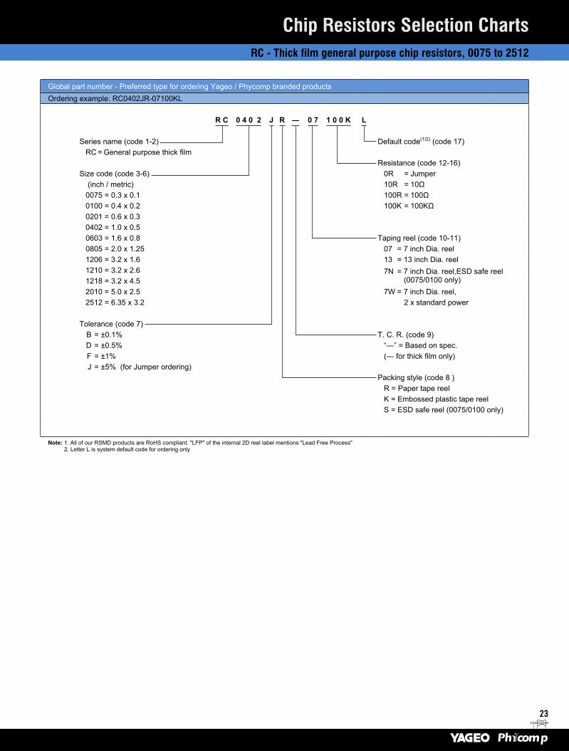
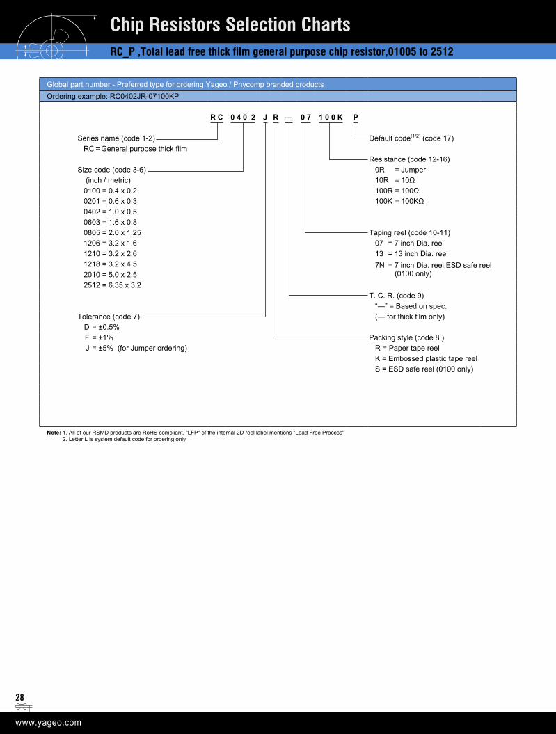
Global part number - Preferred type for ordering Yageo / Phycomp branded productsOrdering example: RC0402JR-07100KL
R C 0 4 0 2 J R ― 0 7 1 0 0 K L
Series name (code 1-2) Default code(1/2) (code 17) RC = General purpose thick film
Resistance (code 12-16)Size code (code 3-6) 0R = Jumper
(inch / metric) 10R = 10Ω0075 = 0.3 x 0.1 100R = 100Ω0100 = 0.4 x 0.2 100K = 100KΩ0201 = 0.6 x 0.30402 = 1.0 x 0.50603 = 1.6 x 0.8 Taping reel (code 10-11)0805 = 2.0 x 1.25 07 = 7 inch Dia. reel1206 = 3.2 x 1.6 13 = 13 inch Dia. reel1210 = 3.2 x 2.6 7N = 7 inch Dia. reel,ESD safe reel
(0075/0100 only) 1218 = 3.2 x 4.52010 = 5.0 x 2.5 7W = 7 inch Dia. reel,2512 = 6.35 x 3.2 2 x standard power
Tolerance (code 7)
B = ±0.1% T. C. R. (code 9) D = ±0.5% “―” = Based on spec. F = ±1% (― for thick film only) J = ±5% (for Jumper ordering)
Packing style (code 8 )R = Paper tape reelK = Embossed plastic tape reelS = ESD safe reel (0075/0100 only)
Note: 1. All of our RSMD products are RoHS compliant. "LFP" of the internal 2D reel label mentions "Lead Free Process" 2. Letter L is system default code for ordering only
24
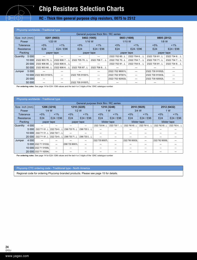
Chip Resistors Selection ChartsRC - Thick film general purpose chip resistors, 0075 to 2512
Phycomp worldwide - Traditional typeGeneral purpose thick film / RC series
Size: inch (mm) 0201 (0603) 0402 (1005) 0603 (1608) 0805 (2012)Power 1/20 W 1/16 W 1/10 W 1/8 W
Tolerance +5% +1% +5% +1% +5% +1% +5% +1%Resistance E24 E24 / E96 E24 E24 / E96 E24 E24 / E96 E24 E24 / E96
Packing paper tape paper tape paper tape paper tapeQuantity 5 000 --- --- --- --- 2322 702 60...L 2322 704 6.…L 2322 730 61...L 2322 734 6.…L
10 000 2322 803 70...L 2322 806 7.…L 2322 705 70...L 2322 706 7.…L 2322 702 70...L 2322 704 7.…L 2322 730 71...L 2322 734 7.…L
20 000 2322 806 80...L 2322 806 8.…L --- --- 2322 702 81...L 2322 704 8.…L 2322 730 81...L 2322 734 8.…L
50 000 2322 803 60...L 2322 806 6.…L 2322 705 87...L 2322 706 8.…L --- --- --- ---Jumper 5 000 --- --- --- --- 2322 702 96001L --- 2322 730 91002L ---
10 000 2322 803 91001L --- 2322 705 91001L --- 2322 702 97001L --- 2322 730 91003L ---
20 000 --- --- --- --- 2322 702 92002L --- 2322 730 92002L ---
50 000 --- --- 2322 705 91007L --- --- --- --- ---
For ordering rules: See page 14 for E24 / E96 values and the last 4 or 3 digits of the 12NC catalogue number
Phycomp worldwide - Traditional typeGeneral purpose thick film / RC series
Size: inch (mm) 1206 (3216) 1210 (3225) 1218 (3248) 2010 (5025) 2512 (6432)Power 1/4 W 1/2 W 1 W 3/4 W 1 W
Tolerance +5% +1% +5% +1% +5% +1% +5% +1% +5% +1%Resistance E24 E24 / E96 E24 E24 / E96 E24 E24 / E96 E24 E24 / E96 E24 E24 / E96
Packing paper tape paper tape blister tape blister tape blister tapeQuantity 4 000 --- --- --- --- 2322 735 64...L 2322 735 7.…L 2322 760 60...L 2322 761 6.…L 2322 762 60...L 2322 763 6.…L
5 000 2322 711 61...L 2322 724 6.…L 2390 735 70...L 2390 735 3.…L --- --- --- --- --- ---
10 000 2322 711 51...L 2322 724 7.…L --- --- --- --- --- --- --- ---
20 000 2322 711 81...L 2322 724 8.…L 2390 735 71...L 2390 735 5.…L --- --- --- --- --- ---Jumper 4 000 --- --- --- --- 2322 735 90007L --- 2322 760 90003L --- 2322 762 90000L ---
5 000 2322 711 91032L --- 2390 735 90001L --- --- --- --- --- --- ---
10 000 2322 711 91005L --- --- --- --- --- --- --- --- ---
20 000 2322 711 92004L --- --- --- --- --- --- --- --- ---
For ordering rules: See page 14 for E24 / E96 values and the last 4 or 3 digits of the 12NC catalogue number
Phycomp CTC ordering code - Traditional type - North America
Regional code for ordering Phycomp branded products. Please see page 15 for details.
25
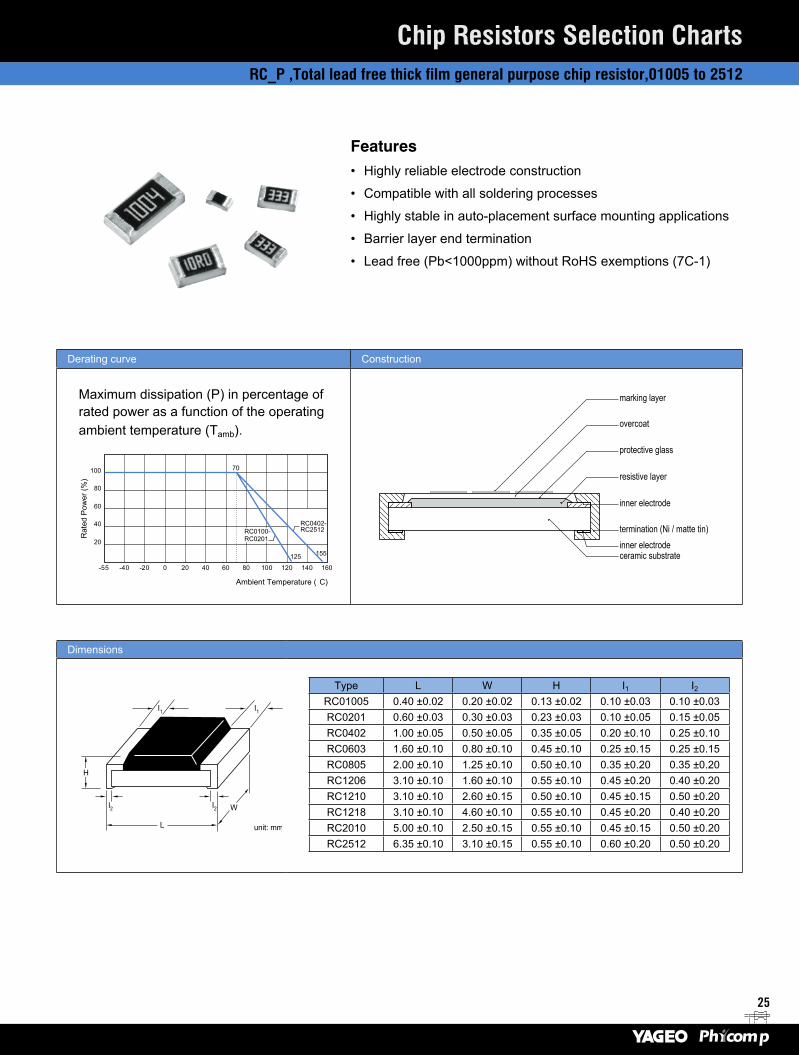
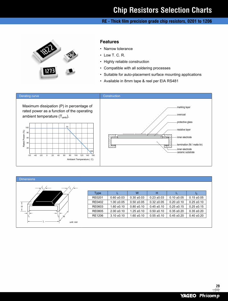
Features• Highly reliable electrode construction
• Compatible with all soldering processes
• Highly stable in auto-placement surface mounting applications
• Barrier layer end termination
• Lead free (Pb<1000ppm) without RoHS exemptions (7C-1)
Derating curve Construction
Maximum dissipation (P) in percentage of rated power as a function of the operating ambient temperature (Tamb).
100
80
60
40
20
-55 -40 -20 0 20 40 60 80
70
100 120 140 160
Ambient Temperature ( C)
Rat
ed P
ower
(%)
155
RC0402-RC2512
125
RC0100-RC0201
overcoat
protective glass
resistive layer
inner electrode
termination (Ni / matte tin)
ceramic substrateinner electrode
marking layer
Dimensions
W
unit: mm
I2
I2
I1
I1
L
H
Type L W H I1 I2RC01005 0.40 ±0.02 0.20 ±0.02 0.13 ±0.02 0.10 ±0.03 0.10 ±0.03RC0201 0.60 ±0.03 0.30 ±0.03 0.23 ±0.03 0.10 ±0.05 0.15 ±0.05RC0402 1.00 ±0.05 0.50 ±0.05 0.35 ±0.05 0.20 ±0.10 0.25 ±0.10RC0603 1.60 ±0.10 0.80 ±0.10 0.45 ±0.10 0.25 ±0.15 0.25 ±0.15RC0805 2.00 ±0.10 1.25 ±0.10 0.50 ±0.10 0.35 ±0.20 0.35 ±0.20RC1206 3.10 ±0.10 1.60 ±0.10 0.55 ±0.10 0.45 ±0.20 0.40 ±0.20RC1210 3.10 ±0.10 2.60 ±0.15 0.50 ±0.10 0.45 ±0.15 0.50 ±0.20RC1218 3.10 ±0.10 4.60 ±0.10 0.55 ±0.10 0.45 ±0.20 0.40 ±0.20RC2010 5.00 ±0.10 2.50 ±0.15 0.55 ±0.10 0.45 ±0.15 0.50 ±0.20RC2512 6.35 ±0.10 3.10 ±0.15 0.55 ±0.10 0.60 ±0.20 0.50 ±0.20
Chip Resistors Selection ChartsRC_P ,Total lead free thick film general purpose chip resistor,01005 to 2512
26
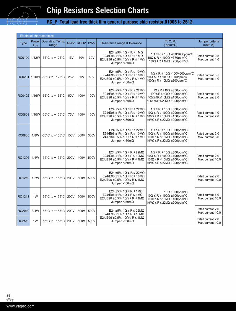
Chip Resistors Selection ChartsRC_P ,Total lead free thick film general purpose chip resistor,01005 to 2512
Electrical characteristics
Type Power P70
Operating Temp. range MWV RCOV DWV Resistance range & tolerance T. C. R.
( ppm/°C) Jumper criteria
(unit: A)
RC0100 1/32W -55°C to +125°C 15V 30V 30V
E24 ±5%E24/E96 ±1%
E24/E96 ±0.5%Jumper
1Ω ≤ R ≤ 1MΩ1Ω ≤ R ≤ 1MΩ10Ω ≤ R ≤ 1MΩ< 50mΩ
1Ω ≤ R < 10Ω10Ω ≤ R < 100Ω 100Ω ≤ R ≤ 1MΩ
-200/+600ppm°C+370ppm°C+250ppm°C
Rated current Max. current
0.5 1.0
RC0201 1/20W -55°C to +125°C 25V 50V 50V
E24 ±5%E24/E96 ±1%
E24/E96 ±0.5%Jumper
1Ω ≤ R ≤ 10MΩ1Ω ≤ R ≤ 10MΩ10Ω ≤ R ≤ 1MΩ< 50mΩ
1Ω ≤ R ≤ 10Ω10Ω ≤ R ≤ 100Ω100Ω ≤ R ≤ 10MΩ
-100/+500ppm°C±300ppm°C±200ppm°C
Rated currentMax. current
0.51.0
RC0402 1/16W -55°C to +155°C 50V 100V 100V
E24 ±5%E24/E96 ±1%
E24/E96 ±0.5%Jumper
1Ω ≤ R ≤ 22MΩ1Ω ≤ R ≤ 10MΩ10Ω ≤ R ≤ 1MΩ< 50mΩ
1Ω ≤ R ≤ 10Ω10Ω ≤ R ≤ 100Ω
100Ω ≤ R ≤ 10MΩ10MΩ ≤ R ≤ 22MΩ
±350ppm°C±200ppm°C±150ppm°C±200ppm°C
Rated currentMax. current
1.02.0
RC0603 1/10W -55°C to +155°C 75V 150V 150V
E24 ±5%E24/E96 ±1%
E24/E96 ±0.5%Jumper
1Ω ≤ R ≤ 22MΩ1Ω ≤ R ≤ 10MΩ10Ω ≤ R ≤ 1MΩ< 50mΩ
1Ω ≤ R ≤ 10Ω10Ω ≤ R ≤ 100Ω100Ω ≤ R ≤ 10MΩ10MΩ ≤ R ≤ 22MΩ
±300ppm°C±200ppm°C±150ppm°C±200ppm°C
Rated currentMax. current
1.02.0
RC0805 1/8W -55°C to +155°C 150V 300V 300V
E24 ±5%E24/E96 ±1%
E24/E96±0.5%Jumper
1Ω ≤ R ≤ 22MΩ1Ω ≤ R ≤ 10MΩ10Ω ≤ R ≤ 1MΩ< 50mΩ
1Ω ≤ R ≤ 10Ω10Ω ≤ R ≤ 100Ω100Ω ≤ R ≤ 10MΩ10MΩ ≤ R ≤ 22MΩ
±300ppm°C±150ppm°C±100ppm°C±200ppm°C
Rated currentMax. current
2.0 5.0
RC1206 1/4W -55°C to +155°C 200V 400V 500V
E24 ±5% E24/E96 ±1%
E24/E96 ±0.5% Jumper
1Ω ≤ R ≤ 22MΩ 1Ω ≤ R ≤ 10MΩ 10Ω ≤ R ≤ 1MΩ < 50mΩ
1Ω ≤ R ≤ 10Ω10Ω ≤ R ≤ 100Ω100Ω ≤ R ≤ 10MΩ10MΩ ≤ R ≤ 22MΩ
±300ppm°C±100ppm°C±100ppm°C±200ppm°C
Rated current Max. current
2.0 10.0
RC1210 1/2W -55°C to +155°C 200V 500V 500V
E24 ±5%E24/E96 ±1%
E24/E96 ±0.5%Jumper
1Ω ≤ R ≤ 22MΩ 1Ω ≤ R ≤ 10MΩ 10Ω ≤ R ≤ 1MΩ< 50mΩ
10Ω10Ω ≤ R ≤ 100Ω100Ω ≤ R ≤ 10MΩ10MΩ ≤ R ≤ 22MΩ
±300ppm°C±100ppm°C±100ppm°C±200ppm°C
Rated current Max. current
2.0 10.0
RC1218 1W -55°C to +155°C 200V 500V 500V
E24 ±5%E24/E96 ±1%
E24/E96 ±0.5%Jumper
1Ω ≤ R ≤ 1MΩ1Ω ≤ R ≤ 1MΩ10Ω ≤ R ≤ 1MΩ< 50mΩ
Rated current Max. current
6.0 10.0
RC2010 3/4W -55°C to +155°C 200V 500V 500V E24 ±5% E24/E96 ±1%
E24/E96 ±0.5% Jumper
1Ω ≤ R ≤ 22MΩ 1Ω ≤ R ≤ 10MΩ 10Ω ≤ R ≤ 1MΩ < 50mΩ
Rated current Max. current
2.0 10.0
RC2512 1W -55°C to +155°C 200V 500V 500V Rated current Max. current
2.0 10.0
27
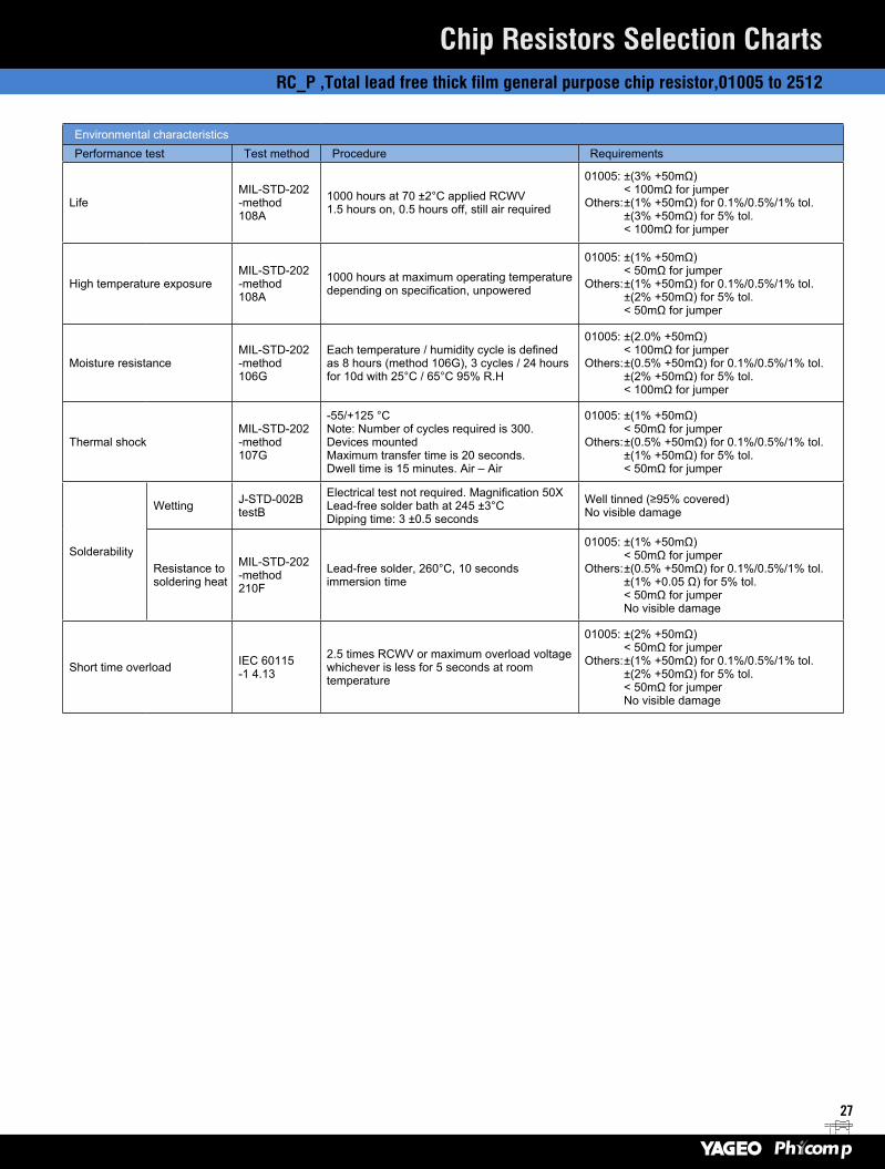
Chip Resistors Selection ChartsRC_P ,Total lead free thick film general purpose chip resistor,01005 to 2512
Environmental characteristicsPerformance test Test method Procedure Requirements
LifeMIL-STD-202 -method 108A
1000 hours at 70 ±2°C applied RCWV 1.5 hours on, 0.5 hours off, still air required
01005: ±(3% +50mΩ) < 100mΩ for jumperOthers:±(1% +50mΩ) for 0.1%/0.5%/1% tol. ±(3% +50mΩ) for 5% tol. < 100mΩ for jumper
High temperature exposureMIL-STD-202 -method 108A
1000 hours at maximum operating temperature depending on specification, unpowered
01005: ±(1% +50mΩ) < 50mΩ for jumperOthers:±(1% +50mΩ) for 0.1%/0.5%/1% tol. ±(2% +50mΩ) for 5% tol. < 50mΩ for jumper
Moisture resistanceMIL-STD-202 -method 106G
Each temperature / humidity cycle is defined as 8 hours (method 106G), 3 cycles / 24 hours for 10d with 25°C / 65°C 95% R.H
01005: ±(2.0% +50mΩ) < 100mΩ for jumperOthers:±(0.5% +50mΩ) for 0.1%/0.5%/1% tol. ±(2% +50mΩ) for 5% tol. < 100mΩ for jumper
Thermal shockMIL-STD-202 -method 107G
-55/+125 °CNote: Number of cycles required is 300. Devices mounted Maximum transfer time is 20 seconds. Dwell time is 15 minutes. Air – Air
01005: ±(1% +50mΩ) < 50mΩ for jumperOthers:±(0.5% +50mΩ) for 0.1%/0.5%/1% tol. ±(1% +50mΩ) for 5% tol. < 50mΩ for jumper
Solderability
Wetting J-STD-002B testB
Electrical test not required. Magnification 50X Lead-free solder bath at 245 ±3°C Dipping time: 3 ±0.5 seconds
Well tinned (≥95% covered)No visible damage
Resistance to soldering heat
MIL-STD-202 -method 210F
Lead-free solder, 260°C, 10 secondsimmersion time
01005: ±(1% +50mΩ) < 50mΩ for jumperOthers:±(0.5% +50mΩ) for 0.1%/0.5%/1% tol. ±(1% +0.05 Ω) for 5% tol. < 50mΩ for jumper No visible damage
Short time overload IEC 60115-1 4.13
2.5 times RCWV or maximum overload voltage whichever is less for 5 seconds at room temperature
01005: ±(2% +50mΩ) < 50mΩ for jumperOthers:±(1% +50mΩ) for 0.1%/0.5%/1% tol. ±(2% +50mΩ) for 5% tol. < 50mΩ for jumper No visible damage
28
Chip Resistors Selection ChartsRC_P ,Total lead free thick film general purpose chip resistor,01005 to 2512
Global part number - Preferred type for ordering Yageo / Phycomp branded productsOrdering example: RC0402JR-07100KP
R C 0 4 0 2 J R ― 0 7 1 0 0 K P
Series name (code 1-2) Default code(1/2) (code 17) RC = General purpose thick film
Resistance (code 12-16)Size code (code 3-6) 0R = Jumper
(inch / metric) 10R = 10Ω0100 = 0.4 x 0.2 100R = 100Ω0201 = 0.6 x 0.3 100K = 100KΩ0402 = 1.0 x 0.50603 = 1.6 x 0.80805 = 2.0 x 1.25 Taping reel (code 10-11)1206 = 3.2 x 1.6 07 = 7 inch Dia. reel1210 = 3.2 x 2.6 13 = 13 inch Dia. reel1218 = 3.2 x 4.5 7N = 7 inch Dia. reel,ESD safe reel
(0100 only) 2010 = 5.0 x 2.52512 = 6.35 x 3.2
T. C. R. (code 9)“―” = Based on spec.
Tolerance (code 7) (― for thick film only) D = ±0.5% F = ±1% Packing style (code 8 ) J = ±5% (for Jumper ordering) R = Paper tape reel
K = Embossed plastic tape reelS = ESD safe reel (0100 only)
Note: 1. All of our RSMD products are RoHS compliant. "LFP" of the internal 2D reel label mentions "Lead Free Process" 2. Letter L is system default code for ordering only
29
Features• Narrow tolerance
• Low T. C. R.
• Highly reliable construction
• Compatible with all soldering processes
• Suitable for auto-placement surface mounting applications
• Available in 8mm tape & reel per EIA RS481
Derating curve Construction
Maximum dissipation (P) in percentage of rated power as a function of the operating ambient temperature (Tamb).
overcoat
protective glass
resistive layer
inner electrode
termination (Ni / matte tin)
ceramic substrateinner electrode
marking layer
Dimensions
Type L W H I1 I2RE0201 0.60 ±0.03 0.30 ±0.03 0.23 ±0.03 0.10 ±0.05 0.15 ±0.05RE0402 1.00 ±0.05 0.50 ±0.05 0.32 ±0.05 0.20 ±0.10 0.25 ±0.10RE0603 1.60 ±0.10 0.80 ±0.10 0.45 ±0.10 0.25 ±0.15 0.25 ±0.15RE0805 2.00 ±0.10 1.25 ±0.10 0.50 ±0.10 0.35 ±0.20 0.35 ±0.20RE1206 3.10 ±0.10 1.60 ±0.10 0.55 ±0.10 0.45 ±0.20 0.40 ±0.20
Chip Resistors Selection ChartsRE - Thick film precision grade chip resistors, 0201 to 1206
100
80
60
40
20
-55 -40 -20 0 20 40 60 80
70
100 120 140 160
Ambient Temperature ( C)
Rat
ed P
ower
(%)
155
W
unit: mm
I2
I2
I1
I1
L
H
30
Chip Resistors Selection ChartsRE - Thick film precision grade chip resistors, 0201 to 1206
Electrical characteristics
Type Power P70
Operating Temp. range MWV RCOV DWV Resistance range & tolerance T. C. R.
RE0201 1/20W -55°C to +155°C 25V 50V 50V
E24/E96 ±0.1%,±0.5%, ±1% 10Ω ≤ R ≤ 1MΩ ±50 ppm/°C
RE0402 1/16W -55°C to +155°C 50V 100V 100V
RE0603 1/10W -55°C to +155°C 75V 150V 150V
RE0805 1/8W -55°C to +155°C 150V 300V 300V
RE1206 1/4W -55°C to +155°C 200V 400V 500V
Environmental characteristicsPerformance test Test method Procedure Requirements
Life MIL-STD-202 -method 108A
1000 hours at 70 ±2°C applied RCWV 1.5 hours on, 0.5 hours off, still air required ±(3% +50mΩ)
High temperature exposure MIL-STD-202 -method 108A
1000 hours at maximum operating temperature depending on specification, unpowered ±(3% +50mΩ)
Moisture resistance MIL-STD-202 -method 106G
Each temperature / humidity cycle is defined as 8 hours (method 106G), 3 cycles / 24 hours for 10d with 25°C / 65°C 95% R.H
±(3% +50mΩ)
Thermal shock MIL-STD-202 -method 107G
-55/+125 °CNote: Number of cycles required is 300. Devices mounted Maximum transfer time is 20 seconds. Dwell time is 15 minutes. Air – Air
±(1% +50mΩ)
Solderability Wetting
IPC/JEDECJ-STD-002B testB
Electrical test not required. Magnification 50X Lead-free solder bath at 245 ±3°C Dipping time: 3 ±0.5 seconds
Well tinned (≥95% covered)No visible damage
Resistance to soldering heat
MIL-STD-202 -method 210F Lead-free solder, 260°C, 10 seconds immersion time ±(0.5%+ 50mΩ)
No visible damage
Short time overload IEC 60115-1 4.13
2.5 times RCWV or maximum overload voltage whichever is less for 5 seconds at room temperature
±(1%+ 50mΩ) No visible damage
31
Chip Resistors Selection ChartsRE - Thick film precision grade chip resistors, 0201 to 1206
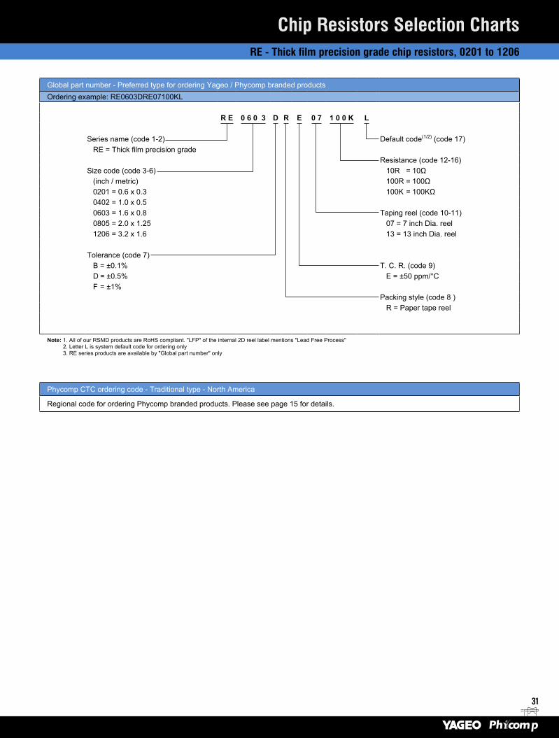
Global part number - Preferred type for ordering Yageo / Phycomp branded productsOrdering example: RE0603DRE07100KL
R E 0 6 0 3 D R E 0 7 1 0 0 K L
Series name (code 1-2) Default code(1/2) (code 17) RE = Thick film precision grade
Resistance (code 12-16)Size code (code 3-6) 10R = 10Ω
(inch / metric) 100R = 100Ω0201 = 0.6 x 0.3 100K = 100KΩ0402 = 1.0 x 0.50603 = 1.6 x 0.8 Taping reel (code 10-11)0805 = 2.0 x 1.25 07 = 7 inch Dia. reel1206 = 3.2 x 1.6 13 = 13 inch Dia. reel
Tolerance (code 7)B = ±0.1% T. C. R. (code 9)D = ±0.5% E = ±50 ppm/°CF = ±1%
Packing style (code 8 )R = Paper tape reel
Note: 1. All of our RSMD products are RoHS compliant. "LFP" of the internal 2D reel label mentions "Lead Free Process" 2. Letter L is system default code for ordering only 3. RE series products are available by "Global part number" only
Phycomp CTC ordering code - Traditional type - North America
Regional code for ordering Phycomp branded products. Please see page 15 for details.
32
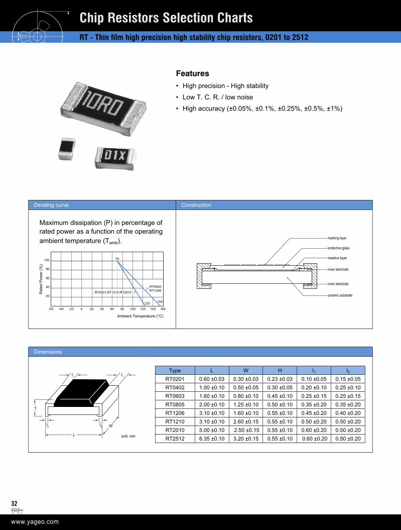
Derating curve Construction
Maximum dissipation (P) in percentage of rated power as a function of the operating ambient temperature (Tamb).
100
80
60
40
20
-55 -40 -20 0 20 40 60 80
70
100 120 140 160
Ambient Temperature (°C)
Rat
ed P
ower
(%)
155
RT0402-RT1206
125
RT0201,RT1210-RT2512
protective glass
marking layer
resistive layer
inner electrode
ceramic substrate
inner electrode
Dimensions
Type L W H I1 I2
RT0201 0.60 ±0.03 0.30 ±0.03 0.23 ±0.03 0.10 ±0.05 0.15 ±0.05RT0402 1.00 ±0.10 0.50 ±0.05 0.30 ±0.05 0.20 ±0.10 0.25 ±0.10RT0603 1.60 ±0.10 0.80 ±0.10 0.45 ±0.10 0.25 ±0.15 0.25 ±0.15RT0805 2.00 ±0.10 1.25 ±0.10 0.50 ±0.10 0.35 ±0.20 0.35 ±0.20RT1206 3.10 ±0.10 1.60 ±0.10 0.55 ±0.10 0.45 ±0.20 0.40 ±0.20RT1210 3.10 ±0.10 2.60 ±0.15 0.55 ±0.10 0.50 ±0.20 0.50 ±0.20RT2010 5.00 ±0.10 2.50 ±0.15 0.55 ±0.10 0.60 ±0.20 0.50 ±0.20RT2512 6.35 ±0.10 3.20 ±0.15 0.55 ±0.10 0.60 ±0.20 0.50 ±0.20
Features• High precision - High stability
• Low T. C. R. / low noise
• High accuracy (±0.05%, ±0.1%, ±0.25%, ±0.5%, ±1%)
Chip Resistors Selection ChartsRT - Thin film high precision high stability chip resistors, 0201 to 2512
W
unit: mm
I2
I2
I1
I1
L
H
33
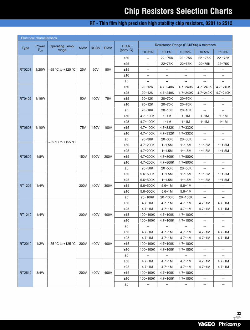
Electrical characteristics
Type Power P70
Operating Temp. range MWV RCOV DWV T.C.R.
(ppm/°C)Resistance Range (E24/E96) & tolerance
±0.05% ±0.1% ±0.25% ±0.5% ±1.0%
RT0201 1/20W –55 °C to +125 °C 25V 50V 50V
±50 -- 22 ~75K 22 ~75K 22 ~75K 22 ~75K
±25 -- 22~75K 22~75K 22~75K 22~75K
±15 -- -- -- -- --
±10 -- -- -- -- --
±5 -- -- -- -- --
RT0402 1/16W
–55 °C to +155 °C
50V 100V 75V
±50 20~12K 4.7~240K 4.7~240K 4.7~240K 4.7~240K
±25 20~12K 4.7~240K 4.7~240K 4.7~240K 4.7~240K
±15 20~12K 20~70K 20~70K -- --
±10 20~12K 20~70K 20~70K -- --
±5 20~10K 20~10K 20~10K -- --
RT0603 1/10W 75V 150V 100V
±50 4.7~100K 1~1M 1~1M 1~1M 1~1M
±25 4.7~100K 1~1M 1~1M 1~1M 1~1M
±15 4.7~100K 4.7~332K 4.7~332K -- --
±10 4.7~100K 4.7~332K 4.7~332K -- --
±5 20~30K 20~30K 20~30K -- --
RT0805 1/8W 150V 300V 200V
±50 4.7~200K 1~1.5M 1~1.5M 1~1.5M 1~1.5M
±25 4.7~200K 1~1.5M 1~1.5M 1~1.5M 1~1.5M
±15 4.7~200K 4.7~800K 4.7~800K -- --
±10 4.7~200K 4.7~800K 4.7~800K -- --
±5 20~50K 20~50K 20~50K -- --
RT1206 1/4W 200V 400V 300V
±50 5.6~500K 1~1.5M 1~1.5M 1~1.5M 1~1.5M
±25 5.6~500K 1~1.5M 1~1.5M 1~1.5M 1~1.5M
±15 5.6~500K 5.6~1M 5.6~1M -- --
±10 5.6~500K 5.6~1M 5.6~1M -- --
±5 20~100K 20~100K 20~100K -- --
RT1210 1/4W
–55 °C to +125 °C
200V 400V 400V
±50 4.7~1M 4.7~1M 4.7~1M 4.7~1M 4.7~1M
±25 4.7~1M 4.7~1M 4.7~1M 4.7~1M 4.7~1M
±15 100~100K 4.7~100K 4.7~100K -- --
±10 100~100K 4.7~100K 4.7~100K -- --
±5 -- -- -- -- --
RT2010 1/2W 200V 400V 400V
±50 4.7~1M 4.7~1M 4.7~1M 4.7~1M 4.7~1M
±25 4.7~1M 4.7~1M 4.7~1M 4.7~1M 4.7~1M
±15 100~100K 4.7~100K 4.7~100K -- --
±10 100~100K 4.7~100K 4.7~100K -- --
±5 -- -- -- -- --
RT2512 3/4W 200V 400V 400V
±50 4.7~1M 4.7~1M 4.7~1M 4.7~1M 4.7~1M
±25 4.7~1M 4.7~1M 4.7~1M 4.7~1M 4.7~1M
±15 100~100K 4.7~100K 4.7~100K -- --
±10 100~100K 4.7~100K 4.7~100K -- --
±5 -- -- -- -- --
Chip Resistors Selection ChartsRT - Thin film high precision high stability chip resistors, 0201 to 2512
34
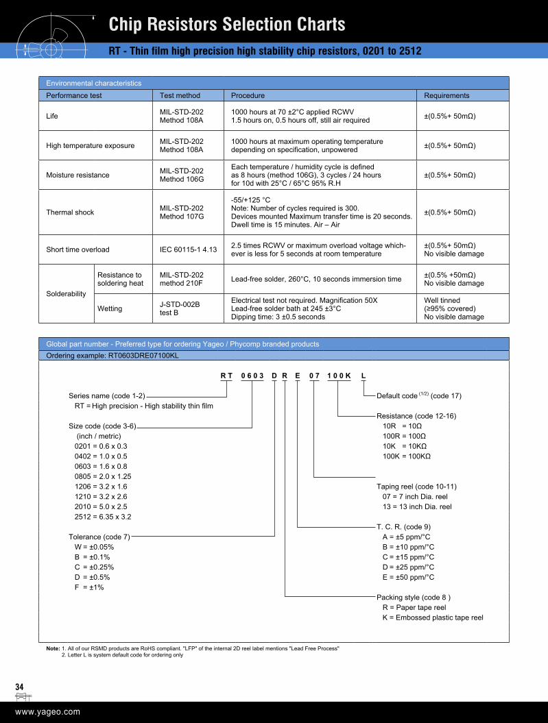
Environmental characteristics
Performance test Test method Procedure Requirements
Life MIL-STD-202 Method 108A
1000 hours at 70 ±2°C applied RCWV 1.5 hours on, 0.5 hours off, still air required ±(0.5%+ 50mΩ)
High temperature exposure MIL-STD-202 Method 108A
1000 hours at maximum operating temperature depending on specification, unpowered ±(0.5%+ 50mΩ)
Moisture resistance MIL-STD-202 Method 106G
Each temperature / humidity cycle is defined as 8 hours (method 106G), 3 cycles / 24 hours for 10d with 25°C / 65°C 95% R.H
±(0.5%+ 50mΩ)
Thermal shock MIL-STD-202 Method 107G
-55/+125 °CNote: Number of cycles required is 300. Devices mounted Maximum transfer time is 20 seconds. Dwell time is 15 minutes. Air – Air
±(0.5%+ 50mΩ)
Short time overload IEC 60115-1 4.13 2.5 times RCWV or maximum overload voltage which-ever is less for 5 seconds at room temperature
±(0.5%+ 50mΩ)No visible damage
Solderability
Resistance to soldering heat
MIL-STD-202 method 210F Lead-free solder, 260°C, 10 seconds immersion time ±(0.5% +50mΩ)
No visible damage
Wetting J-STD-002B test B
Electrical test not required. Magnification 50X Lead-free solder bath at 245 ±3°C Dipping time: 3 ±0.5 seconds
Well tinned (≥95% covered)No visible damage
Global part number - Preferred type for ordering Yageo / Phycomp branded productsOrdering example: RT0603DRE07100KL
R T 0 6 0 3 D R E 0 7 1 0 0 K L
Series name (code 1-2) Default code (1/2) (code 17) RT = High precision - High stability thin film
Resistance (code 12-16)Size code (code 3-6) 10R = 10Ω
(inch / metric) 100R = 100Ω0201 = 0.6 x 0.3 10K = 10KΩ0402 = 1.0 x 0.5 100K = 100KΩ0603 = 1.6 x 0.8 0805 = 2.0 x 1.251206 = 3.2 x 1.6 Taping reel (code 10-11)1210 = 3.2 x 2.6 07 = 7 inch Dia. reel2010 = 5.0 x 2.5 13 = 13 inch Dia. reel2512 = 6.35 x 3.2
T. C. R. (code 9)Tolerance (code 7) A = ±5 ppm/°C
W = ±0.05% B = ±10 ppm/°C B = ±0.1% C = ±15 ppm/°C C = ±0.25% D = ±25 ppm/°CD = ±0.5% E = ±50 ppm/°CF = ±1% Packing style (code 8 )
R = Paper tape reelK = Embossed plastic tape reel
Note: 1. All of our RSMD products are RoHS compliant. "LFP" of the internal 2D reel label mentions "Lead Free Process" 2. Letter L is system default code for ordering only
Chip Resistors Selection ChartsRT - Thin film high precision high stability chip resistors, 0201 to 2512
35
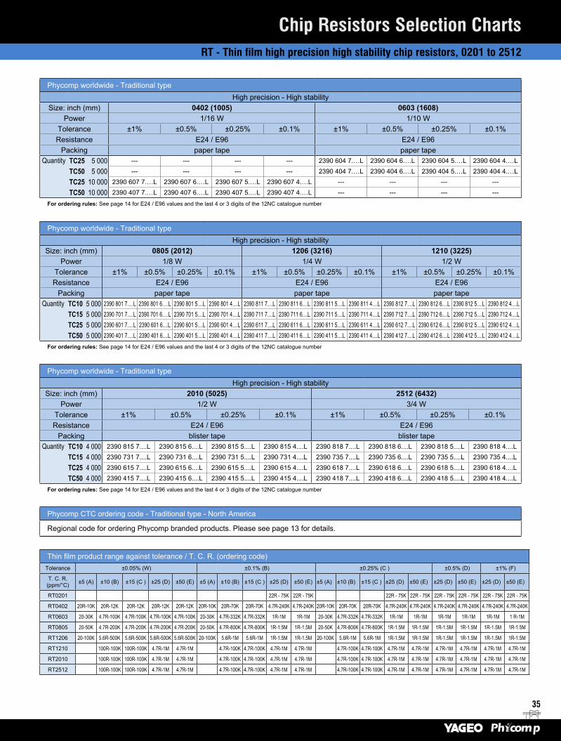
Phycomp worldwide - Traditional typeHigh precision - High stability
Size: inch (mm) 0402 (1005) 0603 (1608)Power 1/16 W 1/10 W
Tolerance ±1% ±0.5% ±0.25% ±0.1% ±1% ±0.5% ±0.25% ±0.1%Resistance E24 / E96 E24 / E96
Packing paper tape paper tapeQuantity TC25 5 000 --- --- --- --- 2390 604 7.…L 2390 604 6.…L 2390 604 5.…L 2390 604 4.…L
TC50 5 000 --- --- --- --- 2390 404 7.…L 2390 404 6.…L 2390 404 5.…L 2390 404 4.…L
TC25 10 000 2390 607 7.…L 2390 607 6.…L 2390 607 5.…L 2390 607 4.…L --- --- --- ---
TC50 10 000 2390 407 7.…L 2390 407 6.…L 2390 407 5.…L 2390 407 4.…L --- --- --- ---
For ordering rules: See page 14 for E24 / E96 values and the last 4 or 3 digits of the 12NC catalogue number
Phycomp worldwide - Traditional typeHigh precision - High stability
Size: inch (mm) 0805 (2012) 1206 (3216) 1210 (3225)Power 1/8 W 1/4 W 1/2 W
Tolerance ±1% ±0.5% ±0.25% ±0.1% ±1% ±0.5% ±0.25% ±0.1% ±1% ±0.5% ±0.25% ±0.1%Resistance E24 / E96 E24 / E96 E24 / E96
Packing paper tape paper tape paper tapeQuantity TC10 5 000 2390 801 7.…L 2390 801 6.…L 2390 801 5....L 2390 801 4....L 2390 811 7....L 2390 811 6....L 2390 811 5....L 2390 811 4....L 2390 812 7....L 2390 812 6....L 2390 812 5....L 2390 812 4....L
TC15 5 000 2390 701 7.…L 2390 701 6.…L 2390 701 5....L 2390 701 4....L 2390 711 7....L 2390 711 6....L 2390 711 5....L 2390 711 4....L 2390 712 7....L 2390 712 6....L 2390 712 5....L 2390 712 4....L
TC25 5 000 2390 601 7.…L 2390 601 6....L 2390 601 5....L 2390 601 4....L 2390 611 7....L 2390 611 6....L 2390 611 5....L 2390 611 4....L 2390 612 7....L 2390 612 6....L 2390 612 5....L 2390 612 4....L
TC50 5 000 2390 401 7.…L 2390 401 6....L 2390 401 5....L 2390 401 4....L 2390 411 7....L 2390 411 6....L 2390 411 5....L 2390 411 4....L 2390 412 7....L 2390 412 6....L 2390 412 5....L 2390 412 4....L
For ordering rules: See page 14 for E24 / E96 values and the last 4 or 3 digits of the 12NC catalogue number
Phycomp worldwide - Traditional typeHigh precision - High stability
Size: inch (mm) 2010 (5025) 2512 (6432)Power 1/2 W 3/4 W
Tolerance ±1% ±0.5% ±0.25% ±0.1% ±1% ±0.5% ±0.25% ±0.1%Resistance E24 / E96 E24 / E96
Packing blister tape blister tapeQuantity TC10 4 000 2390 815 7....L 2390 815 6....L 2390 815 5....L 2390 815 4....L 2390 818 7....L 2390 818 6....L 2390 818 5....L 2390 818 4....L
TC15 4 000 2390 731 7....L 2390 731 6....L 2390 731 5....L 2390 731 4....L 2390 735 7....L 2390 735 6....L 2390 735 5....L 2390 735 4....L
TC25 4 000 2390 615 7....L 2390 615 6....L 2390 615 5....L 2390 615 4....L 2390 618 7....L 2390 618 6....L 2390 618 5....L 2390 618 4....L
TC50 4 000 2390 415 7....L 2390 415 6....L 2390 415 5....L 2390 415 4....L 2390 418 7....L 2390 418 6....L 2390 418 5....L 2390 418 4....L
For ordering rules: See page 14 for E24 / E96 values and the last 4 or 3 digits of the 12NC catalogue number
Phycomp CTC ordering code - Traditional type - North America
Regional code for ordering Phycomp branded products. Please see page 13 for details.
Thin film product range against tolerance / T. C. R. (ordering code)Tolerance ±0.05% (W) ±0.1% (B) ±0.25% (C ) ±0.5% (D) ±1% (F)
T. C. R. (ppm/°C) ±5 (A) ±10 (B) ±15 (C ) ±25 (D) ±50 (E) ±5 (A) ±10 (B) ±15 (C ) ±25 (D) ±50 (E) ±5 (A) ±10 (B) ±15 (C ) ±25 (D) ±50 (E) ±25 (D) ±50 (E) ±25 (D) ±50 (E)
RT0201 22R - 75K 22R - 75K 22R - 75K 22R - 75K 22R - 75K 22R - 75K 22R - 75K 22R - 75K
RT0402 20R-10K 20R-12K 20R-12K 20R-12K 20R-12K 20R-10K 20R-70K 20R-70K 4.7R-240K 4.7R-240K 20R-10K 20R-70K 20R-70K 4.7R-240K 4.7R-240K 4.7R-240K 4.7R-240K 4.7R-240K 4.7R-240K
RT0603 20-30K 4.7R-100K 4.7R-100K 4.7R-100K 4.7R-100K 20-30K 4.7R-332K 4.7R-332K 1R-1M 1R-1M 20-30K 4.7R-332K 4.7R-332K 1R-1M 1R-1M 1R-1M 1R-1M 1R-1M 1 R-1M
RT0805 20-50K 4.7R-200K 4.7R-200K 4.7R-200K 4.7R-200K 20-50K 4.7R-800K 4.7R-800K 1R-1.5M 1R-1.5M 20-50K 4.7R-800K 4.7R-800K 1R-1.5M 1R-1.5M 1R-1.5M 1R-1.5M 1R-1.5M 1R-1.5M
RT1206 20-100K 5.6R-500K 5.6R-500K 5.6R-500K 5.6R-500K 20-100K 5.6R-1M 5.6R-1M 1R-1.5M 1R-1.5M 20-100K 5.6R-1M 5.6R-1M 1R-1.5M 1R-1.5M 1R-1.5M 1R-1.5M 1R-1.5M 1R-1.5M
RT1210 100R-100K 100R-100K 4.7R-1M 4.7R-1M 4.7R-100K 4.7R-100K 4.7R-1M 4.7R-1M 4.7R-100K 4.7R-100K 4.7R-1M 4.7R-1M 4.7R-1M 4.7R-1M 4.7R-1M 4.7R-1M
RT2010 100R-100K 100R-100K 4.7R-1M 4.7R-1M 4.7R-100K 4.7R-100K 4.7R-1M 4.7R-1M 4.7R-100K 4.7R-100K 4.7R-1M 4.7R-1M 4.7R-1M 4.7R-1M 4.7R-1M 4.7R-1M
RT2512 100R-100K 100R-100K 4.7R-1M 4.7R-1M 4.7R-100K 4.7R-100K 4.7R-1M 4.7R-1M 4.7R-100K 4.7R-100K 4.7R-1M 4.7R-1M 4.7R-1M 4.7R-1M 4.7R-1M 4.7R-1M
Chip Resistors Selection ChartsRT - Thin film high precision high stability chip resistors, 0201 to 2512
36
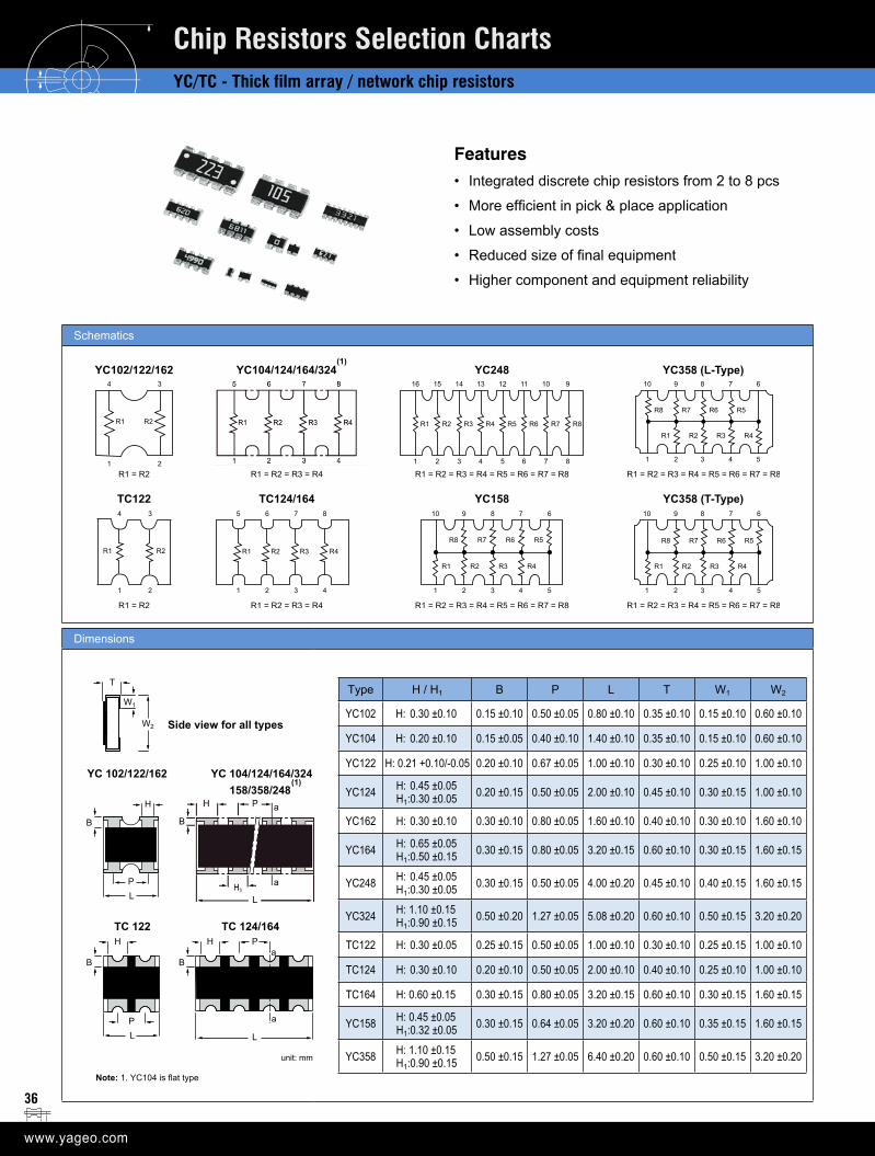
Schematics
Dimensions
Side view for all types
T
W1
W2
YC 102/122/162
H
B
PL
YC 104/124/164/324 158/358/248
H
L
B
H1
a
a
P
L
TC 122
PL
B
HTC 124/164
B
Ha
a
P
unit: mm
Type H / H1 B P L T W1 W2
YC102 H: 0.30 ±0.10 0.15 ±0.10 0.50 ±0.05 0.80 ±0.10 0.35 ±0.10 0.15 ±0.10 0.60 ±0.10
YC104 H: 0.20 ±0.10 0.15 ±0.05 0.40 ±0.10 1.40 ±0.10 0.35 ±0.10 0.15 ±0.10 0.60 ±0.10
YC122 H: 0.21 +0.10/-0.05 0.20 ±0.10 0.67 ±0.05 1.00 ±0.10 0.30 ±0.10 0.25 ±0.10 1.00 ±0.10
YC124 H: 0.45 ±0.05H1:0.30 ±0.05 0.20 ±0.15 0.50 ±0.05 2.00 ±0.10 0.45 ±0.10 0.30 ±0.15 1.00 ±0.10
YC162 H: 0.30 ±0.10 0.30 ±0.10 0.80 ±0.05 1.60 ±0.10 0.40 ±0.10 0.30 ±0.10 1.60 ±0.10
YC164 H: 0.65 ±0.05H1:0.50 ±0.15 0.30 ±0.15 0.80 ±0.05 3.20 ±0.15 0.60 ±0.10 0.30 ±0.15 1.60 ±0.15
YC248 H: 0.45 ±0.05 H1:0.30 ±0.05 0.30 ±0.15 0.50 ±0.05 4.00 ±0.20 0.45 ±0.10 0.40 ±0.15 1.60 ±0.15
YC324 H: 1.10 ±0.15 H1:0.90 ±0.15 0.50 ±0.20 1.27 ±0.05 5.08 ±0.20 0.60 ±0.10 0.50 ±0.15 3.20 ±0.20
TC122 H: 0.30 ±0.05 0.25 ±0.15 0.50 ±0.05 1.00 ±0.10 0.30 ±0.10 0.25 ±0.15 1.00 ±0.10
TC124 H: 0.30 ±0.10 0.20 ±0.10 0.50 ±0.05 2.00 ±0.10 0.40 ±0.10 0.25 ±0.10 1.00 ±0.10
TC164 H: 0.60 ±0.15 0.30 ±0.15 0.80 ±0.05 3.20 ±0.15 0.60 ±0.10 0.30 ±0.15 1.60 ±0.15
YC158 H: 0.45 ±0.05H1:0.32 ±0.05 0.30 ±0.15 0.64 ±0.05 3.20 ±0.20 0.60 ±0.10 0.35 ±0.15 1.60 ±0.15
YC358 H: 1.10 ±0.15 H1:0.90 ±0.15 0.50 ±0.15 1.27 ±0.05 6.40 ±0.20 0.60 ±0.10 0.50 ±0.15 3.20 ±0.20
Features• Integrated discrete chip resistors from 2 to 8 pcs
• More efficient in pick & place application
• Low assembly costs
• Reduced size of final equipment
• Higher component and equipment reliability
Chip Resistors Selection ChartsYC/TC - Thick film array / network chip resistors
Note: 1. YC104 is flat type
37
Electrical characteristics
Type Power P70
Operating Temp. range MWV RCOV DWV Resistance range & tolerance T. C. R. Jumper criteria
(unit: A)
YC102 1/32W -55°C to +125°C 15V 30V 30VE24 ±5%
E24/E96 ±1% Jumper
10Ω ≤ R ≤ 1MΩ10Ω ≤ R ≤ 1MΩ < 50mΩ
±200 ppm/°C
Rated current Max. current
0.5 1.0
YC104 1/32W -55°C to +125°C 12.5V 25V 25VE24 ±5%
E24/E96 ±1%Jumper
10Ω ≤ R ≤ 1MΩ10Ω ≤ R ≤ 1MΩ< 50mΩ
Rated current Max. current
0.5 1.0
YC122 1/16W -55°C to +155°C 50V 100V 100VE24 ±5%
E24/E96 ±1% Jumper
1Ω ≤ R ≤ 1MΩ1Ω ≤ R ≤ 1MΩ < 50mΩ
1Ω ≤ R ≤ 10Ω ±250 ppm/°C10Ω ≤ R ≤ 1MΩ ±200 ppm/°C
Rated current Max. current
0.5 1.0
YC124 1/16W -55°C to +155°C 25V 50V 100VE24 ±5%
E24/E96 ±1% Jumper
1Ω ≤ R ≤ 1MΩ1Ω ≤ R ≤ 1MΩ < 50mΩ
Rated current Max. current
1.0 2.0
YC162 1/16W -55°C to +155°C 50V 100V 100VE24/E96 ±1%
E24 ±5% Jumper
1Ω ≤ R ≤ 1MΩ1Ω ≤ R ≤ 1MΩ < 50mΩ
Rated current Max. current
1.0 2.0
YC164 1/16W -55°C to +155°C 50V 100V 100VE24 ±5%
E24/E96 ±1% Jumper
1Ω ≤ R ≤ 1MΩ1Ω ≤ R ≤ 1MΩ< 50mΩ
±200 ppm/°C
Rated current Max. current
1.0 2.0
YC248 1/16W -55°C to +155°C 50V 100V 100VE24 ±5%
E24/E96 ±1% Jumper
10Ω ≤ R ≤ 1MΩ10Ω ≤ R ≤ 1MΩ< 50mΩ
Rated current Max. current
2.0 10.0
YC324 1/8W -55°C to +155°C 200V 500V 500V E24 ±5% E24/E96 ±1%
10Ω ≤ R ≤ 1MΩ10Ω ≤ R ≤ 1MΩ -- --
TC122 1/16W -55°C to +125°C 50V 100V 100VE24 ±5%
E24/E96 ±1% Jumper
10Ω ≤ R ≤ 1MΩ10Ω ≤ R ≤ 1MΩ < 50mΩ
Rated current Max. current
1.0 1.5
TC124 1/16W -55°C to +125°C 50V 100V 100VE24 ±5%
E24/E96 ±1% Jumper
10Ω ≤ R ≤ 1MΩ10Ω ≤ R ≤ 1MΩ < 50mΩ
Rated current Max. current
1.0 1.5
TC164 1/16W -55°C to +155°C 50V 100V 100VE24 ±5%
E24/E96 ±1% Jumper
10Ω ≤ R ≤ 1MΩ10Ω ≤ R ≤ 1MΩ < 50mΩ
Rated current Max. current
1.0 2.0
YC158 1/16W -55°C to +155°C 25V 50V 50V E24 ±5% 10Ω ≤ R ≤ 100KΩ -- --
YC358 1/16W -55°C to +155°C 50V 100V 100V E24 ±5% 10Ω ≤ R ≤ 330KΩ -- --
Environmental characteristicsPerformance test Test method Procedure Requirements
Life MIL-STD-202 Method 108A
1000 hours at 70 ±2°C applied RCWV 1.5 hours on, 0.5 hours off, still air required
±(2% +50mΩ) < 100mΩ for jumper
High temperature exposure MIL-STD-202 Method 108A
1000 hours at maximum operating temperature depending on specification, unpowered
±(1% +50mΩ) < 50mΩ for jumper
Moisture resistance MIL-STD-202 Method 106G
Each temperature / humidity cycle is defined as 8 hours(method 106G), 3 cycles / 24 hours for 10d with25°C / 65°C 95% R.H
±(2% +50mΩ) < 100mΩ for jumper
Thermal shock MIL-STD-202 Method 107G
-55/+125 °CNote: Number of cycles required is 300. Devices mounted Maximum transfer time is 20 seconds. Dwell time is 15 minutes. Air – Air
±(1% +50mΩ) for others< 50mΩ for jumper
Solderability
Wetting J-STD-002B test B
Electrical test not required. Magnification 50X Lead-free solder bath at 245 ±3°C Dipping time: 3 ±0.5 seconds
Well tinned (≥95% covered)
Resistance to soldering heat
MIL-STD-202 method 210F Lead-free solder, 260°C, 10 seconds immersion time
±(1% +50mΩ) < 50mΩ for jumperNo visible damage
Short time overload IEC 60115-1 4.13
2.5 times RCWV or maximum overload voltage whichever is less for 5 seconds at room temperature
±(2% +50mΩ) < 50mΩ for jumperNo visible damage
Chip Resistors Selection ChartsYC/TC - Thick film array / network chip resistors
38
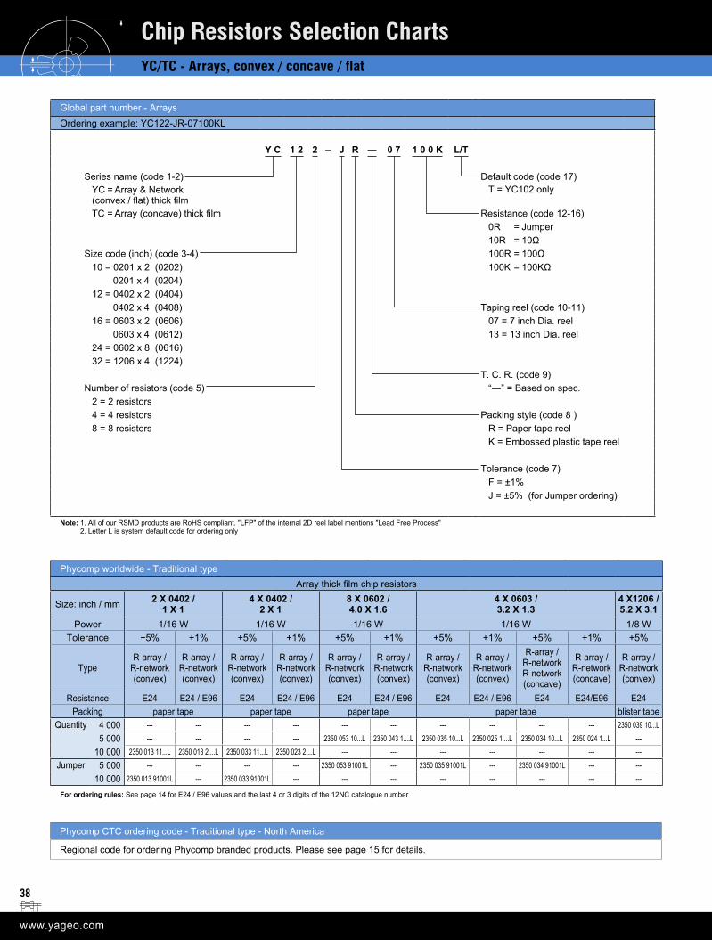
Global part number - ArraysOrdering example: YC122-JR-07100KL
Y C 1 2 2 ― J R ― 0 7 1 0 0 K L/T
Series name (code 1-2) Default code (code 17) YC = Array & Network (convex / flat) thick film
T = YC102 only
TC = Array (concave) thick film Resistance (code 12-16)0R = Jumper 10R = 10Ω
Size code (inch) (code 3-4) 100R = 100Ω10 = 0201 x 2 (0202) 100K = 100KΩ 0201 x 4 (0204) 12 = 0402 x 2 (0404) 0402 x 4 (0408) Taping reel (code 10-11)16 = 0603 x 2 (0606) 07 = 7 inch Dia. reel 0603 x 4 (0612) 13 = 13 inch Dia. reel 24 = 0602 x 8 (0616)32 = 1206 x 4 (1224)
T. C. R. (code 9)Number of resistors (code 5) “―” = Based on spec.
2 = 2 resistors4 = 4 resistors Packing style (code 8 )8 = 8 resistors R = Paper tape reel
K = Embossed plastic tape reel
Tolerance (code 7)F = ±1%J = ±5% (for Jumper ordering)
Note: 1. All of our RSMD products are RoHS compliant. "LFP" of the internal 2D reel label mentions "Lead Free Process" 2. Letter L is system default code for ordering only
Phycomp worldwide - Traditional typeArray thick film chip resistors
Size: inch / mm 2 X 0402 / 1 X 1
4 X 0402 / 2 X 1
8 X 0602 / 4.0 X 1.6
4 X 0603 / 3.2 X 1.3
4 X1206 / 5.2 X 3.1
Power 1/16 W 1/16 W 1/16 W 1/16 W 1/8 WTolerance +5% +1% +5% +1% +5% +1% +5% +1% +5% +1% +5%
TypeR-array /
R-network (convex)
R-array / R-network (convex)
R-array / R-network (convex)
R-array / R-network (convex)
R-array / R-network (convex)
R-array / R-network (convex)
R-array / R-network (convex)
R-array / R-network (convex)
R-array / R-network R-network(concave)
R-array /R-network(concave)
R-array / R-network (convex)
Resistance E24 E24 / E96 E24 E24 / E96 E24 E24 / E96 E24 E24 / E96 E24 E24/E96 E24Packing paper tape paper tape paper tape paper tape blister tape
Quantity 4 000 --- --- --- --- --- --- --- --- --- --- 2350 039 10...L
5 000 --- --- --- --- 2350 053 10...L 2350 043 1....L 2350 035 10...L 2350 025 1....L 2350 034 10...L 2350 024 1...L ---
10 000 2350 013 11...L 2350 013 2....L 2350 033 11...L 2350 023 2....L --- --- --- --- --- --- ---Jumper 5 000 --- --- --- --- 2350 053 91001L --- 2350 035 91001L --- 2350 034 91001L --- ---
10 000 2350 013 91001L --- 2350 033 91001L --- --- --- --- --- --- --- ---
For ordering rules: See page 14 for E24 / E96 values and the last 4 or 3 digits of the 12NC catalogue number
Phycomp CTC ordering code - Traditional type - North America
Regional code for ordering Phycomp branded products. Please see page 15 for details.
Chip Resistors Selection ChartsYC/TC - Arrays, convex / concave / flat
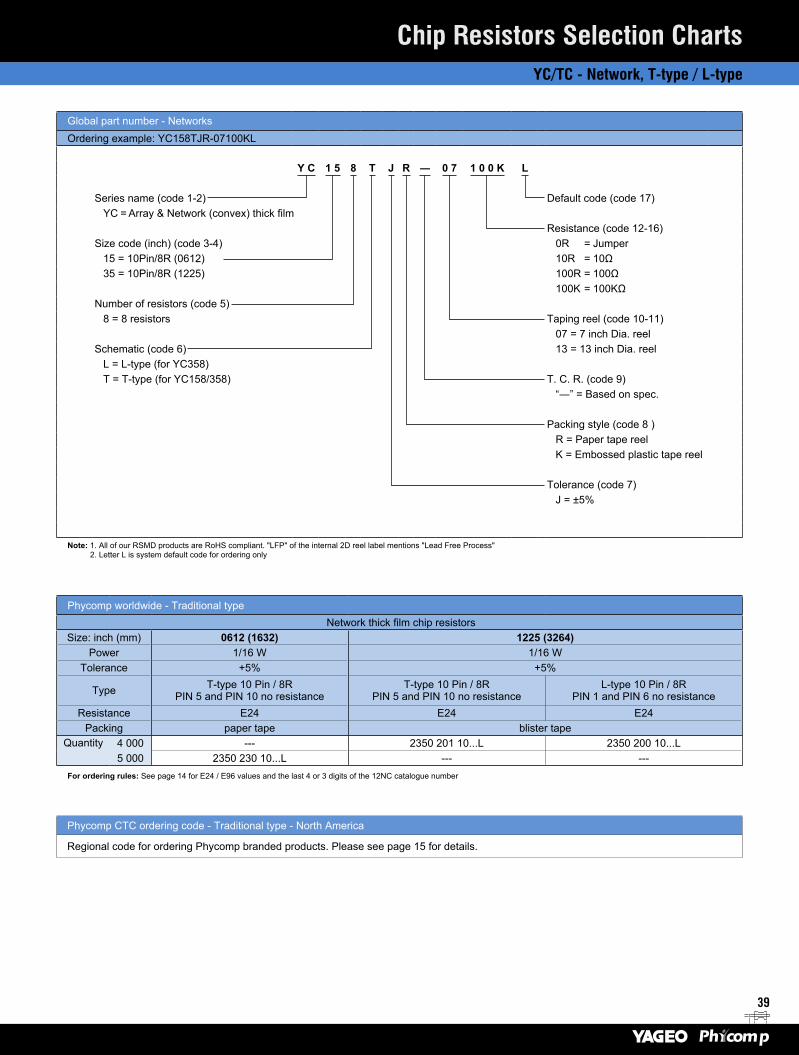
39
Global part number - NetworksOrdering example: YC158TJR-07100KL
Y C 1 5 8 T J R ― 0 7 1 0 0 K L
Series name (code 1-2) Default code (code 17) YC = Array & Network (convex) thick film
Resistance (code 12-16)Size code (inch) (code 3-4) 0R = Jumper
15 = 10Pin/8R (0612) 10R = 10Ω35 = 10Pin/8R (1225) 100R = 100Ω
100K = 100KΩNumber of resistors (code 5)
8 = 8 resistors Taping reel (code 10-11)07 = 7 inch Dia. reel
Schematic (code 6) 13 = 13 inch Dia. reelL = L-type (for YC358)T = T-type (for YC158/358) T. C. R. (code 9)
“―” = Based on spec.
Packing style (code 8 )R = Paper tape reelK = Embossed plastic tape reel
Tolerance (code 7)J = ±5%
Note: 1. All of our RSMD products are RoHS compliant. "LFP" of the internal 2D reel label mentions "Lead Free Process" 2. Letter L is system default code for ordering only
Phycomp worldwide - Traditional type Network thick film chip resistors
Size: inch (mm) 0612 (1632) 1225 (3264)Power 1/16 W 1/16 W
Tolerance +5% +5%
Type T-type 10 Pin / 8R PIN 5 and PIN 10 no resistance
T-type 10 Pin / 8R PIN 5 and PIN 10 no resistance
L-type 10 Pin / 8R PIN 1 and PIN 6 no resistance
Resistance E24 E24 E24Packing paper tape blister tape
Quantity 4 000 --- 2350 201 10...L 2350 200 10...L 5 000 2350 230 10...L --- ---
For ordering rules: See page 14 for E24 / E96 values and the last 4 or 3 digits of the 12NC catalogue number
Phycomp CTC ordering code - Traditional type - North America
Regional code for ordering Phycomp branded products. Please see page 15 for details.
Chip Resistors Selection ChartsYC/TC - Network, T-type / L-type
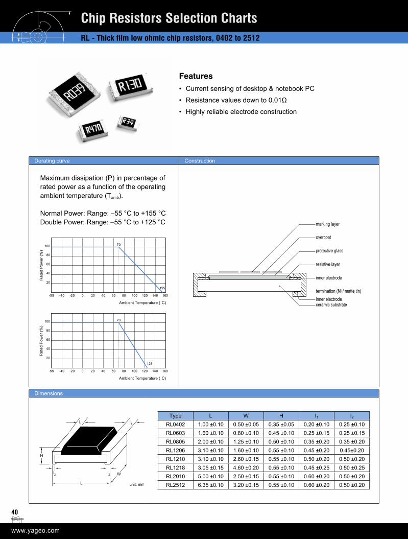
40
Derating curve Construction
Maximum dissipation (P) in percentage of rated power as a function of the operating ambient temperature (Tamb).
Normal Power: Range: –55 °C to +155 °C Double Power: Range: –55 °C to +125 °C
Dimensions
W
unit: mm
I2
I2
I1
I1
L
H
Type L W H I1 I2RL0402 1.00 ±0.10 0.50 ±0.05 0.35 ±0.05 0.20 ±0.10 0.25 ±0.10 RL0603 1.60 ±0.10 0.80 ±0.10 0.45 ±0.10 0.25 ±0.15 0.25 ±0.15 RL0805 2.00 ±0.10 1.25 ±0.10 0.50 ±0.10 0.35 ±0.20 0.35 ±0.20 RL1206 3.10 ±0.10 1.60 ±0.10 0.55 ±0.10 0.45 ±0.20 0.45±0.20 RL1210 3.10 ±0.10 2.60 ±0.15 0.55 ±0.10 0.50 ±0.20 0.50 ±0.20 RL1218 3.05 ±0.15 4.60 ±0.20 0.55 ±0.10 0.45 ±0.25 0.50 ±0.25 RL2010 5.00 ±0.10 2.50 ±0.15 0.55 ±0.10 0.60 ±0.20 0.50 ±0.20 RL2512 6.35 ±0.10 3.20 ±0.15 0.55 ±0.10 0.60 ±0.20 0.50 ±0.20
100
80
60
40
20
-55 -40 -20 0 20 40 60 80
70
100 120 140 160
Ambient Temperature ( C)
Rat
ed P
ower
(%)
155
Chip Resistors Selection ChartsRL - Thick film low ohmic chip resistors, 0402 to 2512
Features• Current sensing of desktop & notebook PC
• Resistance values down to 0.01Ω
• Highly reliable electrode construction
overcoat
protective glass
resistive layer
inner electrode
termination (Ni / matte tin)
ceramic substrateinner electrode
marking layer
100
80
60
40
20
-55 -40 -20 0 20 40 60 80
70
100 120 140 160
Ambient Temperature ( C)
Rat
ed P
ower
(%)
125
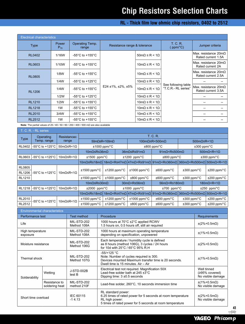
41
Chip Resistors Selection ChartsRL - Thick film low ohmic chip resistors, 0402 to 2512
Electrical characteristics
Type Power P70
Operating Temp. range Resistance range & tolerance T. C. R.
( ppm/°C) Jumper criteria
RL0402 1/16W -55°C to +155°C
E24 ±1%, ±2%, ±5%
50mΩ ≤ R < 1Ω
See following table “T.C.R.- RL series”
Max. resistanceRated current
20mΩ1.5A
RL0603 1/10W -55°C to +155°C 10mΩ ≤ R < 1Ω Max. resistanceRated current
20mΩ2A
RL0805 1/8W -55°C to +155°C 10mΩ ≤ R < 1Ω Max. resistance
Rated current20mΩ2.5A
1/4W -55°C to +125°C 10mΩ ≤ R < 1Ω -- --
RL1206 1/4W -55°C to +155°C 10mΩ ≤ R < 1Ω Max. resistance
Rated current20mΩ3.5A
1/2W -55°C to +125°C 10mΩ ≤ R < 1Ω -- --
RL1210 1/2W -55°C to +155°C 10mΩ ≤ R < 1Ω -- --
RL1218 1W -55°C to +155°C 10mΩ ≤ R < 1Ω -- --
RL2010 3/4W -55°C to +155°C 10mΩ ≤ R < 1Ω -- --
RL2512 1W -55°C to +155°C 10mΩ ≤ R < 1Ω -- --Note: The partial values of 25 / 40 / 50 / 60 / 250 / 400 / 500 mΩ are also available
T. C. R. - RL series
Type Operating Temp. range
Resistancec range
T. C. R.50mΩ≤R<100mΩ 100mΩ≤R<500mΩ 500mΩ≤R<1Ω
RL0402 -55°C to +125°C 50mΩ≤R<1Ω ±1000 ppm/°C ±800 ppm/°C ±300 ppm/°C10mΩ≤R≤36mΩ 36mΩ≤R≤91mΩ 91mΩ<R≤500mΩ 500mΩ<R<1Ω
RL0603 -55°C to +125°C 10mΩ≤R<1Ω ±1500 ppm/°C ±1200 ppm/°C ±800 ppm/°C ±300 ppm/°C10mΩ≤R≤18mΩ 18mΩ<R≤47mΩ 47mΩ<R≤91mΩ 91mΩ<R≤360mΩ 360mΩ<R≤500mΩ 500mΩ<R<1Ω
RL0805 -55°C to +125°C 10mΩ≤R<1Ω
±1500 ppm/°C ±1200 ppm/°C ±1000 ppm/°C ±600 ppm/°C ±300 ppm/°C ±200 ppm/°CRL1206RL1210 ±1500 ppm/°C ±1000 ppm/°C ±800 ppm/°C ±600 ppm/°C ±300 ppm/°C ±200 ppm/°C
10mΩ≤R≤30mΩ 30mΩ<R≤56mΩ 56mΩ<R≤180mΩ 180mΩ<R<1ΩRL1218 -55°C to +125°C 10mΩ≤R<1Ω ±2000 ppm/°C ±1000 ppm/°C ±700 ppm/°C ±250 ppm/°C
10mΩ≤R≤18mΩ 18mΩ<R≤47mΩ 47mΩ<R≤91mΩ 91mΩ<R≤360mΩ 360mΩ<R≤500mΩ 500mΩ<R<1ΩRL2010
-55°C to +125°C 10mΩ≤R<1Ω±1500 ppm/°C ±1200 ppm/°C ±1000 ppm/°C ±600 ppm/°C ±300 ppm/°C ±200 ppm/°C
RL2512 ±1500 ppm/°C ±1200 ppm/°C ±800 ppm/°C ±600 ppm/°C ±300 ppm/°C ±200 ppm/°C
Environmental characteristics
Performance test Test method Procedure Requirements
Life MIL-STD-202 Method 108A
1000 hours at 70°C ±2°C applied RCWV 1.5 hours on, 0.5 hours off, still air required ±(2%+0.5mΩ)
High temperature exposure
MIL-STD-202 Method 108A
1000 hours at maximum operating temperature depending on specification, unpowered ±(1%+0.5mΩ)
Moisture resistance MIL-STD-202 Method 106G
Each temperature / humidity cycle is defined as 8 hours (method 106G), 3 cycles / 24 hours for 10d with 25°C / 65°C 95% R.H
±(2%+0.5mΩ)
Thermal shock MIL-STD-202 Method 107G
-55/+125 °CNote: Number of cycles required is 300.Devices mounted Maximum transfer time is 20 seconds. Dwell time is 15 minutes. Air – Air
±(1%+0.5mΩ)
Solderability Wetting J-STD-002B
test B
Electrical test not required. Magnification 50X Lead-free solder bath at 245 ±3°C Dipping time: 3 ±0.5 seconds
Well tinned (≥95% covered)No visible damage
Resistance to soldering heat
MIL-STD-202 method 210F Lead-free solder, 260°C, 10 seconds immersion time ±(1%+0.5mΩ)
No visible damage
Short time overload IEC 60115-1 4.13
RL standard power:6.25 times of rated power for 5 seconds at room temperatureRL high power:5 times of rated power for 5 seconds at room temperature
±(2%+0.5mΩ)No visible damage
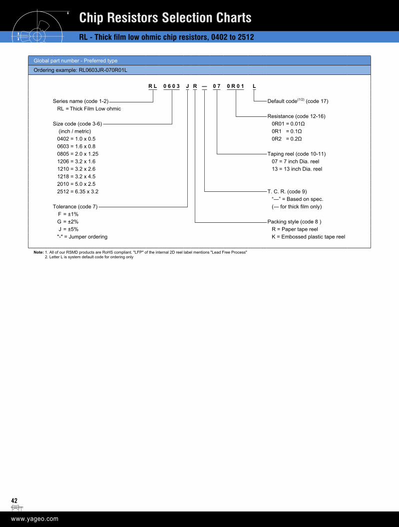
42
Chip Resistors Selection ChartsRL - Thick film low ohmic chip resistors, 0402 to 2512
Global part number - Preferred type
Ordering example: RL0603JR-070R01L
R L 0 6 0 3 J R ― 0 7 0 R 0 1 L
Series name (code 1-2) Default code(1/2) (code 17) RL = Thick Film Low ohmic
Resistance (code 12-16)Size code (code 3-6) 0R01 = 0.01Ω
(inch / metric) 0R1 = 0.1Ω0402 = 1.0 x 0.5 0R2 = 0.2Ω0603 = 1.6 x 0.80805 = 2.0 x 1.25 Taping reel (code 10-11)1206 = 3.2 x 1.6 07 = 7 inch Dia. reel1210 = 3.2 x 2.6 13 = 13 inch Dia. reel1218 = 3.2 x 4.52010 = 5.0 x 2.52512 = 6.35 x 3.2 T. C. R. (code 9)
“―” = Based on spec.Tolerance (code 7) (― for thick film only)
F = ±1% G = ±2% Packing style (code 8 ) J = ±5% R = Paper tape reel"-" = Jumper ordering K = Embossed plastic tape reel
Note: 1. All of our RSMD products are RoHS compliant. "LFP" of the internal 2D reel label mentions "Lead Free Process" 2. Letter L is system default code for ordering only
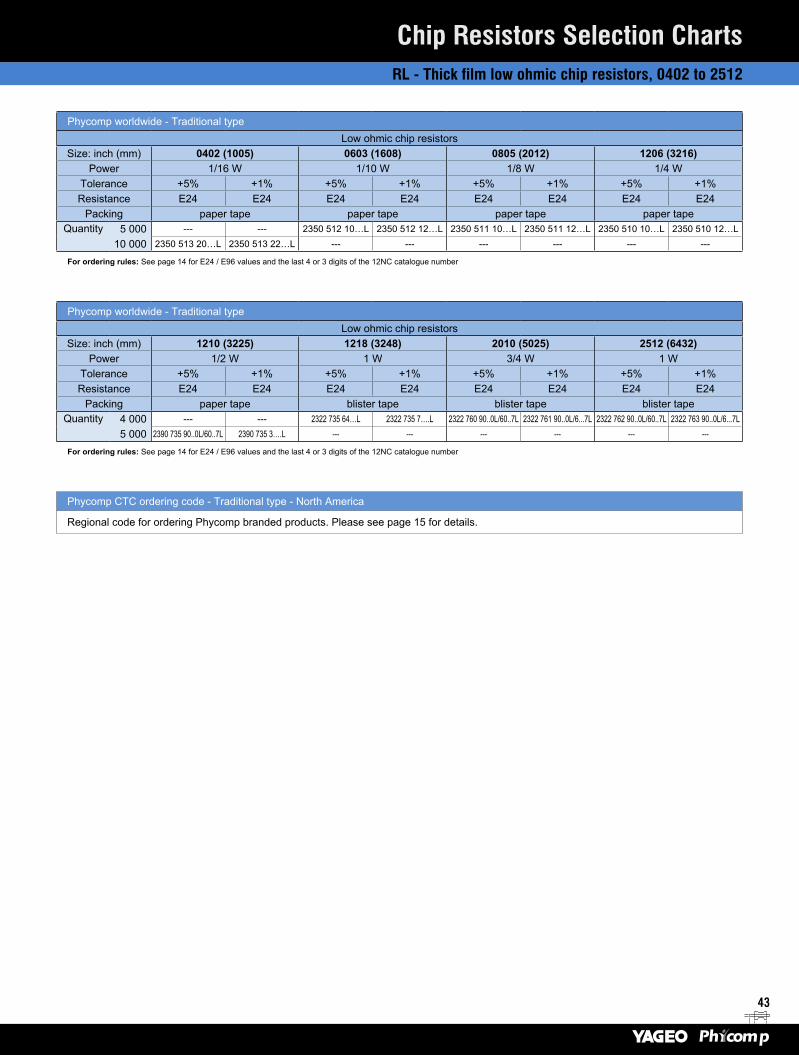
43
Chip Resistors Selection ChartsRL - Thick film low ohmic chip resistors, 0402 to 2512
Phycomp worldwide - Traditional typeLow ohmic chip resistors
Size: inch (mm) 0402 (1005) 0603 (1608) 0805 (2012) 1206 (3216)Power 1/16 W 1/10 W 1/8 W 1/4 W
Tolerance +5% +1% +5% +1% +5% +1% +5% +1%Resistance E24 E24 E24 E24 E24 E24 E24 E24
Packing paper tape paper tape paper tape paper tapeQuantity 5 000 --- --- 2350 512 10…L 2350 512 12…L 2350 511 10…L 2350 511 12…L 2350 510 10…L 2350 510 12…L
10 000 2350 513 20…L 2350 513 22…L --- --- --- --- --- ---
For ordering rules: See page 14 for E24 / E96 values and the last 4 or 3 digits of the 12NC catalogue number
Phycomp worldwide - Traditional typeLow ohmic chip resistors
Size: inch (mm) 1210 (3225) 1218 (3248) 2010 (5025) 2512 (6432)Power 1/2 W 1 W 3/4 W 1 W
Tolerance +5% +1% +5% +1% +5% +1% +5% +1%Resistance E24 E24 E24 E24 E24 E24 E24 E24
Packing paper tape blister tape blister tape blister tapeQuantity 4 000 --- --- 2322 735 64…L 2322 735 7….L 2322 760 90..0L/60..7L 2322 761 90..0L/6...7L 2322 762 90..0L/60..7L 2322 763 90..0L/6...7L
5 000 2390 735 90..0L/60..7L 2390 735 3….L --- --- --- --- --- ---
For ordering rules: See page 14 for E24 / E96 values and the last 4 or 3 digits of the 12NC catalogue number
Phycomp CTC ordering code - Traditional type - North America
Regional code for ordering Phycomp branded products. Please see page 15 for details.
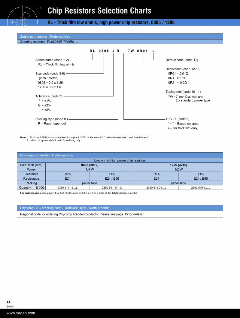
44
Global part number - Preferred typeOrdering example: RL0805JR-7W0R01L
R L 0 8 0 5 J R ― 7 W 0 R 0 1 L
Series name (code 1-2) Default code (code 17) RL = Thick film low ohmic
Resistance (code 12-16)Size code (code 3-6) 0R01 = 0.01Ω
(inch / metric) 0R1 = 0.1Ω0805 = 2.0 x 1.25 0R2 = 0.2Ω1206 = 3.2 x 1.6
Taping reel (code 10-11)Tolerance (code 7) 7W = 7 inch Dia. reel and
2 x standard power type F = ±1% G = ±2% J = ±5%
Packing style (code 8 ) T. C. R. (code 9)R = Paper tape reel “―” = Based on spec.
(― for thick film only)
Note: 1. All of our RSMD products are RoHS compliant. "LFP" of the internal 2D reel label mentions "Lead Free Process" 2. Letter L is system default code for ordering only
Phycomp worldwide - Traditional typeLow ohmic high power chip resistors
Size: inch (mm) 0805 (2012) 1206 (3216)Power 1/4 W 1/2 W
Tolerance +5% +1% +5% +1%Resistance E24 E24 / E96 E24 E24 / E96
Packing paper tape paper tapeQuantity 5 000 2350 511 15…L 2350 511 17…L 2350 519 01…L 2350 519 1.…L
For ordering rules: See page 14 for E24 / E96 values and the last 4 or 3 digits of the 12NC catalogue number
Phycomp CTC ordering code - Traditional type - North America
Regional code for ordering Phycomp branded products. Please see page 15 for details.
Chip Resistors Selection ChartsRL - Thick film low ohmic, high power chip resistors, 0805 / 1206
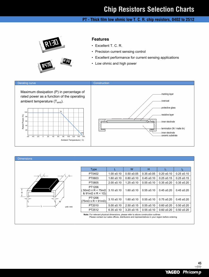
45
Chip Resistors Selection ChartsPT - Thick film low ohmic low T. C. R. chip resistors, 0402 to 2512
Features• Excellent T. C. R.
• Precision current sensing control
• Excellent performance for current sensing applications
• Low ohmic and high power
Derating curve Construction
Maximum dissipation (P) in percentage of rated power as a function of the operating ambient temperature (Tamb).
100
80
60
40
20
-55 -40 -20 0 20 40 60 80
70
100 120 140 160
Ambient Temperature ( C)
Rat
ed P
ower
(%)
155
Dimensions
W
unit: mm
I2
I2
I1
I1
L
H
Type L W H l1 l2PT0402 1.00 ±0.10 0.50 ±0.05 0.35 ±0.05 0.20 ±0.10 0.25 ±0.10PT0603 1.60 ±0.10 0.80 ±0.10 0.45 ±0.10 0.25 ±0.15 0.25 ±0.15PT0805 2.00 ±0.10 1.25 ±0.10 0.55 ±0.10 0.35 ±0.20 0.35 ±0.20PT1206
( 50mΩ ≤ R < 75mΩ & 91mΩ ≤ R < 1Ω)
3.10 ±0.10 1.60 ±0.10 0.55 ±0.10 0.45 ±0.20 0.45 ±0.20
PT1206(75mΩ ≤ R < 91mΩ) 3.10 ±0.10 1.60 ±0.10 0.55 ±0.10 0.75 ±0.20 0.45 ±0.20
PT2010 5.00 ±0.10 2.50 ±0.15 0.55 ±0.10 0.60 ±0.20 0.50 ±0.20PT2512 6.35 ±0.10 3.20 ±0.15 0.55 ±0.10 0.60 ±0.20 0.50 ±0.20
Note: For relevant physical dimensions, please refer to above construction outlines Please contact our sales offices, distributors and representatives in your region before ordering
overcoat
protective glass
resistive layer
inner electrode
termination (Ni / matte tin)
ceramic substrateinner electrode
marking layer
46
Electrical characteristics
Type Power P70
Operating Temp. range
Max. working voltage Tolerance Resistance range & T. C. R. Jumper criteria
PT04021/16W
-55°C to +155°C (PxR)^1/2 E24 ±2%, ±5%E24/E96 ±1%
50mΩ ≤ R < 68mΩ68mΩ ≤ R < 100mΩ
100mΩ ≤ R < 1Ω
±600 ppm/°C±300 ppm/°C±200 ppm/°C
Max. resistanceRated current
10mΩ3A
1/8W
PT0603
1/10W 50mΩ50mΩ < R < 68mΩ
68mΩ ≤ R < 100mΩ100mΩ ≤ R < 1Ω
0/+400 ppm/°C0/+350 ppm/°C0/+300 ppm/°C±200 ppm/°C Max. resistance
Rated current8mΩ5A
1/5W
1/3W50mΩ
50mΩ < R < 68mΩ68mΩ
0/+400 ppm/°C0/+350 ppm/°C 0/+300 ppm/°C
PT0805 1/8W 50mΩ
50mΩ < R < 68mΩ68mΩ ≤ R < 100mΩ
100mΩ ≤ R < 1Ω
0/+350 ppm/°C0/+300 ppm/°C0/+250 ppm/°C±100 ppm/°C
Max. resistanceRated current
5mΩ6A
1/4W
PT1206 1/4W 50mΩ ≤ R < 75mΩ
75mΩ ≤ R ≤ 100mΩ 100mΩ < R < 1Ω
±350ppm±100ppm±75ppm
Max. resistanceRated current
5mΩ10A
1/2W
PT2010 3/4W
100mΩ100mΩ < R < 1Ω
±100 ppm/°C±75 ppm/°C
Max. resistanceRated current
------
1W
PT2512 1W
Max. resistanceRated current
------
2W
Environmental characteristics
Performance test Test method Procedure Requirements
Life MIL-STD-202 Method 108A
1000 hours at 70 ±2°C applied RCWV 1.5 hours on, 0.5 hours off, still air required
±(1% +0.5mΩ)< 20mΩ for jumper
High temperature exposure MIL-STD-202 Method 108A
1000 hours at maximum operating temperature depending on specification, unpowered
±(1% +0.5mΩ)< 20mΩ for jumper
Moisture resistance MIL-STD-202 Method 106G
Each temperature / humidity cycle is defined as 8 hours (method 106G), 3 cycles / 24 hours for 10d with 25°C / 65°C 95% R.H
±(0.5% +0.5mΩ)< 20mΩ for jumper
Thermal shock MIL-STD-202 Method 107G
-55/+125 °CNote: Number of cycles required is 300. Devices mounted Maximum transfer time is 20 seconds. Dwell time is 15 minutes. Air – Air
±(1% +0.5mΩ)< 10mΩ for jumper
Solderability
Wetting J-STD-002B test B
Electrical test not required. Magnification 50X Lead-free solder bath at 245 ±3°C Dipping time: 3 ±0.5 seconds
Well tinned (≥95% covered)No visible damage
Resistance to soldering heat
MIL-STD-202 method 210F Lead-free solder, 260°C, 10 seconds immersion time
±(0.5% +0.5mΩ)No visible damage< 10mΩ for jumper
Short time overload IEC 60115-1 4.13
PT standard power:6.25 times of rated power for 5 seconds at room temperaturePT high power:5 times of rated power for 5 seconds at room temperaturePT jumper: 2.5 times of rated current for 5 seconds at room temperature
±(1% +0.5mΩ)No visible damage< 10mΩ for jumper
Chip Resistors Selection ChartsPT - Thick film low ohmic low T. C. R. chip resistors, 0402 to 2512
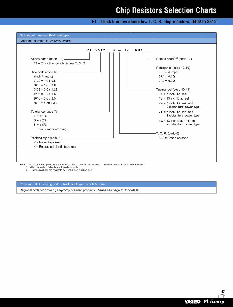
47
Chip Resistors Selection ChartsPT - Thick film low ohmic low T. C. R. chip resistors, 0402 to 2512
Global part number - Preferred type
Ordering example: PT2512FK-070R01L
P T 2 5 1 2 F K ― 0 7 0 R 0 1 L
Series name (code 1-2) Default code(1/2) (code 17)PT = Thick film low ohmic low T. C. R. Resistance (code 12-16)
Size code (code 3-6) 0R = Jumper (inch / metric) 0R1 = 0.1Ω0402 = 1.0 x 0.5 0R2 = 0.2Ω0603 = 1.6 x 0.8 0805 = 2.0 x 1.25 Taping reel (code 10-11)1206 = 3.2 x 1.6 07 = 7 inch Dia. reel2010 = 5.0 x 2.5 13 = 13 inch Dia. reel2512 = 6.35 x 3.2 7W = 7 inch Dia. reel and
2 x standard power typeTolerance (code 7) 7T = 7 inch Dia. reel and
3 x standard power type F = ± 1% G = ± 2% 3W = 13 inch Dia. reel and
2 x standard power typeJ = ± 5% “―” for Jumper ordering T. C. R. (code 9)
Packing style (code 8 ) “―” = Based on spec.R = Paper tape reelK = Embossed plastic tape reel
Note: 1. All of our RSMD products are RoHS compliant. "LFP" of the internal 2D reel label mentions "Lead Free Process" 2. Letter L is system default code for ordering only 3. PT series products are available by "Global part number" only
Phycomp CTC ordering code - Traditional type - North America
Regional code for ordering Phycomp branded products. Please see page 15 for details.
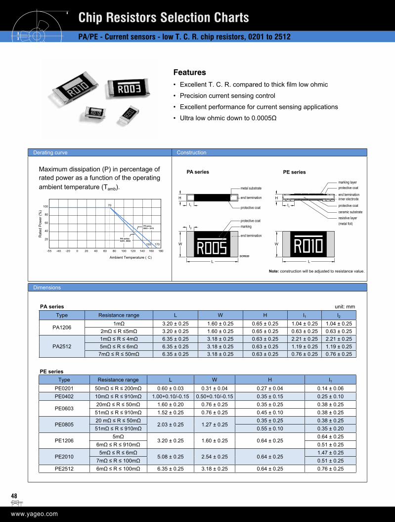
48
Derating curve Construction
Maximum dissipation (P) in percentage of rated power as a function of the operating ambient temperature (Tamb).
100
80
60
40
20
-55 -40 -20 0 20 40 60 80
70
100 120 140 160 180
Ambient Temperature ( C)
Rat
ed P
ower
(%)
155 170
PA series 0201, 0402
PE series0603 ~ 2512
Dimensions
PA series unit: mmType Resistance range L W H l1 l2
PA12061mΩ 3.20 ± 0.25 1.60 ± 0.25 0.65 ± 0.25 1.04 ± 0.25 1.04 ± 0.25
2mΩ ≤ R ≤5mΩ 3.20 ± 0.25 1.60 ± 0.25 0.65 ± 0.25 0.63 ± 0.25 0.63 ± 0.25
PA25121mΩ ≤ R ≤ 4mΩ 6.35 ± 0.25 3.18 ± 0.25 0.63 ± 0.25 2.21 ± 0.25 2.21 ± 0.255mΩ ≤ R ≤ 6mΩ 6.35 ± 0.25 3.18 ± 0.25 0.63 ± 0.25 1.19 ± 0.25 1.19 ± 0.25
7mΩ ≤ R ≤ 50mΩ 6.35 ± 0.25 3.18 ± 0.25 0.63 ± 0.25 0.76 ± 0.25 0.76 ± 0.25
PE seriesType Resistance range L W H l1
PE0201 50mΩ ≤ R ≤ 200mΩ 0.60 ± 0.03 0.31 ± 0.04 0.27 ± 0.04 0.14 ± 0.06PE0402 10mΩ ≤ R ≤ 910mΩ 1.00+0.10/-0.15 0.50+0.10/-0.15 0.35 ± 0.15 0.25 ± 0.10
PE060320mΩ ≤ R ≤ 50mΩ 1.60 ± 0.20 0.76 ± 0.25 0.35 ± 0.25 0.38 ± 0.2551mΩ ≤ R ≤ 910mΩ 1.52 ± 0.25 0.76 ± 0.25 0.45 ± 0.10 0.38 ± 0.25
PE080520 mΩ ≤ R ≤ 50mΩ
2.03 ± 0.25 1.27 ± 0.250.35 ± 0.25 0.38 ± 0.25
51mΩ ≤ R ≤ 910mΩ 0.55 ± 0.10 0.35 ± 0.20
PE12065mΩ
3.20 ± 0.25 1.60 ± 0.25 0.64 ± 0.250.64 ± 0.25
6mΩ ≤ R ≤ 910mΩ 0.51 ± 0.25
PE20105mΩ ≤ R ≤ 6mΩ
5.08 ± 0.25 2.54 ± 0.25 0.64 ± 0.251.47 ± 0.25
7mΩ ≤ R ≤ 100mΩ 0.51 ± 0.25PE2512 6mΩ ≤ R ≤ 100mΩ 6.35 ± 0.25 3.18 ± 0.25 0.64 ± 0.25 0.76 ± 0.25
Chip Resistors Selection ChartsPA/PE - Current sensors - low T. C. R. chip resistors, 0201 to 2512
PA series
SCR020
Features• Excellent T. C. R. compared to thick film low ohmic
• Precision current sensing control
• Excellent performance for current sensing applications
• Ultra low ohmic down to 0.0005Ω
Note: construction will be adjusted to resistance value.
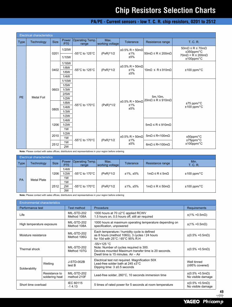
49
Electrical characteristics
Type Technology Size Power P70
Operating Temp. range
Max. working voltage Tolerance Resistance range T. C. R.
PE Metal Foil
02011/20W
-55°C to 125°C (PxR)^1/2±0.5% R > 50mΩ
±1%±5%
50mΩ ≤ R ≤ 200mΩ
50mΩ ≤ R ≤ 70mΩ±350ppm/°C
70mΩ < R ≤ 200mΩ±100ppm/°C1/10W
0402
1/16W
-55°C to 125°C (PxR)^1/2±0.5% R > 50mΩ
±1%±5%
10mΩ ≤ R ≤ 910mΩ ±100 ppm/°C1/8W1/6W1/4W
0603
1/10W
-55°C to 170°C (PxR)^1/2±0.5% R > 50mΩ
±1%±5%
5m,10m,20mΩ ≤ R ≤ 910mΩ
±75 ppm/°C±100 ppm/°C
1/5W1/3W2/5W1/2W
0805
1/8W1/4W1/3W1/2W
12061/4W
5mΩ ≤ R ≤ 910mΩ 1/2W1W
20101/2W
-55°C to 170°C (PxR)^1/2±0.5% R > 50mΩ
±1%±5%
5mΩ ≤ R<100mΩ ±50ppm/°C±75ppm/°C±100ppm/°C
1W
25121W
6mΩ ≤ R<100mΩ2W
Note: Please contact with sales offices, distributors and representatives in your region before ordering Electrical characteristics
Type Technology Size Power P70
Operating Temp. range
Max. working voltage Tolerance Resistance range Min.
T. C. R.
PA Metal Plate
12061/4W
-55°C to 170°C (PxR)^1/2 ±1%, ±5% 1mΩ ≤ R ≤ 5mΩ ±100 ppm/°C1/2W1W
25121W
-55°C to 170°C (PxR)^1/2 ±1%, ±5% 1mΩ ≤ R ≤ 50mΩ ±100 ppm/°C 2W3W
Note: Please contact with sales offices, distributors and representatives in your region before ordering
Environmental characteristics
Performance test Test method Procedure Requirements
Life MIL-STD-202 Method 108A
1000 hours at 70 ±2°C applied RCWV 1.5 hours on, 0.5 hours off, still air required ±(1% +0.5mΩ)
High temperature exposure MIL-STD-202 Method 108A
1000 hours at maximum operating temperature depending on specification, unpowered ±(1% +0.5mΩ)
Moisture resistance MIL-STD-202 Method 106G
Each temperature / humidity cycle is defined as 8 hours (method 106G), 3 cycles / 24 hours for 10d with 25°C / 65°C 95% R.H
±(0.5% +0.5mΩ)
Thermal shock MIL-STD-202 Method 107G
-55/+125 °CNote: Number of cycles required is 300. Devices mounted Maximum transfer time is 20 seconds. Dwell time is 15 minutes. Air – Air
±(0.5% +0.5mΩ)
Solderability Wetting J-STD-002B
test B
Electrical test not required. Magnification 50X Lead-free solder bath at 245 ±3°C Dipping time: 3 ±0.5 seconds
Well tinned (≥95% covered)
Resistance to soldering heat
MIL-STD-202 method 210F Lead-free solder, 260°C, 10 seconds immersion time ±(0.5% +0.5mΩ)
No visible damage
Short time overload IEC 60115-1 4.13 5 times of rated power for 5 seconds at room temperature ±(0.5% +0.5mΩ)
No visible damage
Chip Resistors Selection ChartsPA/PE - Current sensors - low T. C. R. chip resistors, 0201 to 2512
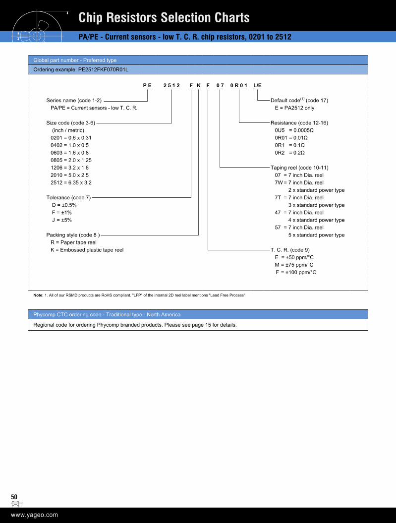
50
Global part number - Preferred type
Ordering example: PE2512FKF070R01L
P E 2 5 1 2 F K F 0 7 0 R 0 1 L/E
Series name (code 1-2) Default code(1) (code 17)PA/PE = Current sensors - low T. C. R. E = PA2512 only
Size code (code 3-6) Resistance (code 12-16) (inch / metric) 0U5 = 0.0005Ω0201 = 0.6 x 0.31 0R01 = 0.01Ω0402 = 1.0 x 0.5 0R1 = 0.1Ω0603 = 1.6 x 0.8 0R2 = 0.2Ω0805 = 2.0 x 1.251206 = 3.2 x 1.6 Taping reel (code 10-11)2010 = 5.0 x 2.5 07 = 7 inch Dia. reel2512 = 6.35 x 3.2 7W = 7 inch Dia. reel
2 x standard power typeTolerance (code 7) 7T = 7 inch Dia. reel
D = ±0.5% 3 x standard power type F = ±1% 47 = 7 inch Dia. reel J = ±5% 4 x standard power type
57 = 7 inch Dia. reelPacking style (code 8 ) 5 x standard power type
R = Paper tape reelK = Embossed plastic tape reel T. C. R. (code 9)
E = ±50 ppm/°CM = ±75 ppm/°C F = ±100 ppm/°C
Note: 1. All of our RSMD products are RoHS compliant. "LFP" of the internal 2D reel label mentions "Lead Free Process"
Phycomp CTC ordering code - Traditional type - North America
Regional code for ordering Phycomp branded products. Please see page 15 for details.
Chip Resistors Selection ChartsPA/PE - Current sensors - low T. C. R. chip resistors, 0201 to 2512
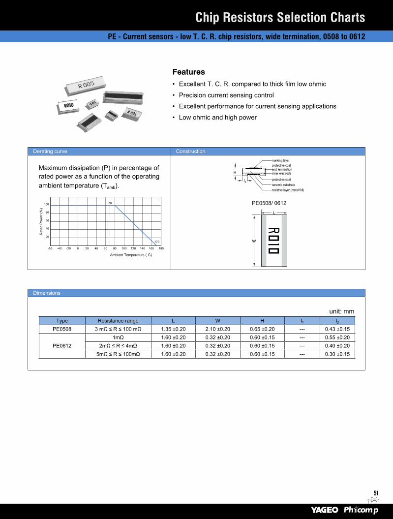
51
Derating curve Construction
Maximum dissipation (P) in percentage of rated power as a function of the operating ambient temperature (Tamb).
100
80
60
40
20
-55 -40 -20 0 20 40 60 80
70
100 120 140 160 180
Ambient Temperature ( C)
Rat
ed P
ower
(%)
170
Dimensions
unit: mmType Resistance range L W H l1 l2
PE0508 3 mΩ ≤ R ≤ 100 mΩ 1.35 ±0.20 2.10 ±0.20 0.65 ±0.20 --- 0.43 ±0.15
PE06121mΩ 1.60 ±0.20 0.32 ±0.20 0.60 ±0.15 --- 0.55 ±0.20
2mΩ ≤ R ≤ 4mΩ 1.60 ±0.20 0.32 ±0.20 0.60 ±0.15 --- 0.40 ±0.205mΩ ≤ R ≤ 100mΩ 1.60 ±0.20 0.32 ±0.20 0.60 ±0.15 --- 0.30 ±0.15
PE0508/ 0612
Chip Resistors Selection ChartsPE - Current sensors - low T. C. R. chip resistors, wide termination, 0508 to 0612
Features• Excellent T. C. R. compared to thick film low ohmic
• Precision current sensing control
• Excellent performance for current sensing applications
• Low ohmic and high power
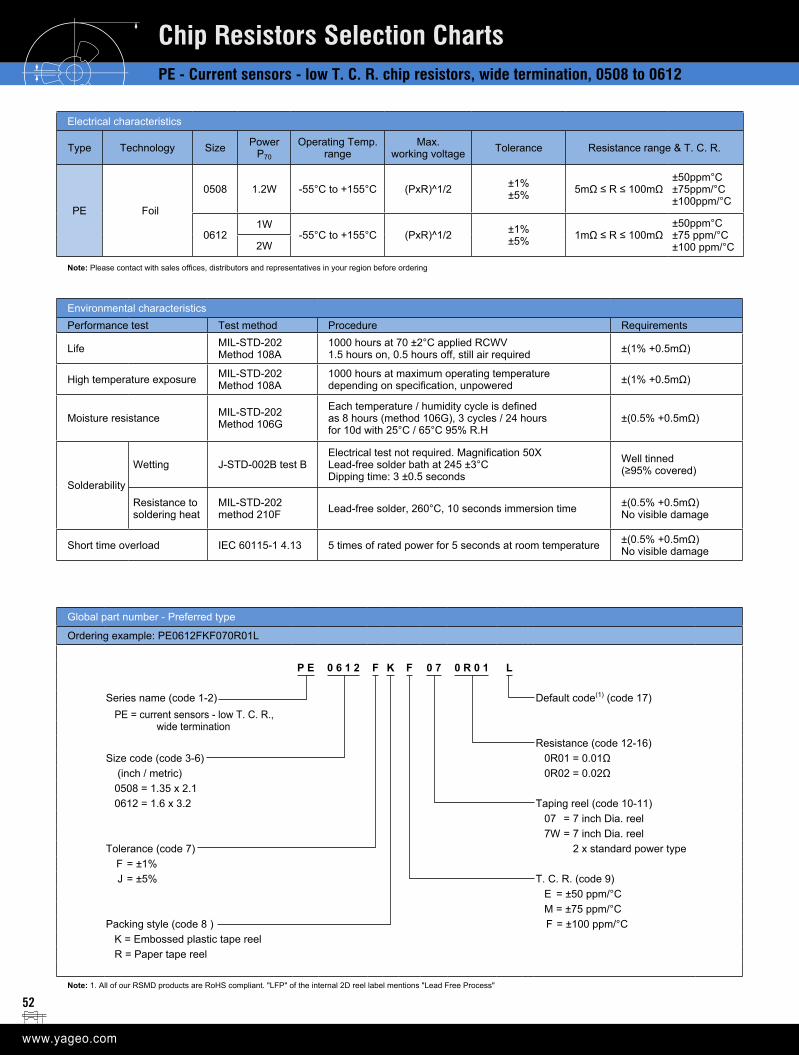
52
Electrical characteristics
Type Technology Size Power P70
Operating Temp. range
Max. working voltage Tolerance Resistance range & T. C. R.
PE Foil
0508 1.2W -55°C to +155°C (PxR)^1/2 ±1% ±5% 5mΩ ≤ R ≤ 100mΩ
±50ppm°C ±75ppm/°C ±100ppm/°C
06121W
-55°C to +155°C (PxR)^1/2 ±1%±5% 1mΩ ≤ R ≤ 100mΩ
±50ppm°C ±75 ppm/°C±100 ppm/°C2W
Note: Please contact with sales offices, distributors and representatives in your region before ordering
Environmental characteristics Performance test Test method Procedure Requirements
Life MIL-STD-202 Method 108A
1000 hours at 70 ±2°C applied RCWV 1.5 hours on, 0.5 hours off, still air required ±(1% +0.5mΩ)
High temperature exposure MIL-STD-202 Method 108A
1000 hours at maximum operating temperature depending on specification, unpowered ±(1% +0.5mΩ)
Moisture resistance MIL-STD-202 Method 106G
Each temperature / humidity cycle is definedas 8 hours (method 106G), 3 cycles / 24 hours for 10d with 25°C / 65°C 95% R.H
±(0.5% +0.5mΩ)
Solderability
Wetting J-STD-002B test BElectrical test not required. Magnification 50X Lead-free solder bath at 245 ±3°C Dipping time: 3 ±0.5 seconds
Well tinned (≥95% covered)
Resistance to soldering heat
MIL-STD-202 method 210F Lead-free solder, 260°C, 10 seconds immersion time ±(0.5% +0.5mΩ)
No visible damage
Short time overload IEC 60115-1 4.13 5 times of rated power for 5 seconds at room temperature ±(0.5% +0.5mΩ)No visible damage
Chip Resistors Selection ChartsPE - Current sensors - low T. C. R. chip resistors, wide termination, 0508 to 0612
Global part number - Preferred type
Ordering example: PE0612FKF070R01L
P E 0 6 1 2 F K F 0 7 0 R 0 1 L
Series name (code 1-2) Default code(1) (code 17)PE = current sensors - low T. C. R., wide termination Resistance (code 12-16)
Size code (code 3-6) 0R01 = 0.01Ω (inch / metric) 0R02 = 0.02Ω0508 = 1.35 x 2.10612 = 1.6 x 3.2 Taping reel (code 10-11)
07 = 7 inch Dia. reel7W = 7 inch Dia. reel
Tolerance (code 7) 2 x standard power type F = ±1% J = ±5% T. C. R. (code 9) E = ±50 ppm/°C
M = ±75 ppm/°CPacking style (code 8 ) F = ±100 ppm/°C
K = Embossed plastic tape reelR = Paper tape reel
Note: 1. All of our RSMD products are RoHS compliant. "LFP" of the internal 2D reel label mentions "Lead Free Process"
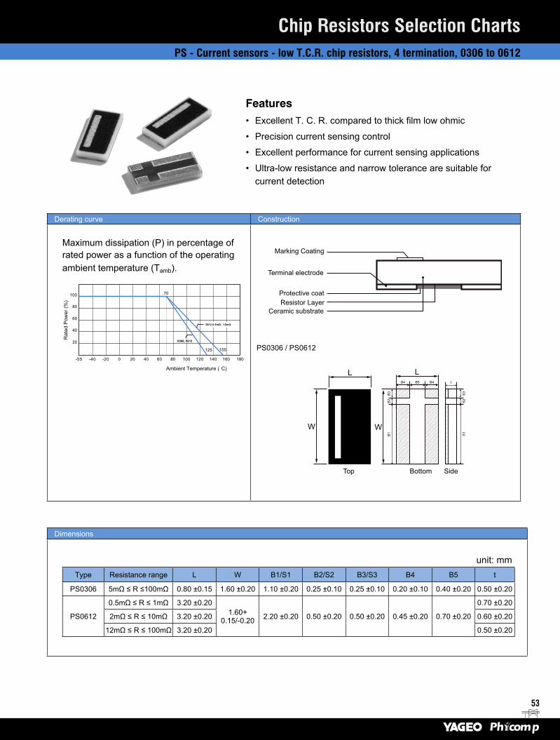
53
Derating curve Construction
Maximum dissipation (P) in percentage of rated power as a function of the operating ambient temperature (Tamb).
100
80
60
40
20
-55 -40 -20 0 20 40 60 80
70
100 120 140 160 180
Ambient Temperature ( C)
Rat
ed P
ower
(%)
155
0306, 0612
0612 0.5mΩ - 10mΩ
125
Dimensions
unit: mmType Resistance range L W B1/S1 B2/S2 B3/S3 B4 B5 t
PS0306 5mΩ ≤ R ≤100mΩ 0.80 ±0.15 1.60 ±0.20 1.10 ±0.20 0.25 ±0.10 0.25 ±0.10 0.20 ±0.10 0.40 ±0.20 0.50 ±0.20
PS0612
0.5mΩ ≤ R ≤ 1mΩ 3.20 ±0.201.60+
0.15/-0.20 2.20 ±0.20 0.50 ±0.20 0.50 ±0.20 0.45 ±0.20 0.70 ±0.20
0.70 ±0.20
2mΩ ≤ R ≤ 10mΩ 3.20 ±0.20 0.60 ±0.20
12mΩ ≤ R ≤ 100mΩ 3.20 ±0.20 0.50 ±0.20
Chip Resistors Selection ChartsPS - Current sensors - low T.C.R. chip resistors, 4 termination, 0306 to 0612
Features• Excellent T. C. R. compared to thick film low ohmic
• Precision current sensing control
• Excellent performance for current sensing applications
• Ultra-low resistance and narrow tolerance are suitable for current detection
PS0306 / PS0612
Marking Coating
Terminal electrode
Protective coatResistor Layer
Ceramic substrate
Bottom Side
L
Top
L
W W
B4 B4 tB5
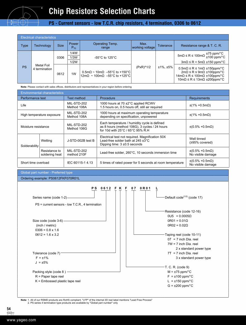
54
Electrical characteristics
Type Technology Size Power P70
Operating Temp. range
Max. working voltage Tolerance Resistance range & T. C. R.
PS Metal Foil4 termination
03061/4W
-55°C to 125°C
(PxR)^1/2 ±1%, ±5%
±75 ppm/°C±100 ppm/°C1/3W
1/2W 3mΩ ≤ R < 5mΩ ±150 ppm/°C
0612 1W 0.5mΩ ~ 10mΩ –55°C to +150°C12mΩ ~ 100mΩ –55°C to +125°C
0.5mΩ ≤ R ≤ 1mΩ2mΩ ≤ R ≤ 9mΩ
14mΩ ≤ R ≤ 100mΩ10mΩ ≤ R ≤ 13mΩ
±150ppm/°C±100ppm/°C±100ppm/°C±200ppm/°C
Note: Please contact with sales offices, distributors and representatives in your region before ordering
Environmental characteristics Performance test Test method Procedure Requirements
Life MIL-STD-202 Method 108A
1000 hours at 70 ±2°C applied RCWV 1.5 hours on, 0.5 hours off, still air required ±(1% +0.5mΩ)
High temperature exposure MIL-STD-202 Method 108A
1000 hours at maximum operating temperature depending on specification, unpowered ±(1% +0.5mΩ)
Moisture resistance MIL-STD-202 Method 106G
Each temperature / humidity cycle is defined as 8 hours (method 106G), 3 cycles / 24 hours for 10d with 25°C / 65°C 95% R.H
±(0.5% +0.5mΩ)
Solderability Wetting J-STD-002B test B
Electrical test not required. Magnification 50X Lead-free solder bath at 245 ±3°C Dipping time: 3 ±0.5 seconds
Well tinned (≥95% covered)
Resistance to soldering heat
MIL-STD-202 method 210F Lead-free solder, 260°C, 10 seconds immersion time ±(0.5% +0.5mΩ)
No visible damage
Short time overload IEC 60115-1 4.13 5 times of rated power for 5 seconds at room temperature ±(0.5% +0.5mΩ)No visible damage
Chip Resistors Selection ChartsPS - Current sensors - low T.C.R. chip resistors, 4 termination, 0306 to 0612
Global part number - Preferred type
Ordering example: PS0612FKF070R01L
P S 0 6 1 2 F K F 0 7 0 R 0 1 L
Series name (code 1-2) Default code(1/2) (code 17)
PS = current sensors - low T.C.R., 4 termination
Resistance (code 12-16)0U5 = 0.0005Ω
Size code (code 3-6) 0R01 = 0.01Ω (inch / metric) 0R02 = 0.02Ω0306 = 0.8 x 1.60612 = 1.6 x 3.2 Taping reel (code 10-11)
07 = 7 inch Dia. reel7W = 7 inch Dia. reel 2 x standard power type
Tolerance (code 7) 7T = 7 inch Dia. reel F = ±1% 3 x standard power typeJ = ±5%
T. C. R. (code 9)Packing style (code 8 ) M = ±75 ppm/°C
R = Paper tape reel F = ±100 ppm/°C K = Embossed plastic tape reel L = ±150 ppm/°C
G = ±200 ppm/°C
Note: 1. All of our RSMD products are RoHS compliant. "LFP" of the internal 2D reel label mentions "Lead Free Process" 2. PS series 4 termination type products are available by "Global part number" only
5mΩ ≤ R ≤ 100mΩ
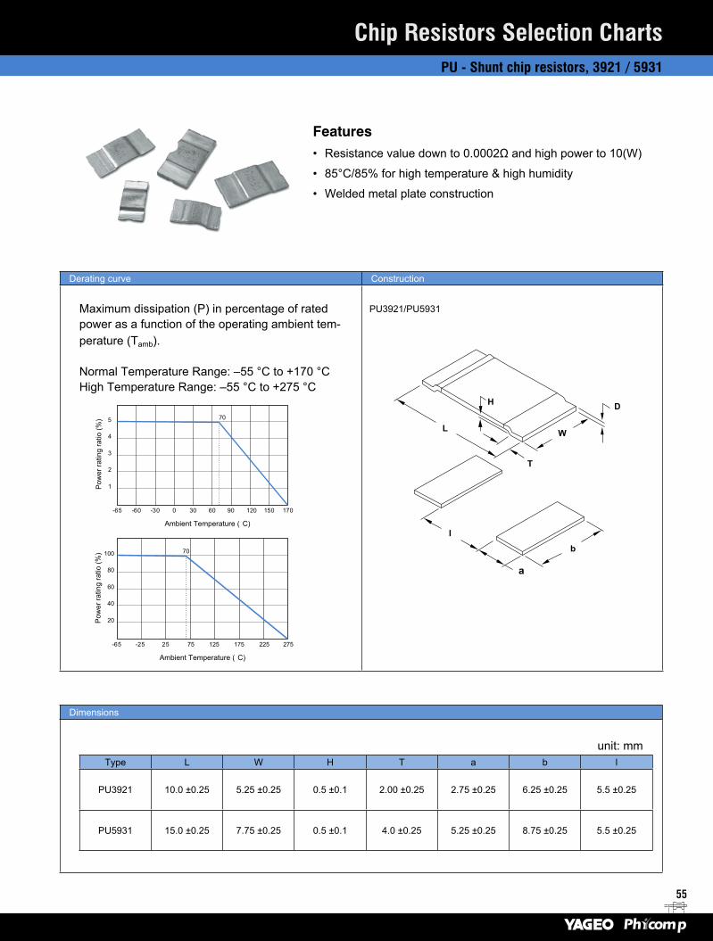
55
Derating curve Construction
Maximum dissipation (P) in percentage of rated power as a function of the operating ambient tem-perature (Tamb).
Normal Temperature Range: –55 °C to +170 °C High Temperature Range: –55 °C to +275 °C
5
4
3
2
1
-65 -60 -30 0 30 60 90 120
70
150 170
Ambient Temperature ( C)
Pow
er ra
ting
ratio
(%)
Dimensions
unit: mmType L W H T a b l
PU3921 10.0 ±0.25 5.25 ±0.25 0.5 ±0.1 2.00 ±0.25 2.75 ±0.25 6.25 ±0.25 5.5 ±0.25
PU5931 15.0 ±0.25 7.75 ±0.25 0.5 ±0.1 4.0 ±0.25 5.25 ±0.25 8.75 ±0.25 5.5 ±0.25
Features• Resistance value down to 0.0002Ω and high power to 10(W)
• 85°C/85% for high temperature & high humidity
• Welded metal plate construction
PU3921/PU5931
D
T
b
a
I
H
L W
Chip Resistors Selection ChartsPU - Shunt chip resistors, 3921 / 5931
100
80
60
40
20
-65 -25 25 75 125 175 225 275
70
Ambient Temperature ( C)
Pow
er ra
ting
ratio
(%)
56
Electrical characteristics
Type Size Power P70
Max voltage Operating Temp. range Resistance range Tolerance TCR
PU
39213W
(PxR)^1/2
-55°C to 170°C 0.2mR/ 0.3mR/ 0.5mR/ 1mR/ 2mR/3mR/4mR
±1%,±5%0.2mR
0.3mR/ 0.5mR1mR~4mR
±325ppm/°C±175ppm/°C±75ppm/°C
-55°C to 275°C 0.5mR/1mR/ 2mR/3mR/4mR5W
-55°C to 170°C2mR/3mR/4mR
9W 0.2mR/ 0.3mR/ 0.5mR/1mR
59315W
-55°C to 170°C 0.2mR/ 0.3mR/ 0.5mR/1mR/ 2mR/3mR/4mR
±1%,±5%0.2mR
0.3mR/ 0.5mR1mR~4mR
±225ppm/°C±175ppm/°C±75ppm/°C
-55°C to 275°C 0.3mR/0.5mR/1mR/2mR/3mR/4mR7W
-55°C to 170°C1mR/2mR/3mR/4mR
10W 0.2mR/ 0.3mR/ 0.5mRNote: Please contact with sales offices, distributors and representatives in your region before ordering
Environmental characteristics Performance test Test method Procedure Requirements
Life MIL-STD-202 Method 108A
1000 hours at 70 ±2°C applied RCWV 1.5 hours on, 0.5 hours off, still air required ±(1% +0.5mΩ)
High temperature exposure MIL-STD-202 Method 108A
1000 hours at maximum operating temperature depending on specification, unpowered ±(1% +0.5mΩ)
Moisture resistance MIL-STD-202 Method 106G
Each temperature / humidity cycle is defined as 8 hours (method 106G), 3 cycles / 24 hoursfor 10d with 25°C / 65°C 95% R.H
±(0.5% +0.5mΩ)
Solderability Resistance to soldering heat
MIL-STD-202 method 210F Lead-free solder, 260°C, 10 seconds immersion time ±(0.5% +0.5mΩ)
No visible damage
Short time overload IEC 60115-1 4.13 5 times of rated power for 5 seconds at room temperature ±(0.5% +0.5mΩ)No visible damage
Chip Resistors Selection ChartsPU - Shunt chip resistors, 3921 / 5931
Global part number - Preferred type
Ordering example: PU3921FKO130U2L
P U 3 9 2 1 F K O 1 3 0 U 2 L
Series name (code 1-2) Default code(1/2) (code 17)
PU = Metal shunt resistor
Resistance (code 12-16)0R005 = 0.005Ω
Size code (code 3-6) 0U2 = 0.0002Ω (inch / metric) 3921 = 10.0 x 5.2 Taping reel (code 10-11)5931 = 15.0 x 7.75 13 = Standard power, 13 inch Dia. reel
P5 = 5W , 13 inch Dia. reelP7 = 7W, 13 inch Dia. reel
Tolerance (code 7) P9 = 9W , 13 inch Dia. reel F = ±1% T3 = 3W , High temperature 13 inch Dia. reelJ = ±5% T5 = 5W , High temperature 13 inch Dia. reel
PA = 10W, 13 inch Dia. reel
Packing style (code 8 ) T. C. R. (code 9)K = Embossed plastic tape reel M = ±75 ppm/°C
N = ±175 ppm/°CH = ±225 ppm/°CO = ±325 ppm/°C
Note: 1. All of our RSMD products are RoHS compliant. "LFP" of the internal 2D reel label mentions "Lead Free Process" 2. PU series 4 termination type products are available by "Global part number" only
57
Derating curve Construction
Maximum dissipation (P) in percentage of rated power as a function of the operating ambient temperature (Tamb).
100
80
60
40
20
-55 -40 -20 0 20 40 60 80
70
100 120 140 160
Ambient Temperature ( C)
Rat
ed P
ower
(%)
155
overcoat
protective glass
resistive layer(jumper chip is a conductor)
inner electrode
termination (Ni / Au / Pd)
ceramic substrate
marking layer
Dimensions
W
unit: mm
I2
I2
I1
I1
L
H
Type L W H I1 I2AR0402 1.00 ±0.05 0.50 ±0.05 0.35 ±0.05 0.20 ±0.10 0.25 ±0.10AR0603 1.60 ±0.10 0.80 ±0.10 0.45 ±0.10 0.25 ±0.15 0.25 ±0.15AR0805 2.00 ±0.10 1.25 ±0.10 0.50 ±0.10 0.35 ±0.20 0.35 ±0.20AR1206 3.10 ±0.10 1.60 ±0.10 0.55 ±0.10 0.45 ±0.20 0.40 ±0.20
Features• New NiAu terminations provide special application for
hybrid board gluing
• Competitive with NiAu terminations
• Special use in high temperature environment
• Higher component and equipment reliability
Chip Resistors Selection ChartsAR - NiAu termination chip resistors, 0402 to 1206
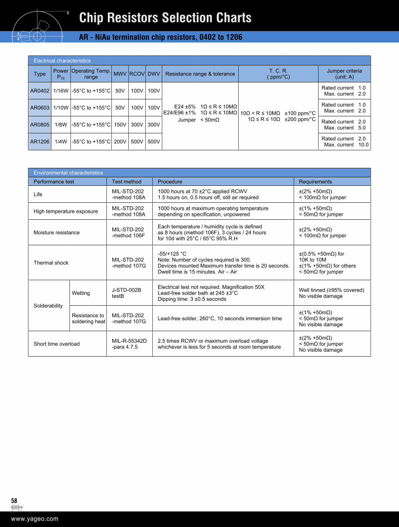
58
Electrical characteristics
Type Power P70
Operating Temp. range MWV RCOV DWV Resistance range & tolerance T. C. R.
( ppm/°C)Jumper criteria
(unit: A)
AR0402 1/16W -55°C to +155°C 50V 100V 100V
E24 ±5% E24/E96 ±1%
1Ω ≤ R ≤ 10MΩ1Ω ≤ R ≤ 10MΩ 10Ω < R ≤ 10MΩ
1Ω ≤ R ≤ 10Ω±100 ppm/°C ±200 ppm/°C
Rated current Max. current
1.0 2.0
AR0603 1/10W -55°C to +155°C 50V 100V 100V Rated current Max. current
1.0 2.0
AR0805 1/8W -55°C to +155°C 150V 300V 300VJumper < 50mΩ Rated current
Max. current 2.0 5.0
AR1206 1/4W -55°C to +155°C 200V 500V 500V Rated current Max. current
2.0 10.0
Environmental characteristics
Performance test Test method Procedure Requirements
Life MIL-STD-202 -method 108A
1000 hours at 70 ±2°C applied RCWV 1.5 hours on, 0.5 hours off, still air required
±(2% +50mΩ) < 100mΩ for jumper
High temperature exposure MIL-STD-202 -method 108A
1000 hours at maximum operating temperature depending on specification, unpowered
±(1% +50mΩ) < 50mΩ for jumper
Moisture resistance MIL-STD-202 -method 106F
Each temperature / humidity cycle is defined as 8 hours (method 106F), 3 cycles / 24 hours for 10d with 25°C / 65°C 95% R.H
±(2% +50mΩ) < 100mΩ for jumper
Thermal shock MIL-STD-202 -method 107G
-55/+125 °CNote: Number of cycles required is 300. Devices mounted Maximum transfer time is 20 seconds. Dwell time is 15 minutes. Air – Air
±(0.5% +50mΩ) for 10K to 10M±(1% +50mΩ) for others< 50mΩ for jumper
Solderability
Wetting J-STD-002B testB
Electrical test not required. Magnification 50X Lead-free solder bath at 245 ±3°C Dipping time: 3 ±0.5 seconds
Well tinned (≥95% covered)No visible damage
Resistance to soldering heat
MIL-STD-202 -method 107G Lead-free solder, 260°C, 10 seconds immersion time
±(1% +50mΩ) < 50mΩ for jumperNo visible damage
Short time overload MIL-R-55342D-para 4.7.5
2.5 times RCWV or maximum overload voltage whichever is less for 5 seconds at room temperature
±(2% +50mΩ) < 50mΩ for jumperNo visible damage
Chip Resistors Selection ChartsAR - NiAu termination chip resistors, 0402 to 1206
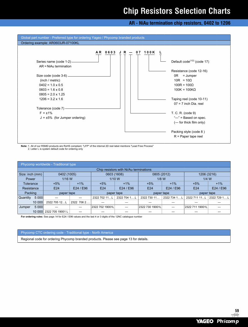
59
Global part number - Preferred type for ordering Yageo / Phycomp branded productsOrdering example: AR0603JR-07100KL
A R 0 6 0 3 J R ― 0 7 1 0 0 K L
Series name (code 1-2) Default code(1/2) (code 17) AR = NiAu termination
Resistance (code 12-16)Size code (code 3-6) 0R = Jumper
(inch / metric) 10R = 10Ω0402 = 1.0 x 0.5 100R = 100Ω0603 = 1.6 x 0.8 100K = 100KΩ0805 = 2.0 x 1.251206 = 3.2 x 1.6 Taping reel (code 10-11)
07 = 7 inch Dia. reelTolerance (code 7)
F = ±1% T. C. R. (code 9) J = ±5% (for Jumper ordering) “―” = Based on spec.
(― for thick film only)
Packing style (code 8 )R = Paper tape reel
Note: 1. All of our RSMD products are RoHS compliant. "LFP" of the internal 2D reel label mentions "Lead Free Process" 2. Letter L is system default code for ordering only
Phycomp worldwide - Traditional typeChip resistors with Ni/Au terminations
Size: inch (mm) 0402 (1005) 0603 (1608) 0805 (2012) 1206 (3216)Power 1/16 W 1/10 W 1/8 W 1/4 W
Tolerance +5% +1% +5% +1% +5% +1% +5% +1%Resistance E24 E24 / E96 E24 E24 / E96 E24 E24 / E96 E24 E24 / E96
Packing paper tape paper tape paper tape paper tapeQuantity 5 000 --- --- 2322 702 11…L 2322 704 1.…L 2322 730 11… 2322 734 1.…L 2322 711 11...L 2322 729 1.…L
10 000 2322 705 12…L 2322 706 2…. --- --- --- --- --- ---Jumper 5 000 --- --- 2322 702 19001L --- 2322 730 19001L --- 2322 711 19001L ---
10 000 2322 705 19001 L --- --- --- --- --- --- ---
For ordering rules: See page 14 for E24 / E96 values and the last 4 or 3 digits of the 12NC catalogue number
Phycomp CTC ordering code - Traditional type - North America
Regional code for ordering Phycomp branded products. Please see page 13 for details.
Chip Resistors Selection ChartsAR - NiAu termination chip resistors, 0402 to 1206
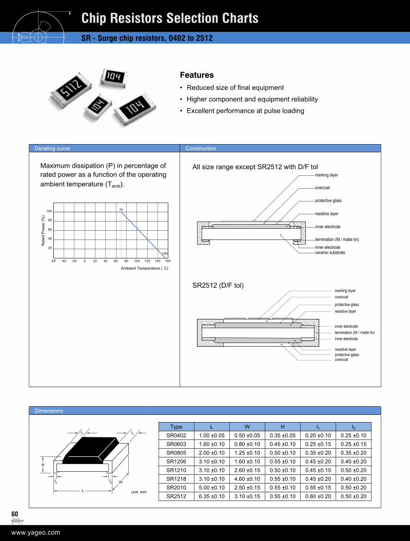
60
Derating curve Construction
Maximum dissipation (P) in percentage of rated power as a function of the operating ambient temperature (Tamb).
100
80
60
40
20
-55 -40 -20 0 20 40 60 80
70
100 120 140 160
Ambient Temperature ( C)
Rat
ed P
ower
(%)
155
Dimensions
W
unit: mm
I2
I2
I1
I1
L
H
Type L W H I1 I2SR0402 1.00 ±0.05 0.50 ±0.05 0.35 ±0.05 0.20 ±0.10 0.25 ±0.10SR0603 1.60 ±0.10 0.80 ±0.10 0.45 ±0.10 0.25 ±0.15 0.25 ±0.15SR0805 2.00 ±0.10 1.25 ±0.10 0.50 ±0.10 0.35 ±0.20 0.35 ±0.20SR1206 3.10 ±0.10 1.60 ±0.10 0.55 ±0.10 0.45 ±0.20 0.40 ±0.20SR1210 3.10 ±0.10 2.60 ±0.15 0.50 ±0.10 0.45 ±0.15 0.50 ±0.20SR1218 3.10 ±0.10 4.60 ±0.10 0.55 ±0.10 0.45 ±0.20 0.40 ±0.20SR2010 5.00 ±0.10 2.50 ±0.15 0.55 ±0.10 0.55 ±0.15 0.50 ±0.20SR2512 6.35 ±0.10 3.10 ±0.15 0.55 ±0.10 0.60 ±0.20 0.50 ±0.20
overcoat
protective glass
resistive layer
inner electrode
termination (Ni / matte tin)
ceramic substrateinner electrode
marking layer
overcoat
overcoat
protective glass
protective glass
resistive layer
resistive layer
inner electrodetermination (Ni / matte tin)inner electrode
marking layer
Features• Reduced size of final equipment
• Higher component and equipment reliability
• Excellent performance at pulse loading
Chip Resistors Selection ChartsSR - Surge chip resistors, 0402 to 2512
All size range except SR2512 with D/F tol
SR2512 (D/F tol)
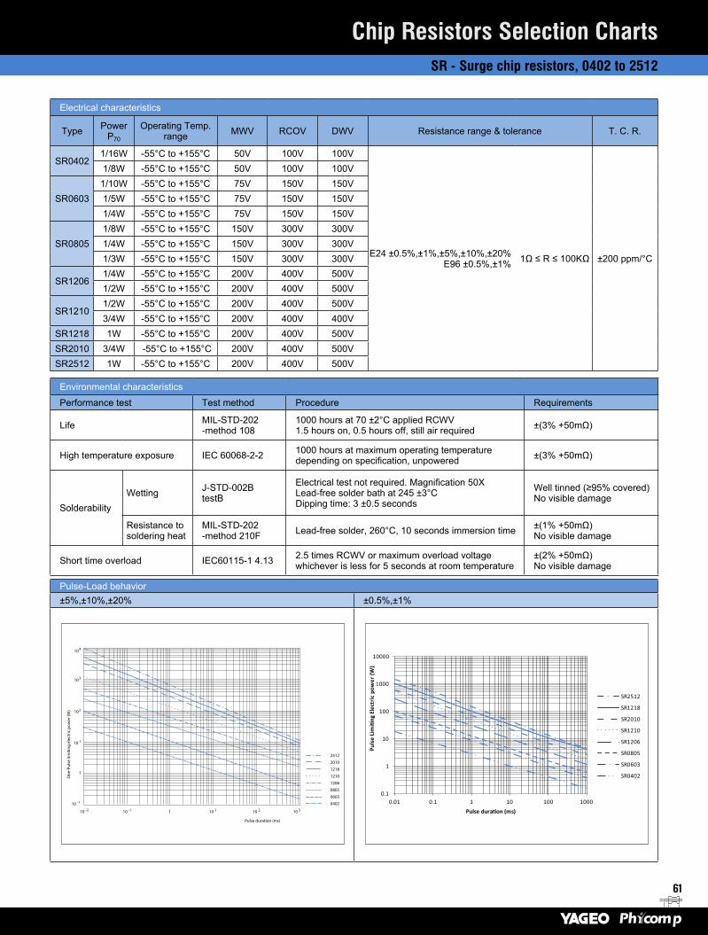
61
Electrical characteristics
Type Power P70
Operating Temp. range MWV RCOV DWV Resistance range & tolerance T. C. R.
SR04021/16W -55°C to +155°C 50V 100V 100V
E24 ±0.5%,±1%,±5%,±10%,±20%E96 ±0.5%,±1% 1Ω ≤ R ≤ 100KΩ ±200 ppm/°C
1/8W -55°C to +155°C 50V 100V 100V
SR06031/10W -55°C to +155°C 75V 150V 150V1/5W -55°C to +155°C 75V 150V 150V1/4W -55°C to +155°C 75V 150V 150V
SR08051/8W -55°C to +155°C 150V 300V 300V1/4W -55°C to +155°C 150V 300V 300V1/3W -55°C to +155°C 150V 300V 300V
SR12061/4W -55°C to +155°C 200V 400V 500V1/2W -55°C to +155°C 200V 400V 500V
SR12101/2W -55°C to +155°C 200V 400V 500V3/4W -55°C to +155°C 200V 400V 400V
SR1218 1W -55°C to +155°C 200V 400V 500VSR2010 3/4W -55°C to +155°C 200V 400V 500VSR2512 1W -55°C to +155°C 200V 400V 500V
Environmental characteristics
Performance test Test method Procedure Requirements
Life MIL-STD-202 -method 108
1000 hours at 70 ±2°C applied RCWV 1.5 hours on, 0.5 hours off, still air required ±(3% +50mΩ)
High temperature exposure IEC 60068-2-2 1000 hours at maximum operating temperature depending on specification, unpowered ±(3% +50mΩ)
Solderability Wetting J-STD-002B
testB
Electrical test not required. Magnification 50X Lead-free solder bath at 245 ±3°C Dipping time: 3 ±0.5 seconds
Well tinned (≥95% covered)No visible damage
Resistance to soldering heat
MIL-STD-202 -method 210F Lead-free solder, 260°C, 10 seconds immersion time ±(1% +50mΩ)
No visible damage
Short time overload IEC60115-1 4.13 2.5 times RCWV or maximum overload voltage whichever is less for 5 seconds at room temperature
±(2% +50mΩ)No visible damage
Pulse-Load behavior±5%,±10%,±20% ±0.5%,±1%
Chip Resistors Selection ChartsSR - Surge chip resistors, 0402 to 2512
103
104
1
102
1 10 1
10 1
10 2 10 310 -2 10 -1
10 -1
One
-Pul
se li
miti
ng e
lect
ric p
ower
(W)
Pulse duration (ms)
0805
0603
0402
1206
1218
1210
2010
2512
0.1
1
10
100
1000
10000
0.01 0.1 1 10 100 1000
Pulse
Lim
ing
Ele
ctric
pow
er (W
)
Pulse duraon (ms)
SR2512
SR1218
SR2010
SR1210
SR1206
SR0805
SR0603
SR0402
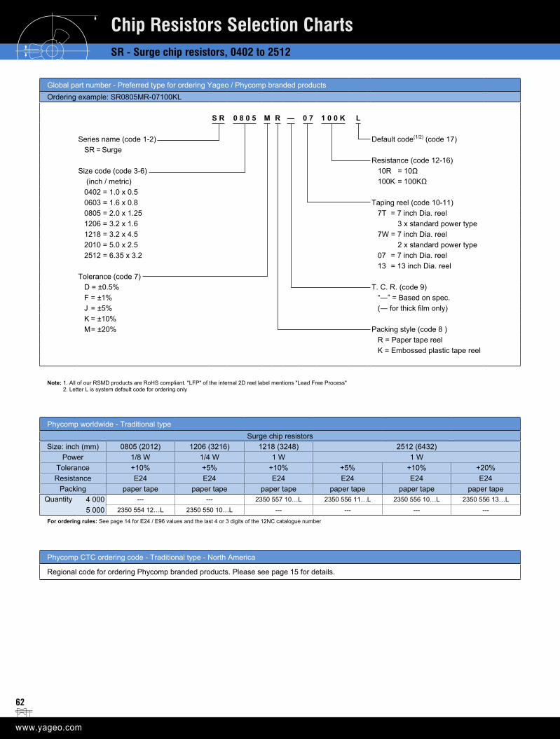
62
Global part number - Preferred type for ordering Yageo / Phycomp branded productsOrdering example: SR0805MR-07100KL
S R 0 8 0 5 M R ― 0 7 1 0 0 K L
Series name (code 1-2) Default code(1/2) (code 17) SR = Surge
Resistance (code 12-16)Size code (code 3-6) 10R = 10Ω
(inch / metric) 100K = 100KΩ0402 = 1.0 x 0.50603 = 1.6 x 0.8 Taping reel (code 10-11)0805 = 2.0 x 1.25 7T = 7 inch Dia. reel1206 = 3.2 x 1.6 3 x standard power type1218 = 3.2 x 4.5 7W = 7 inch Dia. reel2010 = 5.0 x 2.5 2 x standard power type2512 = 6.35 x 3.2 07 = 7 inch Dia. reel
13 = 13 inch Dia. reel Tolerance (code 7)
D = ±0.5% T. C. R. (code 9)F = ±1% “―” = Based on spec.J = ±5% (― for thick film only)K = ±10% M = ±20% Packing style (code 8 )
R = Paper tape reelK = Embossed plastic tape reel
Note: 1. All of our RSMD products are RoHS compliant. "LFP" of the internal 2D reel label mentions "Lead Free Process" 2. Letter L is system default code for ordering only
Phycomp worldwide - Traditional typeSurge chip resistors
Size: inch (mm) 0805 (2012) 1206 (3216) 1218 (3248) 2512 (6432)Power 1/8 W 1/4 W 1 W 1 W
Tolerance +10% +5% +10% +5% +10% +20%Resistance E24 E24 E24 E24 E24 E24
Packing paper tape paper tape paper tape paper tape paper tape paper tapeQuantity 4 000 --- --- 2350 557 10…L 2350 556 11…L 2350 556 10…L 2350 556 13…L
5 000 2350 554 12…L 2350 550 10…L --- --- --- ---
For ordering rules: See page 14 for E24 / E96 values and the last 4 or 3 digits of the 12NC catalogue number
Phycomp CTC ordering code - Traditional type - North America
Regional code for ordering Phycomp branded products. Please see page 15 for details.
Chip Resistors Selection ChartsSR - Surge chip resistors, 0402 to 2512
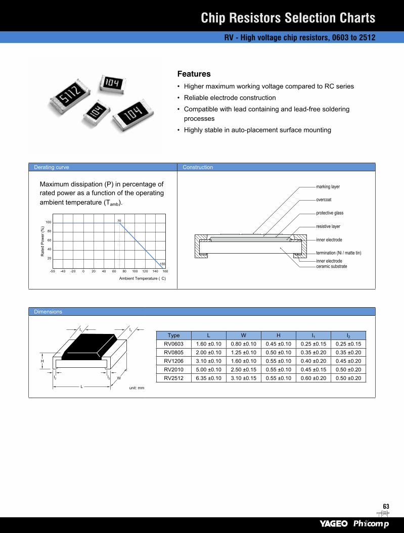
63
Derating curve Construction
Maximum dissipation (P) in percentage of rated power as a function of the operating ambient temperature (Tamb).
100
80
60
40
20
-55 -40 -20 0 20 40 60 80
70
100 120 140 160
Ambient Temperature ( C)
Rat
ed P
ower
(%)
155
Dimensions
W
unit: mm
I2
I2
I1
I1
L
H
Type L W H I1 I2RV0603 1.60 ±0.10 0.80 ±0.10 0.45 ±0.10 0.25 ±0.15 0.25 ±0.15RV0805 2.00 ±0.10 1.25 ±0.10 0.50 ±0.10 0.35 ±0.20 0.35 ±0.20RV1206 3.10 ±0.10 1.60 ±0.10 0.55 ±0.10 0.40 ±0.20 0.45 ±0.20RV2010 5.00 ±0.10 2.50 ±0.15 0.55 ±0.10 0.45 ±0.15 0.50 ±0.20RV2512 6.35 ±0.10 3.10 ±0.15 0.55 ±0.10 0.60 ±0.20 0.50 ±0.20
overcoat
protective glass
resistive layer
inner electrode
termination (Ni / matte tin)
ceramic substrateinner electrode
marking layer
Features• Higher maximum working voltage compared to RC series
• Reliable electrode construction
• Compatible with lead containing and lead-free soldering processes
• Highly stable in auto-placement surface mounting
Chip Resistors Selection ChartsRV - High voltage chip resistors, 0603 to 2512
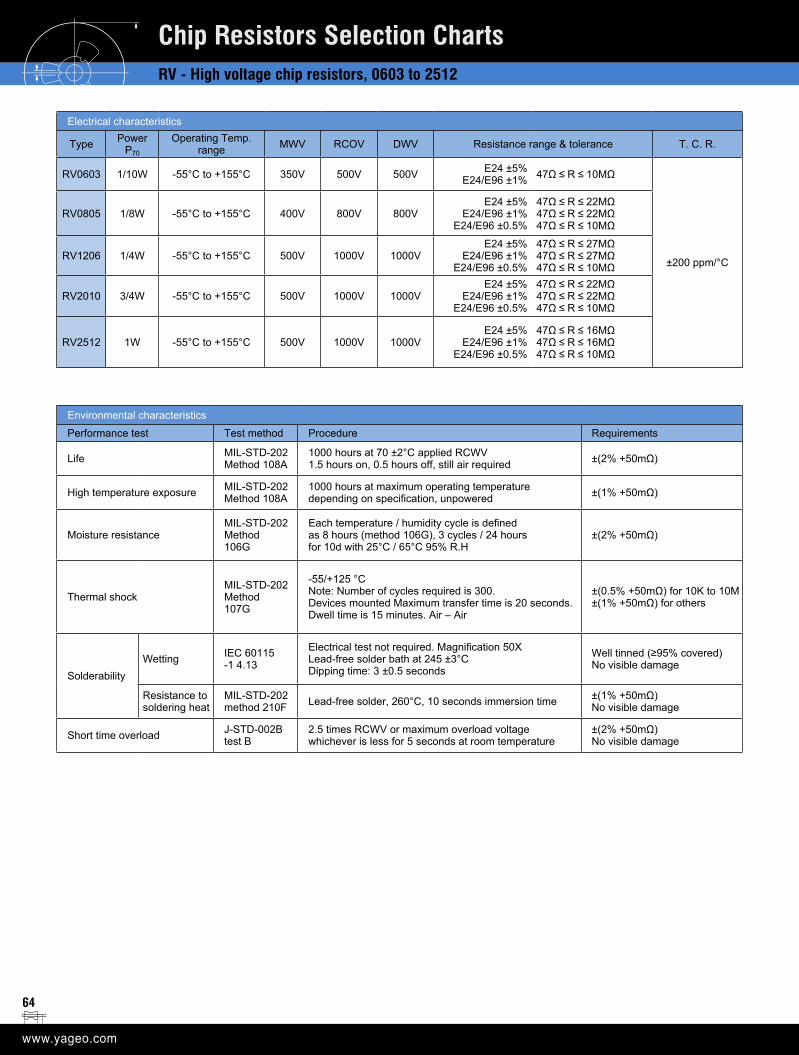
64
Electrical characteristics
Type Power P70
Operating Temp. range MWV RCOV DWV Resistance range & tolerance T. C. R.
RV0603 1/10W -55°C to +155°C 350V 500V 500V E24 ±5% E24/E96 ±1% 47Ω ≤ R ≤ 10MΩ
±200 ppm/°C
RV0805 1/8W -55°C to +155°C 400V 800V 800VE24 ±5%
E24/E96 ±1%E24/E96 ±0.5%
47Ω ≤ R ≤ 22MΩ47Ω ≤ R ≤ 22MΩ47Ω ≤ R ≤ 10MΩ
RV1206 1/4W -55°C to +155°C 500V 1000V 1000VE24 ±5%
E24/E96 ±1% E24/E96 ±0.5%
47Ω ≤ R ≤ 27MΩ 47Ω ≤ R ≤ 27MΩ 47Ω ≤ R ≤ 10MΩ
RV2010 3/4W -55°C to +155°C 500V 1000V 1000VE24 ±5%
E24/E96 ±1% E24/E96 ±0.5%
47Ω ≤ R ≤ 22MΩ 47Ω ≤ R ≤ 22MΩ 47Ω ≤ R ≤ 10MΩ
RV2512 1W -55°C to +155°C 500V 1000V 1000VE24 ±5%
E24/E96 ±1%E24/E96 ±0.5%
47Ω ≤ R ≤ 16MΩ47Ω ≤ R ≤ 16MΩ47Ω ≤ R ≤ 10MΩ
Environmental characteristics
Performance test Test method Procedure Requirements
Life MIL-STD-202 Method 108A
1000 hours at 70 ±2°C applied RCWV 1.5 hours on, 0.5 hours off, still air required ±(2% +50mΩ)
High temperature exposure MIL-STD-202 Method 108A
1000 hours at maximum operating temperature depending on specification, unpowered ±(1% +50mΩ)
Moisture resistanceMIL-STD-202 Method 106G
Each temperature / humidity cycle is definedas 8 hours (method 106G), 3 cycles / 24 hours for 10d with 25°C / 65°C 95% R.H
±(2% +50mΩ)
Thermal shockMIL-STD-202 Method 107G
-55/+125 °CNote: Number of cycles required is 300. Devices mounted Maximum transfer time is 20 seconds. Dwell time is 15 minutes. Air – Air
±(0.5% +50mΩ) for 10K to 10M ±(1% +50mΩ) for others
Solderability Wetting IEC 60115
-1 4.13
Electrical test not required. Magnification 50X Lead-free solder bath at 245 ±3°C Dipping time: 3 ±0.5 seconds
Well tinned (≥95% covered)No visible damage
Resistance to soldering heat
MIL-STD-202 method 210F Lead-free solder, 260°C, 10 seconds immersion time ±(1% +50mΩ)
No visible damage
Short time overload J-STD-002B test B
2.5 times RCWV or maximum overload voltage whichever is less for 5 seconds at room temperature
±(2% +50mΩ)No visible damage
Chip Resistors Selection ChartsRV - High voltage chip resistors, 0603 to 2512
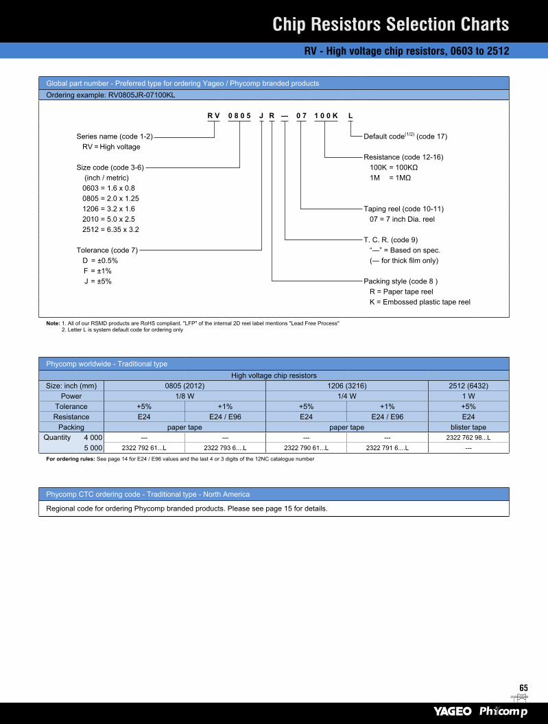
65
Global part number - Preferred type for ordering Yageo / Phycomp branded productsOrdering example: RV0805JR-07100KL
R V 0 8 0 5 J R ― 0 7 1 0 0 K L
Series name (code 1-2) Default code(1/2) (code 17) RV = High voltage
Resistance (code 12-16)Size code (code 3-6) 100K = 100KΩ
(inch / metric) 1M = 1MΩ0603 = 1.6 x 0.80805 = 2.0 x 1.251206 = 3.2 x 1.6 Taping reel (code 10-11)2010 = 5.0 x 2.5 07 = 7 inch Dia. reel2512 = 6.35 x 3.2
T. C. R. (code 9)Tolerance (code 7) “―” = Based on spec.
D = ±0.5% (― for thick film only) F = ±1% J = ±5% Packing style (code 8 )
R = Paper tape reelK = Embossed plastic tape reel
Note: 1. All of our RSMD products are RoHS compliant. "LFP" of the internal 2D reel label mentions "Lead Free Process" 2. Letter L is system default code for ordering only
Phycomp worldwide - Traditional typeHigh voltage chip resistors
Size: inch (mm) 0805 (2012) 1206 (3216) 2512 (6432)Power 1/8 W 1/4 W 1 W
Tolerance +5% +1% +5% +1% +5%Resistance E24 E24 / E96 E24 E24 / E96 E24
Packing paper tape paper tape blister tapeQuantity 4 000 --- --- --- --- 2322 762 98...L
5 000 2322 792 61...L 2322 793 6....L 2322 790 61...L 2322 791 6....L ---
For ordering rules: See page 14 for E24 / E96 values and the last 4 or 3 digits of the 12NC catalogue number
Phycomp CTC ordering code - Traditional type - North America
Regional code for ordering Phycomp branded products. Please see page 15 for details.
Chip Resistors Selection ChartsRV - High voltage chip resistors, 0603 to 2512
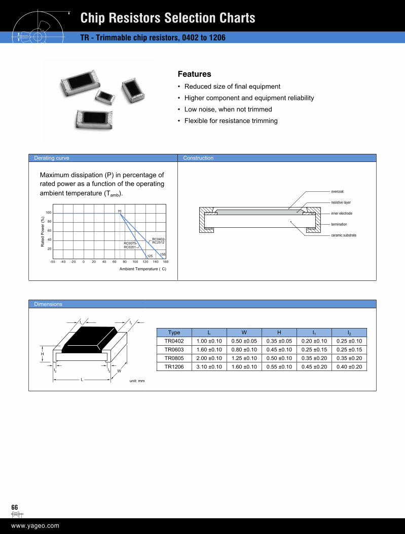
66
Derating curve Construction
Maximum dissipation (P) in percentage of rated power as a function of the operating ambient temperature (Tamb).
100
80
60
40
20
-55 -40 -20 0 20 40 60 80
70
100 120 140 160
Ambient Temperature ( C)
Rat
ed P
ower
(%)
155
RC0402-RC2512
125
RC0075-RC0201
overcoat
resistive layer
inner electrode
termination
ceramic substrate
Dimensions
W
unit: mm
I2
I2
I1
I1
L
H
Type L W H I1 I2TR0402 1.00 ±0.10 0.50 ±0.05 0.35 ±0.05 0.20 ±0.10 0.25 ±0.10TR0603 1.60 ±0.10 0.80 ±0.10 0.45 ±0.10 0.25 ±0.15 0.25 ±0.15TR0805 2.00 ±0.10 1.25 ±0.10 0.50 ±0.10 0.35 ±0.20 0.35 ±0.20TR1206 3.10 ±0.10 1.60 ±0.10 0.55 ±0.10 0.45 ±0.20 0.40 ±0.20
Features• Reduced size of final equipment
• Higher component and equipment reliability
• Low noise, when not trimmed
• Flexible for resistance trimming
Chip Resistors Selection ChartsTR - Trimmable chip resistors, 0402 to 1206
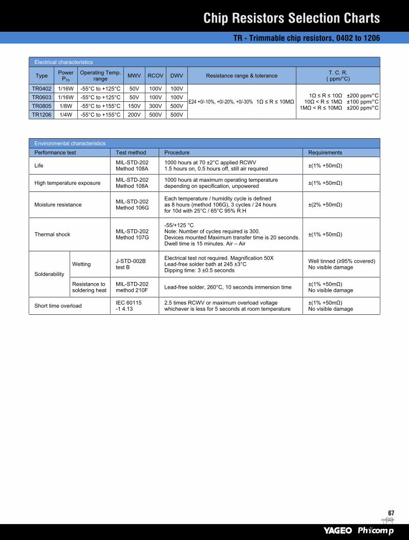
67
Electrical characteristics
Type Power P70
Operating Temp. range MWV RCOV DWV Resistance range & tolerance T. C. R.
( ppm/°C)
TR0402 1/16W -55°C to +125°C 50V 100V 100V
E24 +0/-10%, +0/-20%, +0/-30% 1Ω ≤ R ≤ 10MΩ1Ω ≤ R ≤ 10Ω
10Ω < R ≤ 1MΩ1MΩ < R ≤ 10MΩ
±200 ppm/°C±100 ppm/°C±200 ppm/°C
TR0603 1/16W -55°C to +125°C 50V 100V 100VTR0805 1/8W -55°C to +155°C 150V 300V 500VTR1206 1/4W -55°C to +155°C 200V 500V 500V
Environmental characteristics
Performance test Test method Procedure Requirements
Life MIL-STD-202 Method 108A
1000 hours at 70 ±2°C applied RCWV 1.5 hours on, 0.5 hours off, still air required ±(1% +50mΩ)
High temperature exposure MIL-STD-202 Method 108A
1000 hours at maximum operating temperature depending on specification, unpowered ±(1% +50mΩ)
Moisture resistance MIL-STD-202 Method 106G
Each temperature / humidity cycle is defined as 8 hours (method 106G), 3 cycles / 24 hours for 10d with 25°C / 65°C 95% R.H
±(2% +50mΩ)
Thermal shock MIL-STD-202 Method 107G
-55/+125 °CNote: Number of cycles required is 300. Devices mounted Maximum transfer time is 20 seconds. Dwell time is 15 minutes. Air – Air
±(1% +50mΩ)
Solderability
Wetting J-STD-002B test B
Electrical test not required. Magnification 50X Lead-free solder bath at 245 ±3°C Dipping time: 3 ±0.5 seconds
Well tinned (≥95% covered)No visible damage
Resistance to soldering heat
MIL-STD-202 method 210F Lead-free solder, 260°C, 10 seconds immersion time ±(1% +50mΩ)
No visible damage
Short time overload IEC 60115-1 4.13
2.5 times RCWV or maximum overload voltage whichever is less for 5 seconds at room temperature
±(1% +50mΩ)No visible damage
Chip Resistors Selection ChartsTR - Trimmable chip resistors, 0402 to 1206
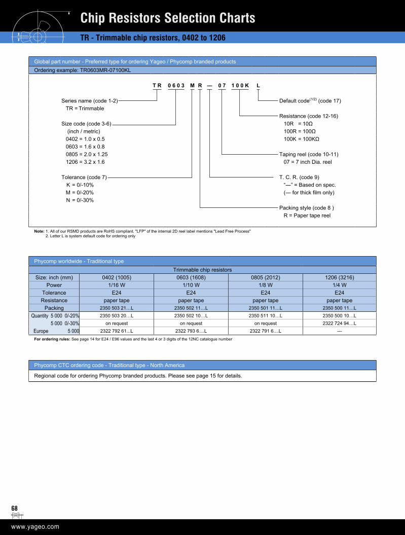
68
Global part number - Preferred type for ordering Yageo / Phycomp branded productsOrdering example: TR0603MR-07100KL
T R 0 6 0 3 M R ― 0 7 1 0 0 K L
Series name (code 1-2) Default code(1/2) (code 17) TR = Trimmable
Resistance (code 12-16)Size code (code 3-6) 10R = 10Ω
(inch / metric) 100R = 100Ω0402 = 1.0 x 0.5 100K = 100KΩ0603 = 1.6 x 0.80805 = 2.0 x 1.25 Taping reel (code 10-11)1206 = 3.2 x 1.6 07 = 7 inch Dia. reel
Tolerance (code 7) T. C. R. (code 9) K = 0/-10% “―” = Based on spec. M = 0/-20% (― for thick film only) N = 0/-30%
Packing style (code 8 )R = Paper tape reel
Note: 1. All of our RSMD products are RoHS compliant. "LFP" of the internal 2D reel label mentions "Lead Free Process" 2. Letter L is system default code for ordering only
Phycomp worldwide - Traditional typeTrimmable chip resistors
Size: inch (mm) 0402 (1005) 0603 (1608) 0805 (2012) 1206 (3216)Power 1/16 W 1/10 W 1/8 W 1/4 W
Tolerance E24 E24 E24 E24Resistance paper tape paper tape paper tape paper tape
Packing 2350 503 21…L 2350 502 11…L 2350 501 11…L 2350 500 11…L
Quantity 5 000 0/-20% 2350 503 20…L 2350 502 10…L 2350 511 10…L 2350 500 10…L
5 000 0/-30% on request on request on request 2322 724 94…L
Europe 5 000 2322 792 61...L 2322 793 6....L 2322 791 6....L ---
For ordering rules: See page 14 for E24 / E96 values and the last 4 or 3 digits of the 12NC catalogue number
Phycomp CTC ordering code - Traditional type - North America
Regional code for ordering Phycomp branded products. Please see page 15 for details.
Chip Resistors Selection ChartsTR - Trimmable chip resistors, 0402 to 1206
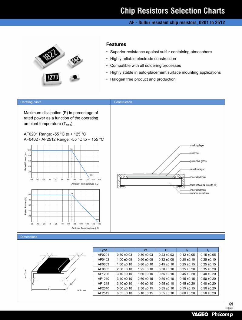
69
Derating curve Construction
Maximum dissipation (P) in percentage of rated power as a function of the operating ambient temperature (Tamb).
AF0201 Range: -55 °C to + 125 °CAF0402 - AF2512 Range: -55 °C to + 155 °C
100
80
60
40
20
-55 -40 -20 0 20 40 60 80
70
100 120 140 160
Ambient Temperature ( C)
Rat
ed P
ower
(%)
125
Dimensions
W
unit: mm
I2
I2
I1
I1
L
H
Type L W H l1 l2AF0201 0.60 ±0.03 0.30 ±0.03 0.23 ±0.03 0.12 ±0.05 0.15 ±0.05AF0402 1.00 ±0.05 0.50 ±0.05 0.32 ±0.05 0.20 ±0.10 0.25 ±0.10 AF0603 1.60 ±0.10 0.80 ±0.10 0.45 ±0.10 0.25 ±0.15 0.25 ±0.15 AF0805 2.00 ±0.10 1.25 ±0.10 0.50 ±0.10 0.35 ±0.20 0.35 ±0.20 AF1206 3.10 ±0.10 1.60 ±0.10 0.55 ±0.10 0.45 ±0.20 0.40 ±0.20 AF1210 3.10 ±0.10 2.60 ±0.15 0.50 ±0.10 0.45 ±0.15 0.50 ±0.20AF1218 3.10 ±0.10 4.60 ±0.10 0.55 ±0.10 0.45 ±0.20 0.40 ±0.20AF2010 5.00 ±0.10 2.50 ±0.15 0.55 ±0.10 0.55 ±0.15 0.50 ±0.20AF2512 6.35 ±0.10 3.10 ±0.15 0.55 ±0.10 0.60 ±0.20 0.50 ±0.20
overcoat
protective glass
resistive layer
inner electrode
termination (Ni / matte tin)
ceramic substrateinner electrode
marking layer
Features• Superior resistance against sulfur containing atmosphere
• Highly reliable electrode construction
• Compatible with all soldering processes
• Highly stable in auto-placement surface mounting applications
• Halogen free product and production
Chip Resistors Selection ChartsAF - Sulfur resistant chip resistors, 0201 to 2512
100
80
60
40
20
-55 -40 -20 0 20 40 60 80
70
100 120 140 160
Ambient Temperature ( C)
Rat
ed P
ower
(%)
155
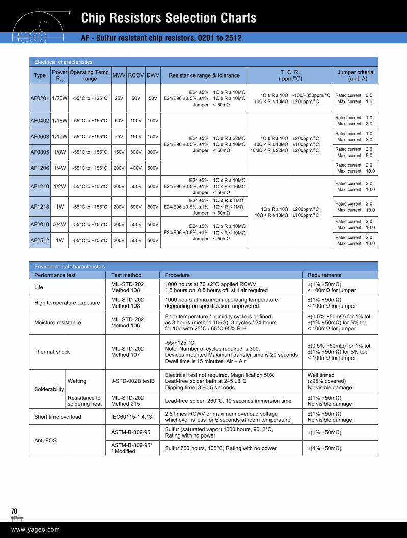
70
Electrical characteristics
Type Power P70
Operating Temp. range MWV RCOV DWV Resistance range & tolerance T. C. R.
( ppm/°C) Jumper criteria
(unit: A)
AF0201 1/20W -55°C to +125°C 25V 50V 50VE24 ±5%
E24/E96 ±0.5%, ±1%Jumper
1Ω ≤ R ≤ 10MΩ1Ω ≤ R ≤ 10MΩ< 50mΩ
1Ω ≤ R ≤ 10Ω 10Ω < R ≤ 10MΩ
-100/+350ppm/°C ±200ppm/°C
Rated current Max. current
0.51.0
AF0402 1/16W -55°C to +155°C 50V 100V 100V
E24 ±5%E24/E96 ±0.5%, ±1%
Jumper
1Ω ≤ R ≤ 22MΩ 1Ω ≤ R ≤ 10MΩ < 50mΩ
1Ω ≤ R ≤ 10Ω 10Ω < R ≤ 10MΩ
10MΩ < R ≤ 22MΩ
±200ppm/°C ±100ppm/°C ±200ppm/°C
Rated current Max. current
1.02.0
AF0603 1/10W -55°C to +155°C 75V 150V 150V Rated current Max. current
1.02.0
AF0805 1/8W -55°C to +155°C 150V 300V 300V Rated current Max. current
2.05.0
AF1206 1/4W -55°C to +155°C 200V 400V 500V Rated current Max. current
2.010.0
AF1210 1/2W -55°C to +155°C 200V 500V 500VE24 ±5%
E24/E96 ±0.5%, ±1% Jumper
1Ω ≤ R ≤ 10MΩ 1Ω ≤ R ≤ 10MΩ < 50mΩ
1Ω ≤ R ≤ 10Ω10Ω < R ≤ 10MΩ
±200ppm/°C ±100ppm/°C
Rated current Max. current
2.010.0
AF1218 1W -55°C to +155°C 200V 500V 500VE24 ±5%
E24/E96 ±0.5%, ±1% Jumper
1Ω ≤ R ≤ 1MΩ 1Ω ≤ R ≤ 1MΩ < 50mΩ
Rated current Max. current
2.010.0
AF2010 3/4W -55°C to +155°C 200V 500V 500V E24 ±5%E24/E96 ±0.5%, ±1%
Jumper
1Ω ≤ R ≤ 10MΩ 1Ω ≤ R ≤ 10MΩ < 50mΩ
Rated current Max. current
2.010.0
AF2512 1W -55°C to +155°C 200V 500V 500V Rated current Max. current
2.010.0
Environmental characteristics Performance test Test method Procedure Requirements
Life MIL-STD-202 Method 108
1000 hours at 70 ±2°C applied RCWV 1.5 hours on, 0.5 hours off, still air required
±(1% +50mΩ)< 100mΩ for jumper
High temperature exposure MIL-STD-202 Method 108
1000 hours at maximum operating temperature depending on specification, unpowered
±(1% +50mΩ)< 100mΩ for jumper
Moisture resistance MIL-STD-202 Method 106
Each temperature / humidity cycle is defined as 8 hours (method 106G), 3 cycles / 24 hours for 10d with 25°C / 65°C 95% R.H
±(0.5% +50mΩ) for 1% tol.±(1% +50mΩ) for 5% tol.< 100mΩ for jumper
Thermal shock MIL-STD-202 Method 107
-55/+125 °CNote: Number of cycles required is 300. Devices mounted Maximum transfer time is 20 seconds. Dwell time is 15 minutes. Air – Air
±(0.5% +50mΩ) for 1% tol.±(1% +50mΩ) for 5% tol.< 100mΩ for jumper
Solderability Wetting J-STD-002B testB
Electrical test not required. Magnification 50X Lead-free solder bath at 245 ±3°C Dipping time: 3 ±0.5 seconds
Well tinned (≥95% covered) No visible damage
Resistance to soldering heat
MIL-STD-202 Method 215 Lead-free solder, 260°C, 10 seconds immersion time ±(1% +50mΩ)
No visible damage
Short time overload IEC60115-1 4.13 2.5 times RCWV or maximum overload voltage whichever is less for 5 seconds at room temperature
±(1% +50mΩ)No visible damage
Anti-FOSASTM-B-809-95 Sulfur (saturated vapor) 1000 hours, 90±2°C,
Rating with no power ±(1% +50mΩ)
ASTM-B-809-95** Modified Sulfur 750 hours, 105°C, Rating with no power ±(4% +50mΩ)
Chip Resistors Selection ChartsAF - Sulfur resistant chip resistors, 0201 to 2512
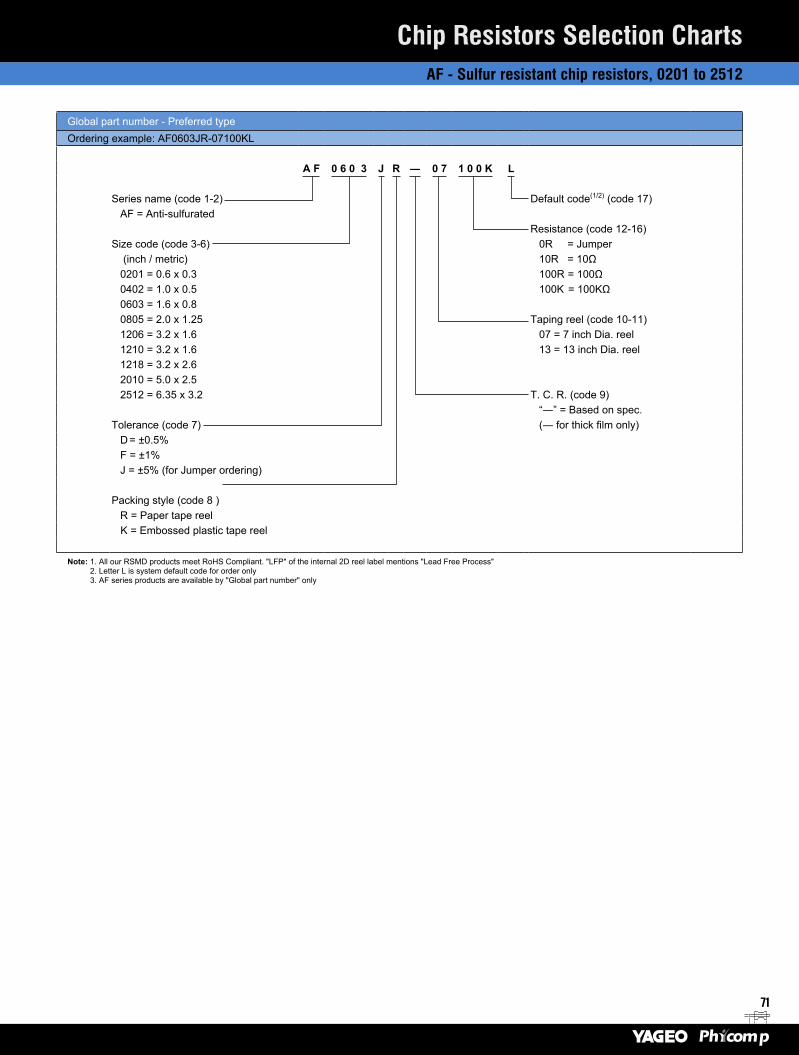
71
Chip Resistors Selection ChartsAF - Sulfur resistant chip resistors, 0201 to 2512
Global part number - Preferred typeOrdering example: AF0603JR-07100KL
A F 0 6 0 3 J R ― 0 7 1 0 0 K L
Series name (code 1-2) Default code(1/2) (code 17)AF = Anti-sulfurated
Resistance (code 12-16)Size code (code 3-6) 0R = Jumper
(inch / metric) 10R = 10Ω0201 = 0.6 x 0.3 100R = 100Ω0402 = 1.0 x 0.5 100K = 100KΩ0603 = 1.6 x 0.80805 = 2.0 x 1.25 Taping reel (code 10-11)1206 = 3.2 x 1.6 07 = 7 inch Dia. reel1210 = 3.2 x 1.6 13 = 13 inch Dia. reel1218 = 3.2 x 2.62010 = 5.0 x 2.52512 = 6.35 x 3.2 T. C. R. (code 9)
“―” = Based on spec.Tolerance (code 7) (― for thick film only)
D = ±0.5%F = ±1%J = ±5% (for Jumper ordering)
Packing style (code 8 )R = Paper tape reel
K = Embossed plastic tape reel
Note: 1. All our RSMD products meet RoHS Compliant. "LFP" of the internal 2D reel label mentions "Lead Free Process" 2. Letter L is system default code for order only 3. AF series products are available by "Global part number" only
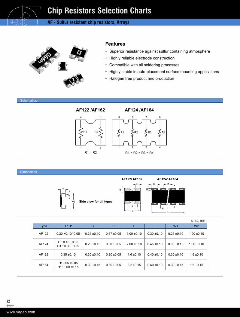
72
Chip Resistors Selection ChartsAF - Sulfur resistant chip resistors, Arrays
Schematics
Dimensions
unit: mmType H / H1 B P L T W1 W2
AF122 0.30 +0.10/-0.05 0.24 ±0.10 0.67 ±0.05 1.00 ±0.10 0.30 ±0.10 0.25 ±0.10 1.00 ±0.10
AF124 H : 0.45 ±0.05H1 : 0.30 ±0.05 0.25 ±0.15 0.50 ±0.05 2.00 ±0.10 0.45 ±0.10 0.30 ±0.15 1.00 ±0.10
AF162 0.35 ±0.10 0.30 ±0.10 0.80 ±0.05 1.6 ±0.10 0.40 ±0.10 0.30 ±0.10 1.6 ±0.10
AF164 H: 0.65 ±0.05 H1: 0.50 ±0.15 0.30 ±0.15 0.80 ±0.05 3.2 ±0.15 0.60 ±0.10 0.30 ±0.15 1.6 ±0.15
Features• Superior resistance against sulfur containing atmosphere
• Highly reliable electrode construction
• Compatible with all soldering processes
• Highly stable in auto-placement surface mounting applications
• Halogen free product and production
AF122 /AF162 AF124 /AF164
Side view for all types
T
W1
W2
H
B
PL
H
L
B
H1
a
a
P
AF122/ AF162 AF124/ AF164
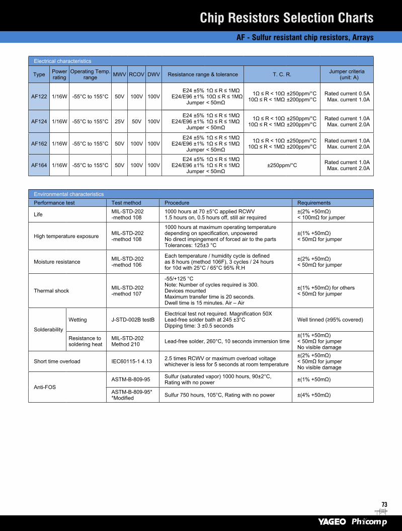
73
Chip Resistors Selection ChartsAF - Sulfur resistant chip resistors, Arrays
Electrical characteristics
Type Power rating
Operating Temp. range MWV RCOV DWV Resistance range & tolerance T. C. R. Jumper criteria
(unit: A)
AF122 1/16W -55°C to 155°C 50V 100V 100V E24 ±5%
E24/E96 ±1% Jumper
1Ω ≤ R ≤ 1MΩ 10Ω ≤ R ≤ 1MΩ < 50mΩ
1Ω ≤ R < 10Ω10Ω ≤ R < 1MΩ
±250ppm/°C ±200ppm/°C
Rated current Max. current
0.5A1.0A
AF124 1/16W -55°C to 155°C 25V 50V 100V E24 ±5%
E24/E96 ±1% Jumper
1Ω ≤ R ≤ 1MΩ 1Ω ≤ R ≤ 1MΩ < 50mΩ
1Ω ≤ R < 10Ω10Ω ≤ R < 1MΩ
±250ppm/°C ±200ppm/°C
Rated current Max. current
1.0A2.0A
AF162 1/16W -55°C to 155°C 50V 100V 100VE24 ±5%
E24/E96 ±1% Jumper
1Ω ≤ R ≤ 1MΩ 1Ω ≤ R ≤ 1MΩ < 50mΩ
1Ω ≤ R < 10Ω10Ω ≤ R < 1MΩ
±250ppm/°C ±200ppm/°C
Rated current Max. current
1.0A2.0A
AF164 1/16W -55°C to 155°C 50V 100V 100VE24 ±5%
E24/E96 ±1%Jumper
1Ω ≤ R ≤ 1MΩ1Ω ≤ R ≤ 1MΩ< 50mΩ
±250ppm/°C Rated current Max. current
1.0A2.0A
Environmental characteristics Performance test Test method Procedure Requirements
Life MIL-STD-202 -method 108
1000 hours at 70 ±5°C applied RCWV 1.5 hours on, 0.5 hours off, still air required
±(2% +50mΩ)< 100mΩ for jumper
High temperature exposure MIL-STD-202 -method 108
1000 hours at maximum operating temperature depending on specification, unpowered No direct impingement of forced air to the parts Tolerances: 125±3 °C
±(1% +50mΩ)< 50mΩ for jumper
Moisture resistance MIL-STD-202 -method 106
Each temperature / humidity cycle is defined as 8 hours (method 106F), 3 cycles / 24 hours for 10d with 25°C / 65°C 95% R.H
±(2% +50mΩ) < 50mΩ for jumper
Thermal shock MIL-STD-202 -method 107
-55/+125 °C Note: Number of cycles required is 300. Devices mounted Maximum transfer time is 20 seconds. Dwell time is 15 minutes. Air – Air
±(1% +50mΩ) for others< 50mΩ for jumper
Solderability
Wetting J-STD-002B testBElectrical test not required. Magnification 50X Lead-free solder bath at 245 ±3°C Dipping time: 3 ±0.5 seconds
Well tinned (≥95% covered)
Resistance to soldering heat
MIL-STD-202 Method 210 Lead-free solder, 260°C, 10 seconds immersion time
±(1% +50mΩ)< 50mΩ for jumperNo visible damage
Short time overload IEC60115-1 4.13 2.5 times RCWV or maximum overload voltage whichever is less for 5 seconds at room temperature
±(2% +50mΩ)< 50mΩ for jumperNo visible damage
Anti-FOSASTM-B-809-95 Sulfur (saturated vapor) 1000 hours, 90±2°C,
Rating with no power ±(1% +50mΩ)
ASTM-B-809-95**Modified Sulfur 750 hours, 105°C, Rating with no power ±(4% +50mΩ)
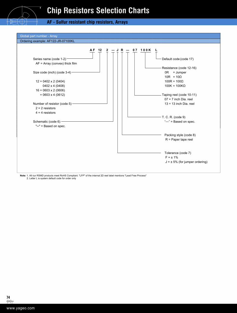
74
Global part number - ArrayOrdering example: AF122-JR-07100KL
A F 12 2 ― J R ― 0 7 1 0 0 K L
Series name (code 1-2) Default code (code 17)AF = Array (convex) thick film
Resistance (code 12-16)Size code (inch) (code 3-4) 0R = Jumper
10R = 10Ω12 = 0402 x 2 (0404) 100R = 100Ω 0402 x 4 (0408) 100K = 100KΩ16 = 0603 x 2 (0606) = 0603 x 4 (0612) Taping reel (code 10-11)
07 = 7 inch Dia. reelNumber of resistor (code 5) 13 = 13 inch Dia. reel
2 = 2 resistors4 = 4 resistors
T. C. R. (code 9)Schematic (code 6) “―” = Based on spec.
"" = Based on spec.
Packing style (code 8) R = Paper tape reel
Tolerance (code 7) F = ± 1% J = ± 5% (for jumper ordering)
Note: 1. All our RSMD products meet RoHS Compliant. "LFP" of the internal 2D reel label mentions "Lead Free Process" 2. Letter L is system default code for order only
Chip Resistors Selection ChartsAF - Sulfur resistant chip resistors, Arrays
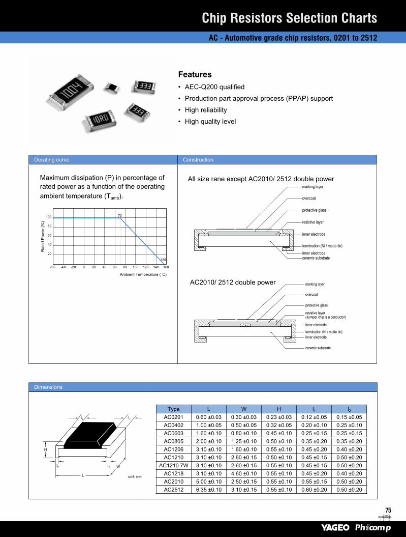
75
Derating curve Construction
Maximum dissipation (P) in percentage of rated power as a function of the operating ambient temperature (Tamb).
100
80
60
40
20
-55 -40 -20 0 20 40 60 80
70
100 120 140 160
Ambient Temperature ( C)
Rat
ed P
ower
(%)
155
Dimensions
W
unit: mm
I2
I2
I1
I1
L
H
Type L W H l1 l2AC0201 0.60 ±0.03 0.30 ±0.03 0.23 ±0.03 0.12 ±0.05 0.15 ±0.05AC0402 1.00 ±0.05 0.50 ±0.05 0.32 ±0.05 0.20 ±0.10 0.25 ±0.10 AC0603 1.60 ±0.10 0.80 ±0.10 0.45 ±0.10 0.25 ±0.15 0.25 ±0.15 AC0805 2.00 ±0.10 1.25 ±0.10 0.50 ±0.10 0.35 ±0.20 0.35 ±0.20 AC1206 3.10 ±0.10 1.60 ±0.10 0.55 ±0.10 0.45 ±0.20 0.40 ±0.20 AC1210 3.10 ±0.10 2.60 ±0.15 0.50 ±0.10 0.45 ±0.15 0.50 ±0.20
AC1210 7W 3.10 ±0.10 2.60 ±0.15 0.55 ±0.10 0.45 ±0.15 0.50 ±0.20AC1218 3.10 ±0.10 4.60 ±0.10 0.55 ±0.10 0.45 ±0.20 0.40 ±0.20AC2010 5.00 ±0.10 2.50 ±0.15 0.55 ±0.10 0.55 ±0.15 0.50 ±0.20AC2512 6.35 ±0.10 3.10 ±0.15 0.55 ±0.10 0.60 ±0.20 0.50 ±0.20
Chip Resistors Selection ChartsAC - Automotive grade chip resistors, 0201 to 2512
Features• AEC-Q200 qualified
• Production part approval process (PPAP) support
• High reliability
• High quality level
overcoat
protective glass
resistive layer
inner electrode
termination (Ni / matte tin)
ceramic substrateinner electrode
marking layer
marking layer
overcoat
protective glass
resistive layer(Jumper chip is a conductor)
inner electrode
inner electrodetermination (Ni / matte tin)
ceramic substrate
All size rane except AC2010/ 2512 double power
AC2010/ 2512 double power
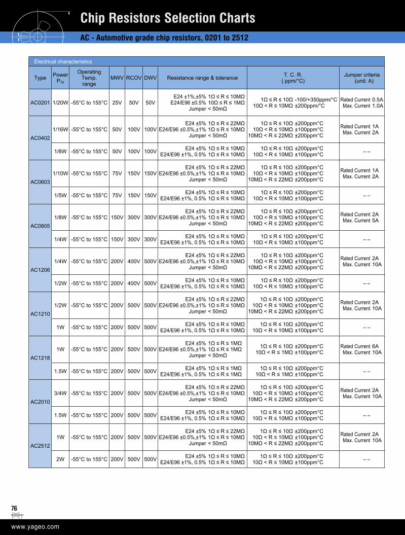
76
Chip Resistors Selection ChartsAC - Automotive grade chip resistors, 0201 to 2512
Electrical characteristics
Type Power P70
Operating Temp. range
MWV RCOV DWV Resistance range & tolerance T. C. R. ( ppm/°C)
Jumper criteria (unit: A)
AC0201 1/20W -55°C to 155°C 25V 50V 50VE24 ±1%,±5%
E24/E96 ±0.5%Jumper
1Ω ≤ R ≤ 10MΩ10Ω ≤ R ≤ 1MΩ< 50mΩ
1Ω ≤ R ≤ 10Ω10Ω < R ≤ 10MΩ
-100/+350ppm/°C±200ppm/°C
Rated CurrentMax. Current
0.5A1.0A
AC04021/16W -55°C to 155°C 50V 100V 100V
E24 ±5% E24/E96 ±0.5%,±1%
Jumper
1Ω ≤ R ≤ 22MΩ 1Ω ≤ R ≤ 10MΩ < 50mΩ
1Ω ≤ R ≤ 10Ω10Ω < R ≤ 10MΩ
10MΩ < R ≤ 22MΩ
±200ppm°C±100ppm°C±200ppm°C
Rated CurrentMax. Current
1A2A
1/8W -55°C to 155°C 50V 100V 100V E24 ±5%E24/E96 ±1%, 0.5%
1Ω ≤ R ≤ 10MΩ1Ω ≤ R ≤ 10MΩ
1Ω ≤ R ≤ 10Ω10Ω < R ≤ 10MΩ
±200ppm°C±100ppm°C -- --
AC06031/10W -55°C to 155°C 75V 150V 150V
E24 ±5% E24/E96 ±0.5%,±1%
Jumper
1Ω ≤ R ≤ 22MΩ 1Ω ≤ R ≤ 10MΩ < 50mΩ
1Ω ≤ R ≤ 10Ω10Ω < R ≤ 10MΩ
10MΩ < R ≤ 22MΩ
±200ppm°C±100ppm°C±200ppm°C
Rated CurrentMax. Current
1A2A
1/5W -55°C to 155°C 75V 150V 150V E24 ±5%E24/E96 ±1%, 0.5%
1Ω ≤ R ≤ 10MΩ1Ω ≤ R ≤ 10MΩ
1Ω ≤ R ≤ 10Ω10Ω < R ≤ 10MΩ
±200ppm°C±100ppm°C -- --
AC08051/8W -55°C to 155°C 150V 300V 300V
E24 ±5% E24/E96 ±0.5%,±1%
Jumper
1Ω ≤ R ≤ 22MΩ 1Ω ≤ R ≤ 10MΩ < 50mΩ
1Ω ≤ R ≤ 10Ω10Ω < R ≤ 10MΩ
10MΩ < R ≤ 22MΩ
±200ppm°C±100ppm°C±200ppm°C
Rated CurrentMax. Current
2A5A
1/4W -55°C to 155°C 150V 300V 300V E24 ±5%E24/E96 ±1%, 0.5%
1Ω ≤ R ≤ 10MΩ1Ω ≤ R ≤ 10MΩ
1Ω ≤ R ≤ 10Ω10Ω < R ≤ 10MΩ
±200ppm°C±100ppm°C -- --
AC12061/4W -55°C to 155°C 200V 400V 500V
E24 ±5% E24/E96 ±0.5%,±1%
Jumper
1Ω ≤ R ≤ 22MΩ 1Ω ≤ R ≤ 10MΩ < 50mΩ
1Ω ≤ R ≤ 10Ω10Ω < R ≤ 10MΩ
10MΩ < R ≤ 22MΩ
±200ppm°C±100ppm°C±200ppm°C
Rated CurrentMax. Current
2A10A
1/2W -55°C to 155°C 200V 400V 500V E24 ±5%E24/E96 ±1%, 0.5%
1Ω ≤ R ≤ 10MΩ1Ω ≤ R ≤ 10MΩ
1Ω ≤ R ≤ 10Ω10Ω < R ≤ 10MΩ
±200ppm°C±100ppm°C -- --
AC12101/2W -55°C to 155°C 200V 500V 500V
E24 ±5%E24/E96 ±0.5%,±1%
Jumper
1Ω ≤ R ≤ 22MΩ1Ω ≤ R ≤ 10MΩ< 50mΩ
1Ω ≤ R ≤ 10Ω10Ω < R ≤ 10MΩ
10MΩ < R ≤ 22MΩ
±200ppm°C±100ppm°C±200ppm°C
Rated CurrentMax. Current
2A10A
1W -55°C to 155°C 200V 500V 500V E24 ±5%E24/E96 ±1%, 0.5%
1Ω ≤ R ≤ 10MΩ1Ω ≤ R ≤ 10MΩ
1Ω ≤ R ≤ 10Ω10Ω < R ≤ 10MΩ
±200ppm°C±100ppm°C -- --
AC12181W -55°C to 155°C 200V 500V 500V
E24 ±5%E24/E96 ±0.5%,±1%
Jumper
1Ω ≤ R ≤ 1MΩ1Ω ≤ R ≤ 1MΩ< 50mΩ
1Ω ≤ R ≤ 10Ω10Ω < R ≤ 1MΩ
±200ppm°C±100ppm°C
Rated CurrentMax. Current
6A10A
1.5W -55°C to 155°C 200V 500V 500V E24 ±5%E24/E96 ±1%, 0.5%
1Ω ≤ R ≤ 1MΩ1Ω ≤ R ≤ 1MΩ
1Ω ≤ R ≤ 10Ω10Ω < R ≤ 1MΩ
±200ppm°C±100ppm°C -- --
AC20103/4W -55°C to 155°C 200V 500V 500V
E24 ±5%E24/E96 ±0.5%,±1%
Jumper
1Ω ≤ R ≤ 22MΩ1Ω ≤ R ≤ 10MΩ< 50mΩ
1Ω ≤ R ≤ 10Ω10Ω < R ≤ 10MΩ
10MΩ < R ≤ 22MΩ
±200ppm°C±100ppm°C±200ppm°C
Rated CurrentMax. Current
2A10A
1.5W -55°C to 155°C 200V 500V 500V E24 ±5%E24/E96 ±1%, 0.5%
1Ω ≤ R ≤ 10MΩ1Ω ≤ R ≤ 10MΩ
1Ω ≤ R ≤ 10Ω10Ω < R ≤ 10MΩ
±200ppm°C±100ppm°C -- --
AC25121W -55°C to 155°C 200V 500V 500V
E24 ±5%E24/E96 ±0.5%,±1%
Jumper
1Ω ≤ R ≤ 22MΩ1Ω ≤ R ≤ 10MΩ< 50mΩ
1Ω ≤ R ≤ 10Ω10Ω < R ≤ 10MΩ
10MΩ < R ≤ 22MΩ
±200ppm°C±100ppm°C±200ppm°C
Rated CurrentMax. Current
2A10A
2W -55°C to 155°C 200V 500V 500V E24 ±5%E24/E96 ±1%, 0.5%
1Ω ≤ R ≤ 10MΩ1Ω ≤ R ≤ 10MΩ
1Ω ≤ R ≤ 10Ω10Ω < R ≤ 10MΩ
±200ppm°C±100ppm°C -- --
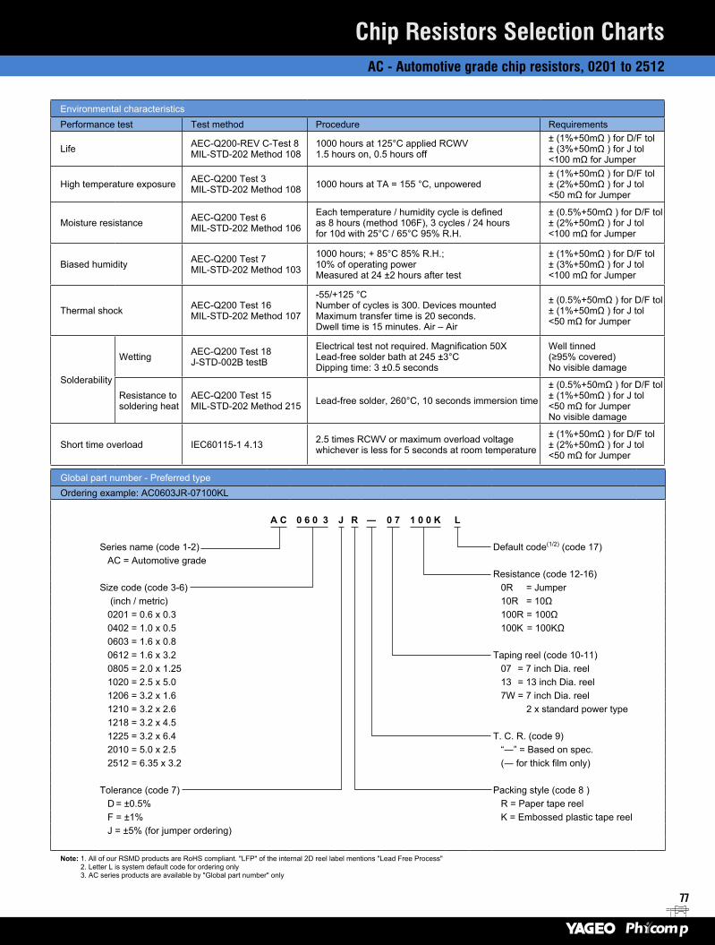
77
Chip Resistors Selection ChartsAC - Automotive grade chip resistors, 0201 to 2512
Environmental characteristics Performance test Test method Procedure Requirements
Life AEC-Q200-REV C-Test 8 MIL-STD-202 Method 108
1000 hours at 125°C applied RCWV 1.5 hours on, 0.5 hours off
± (1%+50mΩ ) for D/F tol ± (3%+50mΩ ) for J tol <100 mΩ for Jumper
High temperature exposure AEC-Q200 Test 3 MIL-STD-202 Method 108 1000 hours at TA = 155 °C, unpowered
± (1%+50mΩ ) for D/F tol ± (2%+50mΩ ) for J tol <50 mΩ for Jumper
Moisture resistance AEC-Q200 Test 6 MIL-STD-202 Method 106
Each temperature / humidity cycle is defined as 8 hours (method 106F), 3 cycles / 24 hours for 10d with 25°C / 65°C 95% R.H.
± (0.5%+50mΩ ) for D/F tol ± (2%+50mΩ ) for J tol <100 mΩ for Jumper
Biased humidity AEC-Q200 Test 7 MIL-STD-202 Method 103
1000 hours; + 85°C 85% R.H.; 10% of operating power Measured at 24 ±2 hours after test
± (1%+50mΩ ) for D/F tol ± (3%+50mΩ ) for J tol <100 mΩ for Jumper
Thermal shock AEC-Q200 Test 16 MIL-STD-202 Method 107
-55/+125 °C Number of cycles is 300. Devices mounted Maximum transfer time is 20 seconds. Dwell time is 15 minutes. Air – Air
± (0.5%+50mΩ ) for D/F tol ± (1%+50mΩ ) for J tol <50 mΩ for Jumper
Solderability
Wetting AEC-Q200 Test 18 J-STD-002B testB
Electrical test not required. Magnification 50X Lead-free solder bath at 245 ±3°C Dipping time: 3 ±0.5 seconds
Well tinned (≥95% covered) No visible damage
Resistance to soldering heat
AEC-Q200 Test 15 MIL-STD-202 Method 215 Lead-free solder, 260°C, 10 seconds immersion time
± (0.5%+50mΩ ) for D/F tol ± (1%+50mΩ ) for J tol <50 mΩ for Jumper No visible damage
Short time overload IEC60115-1 4.13 2.5 times RCWV or maximum overload voltage whichever is less for 5 seconds at room temperature
± (1%+50mΩ ) for D/F tol ± (2%+50mΩ ) for J tol <50 mΩ for Jumper
Global part number - Preferred typeOrdering example: AC0603JR-07100KL
A C 0 6 0 3 J R ― 0 7 1 0 0 K L
Series name (code 1-2) Default code(1/2) (code 17)AC = Automotive grade
Resistance (code 12-16)Size code (code 3-6) 0R = Jumper
(inch / metric) 10R = 10Ω0201 = 0.6 x 0.3 100R = 100Ω0402 = 1.0 x 0.5 100K = 100KΩ0603 = 1.6 x 0.80612 = 1.6 x 3.2 Taping reel (code 10-11)0805 = 2.0 x 1.25 07 = 7 inch Dia. reel1020 = 2.5 x 5.0 13 = 13 inch Dia. reel1206 = 3.2 x 1.6 7W = 7 inch Dia. reel1210 = 3.2 x 2.6 2 x standard power type1218 = 3.2 x 4.51225 = 3.2 x 6.4 T. C. R. (code 9)2010 = 5.0 x 2.5 “―” = Based on spec.2512 = 6.35 x 3.2 (― for thick film only)
Tolerance (code 7) Packing style (code 8 )D = ±0.5% R = Paper tape reelF = ±1% K = Embossed plastic tape reelJ = ±5% (for jumper ordering)
Note: 1. All of our RSMD products are RoHS compliant. "LFP" of the internal 2D reel label mentions "Lead Free Process" 2. Letter L is system default code for ordering only 3. AC series products are available by "Global part number" only
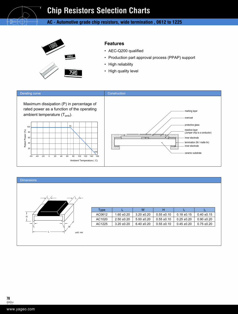
78
Derating curve Construction
Maximum dissipation (P) in percentage of rated power as a function of the operating ambient temperature (Tamb).
100
80
60
40
20
-55 -40 -20 0 20 40 60 80
70
100 120 140 160
Ambient Temperature ( C)
Rat
ed P
ower
(%)
155
Dimensions
W
unit: mm
I2
I2
I1
I1
L
H
Type L W H l1 l2AC0612 1.60 ±0.20 3.20 ±0.20 0.55 ±0.10 0.18 ±0.15 0.40 ±0.15AC1020 2.50 ±0.20 5.00 ±0.20 0.55 ±0.10 0.25 ±0.20 0.90 ±0.20AC1225 3.20 ±0.20 6.40 ±0.20 0.55 ±0.10 0.45 ±0.20 0.75 ±0.20
Chip Resistors Selection ChartsAC - Automotive grade chip resistors, wide termination , 0612 to 1225
Features• AEC-Q200 qualified
• Production part approval process (PPAP) support
• High reliability
• High quality level
marking layer
overcoat
protective glass
resistive layer(Jumper chip is a conductor)
inner electrode
inner electrodetermination (Ni / matte tin)
ceramic substrate
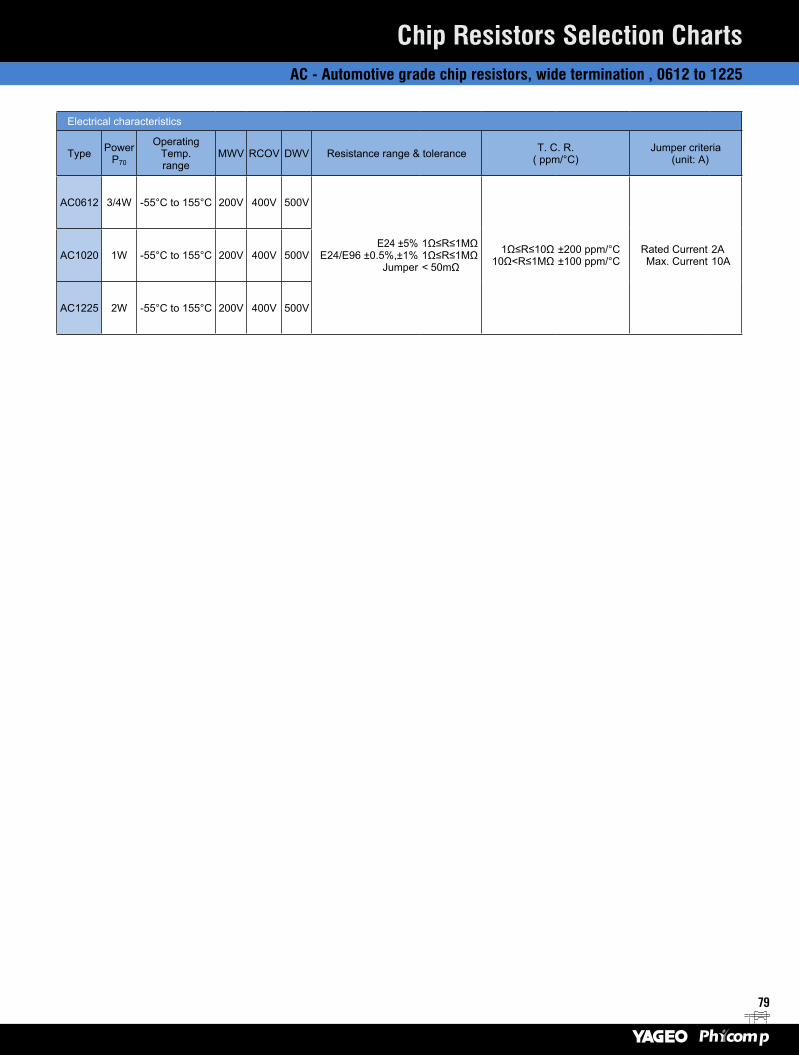
79
Chip Resistors Selection ChartsAC - Automotive grade chip resistors, wide termination , 0612 to 1225
Electrical characteristics
Type Power P70
Operating Temp. range
MWV RCOV DWV Resistance range & tolerance T. C. R. ( ppm/°C)
Jumper criteria (unit: A)
AC0612 3/4W -55°C to 155°C 200V 400V 500V
E24 ±5%E24/E96 ±0.5%,±1%
Jumper
1Ω≤R≤1MΩ1Ω≤R≤1MΩ< 50mΩ
1Ω≤R≤10Ω10Ω<R≤1MΩ
±200 ppm/°C±100 ppm/°C
Rated CurrentMax. Current
2A10AAC1020 1W -55°C to 155°C 200V 400V 500V
AC1225 2W -55°C to 155°C 200V 400V 500V
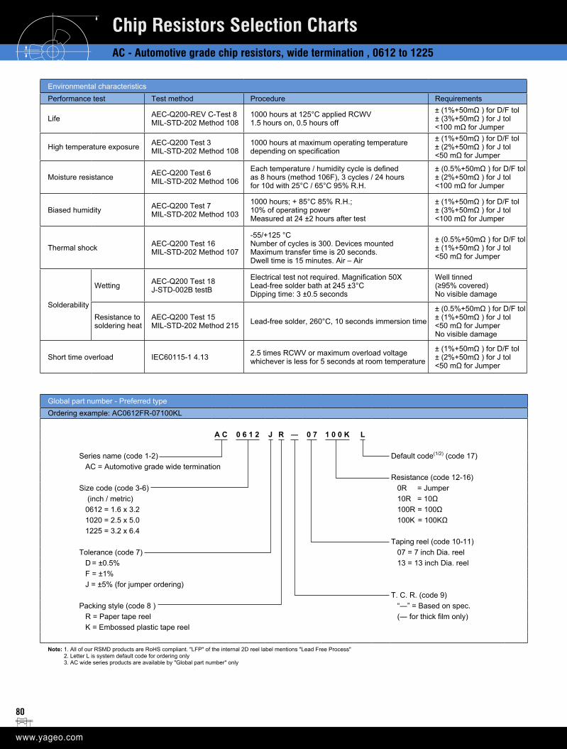
80
Chip Resistors Selection ChartsAC - Automotive grade chip resistors, wide termination , 0612 to 1225
Environmental characteristics Performance test Test method Procedure Requirements
Life AEC-Q200-REV C-Test 8 MIL-STD-202 Method 108
1000 hours at 125°C applied RCWV 1.5 hours on, 0.5 hours off
± (1%+50mΩ ) for D/F tol ± (3%+50mΩ ) for J tol <100 mΩ for Jumper
High temperature exposure AEC-Q200 Test 3 MIL-STD-202 Method 108
1000 hours at maximum operating temperature depending on specification
± (1%+50mΩ ) for D/F tol ± (2%+50mΩ ) for J tol <50 mΩ for Jumper
Moisture resistance AEC-Q200 Test 6 MIL-STD-202 Method 106
Each temperature / humidity cycle is defined as 8 hours (method 106F), 3 cycles / 24 hours for 10d with 25°C / 65°C 95% R.H.
± (0.5%+50mΩ ) for D/F tol ± (2%+50mΩ ) for J tol <100 mΩ for Jumper
Biased humidity AEC-Q200 Test 7 MIL-STD-202 Method 103
1000 hours; + 85°C 85% R.H.; 10% of operating power Measured at 24 ±2 hours after test
± (1%+50mΩ ) for D/F tol ± (3%+50mΩ ) for J tol <100 mΩ for Jumper
Thermal shock AEC-Q200 Test 16 MIL-STD-202 Method 107
-55/+125 °C Number of cycles is 300. Devices mounted Maximum transfer time is 20 seconds. Dwell time is 15 minutes. Air – Air
± (0.5%+50mΩ ) for D/F tol ± (1%+50mΩ ) for J tol <50 mΩ for Jumper
Solderability
Wetting AEC-Q200 Test 18 J-STD-002B testB
Electrical test not required. Magnification 50X Lead-free solder bath at 245 ±3°C Dipping time: 3 ±0.5 seconds
Well tinned (≥95% covered) No visible damage
Resistance to soldering heat
AEC-Q200 Test 15 MIL-STD-202 Method 215 Lead-free solder, 260°C, 10 seconds immersion time
± (0.5%+50mΩ ) for D/F tol ± (1%+50mΩ ) for J tol <50 mΩ for Jumper No visible damage
Short time overload IEC60115-1 4.13 2.5 times RCWV or maximum overload voltage whichever is less for 5 seconds at room temperature
± (1%+50mΩ ) for D/F tol ± (2%+50mΩ ) for J tol <50 mΩ for Jumper
Global part number - Preferred typeOrdering example: AC0612FR-07100KL
A C 0 6 1 2 J R ― 0 7 1 0 0 K L
Series name (code 1-2) Default code(1/2) (code 17)AC = Automotive grade wide termination
Resistance (code 12-16)Size code (code 3-6) 0R = Jumper
(inch / metric) 10R = 10Ω0612 = 1.6 x 3.2 100R = 100Ω1020 = 2.5 x 5.0 100K = 100KΩ1225 = 3.2 x 6.4
Taping reel (code 10-11)Tolerance (code 7) 07 = 7 inch Dia. reel
D = ±0.5% 13 = 13 inch Dia. reelF = ±1%J = ±5% (for jumper ordering)
T. C. R. (code 9)Packing style (code 8 ) “―” = Based on spec.
R = Paper tape reel (― for thick film only)K = Embossed plastic tape reel
Note: 1. All of our RSMD products are RoHS compliant. "LFP" of the internal 2D reel label mentions "Lead Free Process" 2. Letter L is system default code for ordering only 3. AC wide series products are available by "Global part number" only
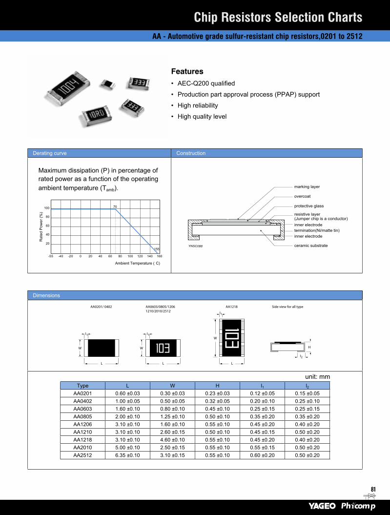
81
Derating curve Construction
Maximum dissipation (P) in percentage of rated power as a function of the operating ambient temperature (Tamb).
100
80
60
40
20
-55 -40 -20 0 20 40 60 80
70
100 120 140 160
Ambient Temperature ( C)
Rat
ed P
ower
(%)
155
Dimensions
I1
I2
I1
L L
HW
I1
L
W
W
AA0201/ 0402 AA0603/0805/12061210/2010/2512
AA1218 Side view for all type
unit: mmType L W H l1 l2
AA0201 0.60 ±0.03 0.30 ±0.03 0.23 ±0.03 0.12 ±0.05 0.15 ±0.05AA0402 1.00 ±0.05 0.50 ±0.05 0.32 ±0.05 0.20 ±0.10 0.25 ±0.10 AA0603 1.60 ±0.10 0.80 ±0.10 0.45 ±0.10 0.25 ±0.15 0.25 ±0.15 AA0805 2.00 ±0.10 1.25 ±0.10 0.50 ±0.10 0.35 ±0.20 0.35 ±0.20 AA1206 3.10 ±0.10 1.60 ±0.10 0.55 ±0.10 0.45 ±0.20 0.40 ±0.20 AA1210 3.10 ±0.10 2.60 ±0.15 0.50 ±0.10 0.45 ±0.15 0.50 ±0.20AA1218 3.10 ±0.10 4.60 ±0.10 0.55 ±0.10 0.45 ±0.20 0.40 ±0.20AA2010 5.00 ±0.10 2.50 ±0.15 0.55 ±0.10 0.55 ±0.15 0.50 ±0.20AA2512 6.35 ±0.10 3.10 ±0.15 0.55 ±0.10 0.60 ±0.20 0.50 ±0.20
Chip Resistors Selection ChartsAA - Automotive grade sulfur-resistant chip resistors,0201 to 2512
Features• AEC-Q200 qualified
• Production part approval process (PPAP) support
• High reliability
• High quality level
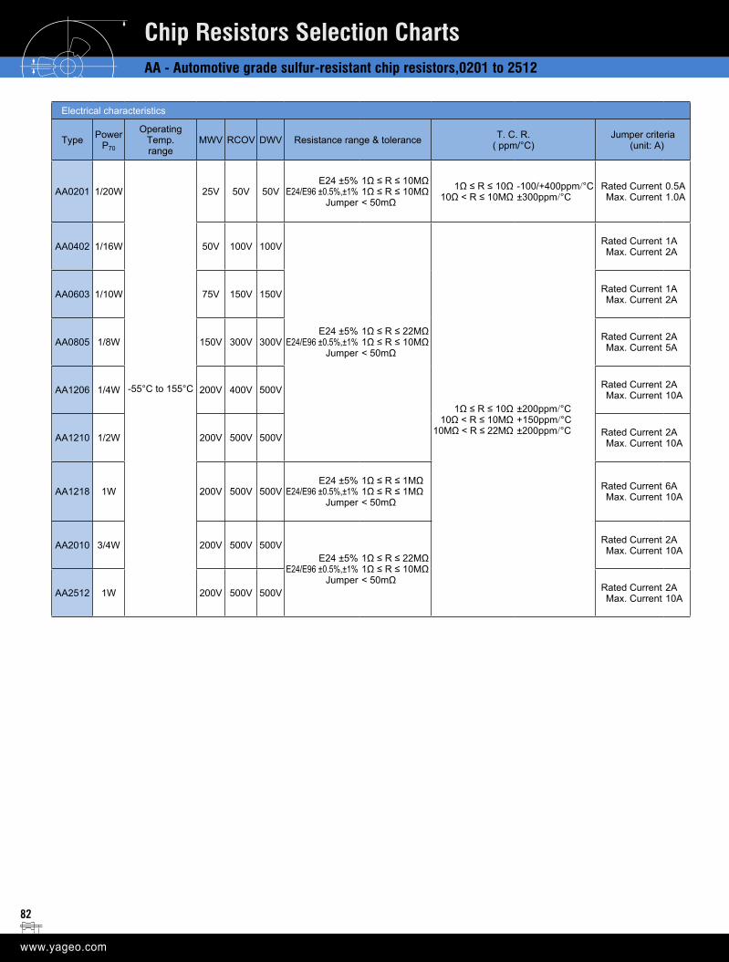
82
Chip Resistors Selection ChartsAA - Automotive grade sulfur-resistant chip resistors,0201 to 2512
Electrical characteristics
Type Power P70
Operating Temp. range
MWV RCOV DWV Resistance range & tolerance T. C. R. ( ppm/°C)
Jumper criteria (unit: A)
AA0201 1/20W
-55°C to 155°C
25V 50V 50VE24 ±5%
E24/E96 ±0.5%,±1%Jumper
1Ω ≤ R ≤ 10MΩ1Ω ≤ R ≤ 10MΩ< 50mΩ
1Ω ≤ R ≤ 10Ω10Ω < R ≤ 10MΩ
-100/+400ppm/°C±300ppm/°C
Rated CurrentMax. Current
0.5A1.0A
AA0402 1/16W 50V 100V 100V
E24 ±5%E24/E96 ±0.5%,±1%
Jumper
1Ω ≤ R ≤ 22MΩ1Ω ≤ R ≤ 10MΩ< 50mΩ
1Ω ≤ R ≤ 10Ω10Ω < R ≤ 10MΩ
10MΩ < R ≤ 22MΩ
±200ppm/°C+150ppm/°C±200ppm/°C
Rated CurrentMax. Current
1A2A
AA0603 1/10W 75V 150V 150V Rated CurrentMax. Current
1A2A
AA0805 1/8W 150V 300V 300V Rated CurrentMax. Current
2A5A
AA1206 1/4W 200V 400V 500V Rated CurrentMax. Current
2A10A
AA1210 1/2W 200V 500V 500V Rated CurrentMax. Current
2A10A
AA1218 1W 200V 500V 500VE24 ±5%
E24/E96 ±0.5%,±1%Jumper
1Ω ≤ R ≤ 1MΩ1Ω ≤ R ≤ 1MΩ< 50mΩ
Rated CurrentMax. Current
6A10A
AA2010 3/4W 200V 500V 500VE24 ±5%
E24/E96 ±0.5%,±1%Jumper
1Ω ≤ R ≤ 22MΩ1Ω ≤ R ≤ 10MΩ< 50mΩ
Rated CurrentMax. Current
2A10A
AA2512 1W 200V 500V 500V Rated CurrentMax. Current
2A10A
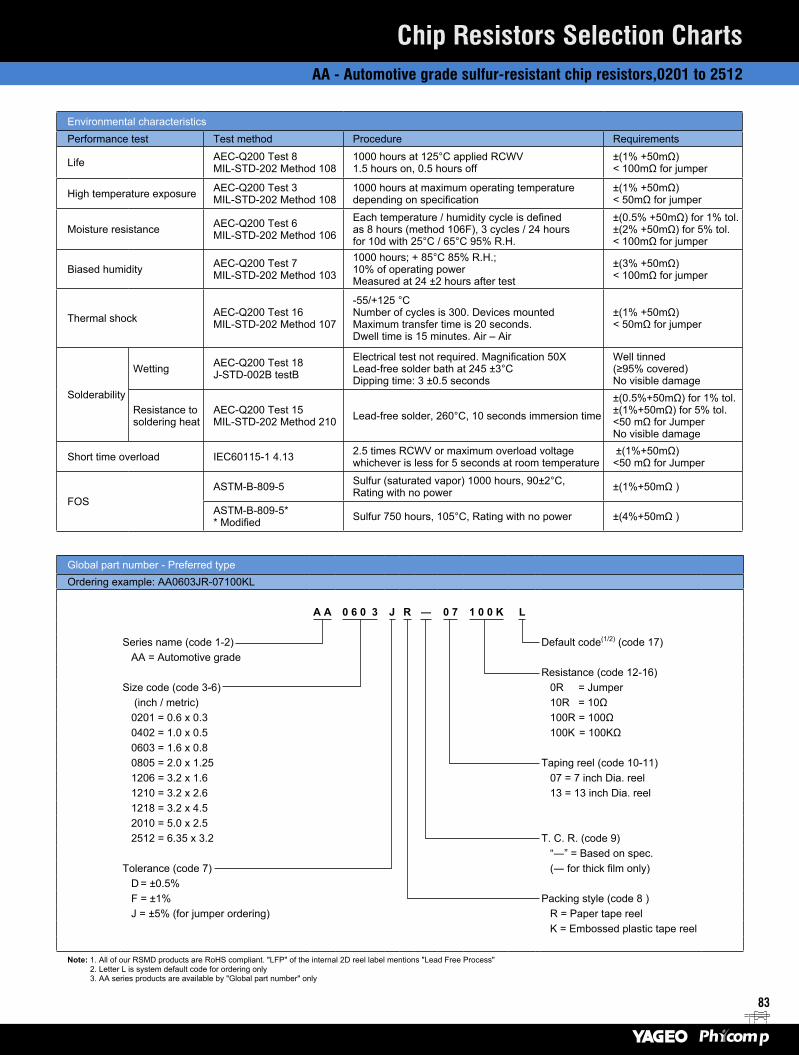
83
Chip Resistors Selection ChartsAA - Automotive grade sulfur-resistant chip resistors,0201 to 2512
Environmental characteristics Performance test Test method Procedure Requirements
Life AEC-Q200 Test 8 MIL-STD-202 Method 108
1000 hours at 125°C applied RCWV 1.5 hours on, 0.5 hours off
±(1% +50mΩ)< 100mΩ for jumper
High temperature exposure AEC-Q200 Test 3 MIL-STD-202 Method 108
1000 hours at maximum operating temperature depending on specification
±(1% +50mΩ)< 50mΩ for jumper
Moisture resistance AEC-Q200 Test 6 MIL-STD-202 Method 106
Each temperature / humidity cycle is defined as 8 hours (method 106F), 3 cycles / 24 hours for 10d with 25°C / 65°C 95% R.H.
±(0.5% +50mΩ) for 1% tol.±(2% +50mΩ) for 5% tol.< 100mΩ for jumper
Biased humidity AEC-Q200 Test 7 MIL-STD-202 Method 103
1000 hours; + 85°C 85% R.H.; 10% of operating power Measured at 24 ±2 hours after test
±(3% +50mΩ)< 100mΩ for jumper
Thermal shock AEC-Q200 Test 16 MIL-STD-202 Method 107
-55/+125 °C Number of cycles is 300. Devices mounted Maximum transfer time is 20 seconds. Dwell time is 15 minutes. Air – Air
±(1% +50mΩ)< 50mΩ for jumper
Solderability
Wetting AEC-Q200 Test 18 J-STD-002B testB
Electrical test not required. Magnification 50X Lead-free solder bath at 245 ±3°C Dipping time: 3 ±0.5 seconds
Well tinned (≥95% covered) No visible damage
Resistance to soldering heat
AEC-Q200 Test 15 MIL-STD-202 Method 210 Lead-free solder, 260°C, 10 seconds immersion time
±(0.5%+50mΩ) for 1% tol. ±(1%+50mΩ) for 5% tol. <50 mΩ for Jumper No visible damage
Short time overload IEC60115-1 4.13 2.5 times RCWV or maximum overload voltage whichever is less for 5 seconds at room temperature
±(1%+50mΩ) <50 mΩ for Jumper
FOSASTM-B-809-5 Sulfur (saturated vapor) 1000 hours, 90±2°C,
Rating with no power ±(1%+50mΩ )
ASTM-B-809-5* * Modified Sulfur 750 hours, 105°C, Rating with no power ±(4%+50mΩ )
Global part number - Preferred typeOrdering example: AA0603JR-07100KL
A A 0 6 0 3 J R ― 0 7 1 0 0 K L
Series name (code 1-2) Default code(1/2) (code 17)AA = Automotive grade
Resistance (code 12-16)Size code (code 3-6) 0R = Jumper
(inch / metric) 10R = 10Ω0201 = 0.6 x 0.3 100R = 100Ω0402 = 1.0 x 0.5 100K = 100KΩ0603 = 1.6 x 0.80805 = 2.0 x 1.25 Taping reel (code 10-11)1206 = 3.2 x 1.6 07 = 7 inch Dia. reel1210 = 3.2 x 2.6 13 = 13 inch Dia. reel1218 = 3.2 x 4.52010 = 5.0 x 2.52512 = 6.35 x 3.2 T. C. R. (code 9)
“―” = Based on spec.Tolerance (code 7) (― for thick film only)
D = ±0.5%F = ±1% Packing style (code 8 )J = ±5% (for jumper ordering) R = Paper tape reel
K = Embossed plastic tape reel
Note: 1. All of our RSMD products are RoHS compliant. "LFP" of the internal 2D reel label mentions "Lead Free Process" 2. Letter L is system default code for ordering only 3. AA series products are available by "Global part number" only
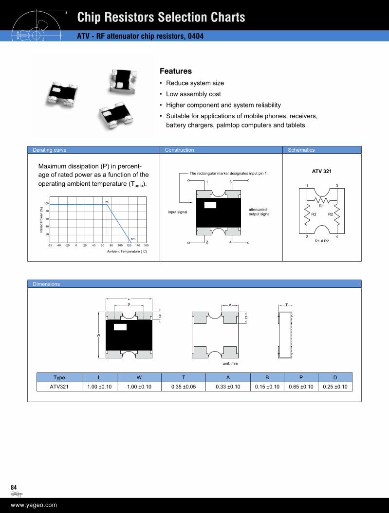
84
Features• Reduce system size
• Low assembly cost
• Higher component and system reliability
• Suitable for applications of mobile phones, receivers, battery chargers, palmtop computers and tablets
Derating curve Construction Schematics
Maximum dissipation (P) in percent-age of rated power as a function of the operating ambient temperature (Tamb).
100
80
60
40
20
-55 -40 -20 0 20 40 60 80
70
100 120 140 160
Ambient Temperature ( C)
Rat
ed P
ower
(%)
125
1 3
2 4
input signal attenuated output signal
The rectangular marker designates input pin 1
1 3
R2R2
R1
2 4
ATV 321
Dimensions
LP
B
W
T
D
A
unit: mm
Type L W T A B P D
ATV321 1.00 ±0.10 1.00 ±0.10 0.35 ±0.05 0.33 ±0.10 0.15 ±0.10 0.65 ±0.10 0.25 ±0.10
Chip Resistors Selection ChartsATV - RF attenuator chip resistors, 0404
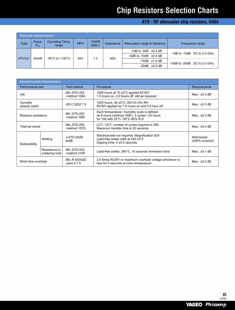
85
Electrical characteristics
Type Power P70
Operating Temp. range MPV VSWR
(Max.) Impedance Attenuation range & tolerance Frequency range
ATV321 40mW -55°C to +125°C 50V 1.3 50Ω
-1dB to -5dB ±0.3 dB-1dB to -10dB DC to 2.5 GHz
-6dB to -10dB ±0.5 dB-15dB ±1.0 dB
-15dB to -20dB DC to 2.0 GHz -20dB ±2.0 dB
Environmental characteristics
Performance test Test method Procedure Requirements
Life MIL-STD-202 -method 108A
1000 hours at 70 ±5°C applied RCWV 1.5 hours on, 0.5 hours off, still air required Max.: ±0.3 dB
Humidity (steady state) JIS C 5202 7.5 1000 hours, 40 ±2°C, 93(+2/-3)% RH
RCWV applied for 1.5 hours on and 0.5 hour off Max.: ±0.3 dB
Moisture resistance MIL-STD-202 -method 106F
Each temperature / humidity cycle is defined as 8 hours (method 106F), 3 cycles / 24 hours for 10d with 25°C / 65°C 95% R.H
Max.: ±0.3 dB
Thermal shock MIL-STD-202 -method 107G
LCT / UCT, number of cycles required is 300 Maximum transfer time is 20 seconds Max.: ±0.3 dB
Solderability Wetting J-STD-002B
testB
Electrical test not required. Magnification 50X Lead-free solder bath at 245 ±3°C Dipping time: 3 ±0.5 seconds
Well tinned (≥95% covered)
Resistance to soldering heat
MIL-STD-202 -method 210F Lead-free solder, 260°C, 10 seconds immersion time Max.: ±0.1 dB
Short time overload MIL-R-55342D-para 4.7.5
2.5 times RCWV or maximum overload voltage whichever is less for 5 seconds at room temperature Max.: ±0.3 dB
Chip Resistors Selection ChartsATV - RF attenuator chip resistors, 0404
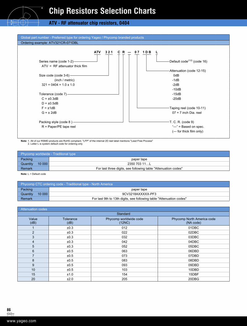
86
Global part number - Preferred type for ordering Yageo / Phycomp branded productsOrdering example: ATV321CR-071DBL
ATV 3 2 1 C R ― 0 7 1 D B L
Series name (code 1-2) Default code(1/2) (code 16)ATV = RF attenuator thick film
Attenuation (code 12-15)Size code (code 3-6) 0dB
(inch / metric) -1dB321 = 0404 = 1.0 x 1.0 -2dB
-10dBTolerance (code 7) -15dB
C = ±0.3dB -20dBD = ±0.5dBF = ±1dB Taping reel (code 10-11)G = ± 2dB 07 = 7 inch Dia. reel
Packing style (code 8 ) T. C. R. (code 9)R = Paper/PE tape reel “―” = Based on spec.
(― for thick film only)
Note: 1. All of our RSMD products are RoHS compliant. "LFP" of the internal 2D reel label mentions "Lead Free Process" 2. Letter L is system default code for ordering only
Phycomp worldwide - Traditional typePacking paper tapeQuantity 10 000 2350 703 11…L Remark For last three digits, see following table "Attenuation codes"Note: L = Default code
Phycomp CTC ordering code - Traditional type - North AmericaPacking paper tapeQuantity 10 000 9CV3218AXXXXX-PF3Remark For last 9th to 13th digits, see following table "Attenuation codes"
Attenuation codesStandard
Value (dB)
Tolerance (dB)
Phycomp worldwide code (12NC)
Phycomp North America code (NA code)
1 ±0.3 012 01DBC2 ±0.3 022 02DBC3 ±0.3 032 03DBC4 ±0.3 042 04DBC5 ±0.3 052 05DBC6 ±0.5 063 06DBD7 ±0.5 073 07DBD8 ±0.5 083 08DBD9 ±0.5 093 09DBD10 ±0.5 103 10DBD15 ±1.0 154 15DBF20 ±2.0 205 20DBG
Chip Resistors Selection ChartsATV - RF attenuator chip resistors, 0404
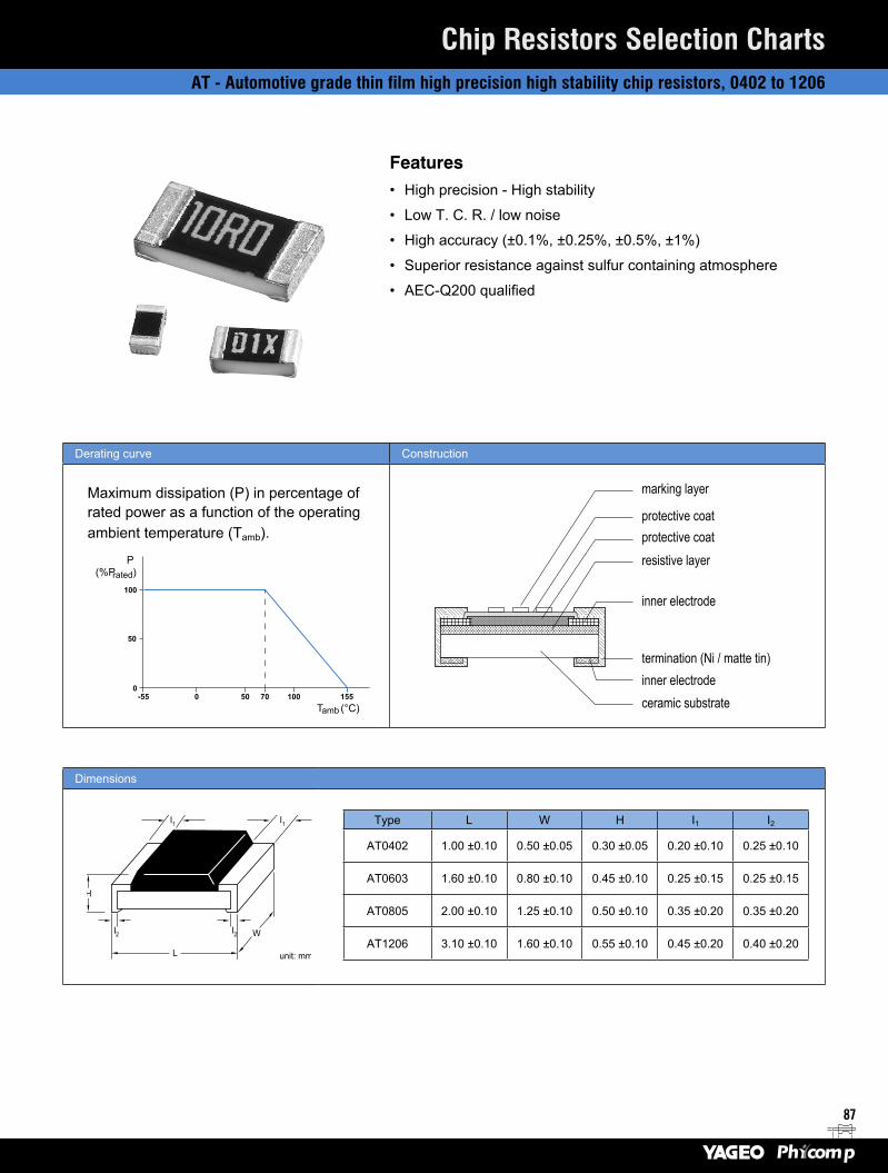
87
Derating curve Construction
Maximum dissipation (P) in percentage of rated power as a function of the operating ambient temperature (Tamb).
-55 00
50
50
70 100
100
155T (°C)amb
P(%P )rated
marking layer
protective coatprotective coatresistive layer
inner electrode
inner electrodetermination (Ni / matte tin)
ceramic substrate
Dimensions
W
unit: mm
I2
I2
I1
I1
L
H
Type L W H I1 I2
AT0402 1.00 ±0.10 0.50 ±0.05 0.30 ±0.05 0.20 ±0.10 0.25 ±0.10
AT0603 1.60 ±0.10 0.80 ±0.10 0.45 ±0.10 0.25 ±0.15 0.25 ±0.15
AT0805 2.00 ±0.10 1.25 ±0.10 0.50 ±0.10 0.35 ±0.20 0.35 ±0.20
AT1206 3.10 ±0.10 1.60 ±0.10 0.55 ±0.10 0.45 ±0.20 0.40 ±0.20
Features• High precision - High stability
• Low T. C. R. / low noise
• High accuracy (±0.1%, ±0.25%, ±0.5%, ±1%)
• Superior resistance against sulfur containing atmosphere
• AEC-Q200 qualified
Chip Resistors Selection ChartsAT - Automotive grade thin film high precision high stability chip resistors, 0402 to 1206
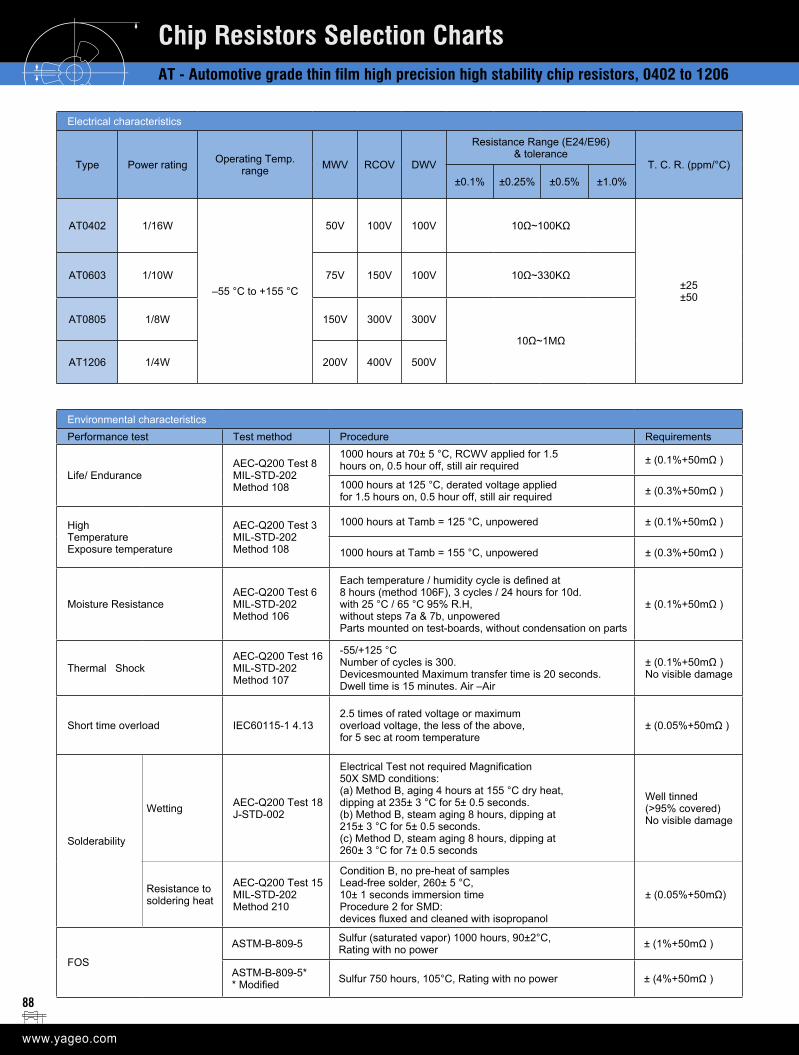
88
Chip Resistors Selection ChartsAT - Automotive grade thin film high precision high stability chip resistors, 0402 to 1206
Electrical characteristics
Type Power rating Operating Temp. range MWV RCOV DWV
Resistance Range (E24/E96) & tolerance
T. C. R. (ppm/°C)±0.1% ±0.25% ±0.5% ±1.0%
AT0402 1/16W
–55 °C to +155 °C
50V 100V 100V 10Ω~100KΩ
±25±50
AT0603 1/10W 75V 150V 100V 10Ω~330KΩ
AT0805 1/8W 150V 300V 300V
10Ω~1MΩ
AT1206 1/4W 200V 400V 500V
Environmental characteristics Performance test Test method Procedure Requirements
Life/ EnduranceAEC-Q200 Test 8 MIL-STD-202 Method 108
1000 hours at 70± 5 °C, RCWV applied for 1.5 hours on, 0.5 hour off, still air required ± (0.1%+50mΩ )
1000 hours at 125 °C, derated voltage applied for 1.5 hours on, 0.5 hour off, still air required ± (0.3%+50mΩ )
High Temperature Exposure temperature
AEC-Q200 Test 3 MIL-STD-202 Method 108
1000 hours at Tamb = 125 °C, unpowered ± (0.1%+50mΩ )
1000 hours at Tamb = 155 °C, unpowered ± (0.3%+50mΩ )
Moisture ResistanceAEC-Q200 Test 6 MIL-STD-202 Method 106
Each temperature / humidity cycle is defined at 8 hours (method 106F), 3 cycles / 24 hours for 10d. with 25 °C / 65 °C 95% R.H, without steps 7a & 7b, unpowered Parts mounted on test-boards, without condensation on parts
± (0.1%+50mΩ )
Thermal ShockAEC-Q200 Test 16 MIL-STD-202 Method 107
-55/+125 °C Number of cycles is 300. Devicesmounted Maximum transfer time is 20 seconds. Dwell time is 15 minutes. Air –Air
± (0.1%+50mΩ ) No visible damage
Short time overload IEC60115-1 4.132.5 times of rated voltage or maximum overload voltage, the less of the above, for 5 sec at room temperature
± (0.05%+50mΩ )
Solderability
Wetting AEC-Q200 Test 18 J-STD-002
Electrical Test not required Magnification 50X SMD conditions: (a) Method B, aging 4 hours at 155 °C dry heat, dipping at 235± 3 °C for 5± 0.5 seconds. (b) Method B, steam aging 8 hours, dipping at 215± 3 °C for 5± 0.5 seconds. (c) Method D, steam aging 8 hours, dipping at 260± 3 °C for 7± 0.5 seconds
Well tinned (>95% covered) No visible damage
Resistance to soldering heat
AEC-Q200 Test 15 MIL-STD-202 Method 210
Condition B, no pre-heat of samples Lead-free solder, 260± 5 °C, 10± 1 seconds immersion time Procedure 2 for SMD: devices fluxed and cleaned with isopropanol
± (0.05%+50mΩ)
FOS
ASTM-B-809-5 Sulfur (saturated vapor) 1000 hours, 90±2°C, Rating with no power ± (1%+50mΩ )
ASTM-B-809-5* * Modified Sulfur 750 hours, 105°C, Rating with no power ± (4%+50mΩ )
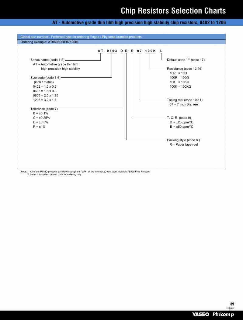
89
Global part number - Preferred type for ordering Yageo / Phycomp branded productsOrdering example: AT0603DRE07100KL
A T 0 6 0 3 D R E 0 7 1 0 0 K L
Series name (code 1-2) Default code (1/2) (code 17) AT = Automotive grade thin film high precision high stability Resistance (code 12-16)
10R = 10ΩSize code (code 3-6) 100R = 100Ω
(inch / metric) 10K = 10KΩ0402 = 1.0 x 0.5 100K = 100KΩ0603 = 1.6 x 0.8 0805 = 2.0 x 1.251206 = 3.2 x 1.6 Taping reel (code 10-11)
07 = 7 inch Dia. reelTolerance (code 7)
B = ±0.1% C = ±0.25% T. C. R. (code 9)D = ±0.5% D = ±25 ppm/°CF = ±1% E = ±50 ppm/°C
Packing style (code 8 )R = Paper tape reel
Note: 1. All of our RSMD products are RoHS compliant. "LFP" of the internal 2D reel label mentions "Lead Free Process" 2. Letter L is system default code for ordering only
Chip Resistors Selection ChartsAT - Automotive grade thin film high precision high stability chip resistors, 0402 to 1206
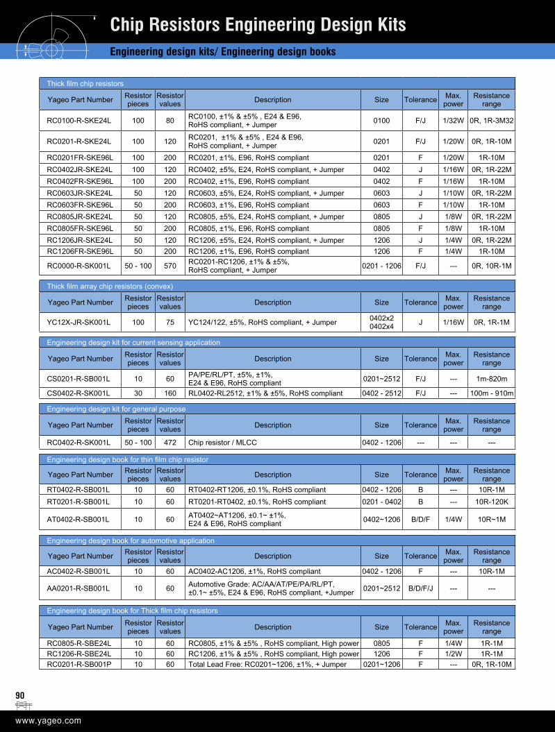
90
Thick film chip resistors
Yageo Part Number Resistor pieces
Resistor values Description Size Tolerance Max.
powerResistance
range
RC0100-R-SKE24L 100 80 RC0100, ±1% & ±5% , E24 & E96, RoHS compliant, + Jumper 0100 F/J 1/32W 0R, 1R-3M32
RC0201-R-SKE24L 100 120 RC0201, ±1% & ±5% , E24 & E96, RoHS compliant, + Jumper 0201 F/J 1/20W 0R, 1R-10M
RC0201FR-SKE96L 100 200 RC0201, ±1%, E96, RoHS compliant 0201 F 1/20W 1R-10MRC0402JR-SKE24L 100 120 RC0402, ±5%, E24, RoHS compliant, + Jumper 0402 J 1/16W 0R, 1R-22MRC0402FR-SKE96L 100 200 RC0402, ±1%, E96, RoHS compliant 0402 F 1/16W 1R-10MRC0603JR-SKE24L 50 120 RC0603, ±5%, E24, RoHS compliant, + Jumper 0603 J 1/10W 0R, 1R-22MRC0603FR-SKE96L 50 200 RC0603, ±1%, E96, RoHS compliant 0603 F 1/10W 1R-10MRC0805JR-SKE24L 50 120 RC0805, ±5%, E24, RoHS compliant, + Jumper 0805 J 1/8W 0R, 1R-22MRC0805FR-SKE96L 50 200 RC0805, ±1%, E96, RoHS compliant 0805 F 1/8W 1R-10MRC1206JR-SKE24L 50 120 RC1206, ±5%, E24, RoHS compliant, + Jumper 1206 J 1/4W 0R, 1R-22M
RC1206FR-SKE96L 50 200 RC1206, ±1%, E96, RoHS compliant 1206 F 1/4W 1R-10M
RC0000-R-SK001L 50 - 100 570 RC0201-RC1206, ±1% & ±5%, RoHS compliant, + Jumper 0201 - 1206 F/J --- 0R, 10R-1M
Thick film array chip resistors (convex)
Yageo Part Number Resistor pieces
Resistor values Description Size Tolerance Max.
powerResistance
range
YC12X-JR-SK001L 100 75 YC124/122, ±5%, RoHS compliant, + Jumper 0402x2 0402x4 J 1/16W 0R, 1R-1M
Engineering design kit for current sensing application
Yageo Part Number Resistor pieces
Resistor values Description Size Tolerance Max.
powerResistance
range
CS0201-R-SB001L 10 60 PA/PE/RL/PT, ±5%, ±1%, E24 & E96, RoHS compliant 0201~2512 F/J --- 1m-820m
CS0402-R-SK001L 30 160 RL0402-RL2512, ±1% & ±5%, RoHS compliant 0402 - 2512 F/J --- 100m - 910m
Engineering design kit for general purpose
Yageo Part Number Resistor pieces
Resistor values Description Size Tolerance Max.
powerResistance
range
RC0402-R-SK001L 50 - 100 472 Chip resistor / MLCC 0402 - 1206 --- --- ---
Engineering design book for thin film chip resistor
Yageo Part Number Resistor pieces
Resistor values Description Size Tolerance Max.
powerResistance
rangeRT0402-R-SB001L 10 60 RT0402-RT1206, ±0.1%, RoHS compliant 0402 - 1206 B --- 10R-1MRT0201-R-SB001L 10 60 RT0201-RT0402, ±0.1%, RoHS compliant 0201 - 0402 B --- 10R-120K
AT0402-R-SB001L 10 60 AT0402~AT1206, ±0.1~ ±1%, E24 & E96, RoHS compliant 0402~1206 B/D/F 1/4W 10R~1M
Engineering design book for automotive application
Yageo Part Number Resistor pieces
Resistor values Description Size Tolerance Max.
powerResistance
rangeAC0402-R-SB001L 10 60 AC0402-AC1206, ±1%, RoHS compliant 0402 - 1206 F --- 10R-1M
AA0201-R-SB001L 10 60 Automotive Grade: AC/AA/AT/PE/PA/RL/PT, ±0.1~ ±5%, E24 & E96, RoHS compliant, +Jumper 0201~2512 B/D/F/J --- ---
Engineering design book for Thick film chip resistors
Yageo Part Number Resistor pieces
Resistor values Description Size Tolerance Max.
powerResistance
rangeRC0805-R-SBE24L 10 60 RC0805, ±1% & ±5% , RoHS compliant, High power 0805 F 1/4W 1R-1MRC1206-R-SBE24L 10 60 RC1206, ±1% & ±5% , RoHS compliant, High power 1206 F 1/2W 1R-1MRC0201-R-SB001P 10 60 Total Lead Free: RC0201~1206, ±1%, + Jumper 0201~1206 F --- 0R, 1R-10M
Chip Resistors Engineering Design KitsEngineering design kits/ Engineering design books
SMD CERAMIC MULTILAYER CAPACITORS
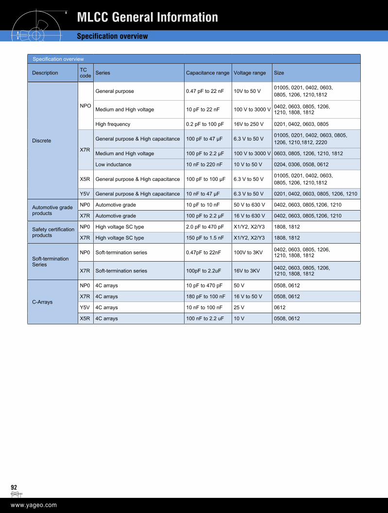
92
Specification overview
Description TC code Series Capacitance range Voltage range Size
Discrete
NPO
General purpose 0.47 pF to 22 nF 10V to 50 V01005, 0201, 0402, 0603, 0805, 1206, 1210,1812
Medium and High voltage 10 pF to 22 nF 100 V to 3000 V 0402, 0603, 0805, 1206, 1210, 1808, 1812
High frequency 0.2 pF to 100 pF 16V to 250 V 0201, 0402, 0603, 0805
X7R
General purpose & High capacitance 100 pF to 47 µF 6.3 V to 50 V01005, 0201, 0402, 0603, 0805, 1206, 1210,1812, 2220
Medium and High voltage 100 pF to 2.2 µF 100 V to 3000 V 0603, 0805, 1206, 1210, 1812
Low inductance 10 nF to 220 nF 10 V to 50 V 0204, 0306, 0508, 0612
X5R General purpose & High capacitance 100 pF to 100 µF 6.3 V to 50 V01005, 0201, 0402, 0603, 0805, 1206, 1210,1812
Y5V General purpose & High capacitance 10 nF to 47 µF 6.3 V to 50 V 0201, 0402, 0603, 0805, 1206, 1210
Automotive grade products
NP0 Automotive grade 10 pF to 10 nF 50 V to 630 V 0402, 0603, 0805,1206, 1210
X7R Automotive grade 100 pF to 2.2 μF 16 V to 630 V 0402, 0603, 0805,1206, 1210
Safety certification products
NP0 High voltage SC type 2.0 pF to 470 pF X1/Y2, X2/Y3 1808, 1812
X7R High voltage SC type 150 pF to 1.5 nF X1/Y2, X2/Y3 1808, 1812
Soft-termination Series
NP0 Soft-termination series 0.47pF to 22nF 100V to 3KV 0402, 0603, 0805, 1206, 1210, 1808, 1812
X7R Soft-termination series 100pF to 2.2uF 16V to 3KV 0402, 0603, 0805, 1206, 1210, 1808, 1812
C-Arrays
NP0 4C arrays 10 pF to 470 pF 50 V 0508, 0612
X7R 4C arrays 180 pF to 100 nF 16 V to 50 V 0508, 0612
Y5V 4C arrays 10 nF to 100 nF 25 V 0612
X5R 4C arrays 100 nF to 2.2 uF 10 V 0508, 0612
MLCC General InformationSpecification overview
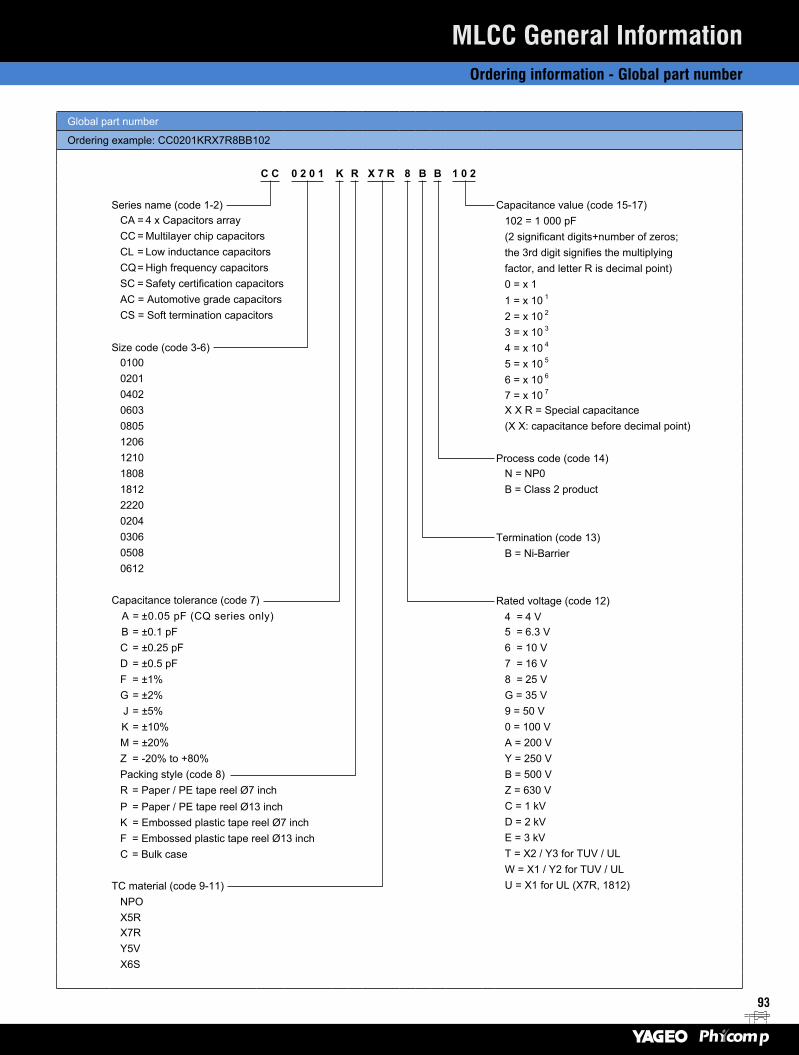
93
Global part number
Ordering example: CC0201KRX7R8BB102
C C 0 2 0 1 K R X 7 R 8 B B 1 0 2
Series name (code 1-2) Capacitance value (code 15-17) CA = 4 x Capacitors array 102 = 1 000 pF CC = Multilayer chip capacitors (2 significant digits+number of zeros; CL = Low inductance capacitors the 3rd digit signifies the multiplying CQ = High frequency capacitors factor, and letter R is decimal point) SC = Safety certification capacitors 0 = x 1AC = Automotive grade capacitors 1 = x 10 1
CS = Soft termination capacitors 2 = x 10 2
3 = x 10 3
Size code (code 3-6) 4 = x 10 4
0100 5 = x 10 5
0201 6 = x 10 6
0402 7 = x 10 7
0603 X X R = Special capacitance0805 (X X: capacitance before decimal point) 12061210 Process code (code 14)1808 N = NP01812 B = Class 2 product222002040306 Termination (code 13)0508 B = Ni-Barrier0612
Capacitance tolerance (code 7) Rated voltage (code 12) A = ±0.05 pF (CQ series only) 4 = 4 V B = ±0.1 pF 5 = 6.3 V C = ±0.25 pF 6 = 10 V D = ±0.5 pF 7 = 16 V F = ±1% 8 = 25 VG = ±2% G = 35 V J = ±5% 9 = 50 V K = ±10% 0 = 100 V M = ±20% A = 200 VZ = -20% to +80% Y = 250 V Packing style (code 8) B = 500 VR = Paper / PE tape reel Ø7 inch Z = 630 VP = Paper / PE tape reel Ø13 inch C = 1 kVK = Embossed plastic tape reel Ø7 inch D = 2 kVF = Embossed plastic tape reel Ø13 inch E = 3 kVC = Bulk case T = X2 / Y3 for TUV / UL
W = X1 / Y2 for TUV / ULTC material (code 9-11) U = X1 for UL (X7R, 1812)
NPOX5RX7RY5VX6S
MLCC General InformationOrdering information - Global part number
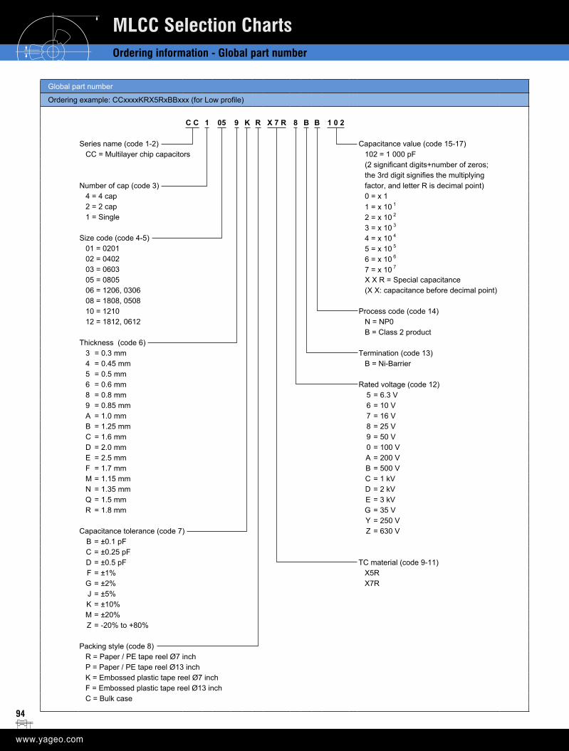
94
Global part number
Ordering example: CCxxxxKRX5RxBBxxx (for Low profile)
C C 1 05 9 K R X 7 R 8 B B 1 0 2
Series name (code 1-2) Capacitance value (code 15-17)CC = Multilayer chip capacitors 102 = 1 000 pF
(2 significant digits+number of zeros; the 3rd digit signifies the multiplying
Number of cap (code 3) factor, and letter R is decimal point)4 = 4 cap 0 = x 12 = 2 cap 1 = x 10 1
1 = Single 2 = x 10 2
3 = x 10 3
Size code (code 4-5) 4 = x 10 4
01 = 0201 5 = x 10 5
02 = 0402 6 = x 10 6
03 = 0603 7 = x 10 7
05 = 0805 X X R = Special capacitance06 = 1206, 0306 (X X: capacitance before decimal point) 08 = 1808, 0508 10 = 1210 Process code (code 14)12 = 1812, 0612 N = NP0
B = Class 2 productThickness (code 6)
3 = 0.3 mm Termination (code 13)4 = 0.45 mm B = Ni-Barrier5 = 0.5 mm 6 = 0.6 mm Rated voltage (code 12)8 = 0.8 mm 5 = 6.3 V 9 = 0.85 mm 6 = 10 V A = 1.0 mm 7 = 16 VB = 1.25 mm 8 = 25 VC = 1.6 mm 9 = 50 V D = 2.0 mm 0 = 100 VE = 2.5 mm A = 200 VF = 1.7 mm B = 500 VM = 1.15 mm C = 1 kVN = 1.35 mm D = 2 kVQ = 1.5 mm E = 3 kVR = 1.8 mm G = 35 V
Y = 250 VCapacitance tolerance (code 7) Z = 630 V
B = ±0.1 pF C = ±0.25 pF D = ±0.5 pF TC material (code 9-11) F = ±1% X5R G = ±2% X7R J = ±5% K = ±10% M = ±20% Z = -20% to +80%
Packing style (code 8)R = Paper / PE tape reel Ø7 inchP = Paper / PE tape reel Ø13 inchK = Embossed plastic tape reel Ø7 inchF = Embossed plastic tape reel Ø13 inchC = Bulk case
MLCC Selection ChartsOrdering information - Global part number
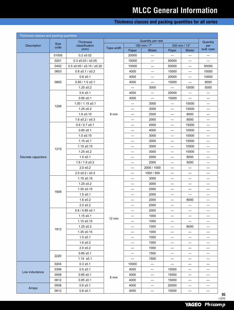
95
Thickness classes and packing quantities
Description Size code
Thickness classification
(mm)
Quantity per reel Quantity per
bulk caseTape width 180 mm / 7” 330 mm / 13”
Paper Blister Paper Blister
Discrete capacitors
01005 0.2 ±0.02
8 mm
20000 --- --- --- ---
0201 0.3 ±0.03 / ±0.05 15000 --- 50000 --- ---
0402 0.5 ±0.05 / ±0.15 / ±0.20 10000 --- 50000 --- 50000
0603 0.8 ±0.1 / ±0.2 4000 --- 15000 --- 15000
0805
0.6 ±0.1 4000 --- 20000 --- 10000
0.85 / 1.0 ±0.1 4000 --- 15000 --- 8000
1.25 ±0.2 --- 3000 --- 10000 5000
1206
0.6 ±0.1 4000 --- 20000 --- ---
0.85 ±0.1 4000 --- 15000 --- ---
1.00 / 1.15 ±0.1 --- 3000 --- 10000 ---
1.25 ±0.2 --- 3000 --- 10000 ---
1.6 ±0.15 --- 2500 --- 8000 ---
1.6 ±0.2 / ±0.3 --- 2000 --- 8000 ---
1210
0.6 / 0.7 ±0.1 --- 4000 --- 15000 ---
0.85 ±0.1 --- 4000 --- 10000 ---
1.0 ±0.15 --- 3000 --- 10000 ---
1.15 ±0.1 --- 3000 --- 10000 ---
1.15 ±0.15 --- 3000 --- 10000 ---
1.25 ±0.2 --- 3000 --- 10000 ---
1.5 ±0.1 --- 2000 --- 8000 ---
1.6 / 1.9 ±0.2 --- 2000 --- 5000 ---
2.0 ±0.2 --- 2000 / 1000 --- --- ---
2.5 ±0.2 / ±0.3 --- 1000 / 500 --- --- ---
1808
1.15 ±0.15
12 mm
--- 3000 --- --- ---
1.25 ±0.2 --- 3000 --- --- ---
1.35 ±0.15 --- 2000 --- --- ---
1.5 ±0.1 --- 2000 --- --- ---
1.6 ±0.2 --- 2000 --- 8000 ---
2.0 ±0.2 --- 2000 --- --- ---
1812
0.6 / 0.85 ±0.1 --- 2000 --- --- ---
1.15 ±0.1 --- 1000 --- --- ---
1.15 ±0.15 --- 1000 --- --- ---
1.25 ±0.2 --- 1000 --- 8000 ---
1.35 ±0.15 --- 1000 --- --- ---
1.5 ±0.1 --- 1000 --- --- ---
1.6 ±0.2 --- 1000 --- --- ---
2.0 ±0.2 --- 1000 --- --- ---
22200.85 ±0.1 --- 1500 --- --- ---
1.15 ±0.1 --- 1500 --- --- ---
Low inductance
0204 0.3 ±0.1
8 mm
10000 --- --- --- ---
0306 0.5 ±0.1 4000 --- 15000 --- ---
0508 0.85 ±0.1 4000 --- 15000 --- ---
0612 0.85 ±0.1 4000 --- 15000 --- ---
Arrays0508 0.6 ±0.1 4000 --- 20000 --- ---
0612 0.8 ±0.1 4000 --- 15000 --- ---
MLCC General InformationThickness classes and packing quantities for all series
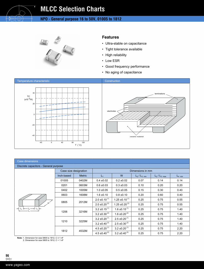
96
MLCC Selection ChartsNPO - General purpose 16 to 50V, 01005 to 1812
Temperature characteristic Construction
Case dimensions
Discrete capacitors - General purpose
L2 L3L4L1
W
Case size designation Dimensions in mm
Inch-based Metric L1 W L2 / L3 min L2 / L3 max L4 min
01005 0402M 0.4 ±0.02 0.2 ±0.02 0.07 0.14 0.14
0201 0603M 0.6 ±0.03 0.3 ±0.03 0.10 0.20 0.20
0402 1005M 1.0 ±0.05 0.5 ±0.05 0.15 0.30 0.40
0603 1608M 1.6 ±0.10 0.8 ±0.10 0.20 0.60 0.40
0805 2012M 2.0 ±0.10
(1) 1.25 ±0.10 (1) 0.25 0.75 0.55
2.0 ±0.20 (2) 1.25 ±0.20 (2) 0.25 0.75 0.55
1206 3216M 3.2 ±0.15 (1) 1.6 ±0.15 (1) 0.25 0.75 1.40
3.2 ±0.30 (2) 1.6 ±0.20 (2) 0.25 0.75 1.40
1210 3225M 3.2 ±0.20 (1) 2.5 ±0.20 (1) 0.25 0.75 1.40
3.2 ±0.40 (2) 2.5 ±0.30 (2) 0.25 0.75 1.40
1812 4532M 4.5 ±0.20 (1) 3.2 ±0.20 (1) 0.25 0.75 2.20
4.5 ±0.40 (2) 3.2 ±0.40 (2) 0.25 0.75 2.20
Note: 1. Dimension for size 0805 to 1812, C ≤ 1 nF 2. Dimension for size 0805 to 1812, C > 1 nF
Features• Ultra-stable on capacitance
• Tight tolerance available
• High reliability
• Low ESR
• Good frequency performance
• No aging of capacitance
40
0
20
0 40 80 120T ( C)
TC(x10 /K)- 6
-40
-40
-20
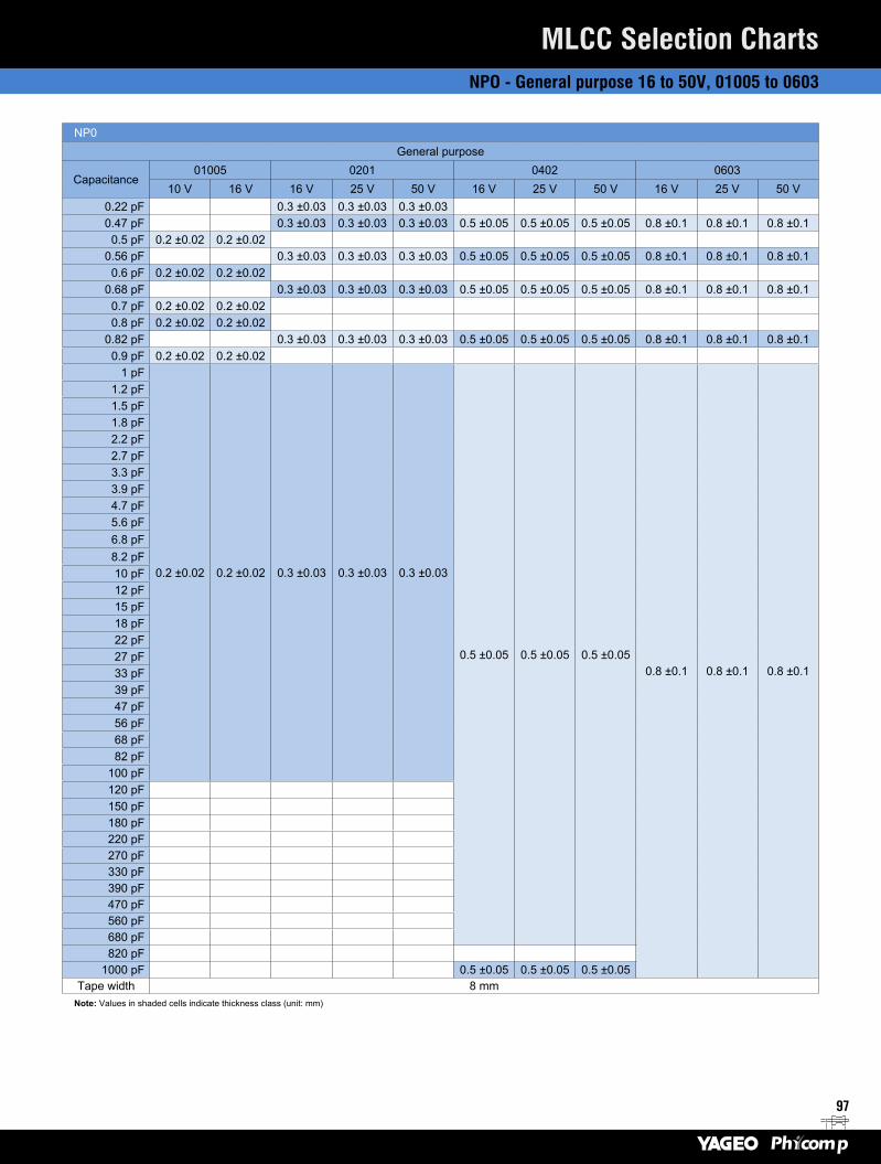
97
MLCC Selection ChartsNPO - General purpose 16 to 50V, 01005 to 0603
NP0General purpose
Capacitance01005 0201 0402 0603
10 V 16 V 16 V 25 V 50 V 16 V 25 V 50 V 16 V 25 V 50 V0.22 pF 0.3 ±0.03 0.3 ±0.03 0.3 ±0.030.47 pF 0.3 ±0.03 0.3 ±0.03 0.3 ±0.03 0.5 ±0.05 0.5 ±0.05 0.5 ±0.05 0.8 ±0.1 0.8 ±0.1 0.8 ±0.1
0.5 pF 0.2 ±0.02 0.2 ±0.020.56 pF 0.3 ±0.03 0.3 ±0.03 0.3 ±0.03 0.5 ±0.05 0.5 ±0.05 0.5 ±0.05 0.8 ±0.1 0.8 ±0.1 0.8 ±0.1
0.6 pF 0.2 ±0.02 0.2 ±0.020.68 pF 0.3 ±0.03 0.3 ±0.03 0.3 ±0.03 0.5 ±0.05 0.5 ±0.05 0.5 ±0.05 0.8 ±0.1 0.8 ±0.1 0.8 ±0.1
0.7 pF 0.2 ±0.02 0.2 ±0.020.8 pF 0.2 ±0.02 0.2 ±0.02
0.82 pF 0.3 ±0.03 0.3 ±0.03 0.3 ±0.03 0.5 ±0.05 0.5 ±0.05 0.5 ±0.05 0.8 ±0.1 0.8 ±0.1 0.8 ±0.10.9 pF 0.2 ±0.02 0.2 ±0.02
1 pF
0.2 ±0.02 0.2 ±0.02 0.3 ±0.03 0.3 ±0.03 0.3 ±0.03
0.5 ±0.05 0.5 ±0.05 0.5 ±0.050.8 ±0.1 0.8 ±0.1 0.8 ±0.1
1.2 pF1.5 pF1.8 pF2.2 pF2.7 pF3.3 pF3.9 pF4.7 pF5.6 pF6.8 pF8.2 pF10 pF12 pF15 pF18 pF22 pF27 pF33 pF39 pF47 pF56 pF68 pF82 pF
100 pF120 pF150 pF180 pF220 pF270 pF330 pF390 pF470 pF560 pF680 pF820 pF
1000 pF 0.5 ±0.05 0.5 ±0.05 0.5 ±0.05Tape width 8 mm
Note: Values in shaded cells indicate thickness class (unit: mm)
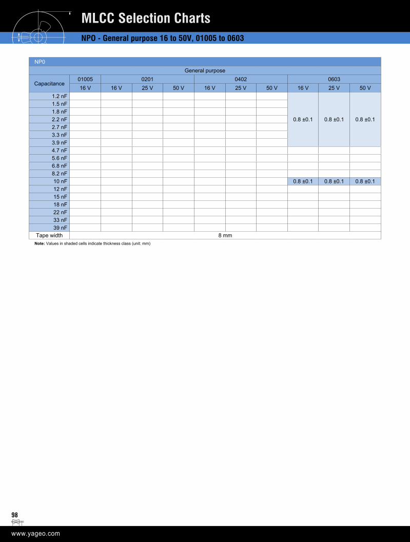
98
MLCC Selection ChartsNPO - General purpose 16 to 50V, 01005 to 0603
NP0General purpose
Capacitance01005 0201 0402 060316 V 16 V 25 V 50 V 16 V 25 V 50 V 16 V 25 V 50 V
1.2 nF
0.8 ±0.1 0.8 ±0.1 0.8 ±0.1
1.5 nF1.8 nF2.2 nF2.7 nF3.3 nF3.9 nF4.7 nF5.6 nF6.8 nF8.2 nF10 nF 0.8 ±0.1 0.8 ±0.1 0.8 ±0.112 nF15 nF18 nF22 nF33 nF39 nF
Tape width 8 mmNote: Values in shaded cells indicate thickness class (unit: mm)
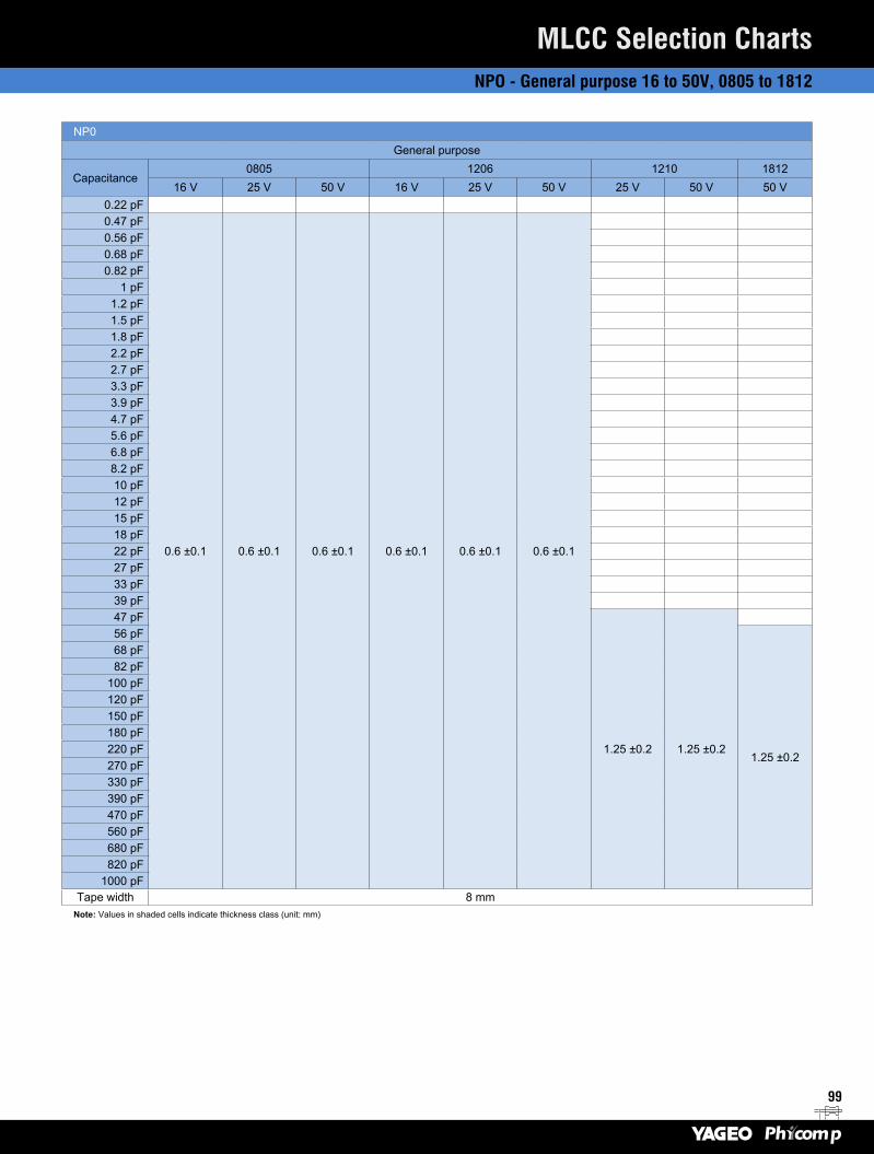
99
NPO - General purpose 16 to 50V, 0805 to 1812
MLCC Selection Charts
NP0General purpose
Capacitance0805 1206 1210 1812
16 V 25 V 50 V 16 V 25 V 50 V 25 V 50 V 50 V0.22 pF0.47 pF
0.6 ±0.1 0.6 ±0.1 0.6 ±0.1 0.6 ±0.1 0.6 ±0.1 0.6 ±0.1
0.56 pF0.68 pF0.82 pF
1 pF1.2 pF1.5 pF1.8 pF2.2 pF2.7 pF3.3 pF3.9 pF4.7 pF5.6 pF6.8 pF8.2 pF10 pF12 pF15 pF18 pF22 pF27 pF33 pF39 pF47 pF
1.25 ±0.2 1.25 ±0.2
56 pF
1.25 ±0.2
68 pF82 pF
100 pF120 pF150 pF180 pF220 pF270 pF330 pF390 pF470 pF560 pF680 pF820 pF
1000 pFTape width 8 mm
Note: Values in shaded cells indicate thickness class (unit: mm)
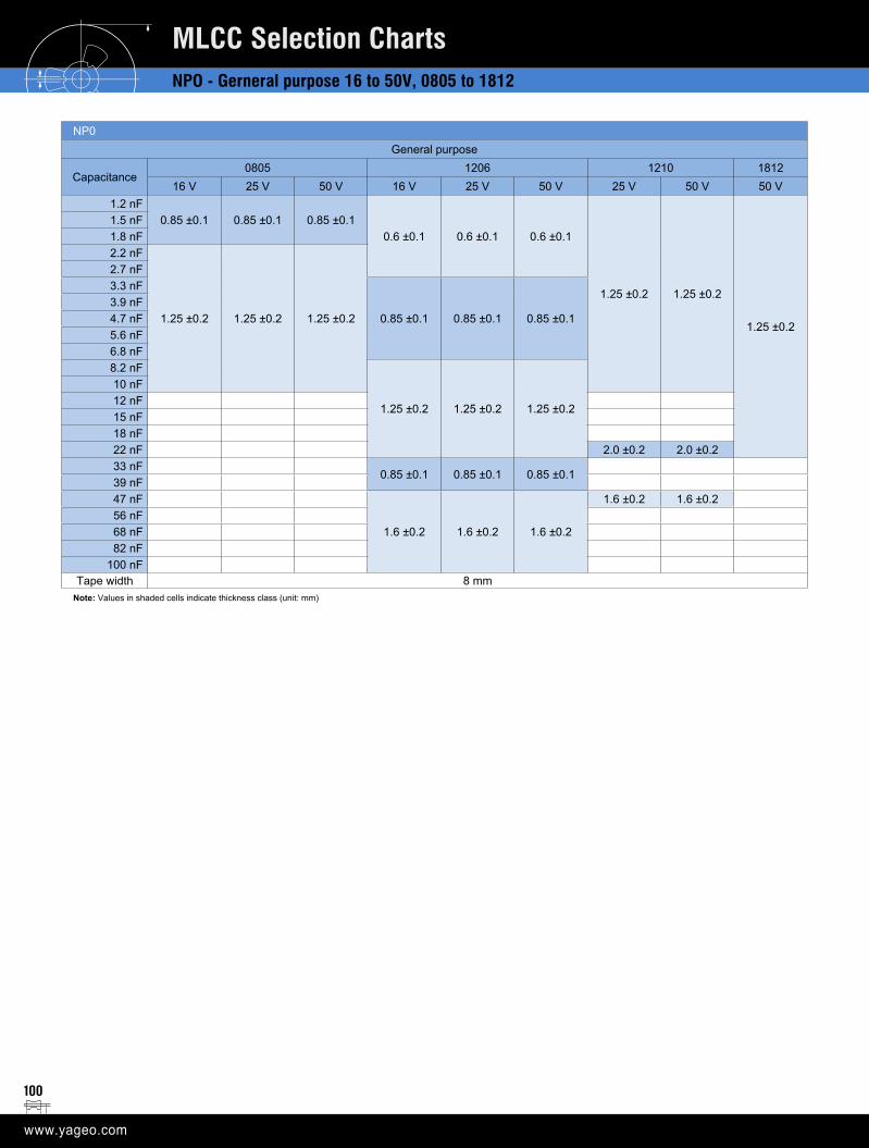
100
NPO - Gerneral purpose 16 to 50V, 0805 to 1812
MLCC Selection Charts
NP0General purpose
Capacitance0805 1206 1210 1812
16 V 25 V 50 V 16 V 25 V 50 V 25 V 50 V 50 V1.2 nF
0.85 ±0.1 0.85 ±0.1 0.85 ±0.10.6 ±0.1 0.6 ±0.1 0.6 ±0.1
1.25 ±0.2 1.25 ±0.2
1.25 ±0.2
1.5 nF1.8 nF2.2 nF
1.25 ±0.2 1.25 ±0.2 1.25 ±0.2
2.7 nF3.3 nF
0.85 ±0.1 0.85 ±0.1 0.85 ±0.13.9 nF4.7 nF5.6 nF6.8 nF8.2 nF
1.25 ±0.2 1.25 ±0.2 1.25 ±0.2
10 nF12 nF15 nF18 nF22 nF 2.0 ±0.2 2.0 ±0.233 nF
0.85 ±0.1 0.85 ±0.1 0.85 ±0.139 nF47 nF
1.6 ±0.2 1.6 ±0.2 1.6 ±0.2
1.6 ±0.2 1.6 ±0.256 nF68 nF82 nF
100 nFTape width 8 mm
Note: Values in shaded cells indicate thickness class (unit: mm)
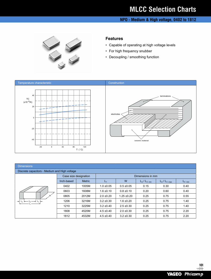
101
NPO - Medium & High voltage, 0402 to 1812
MLCC Selection Charts
Temperature characteristic Construction
Dimensions
Discrete capacitors - Medium and High voltage
L2 L3L4L1
W
Case size designation Dimensions in mm
Inch-based Metric L1 W L2 / L3 min L2 / L3 max L4 min
0402 1005M 1.0 ±0.05 0.5 ±0.05 0.15 0.30 0.40
0603 1608M 1.6 ±0.10 0.8 ±0.10 0.20 0.60 0.40
0805 2012M 2.0 ±0.20 1.25 ±0.20 0.25 0.75 0.55
1206 3216M 3.2 ±0.30 1.6 ±0.20 0.25 0.75 1.40
1210 3225M 3.2 ±0.40 2.5 ±0.30 0.25 0.75 1.40
1808 4520M 4.5 ±0.40 2.0 ±0.30 0.25 0.75 2.20
1812 4532M 4.5 ±0.40 3.2 ±0.30 0.25 0.75 2.20
Features• Capable of operating at high voltage levels
• For high frequency snubber
• Decoupling / smoothing function
40
0
20
0 40 80 120T ( C)
TC(x10 /K)- 6
-40
-40
-20
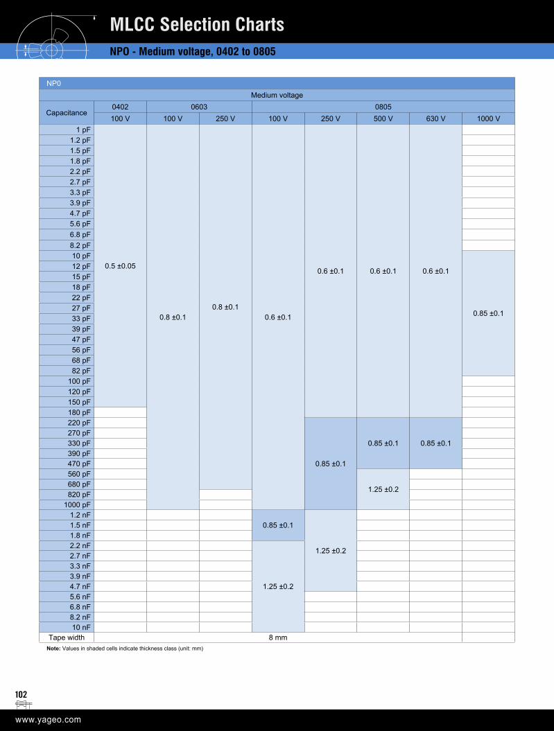
102
NPO - Medium voltage, 0402 to 0805
MLCC Selection Charts
NP0Medium voltage
Capacitance0402 0603 0805100 V 100 V 250 V 100 V 250 V 500 V 630 V 1000 V
1 pF
0.5 ±0.05
0.8 ±0.10.8 ±0.1
0.6 ±0.1
0.6 ±0.1 0.6 ±0.1 0.6 ±0.1
1.2 pF1.5 pF1.8 pF2.2 pF2.7 pF3.3 pF3.9 pF4.7 pF5.6 pF6.8 pF8.2 pF10 pF
0.85 ±0.1
12 pF15 pF18 pF22 pF27 pF33 pF39 pF47 pF56 pF68 pF82 pF
100 pF120 pF150 pF180 pF220 pF
0.85 ±0.1
0.85 ±0.1 0.85 ±0.1270 pF330 pF390 pF470 pF560 pF
1.25 ±0.2680 pF820 pF
1000 pF1.2 nF
0.85 ±0.1
1.25 ±0.2
1.5 nF1.8 nF2.2 nF
1.25 ±0.2
2.7 nF3.3 nF3.9 nF4.7 nF5.6 nF6.8 nF8.2 nF10 nF
Tape width 8 mmNote: Values in shaded cells indicate thickness class (unit: mm)
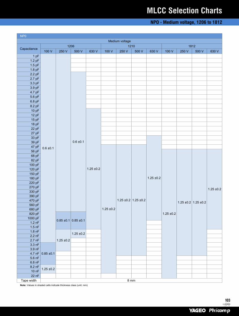
103
NPO - Medium voltage, 1206 to 1812
MLCC Selection Charts
NP0Medium voltage
Capacitance1206 1210 1812
100 V 250 V 500 V 630 V 100 V 250 V 500 V 630 V 100 V 250 V 500 V 630 V1 pF
0.6 ±0.1
1.2 pF1.5 pF1.8 pF2.2 pF
0.6 ±0.1
2.7 pF3.3 pF3.9 pF4.7 pF5.6 pF6.8 pF8.2 pF10 pF
1.25 ±0.2
12 pF15 pF18 pF22 pF27 pF33 pF
1.25 ±0.2
39 pF47 pF
1.25 ±0.2
1.25 ±0.2 1.25 ±0.2
56 pF
1.25 ±0.2
1.25 ±0.2 1.25 ±0.2
1.25 ±0.2
68 pF82 pF
100 pF120 pF150 pF180 pF220 pF270 pF330 pF390 pF470 pF560 pF680 pF820 pF
0.85 ±0.1 0.85 ±0.11000 pF
1.2 nF1.5 nF1.8 nF
1.25 ±0.2
1.25 ±0.22.2 nF2.7 nF3.3 nF
0.85 ±0.13.9 nF4.7 nF5.6 nF6.8 nF8.2 nF
1.25 ±0.210 nF22 nF
Tape width 8 mmNote: Values in shaded cells indicate thickness class (unit: mm)
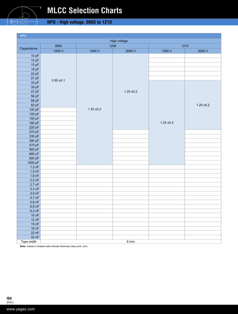
104
NP0High voltage
Capacitance0805 1206 1210
1000 V 1000 V 2000 V 1000 V 2000 V10 pF
0.85 ±0.1
1.25 ±0.2
1.25 ±0.2
12 pF15 pF18 pF22 pF27 pF33 pF
1.25 ±0.2
1.25 ±0.2
39 pF47 pF56 pF68 pF82 pF
100 pF120 pF150 pF180 pF220 pF270 pF330 pF390 pF470 pF560 pF680 pF820 pF
1000 pF1.2 nF1.5 nF1.8 nF2.2 nF2.7 nF3.3 nF3.9 nF4.7 nF5.6 nF6.8 nF8.2 nF10 nF12 nF15 nF18 nF22 nF33 nF
Tape width 8 mmNote: Values in shaded cells indicate thickness class (unit: mm)
NPO - High voltage, 0805 to 1210
MLCC Selection Charts
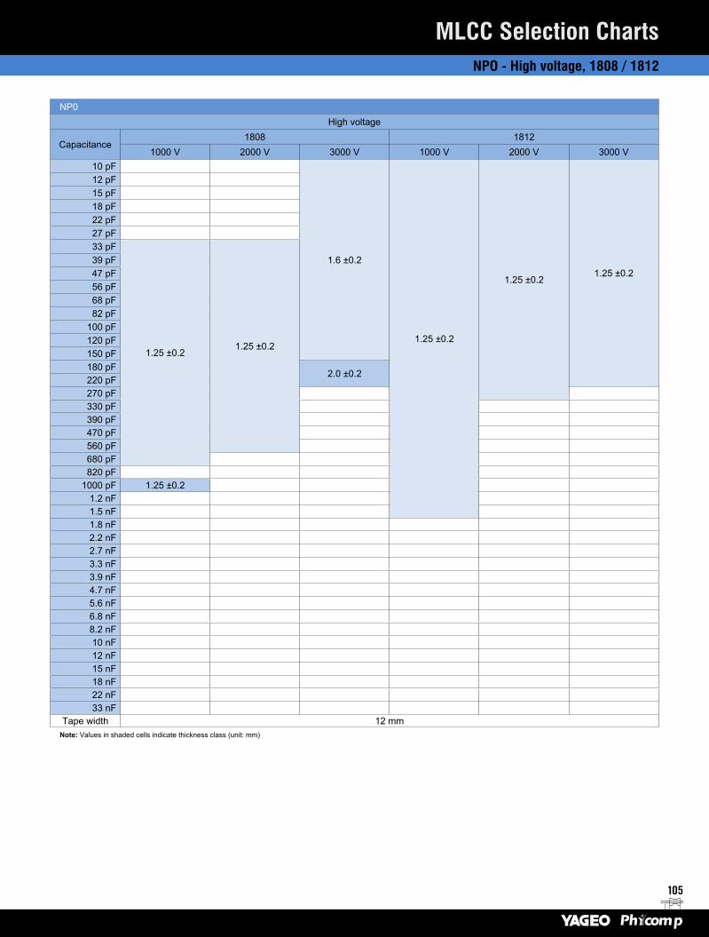
105
NP0High voltage
Capacitance1808 1812
1000 V 2000 V 3000 V 1000 V 2000 V 3000 V10 pF
1.6 ±0.2
1.25 ±0.2
1.25 ±0.21.25 ±0.2
12 pF15 pF18 pF22 pF27 pF33 pF
1.25 ±0.21.25 ±0.2
39 pF47 pF56 pF68 pF82 pF
100 pF120 pF150 pF180 pF
2.0 ±0.2220 pF270 pF330 pF390 pF470 pF560 pF680 pF820 pF
1000 pF 1.25 ±0.21.2 nF1.5 nF1.8 nF2.2 nF2.7 nF3.3 nF3.9 nF4.7 nF5.6 nF6.8 nF8.2 nF10 nF12 nF15 nF18 nF22 nF33 nF
Tape width 12 mmNote: Values in shaded cells indicate thickness class (unit: mm)
NPO - High voltage, 1808 / 1812
MLCC Selection Charts
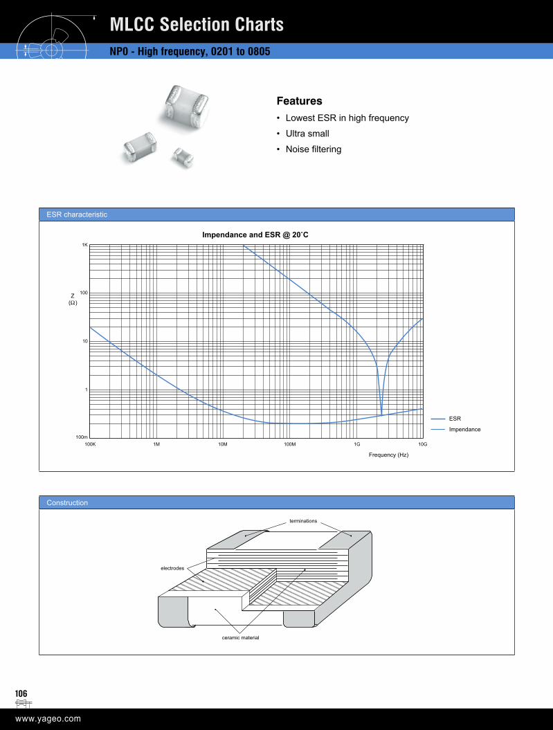
106
ESR characteristic
Construction
NP0 - High frequency, 0201 to 0805
MLCC Selection Charts
Features• Lowest ESR in high frequency
• Ultra small
• Noise filtering
Impendance and ESR @ 20 C
ESR
Impendance
Frequency (Hz)
100K 1M 10M 100M 1G 10G100m
1
10
100
1K
Z(Ω)
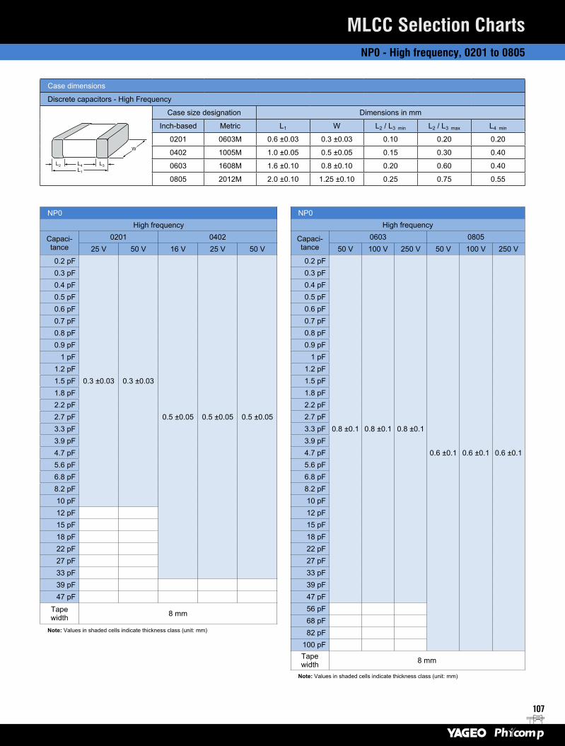
107
NP0 - High frequency, 0201 to 0805
MLCC Selection Charts
Case dimensions
Discrete capacitors - High Frequency
L2 L3L4L1
W
Case size designation Dimensions in mm
Inch-based Metric L1 W L2 / L3 min L2 / L3 max L4 min
0201 0603M 0.6 ±0.03 0.3 ±0.03 0.10 0.20 0.20
0402 1005M 1.0 ±0.05 0.5 ±0.05 0.15 0.30 0.40
0603 1608M 1.6 ±0.10 0.8 ±0.10 0.20 0.60 0.40
0805 2012M 2.0 ±0.10 1.25 ±0.10 0.25 0.75 0.55
NP0High frequency
Capaci-tance
0201 040225 V 50 V 16 V 25 V 50 V
0.2 pF
0.3 ±0.03 0.3 ±0.03
0.5 ±0.05 0.5 ±0.05 0.5 ±0.05
0.3 pF0.4 pF0.5 pF0.6 pF0.7 pF0.8 pF0.9 pF
1 pF1.2 pF1.5 pF1.8 pF2.2 pF2.7 pF3.3 pF3.9 pF4.7 pF5.6 pF6.8 pF8.2 pF10 pF12 pF15 pF18 pF22 pF27 pF33 pF39 pF47 pF
Tape width 8 mm
Note: Values in shaded cells indicate thickness class (unit: mm)
NP0High frequency
Capaci-tance
0603 080550 V 100 V 250 V 50 V 100 V 250 V
0.2 pF
0.8 ±0.1 0.8 ±0.1 0.8 ±0.1
0.6 ±0.1 0.6 ±0.1 0.6 ±0.1
0.3 pF0.4 pF0.5 pF0.6 pF0.7 pF0.8 pF0.9 pF
1 pF1.2 pF1.5 pF1.8 pF2.2 pF2.7 pF3.3 pF3.9 pF4.7 pF5.6 pF6.8 pF8.2 pF10 pF12 pF15 pF18 pF22 pF27 pF33 pF39 pF47 pF56 pF68 pF82 pF
100 pFTape width 8 mm
Note: Values in shaded cells indicate thickness class (unit: mm)
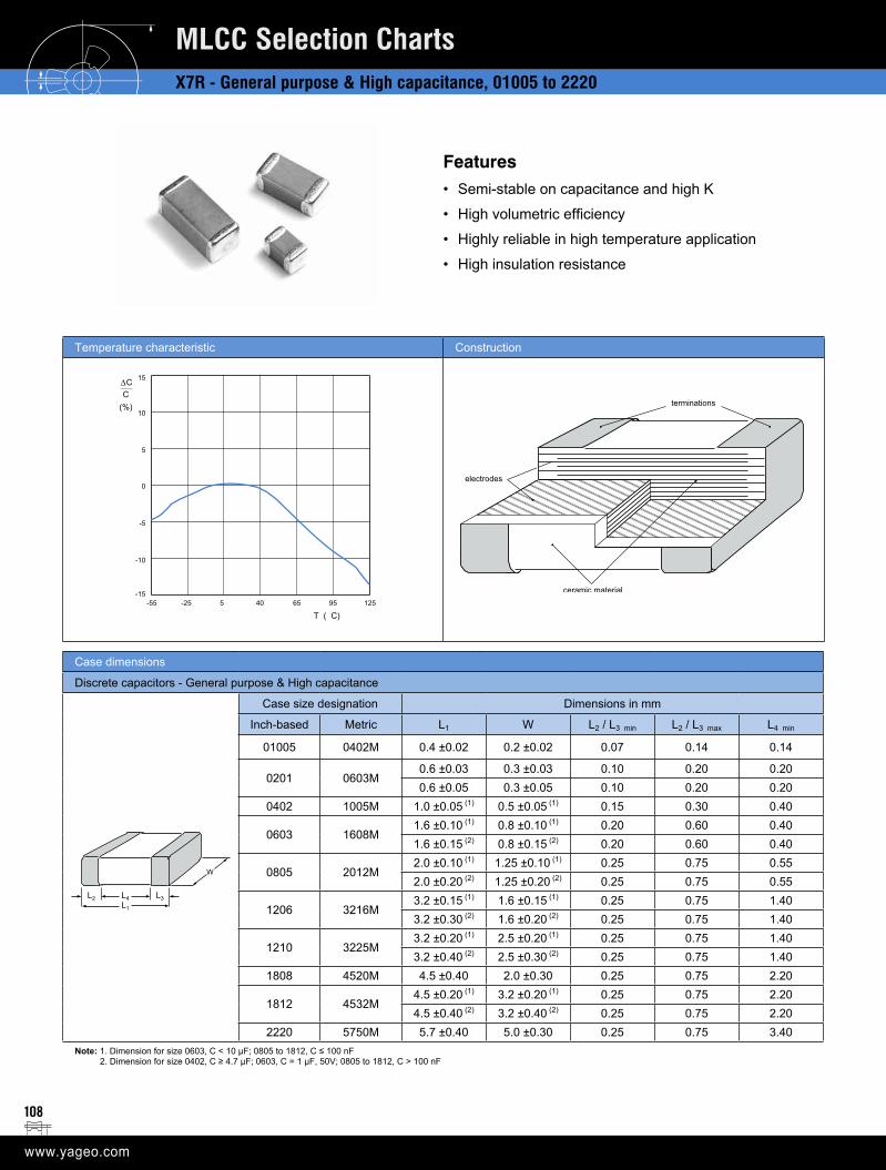
108
X7R - General purpose & High capacitance, 01005 to 2220
MLCC Selection Charts
Temperature characteristic Construction
Case dimensions
Discrete capacitors - General purpose & High capacitance
L2 L3L4L1
W
Case size designation Dimensions in mm
Inch-based Metric L1 W L2 / L3 min L2 / L3 max L4 min
01005 0402M 0.4 ±0.02 0.2 ±0.02 0.07 0.14 0.14
0201 0603M0.6 ±0.03 0.3 ±0.03 0.10 0.20 0.200.6 ±0.05 0.3 ±0.05 0.10 0.20 0.20
0402 1005M 1.0 ±0.05 (1) 0.5 ±0.05 (1) 0.15 0.30 0.40
0603 1608M1.6 ±0.10 (1) 0.8 ±0.10 (1) 0.20 0.60 0.401.6 ±0.15 (2) 0.8 ±0.15 (2) 0.20 0.60 0.40
0805 2012M2.0 ±0.10 (1) 1.25 ±0.10 (1) 0.25 0.75 0.552.0 ±0.20 (2) 1.25 ±0.20 (2) 0.25 0.75 0.55
1206 3216M3.2 ±0.15 (1) 1.6 ±0.15 (1) 0.25 0.75 1.403.2 ±0.30 (2) 1.6 ±0.20 (2) 0.25 0.75 1.40
1210 3225M3.2 ±0.20 (1) 2.5 ±0.20 (1) 0.25 0.75 1.403.2 ±0.40 (2) 2.5 ±0.30 (2) 0.25 0.75 1.40
1808 4520M 4.5 ±0.40 2.0 ±0.30 0.25 0.75 2.20
1812 4532M4.5 ±0.20 (1) 3.2 ±0.20 (1) 0.25 0.75 2.204.5 ±0.40 (2) 3.2 ±0.40 (2) 0.25 0.75 2.20
2220 5750M 5.7 ±0.40 5.0 ±0.30 0.25 0.75 3.40Note: 1. Dimension for size 0603, C < 10 μF; 0805 to 1812, C ≤ 100 nF 2. Dimension for size 0402, C ≥ 4.7 μF; 0603, C = 1 μF, 50V; 0805 to 1812, C > 100 nF
Features• Semi-stable on capacitance and high K
• High volumetric efficiency
• Highly reliable in high temperature application
• High insulation resistance
15
5
-15-25-55 5 40 9565 125
10
-10
∆CC
(%)
-5
0
T ( C)
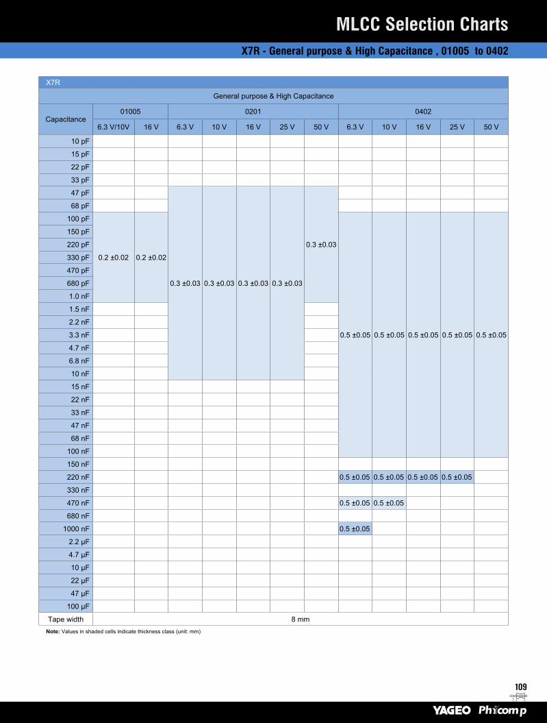
109
X7R - General purpose & High Capacitance , 01005 to 0402
MLCC Selection Charts
X7R
General purpose & High Capacitance
Capacitance01005 0201 0402
6.3 V/10V 16 V 6.3 V 10 V 16 V 25 V 50 V 6.3 V 10 V 16 V 25 V 50 V
10 pF
15 pF
22 pF
33 pF
47 pF
0.3 ±0.03 0.3 ±0.03 0.3 ±0.03 0.3 ±0.03
0.3 ±0.03
68 pF
100 pF
0.2 ±0.02 0.2 ±0.02
0.5 ±0.05 0.5 ±0.05 0.5 ±0.05 0.5 ±0.05 0.5 ±0.05
150 pF
220 pF
330 pF
470 pF
680 pF
1.0 nF
1.5 nF
2.2 nF
3.3 nF
4.7 nF
6.8 nF
10 nF
15 nF
22 nF
33 nF
47 nF
68 nF
100 nF
150 nF
220 nF 0.5 ±0.05 0.5 ±0.05 0.5 ±0.05 0.5 ±0.05
330 nF
470 nF 0.5 ±0.05 0.5 ±0.05
680 nF
1000 nF 0.5 ±0.05
2.2 μF
4.7 μF
10 μF
22 μF
47 μF
100 μF
Tape width 8 mmNote: Values in shaded cells indicate thickness class (unit: mm)
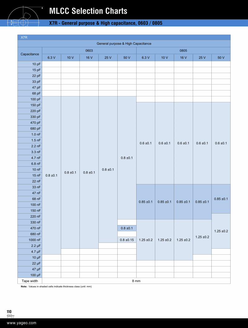
110
X7R - General purpose & High capacitance, 0603 / 0805
MLCC Selection Charts
X7R
General purpose & High Capacitance
Capacitance0603 0805
6.3 V 10 V 16 V 25 V 50 V 6.3 V 10 V 16 V 25 V 50 V
10 pF
15 pF
22 pF
33 pF
47 pF
68 pF
100 pF
0.8 ±0.10.8 ±0.1 0.8 ±0.1
0.8 ±0.1
0.8 ±0.1
150 pF
0.6 ±0.1 0.6 ±0.1 0.6 ±0.1 0.6 ±0.1 0.6 ±0.1
220 pF
330 pF
470 pF
680 pF
1.0 nF
1.5 nF
2.2 nF
3.3 nF
4.7 nF
6.8 nF
10 nF
15 nF
22 nF
33 nF
0.85 ±0.1 0.85 ±0.1 0.85 ±0.1 0.85 ±0.10.85 ±0.1
47 nF
68 nF
100 nF
150 nF
220 nF
1.25 ±0.2
330 nF
1.25 ±0.2 1.25 ±0.2 1.25 ±0.21.25 ±0.2
470 nF 0.8 ±0.1
680 nF
1000 nF 0.8 ±0.15
2.2 μF
4.7 μF
10 μF
22 μF
47 μF
100 μF
Tape width 8 mmNote: Values in shaded cells indicate thickness class (unit: mm)
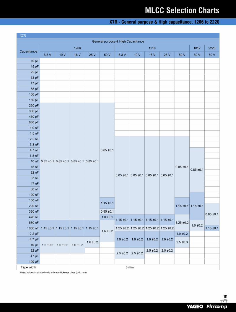
111
X7R - General purpose & High capacitance, 1206 to 2220
MLCC Selection Charts
X7R
General purpose & High Capacitance
Capacitance1206 1210 1812 2220
6.3 V 10 V 16 V 25 V 50 V 6.3 V 10 V 16 V 25 V 50 V 50 V 50 V
10 pF
15 pF
22 pF
33 pF
47 pF
68 pF
100 pF
150 pF
220 pF
0.85 ±0.1 0.85 ±0.1 0.85 ±0.1 0.85 ±0.1
0.85 ±0.1
330 pF
470 pF
680 pF
1.0 nF
1.5 nF
2.2 nF
0.85 ±0.1 0.85 ±0.1 0.85 ±0.1 0.85 ±0.1
0.85 ±0.1
3.3 nF
4.7 nF
0.85 ±0.1
6.8 nF
10 nF
15 nF
22 nF
33 nF
47 nF
68 nF
100 nF
1.15 ±0.1
150 nF1.15 ±0.1
1.15 ±0.1220 nF
0.85 ±0.1330 nF 0.85 ±0.1
470 nF 1.0 ±0.11.15 ±0.1 1.15 ±0.1 1.15 ±0.1 1.15 ±0.1
1.25 ±0.2680 nF
1.15 ±0.1 1.15 ±0.1 1.15 ±0.1 1.15 ±0.11.6 ±0.2
1.6 ±0.21000 nF 1.25 ±0.2 1.25 ±0.2 1.25 ±0.2 1.25 ±0.2 1.15 ±0.1
2.2 μF
1.9 ±0.2 1.9 ±0.2 1.9 ±0.2 1.9 ±0.2
1.9 ±0.2
4.7 μF
1.6 ±0.2 1.6 ±0.2 1.6 ±0.21.6 ±0.2 2.5 ±0.3
10 μF
22 μF2.5 ±0.2 2.5 ±0.2
2.5 ±0.2 2.5 ±0.2
47 μF
100 μF
Tape width 8 mmNote: Values in shaded cells indicate thickness class (unit: mm)
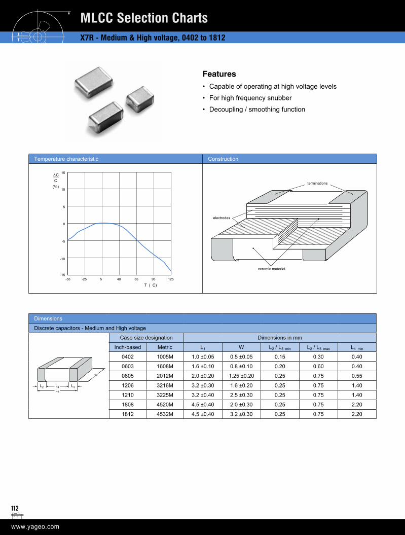
112
X7R - Medium & High voltage, 0402 to 1812
MLCC Selection Charts
Temperature characteristic Construction
Dimensions
Discrete capacitors - Medium and High voltage
L2 L3L4L1
W
Case size designation Dimensions in mm
Inch-based Metric L1 W L2 / L3 min L2 / L3 max L4 min
0402 1005M 1.0 ±0.05 0.5 ±0.05 0.15 0.30 0.40
0603 1608M 1.6 ±0.10 0.8 ±0.10 0.20 0.60 0.40
0805 2012M 2.0 ±0.20 1.25 ±0.20 0.25 0.75 0.55
1206 3216M 3.2 ±0.30 1.6 ±0.20 0.25 0.75 1.40
1210 3225M 3.2 ±0.40 2.5 ±0.30 0.25 0.75 1.40
1808 4520M 4.5 ±0.40 2.0 ±0.30 0.25 0.75 2.20
1812 4532M 4.5 ±0.40 3.2 ±0.30 0.25 0.75 2.20
Features• Capable of operating at high voltage levels
• For high frequency snubber
• Decoupling / smoothing function
15
5
-15-25-55 5 40 9565 125
10
-10
∆CC
(%)
-5
0
T ( C)
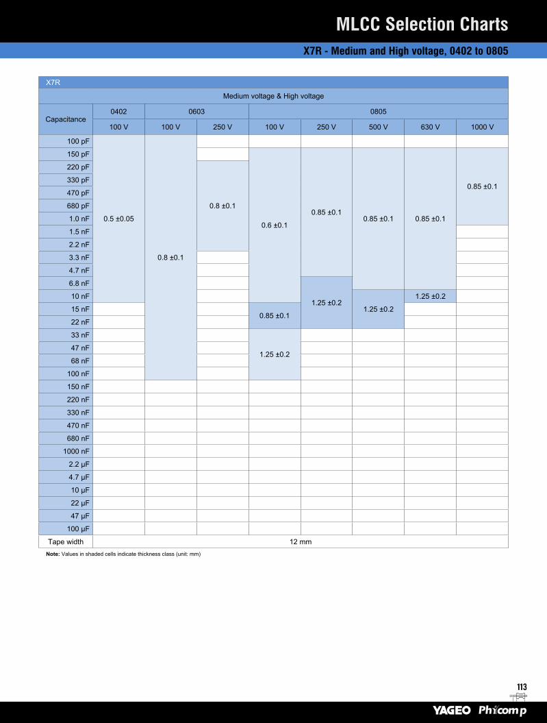
113
X7R - Medium and High voltage, 0402 to 0805
MLCC Selection Charts
X7R
Medium voltage & High voltage
Capacitance0402 0603 0805
100 V 100 V 250 V 100 V 250 V 500 V 630 V 1000 V
100 pF
0.5 ±0.05
0.8 ±0.1
150 pF
0.6 ±0.1
0.85 ±0.10.85 ±0.1 0.85 ±0.1
0.85 ±0.1
220 pF
0.8 ±0.1
330 pF
470 pF
680 pF
1.0 nF
1.5 nF
2.2 nF
3.3 nF
4.7 nF
6.8 nF
1.25 ±0.210 nF
1.25 ±0.2
1.25 ±0.2
15 nF0.85 ±0.1
22 nF
33 nF
1.25 ±0.247 nF
68 nF
100 nF
150 nF
220 nF
330 nF
470 nF
680 nF
1000 nF
2.2 μF
4.7 μF
10 μF
22 μF
47 μF
100 μF
Tape width 12 mmNote: Values in shaded cells indicate thickness class (unit: mm)
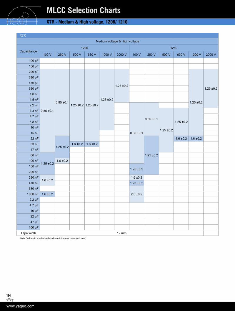
114
X7R
Medium voltage & High voltage
Capacitance1206 1210
100 V 250 V 500 V 630 V 1000 V 2000 V 100 V 250 V 500 V 630 V 1000 V 2000 V
100 pF
150 pF
220 pF
0.85 ±0.1
0.85 ±0.11.25 ±0.2 1.25 ±0.2
1.25 ±0.2
1.25 ±0.2
1.25 ±0.2
1.25 ±0.2
330 pF
470 pF
680 pF
1.0 nF
1.5 nF
2.2 nF
0.85 ±0.1
0.85 ±0.1
3.3 nF
1.25 ±0.2
1.25 ±0.2
4.7 nF
6.8 nF
10 nF
15 nF
22 nF
1.25 ±0.2
1.25 ±0.2
1.6 ±0.2 1.6 ±0.2
33 nF 1.6 ±0.2 1.6 ±0.2
47 nF
68 nF
1.25 ±0.2100 nF 1.6 ±0.2
150 nF1.25 ±0.2
220 nF
330 nF1.6 ±0.2
1.6 ±0.2
470 nF 1.25 ±0.2
680 nF
2.0 ±0.21000 nF 1.6 ±0.2
2.2 μF
4.7 μF
10 μF
22 μF
47 μF
100 μF
Tape width 12 mmNote: Values in shaded cells indicate thickness class (unit: mm)
MLCC Selection ChartsX7R - Medium & High voltage, 1206/ 1210
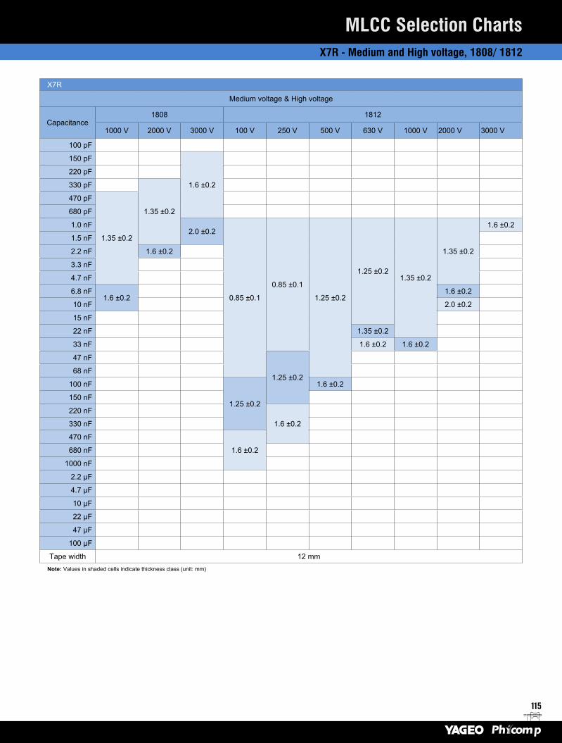
115
X7R
Medium voltage & High voltage
Capacitance1808 1812
1000 V 2000 V 3000 V 100 V 250 V 500 V 630 V 1000 V 2000 V 3000 V
100 pF
150 pF
1.6 ±0.2
220 pF
330 pF
1.35 ±0.2
470 pF
1.35 ±0.2
680 pF
1.0 nF2.0 ±0.2
0.85 ±0.1
0.85 ±0.1
1.25 ±0.2
1.25 ±0.21.35 ±0.2
1.35 ±0.2
1.6 ±0.2
1.5 nF
2.2 nF 1.6 ±0.2
3.3 nF
4.7 nF
6.8 nF1.6 ±0.2
1.6 ±0.2
10 nF 2.0 ±0.2
15 nF
22 nF 1.35 ±0.2
33 nF 1.6 ±0.2 1.6 ±0.2
47 nF
1.25 ±0.268 nF
100 nF
1.25 ±0.2
1.6 ±0.2
150 nF
220 nF
1.6 ±0.2330 nF
470 nF
1.6 ±0.2680 nF
1000 nF
2.2 μF
4.7 μF
10 μF
22 μF
47 μF
100 μF
Tape width 12 mmNote: Values in shaded cells indicate thickness class (unit: mm)
X7R - Medium and High voltage, 1808/ 1812
MLCC Selection Charts
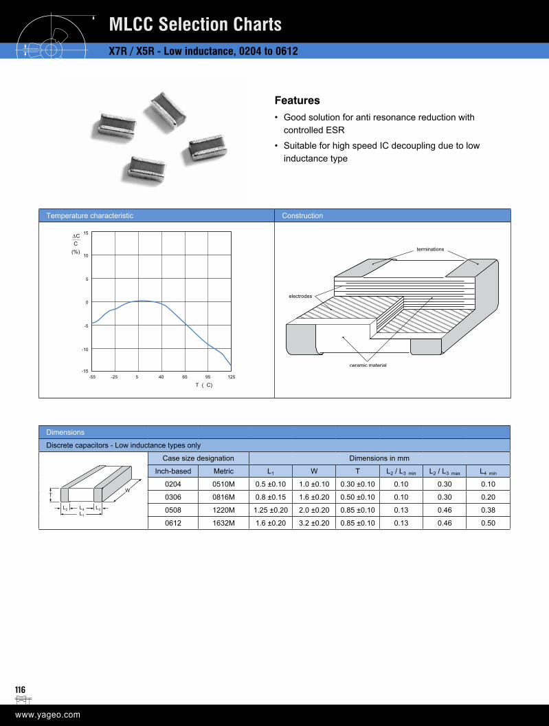
116
X7R / X5R - Low inductance, 0204 to 0612
MLCC Selection Charts
Temperature characteristic Construction
Dimensions
Discrete capacitors - Low inductance types only
T
L2 L3L4L1
W
Case size designation Dimensions in mm
Inch-based Metric L1 W T L2 / L3 min L2 / L3 max L4 min
0204 0510M 0.5 ±0.10 1.0 ±0.10 0.30 ±0.10 0.10 0.30 0.10
0306 0816M 0.8 ±0.15 1.6 ±0.20 0.50 ±0.10 0.10 0.30 0.20
0508 1220M 1.25 ±0.20 2.0 ±0.20 0.85 ±0.10 0.13 0.46 0.38
0612 1632M 1.6 ±0.20 3.2 ±0.20 0.85 ±0.10 0.13 0.46 0.50
Features• Good solution for anti resonance reduction with
controlled ESR
• Suitable for high speed IC decoupling due to low inductance type
15
5
-15-25-55 5 40 9565 125
10
-10
∆CC
(%)
-5
0
T ( C)
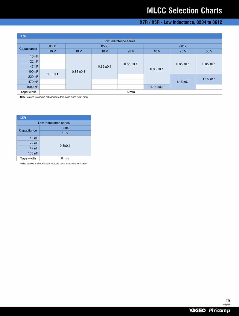
117
X7R / X5R - Low inductance, 0204 to 0612
MLCC Selection Charts
X7RLow Inductance series
Capacitance0306 0508 061210 V 10 V 16 V 25 V 16 V 25 V 50 V
10 nF
0.85 ±0.10.85 ±0.1
0.85 ±0.10.85 ±0.1
0.85 ±0.1 0.85 ±0.122 nF47 nF
100 nF0.5 ±0.1
220 nF1.15 ±0.1
1.15 ±0.1470 nF
1000 nF 1.15 ±0.1Tape width 8 mmNote: Values in shaded cells indicate thickness class (unit: mm)
X5RLow Inductance series
Capacitance020410 V
10 nF
0.3±0.122 nF47 nF
100 nFTape width 8 mmNote: Values in shaded cells indicate thickness class (unit: mm)
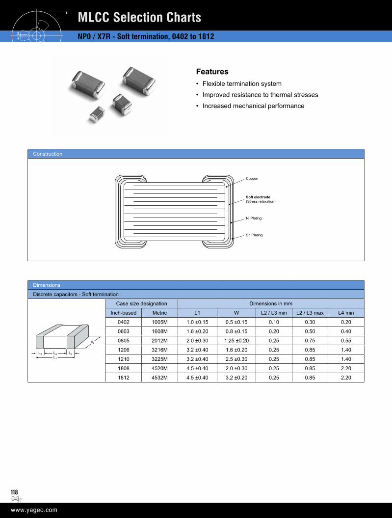
118
NP0 / X7R - Soft termination, 0402 to 1812
MLCC Selection Charts
Construction
Dimensions
Discrete capacitors - Soft termination
Case size designation Dimensions in mm
Inch-based Metric L1 W L2 / L3 min L2 / L3 max L4 min
0402 1005M 1.0 ±0.15 0.5 ±0.15 0.10 0.30 0.20
0603 1608M 1.6 ±0.20 0.8 ±0.15 0.20 0.50 0.40
0805 2012M 2.0 ±0.30 1.25 ±0.20 0.25 0.75 0.55
1206 3216M 3.2 ±0.40 1.6 ±0.20 0.25 0.85 1.40
1210 3225M 3.2 ±0.40 2.5 ±0.30 0.25 0.85 1.40
1808 4520M 4.5 ±0.40 2.0 ±0.30 0.25 0.85 2.20
1812 4532M 4.5 ±0.40 3.2 ±0.20 0.25 0.85 2.20
Features• Flexible termination system
• Improved resistance to thermal stresses
• Increased mechanical performance
Copper
Ni Plating
Sn Plating
Soft electrode(Stress relaxation)
L2 L3L4L1
W
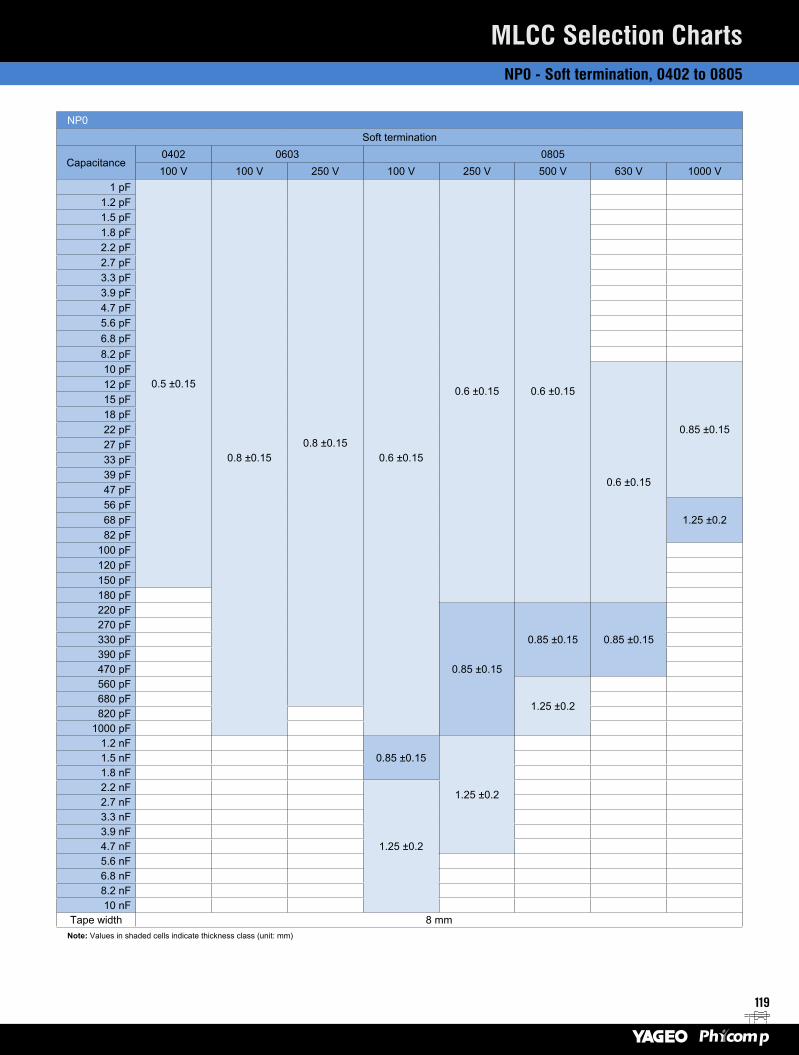
119
NP0 - Soft termination, 0402 to 0805
MLCC Selection Charts
NP0Soft termination
Capacitance0402 0603 0805100 V 100 V 250 V 100 V 250 V 500 V 630 V 1000 V
1 pF
0.5 ±0.15
0.8 ±0.150.8 ±0.15
0.6 ±0.15
0.6 ±0.15 0.6 ±0.15
1.2 pF1.5 pF1.8 pF2.2 pF2.7 pF3.3 pF3.9 pF4.7 pF5.6 pF6.8 pF8.2 pF10 pF
0.6 ±0.15
0.85 ±0.15
12 pF15 pF18 pF22 pF27 pF33 pF39 pF47 pF56 pF
1.25 ±0.268 pF82 pF
100 pF120 pF150 pF180 pF220 pF
0.85 ±0.15
0.85 ±0.15 0.85 ±0.15270 pF330 pF390 pF470 pF560 pF
1.25 ±0.2680 pF820 pF
1000 pF1.2 nF
0.85 ±0.15
1.25 ±0.2
1.5 nF1.8 nF2.2 nF
1.25 ±0.2
2.7 nF3.3 nF3.9 nF4.7 nF5.6 nF6.8 nF8.2 nF10 nF
Tape width 8 mmNote: Values in shaded cells indicate thickness class (unit: mm)
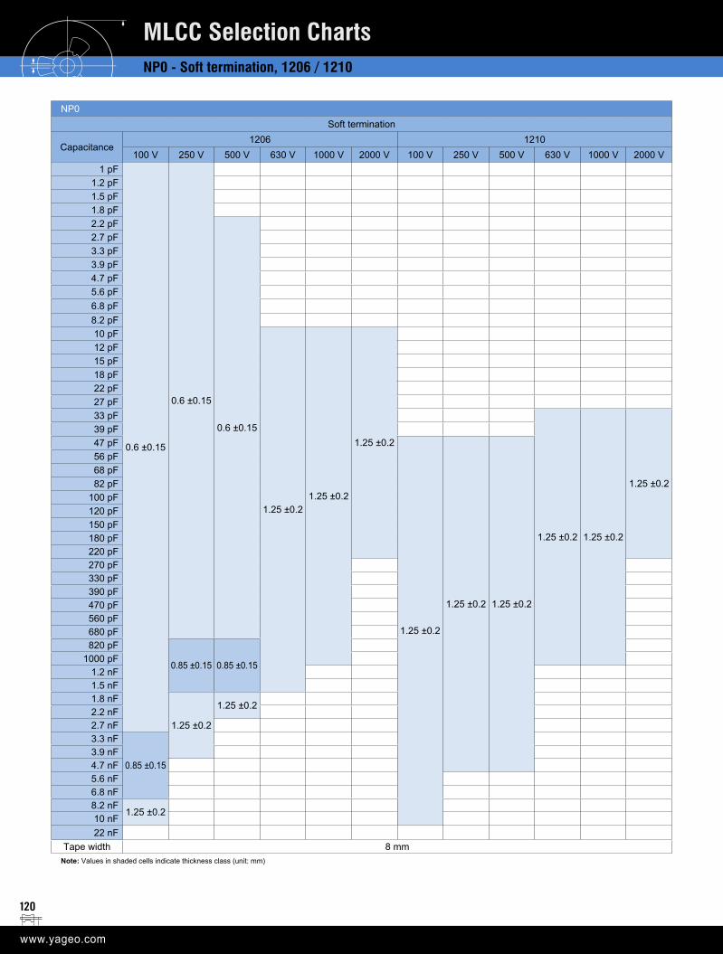
120
NP0 - Soft termination, 1206 / 1210
MLCC Selection Charts
NP0Soft termination
Capacitance1206 1210
100 V 250 V 500 V 630 V 1000 V 2000 V 100 V 250 V 500 V 630 V 1000 V 2000 V1 pF
0.6 ±0.15
0.6 ±0.15
1.2 pF1.5 pF1.8 pF2.2 pF
0.6 ±0.15
2.7 pF3.3 pF3.9 pF4.7 pF5.6 pF6.8 pF8.2 pF10 pF
1.25 ±0.21.25 ±0.2
1.25 ±0.2
12 pF15 pF18 pF22 pF27 pF33 pF
1.25 ±0.2 1.25 ±0.2
1.25 ±0.2
39 pF47 pF
1.25 ±0.2
1.25 ±0.2 1.25 ±0.2
56 pF68 pF82 pF
100 pF120 pF150 pF180 pF220 pF270 pF330 pF390 pF470 pF560 pF680 pF820 pF
0.85 ±0.15 0.85 ±0.151000 pF
1.2 nF1.5 nF1.8 nF
1.25 ±0.2
1.25 ±0.22.2 nF2.7 nF3.3 nF
0.85 ±0.153.9 nF4.7 nF5.6 nF6.8 nF8.2 nF
1.25 ±0.210 nF22 nF
Tape width 8 mmNote: Values in shaded cells indicate thickness class (unit: mm)
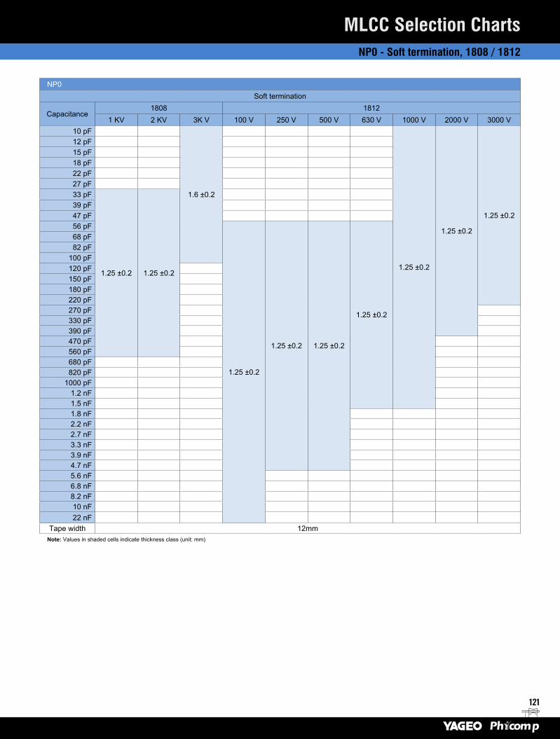
121
NP0 - Soft termination, 1808 / 1812
MLCC Selection Charts
NP0Soft termination
Capacitance1808 1812
1 KV 2 KV 3K V 100 V 250 V 500 V 630 V 1000 V 2000 V 3000 V10 pF
1.6 ±0.2
1.25 ±0.2
1.25 ±0.2
1.25 ±0.2
12 pF15 pF18 pF22 pF27 pF33 pF
1.25 ±0.2 1.25 ±0.2
39 pF47 pF56 pF
1.25 ±0.2
1.25 ±0.2 1.25 ±0.2
1.25 ±0.2
68 pF82 pF
100 pF120 pF150 pF180 pF220 pF270 pF330 pF390 pF470 pF560 pF680 pF820 pF
1000 pF1.2 nF1.5 nF1.8 nF2.2 nF2.7 nF3.3 nF3.9 nF4.7 nF5.6 nF6.8 nF8.2 nF10 nF22 nF
Tape width 12mmNote: Values in shaded cells indicate thickness class (unit: mm)
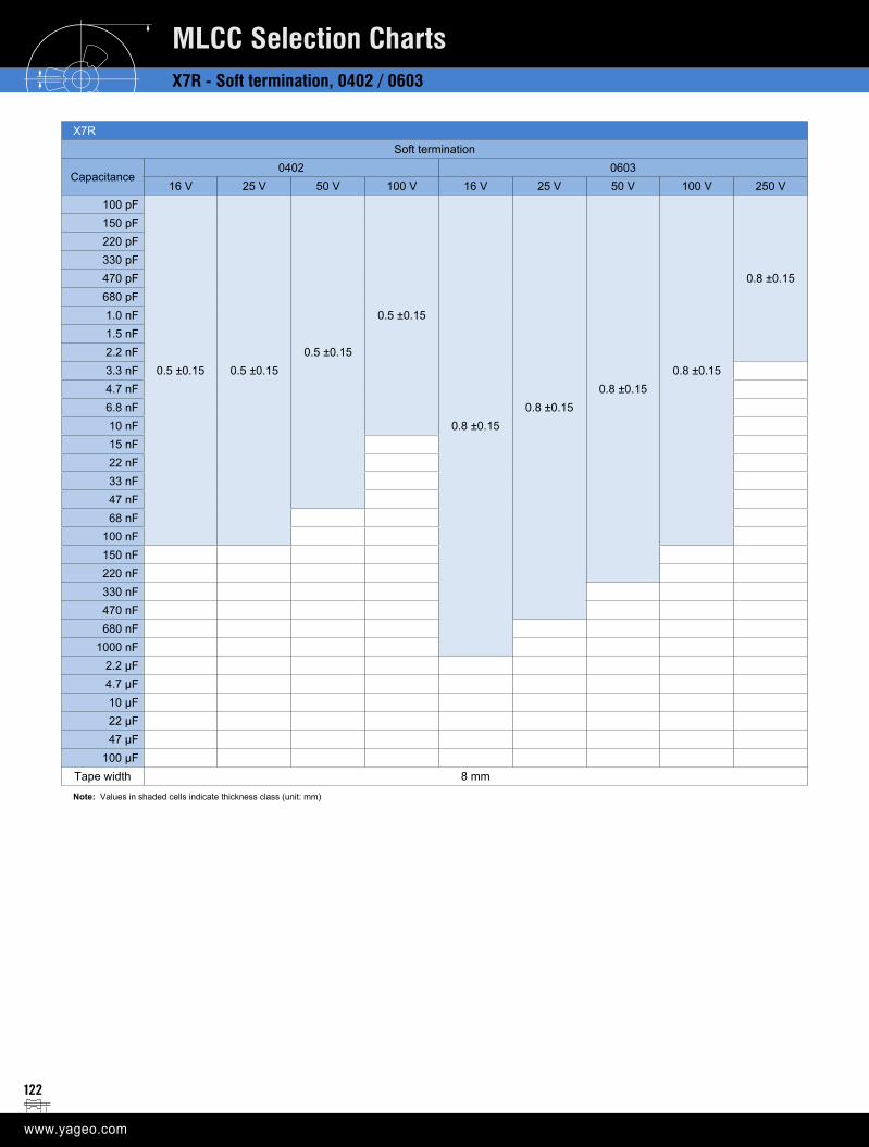
122
X7RSoft termination
Capacitance0402 0603
16 V 25 V 50 V 100 V 16 V 25 V 50 V 100 V 250 V100 pF
0.5 ±0.15 0.5 ±0.150.5 ±0.15
0.5 ±0.15
0.8 ±0.150.8 ±0.15
0.8 ±0.150.8 ±0.15
0.8 ±0.15
150 pF220 pF330 pF470 pF680 pF1.0 nF1.5 nF2.2 nF3.3 nF4.7 nF6.8 nF10 nF15 nF22 nF33 nF47 nF68 nF
100 nF150 nF220 nF330 nF470 nF680 nF
1000 nF2.2 µF4.7 µF10 µF22 µF47 µF
100 µFTape width 8 mm
Note: Values in shaded cells indicate thickness class (unit: mm)
X7R - Soft termination, 0402 / 0603
MLCC Selection Charts
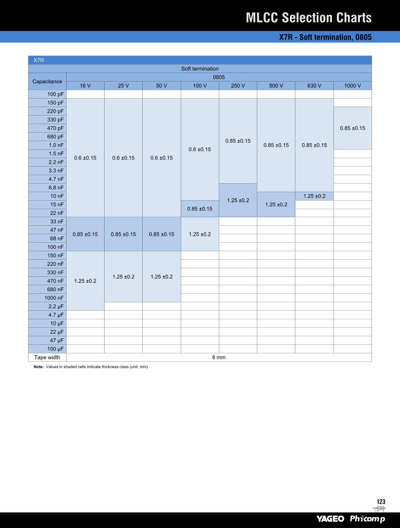
123
X7R - Soft termination, 0805
MLCC Selection Charts
X7RSoft termination
Capacitance0805
16 V 25 V 50 V 100 V 250 V 500 V 630 V 1000 V100 pF150 pF
0.6 ±0.15 0.6 ±0.15 0.6 ±0.150.6 ±0.15
0.85 ±0.150.85 ±0.15 0.85 ±0.15
220 pF
0.85 ±0.15330 pF470 pF680 pF1.0 nF1.5 nF2.2 nF3.3 nF4.7 nF6.8 nF
1.25 ±0.210 nF
1.25 ±0.21.25 ±0.2
15 nF0.85 ±0.15
22 nF33 nF
0.85 ±0.15 0.85 ±0.15 0.85 ±0.15 1.25 ±0.247 nF68 nF
100 nF150 nF
1.25 ±0.21.25 ±0.2 1.25 ±0.2
220 nF330 nF470 nF680 nF
1000 nF2.2 µF4.7 µF10 µF22 µF47 µF
100 µFTape width 8 mm
Note: Values in shaded cells indicate thickness class (unit: mm)
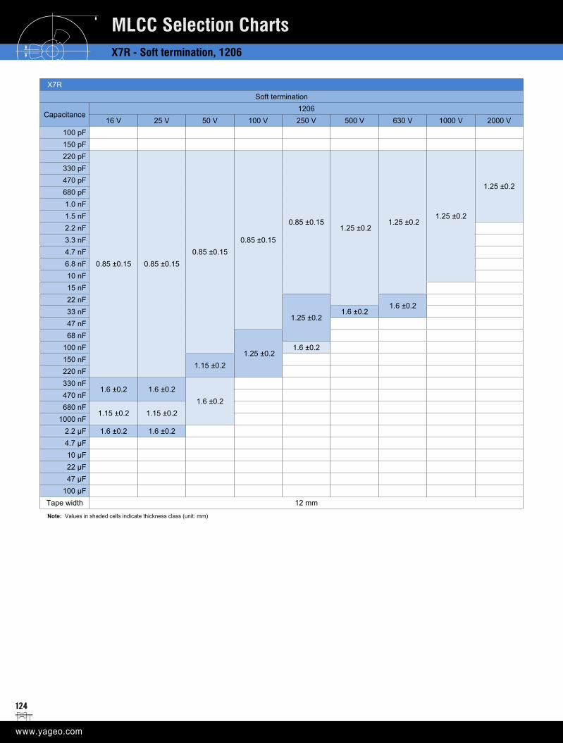
124
X7R - Soft termination, 1206
MLCC Selection Charts
X7RSoft termination
Capacitance1206
16 V 25 V 50 V 100 V 250 V 500 V 630 V 1000 V 2000 V100 pF150 pF220 pF
0.85 ±0.15 0.85 ±0.150.85 ±0.15
0.85 ±0.15
0.85 ±0.15 1.25 ±0.2
1.25 ±0.21.25 ±0.2
1.25 ±0.2
330 pF470 pF680 pF1.0 nF1.5 nF2.2 nF3.3 nF4.7 nF6.8 nF10 nF15 nF22 nF
1.25 ±0.21.6 ±0.2
33 nF 1.6 ±0.247 nF68 nF
1.25 ±0.2100 nF 1.6 ±0.2150 nF
1.15 ±0.2220 nF330 nF
1.6 ±0.2 1.6 ±0.21.6 ±0.2
470 nF680 nF
1.15 ±0.2 1.15 ±0.21000 nF
2.2 µF 1.6 ±0.2 1.6 ±0.24.7 µF10 µF22 µF47 µF
100 µFTape width 12 mm
Note: Values in shaded cells indicate thickness class (unit: mm)
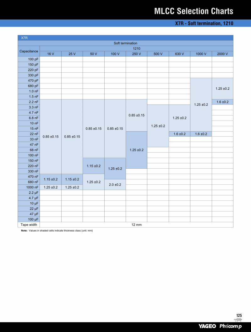
125
X7R - Soft termination, 1210
MLCC Selection Charts
X7RSoft termination
Capacitance1210
16 V 25 V 50 V 100 V 250 V 500 V 630 V 1000 V 2000 V100 pF150 pF220 pF330 pF470 pF
1.25 ±0.2
1.25 ±0.2680 pF1.0 nF1.5 nF2.2 nF
0.85 ±0.15 0.85 ±0.15
0.85 ±0.15 0.85 ±0.15
0.85 ±0.15
1.6 ±0.23.3 nF
1.25 ±0.2
1.25 ±0.24.7 nF6.8 nF10 nF15 nF22 nF
1.25 ±0.2
1.6 ±0.2 1.6 ±0.233 nF47 nF68 nF
100 nF150 nF
1.15 ±0.21.25 ±0.2
220 nF330 nF470 nF
1.15 ±0.2 1.15 ±0.21.25 ±0.2680 nF
2.0 ±0.21000 nF 1.25 ±0.2 1.25 ±0.2
2.2 µF4.7 µF10 µF22 µF47 µF
100 µFTape width 12 mm
Note: Values in shaded cells indicate thickness class (unit: mm)
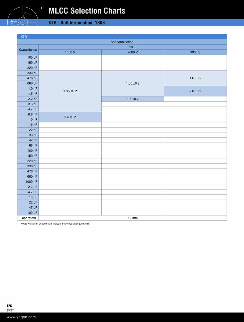
126
MLCC Selection Charts
X7RSoft termination
Capacitance1808
1000 V 2000 V 3000 V100 pF150 pF220 pF330 pF
1.35 ±0.2
1.35 ±0.21.6 ±0.2470 pF
680 pF1.0 nF
2.0 ±0.21.5 nF2.2 nF 1.6 ±0.23.3 nF4.7 nF6.8 nF
1.6 ±0.210 nF15 nF22 nF33 nF47 nF68 nF
100 nF150 nF220 nF330 nF470 nF680 nF
1000 nF2.2 µF4.7 µF10 µF22 µF47 µF
100 µFTape width 12 mm
Note: Values in shaded cells indicate thickness class (unit: mm)
X7R - Soft termination, 1808
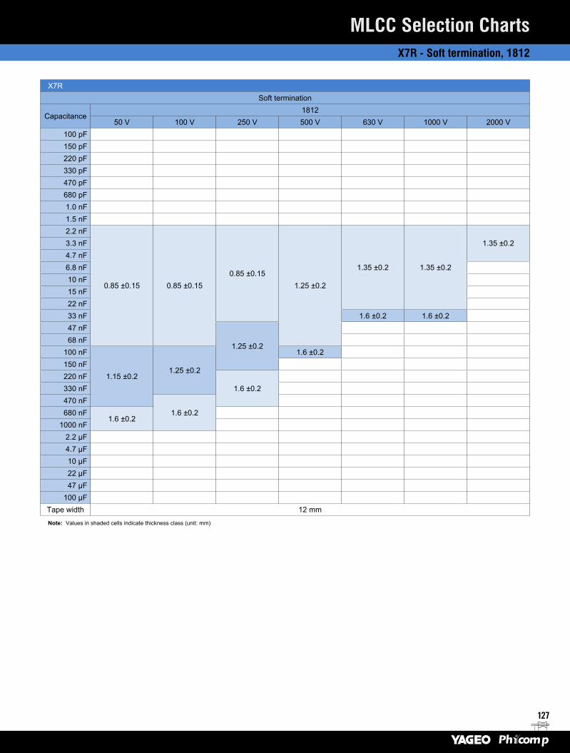
127
MLCC Selection Charts
X7RSoft termination
Capacitance1812
50 V 100 V 250 V 500 V 630 V 1000 V 2000 V100 pF150 pF220 pF330 pF470 pF680 pF1.0 nF1.5 nF2.2 nF
0.85 ±0.15 0.85 ±0.150.85 ±0.15
1.25 ±0.2
1.35 ±0.2 1.35 ±0.2
1.35 ±0.23.3 nF4.7 nF6.8 nF10 nF15 nF22 nF33 nF 1.6 ±0.2 1.6 ±0.247 nF
1.25 ±0.268 nF
100 nF
1.15 ±0.21.25 ±0.2
1.6 ±0.2150 nF220 nF
1.6 ±0.2330 nF470 nF
1.6 ±0.2680 nF1.6 ±0.2
1000 nF2.2 µF4.7 µF10 µF22 µF47 µF
100 µFTape width 12 mm
Note: Values in shaded cells indicate thickness class (unit: mm)
X7R - Soft termination, 1812
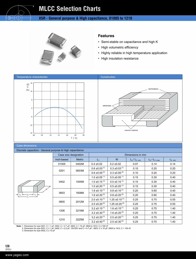
128
X5R - General purpose & High capacitance, 01005 to 1210
MLCC Selection Charts
Temperature characteristic Construction
Case dimensions
Discrete capacitors - General purpose & High capacitance
L2 L3L4L1
W
Case size designation Dimensions in mm
Inch-based Metric L1 W L2 / L3 min L2 / L3 max L4 min
01005 0402M 0.4 ±0.02 0.2 ±0.02 0.07 0.14 0.14
0201 0603M0.6 ±0.03 (1) 0.3 ±0.03 (1) 0.10 0.20 0.20
0.6 ±0.05 (2) 0.3 ±0.05 (2) 0.10 0.20 0.20
0402 1005M
1.0 ±0.05 (1) 0.5 ±0.05 (1) 0.15 0.30 0.40
1.0 ±0.15 (2) 0.5 ±0.15 (2) 0.15 0.30 0.40
1.0 ±0.20 (3) 0.5 ±0.20 (3) 0.15 0.30 0.40
0603 1608M1.6 ±0.10 (1) 0.8 ±0.10 (1) 0.20 0.60 0.40
1.6 ±0.20 (2) 0.8 ±0.20 (2) 0.20 0.60 0.40
0805 2012M2.0 ±0.10 (1) 1.25 ±0.10 (1) 0.25 0.75 0.55
2.0 ±0.20 (2) 1.25 ±0.20 (2) 0.25 0.75 0.55
1206 3216M3.2 ±0.15 (1) 1.6 ±0.15 (1) 0.25 0.75 1.40
3.2 ±0.30 (2) 1.6 ±0.20 (2) 0.25 0.75 1.40
1210 3225M3.2 ±0.20 (1) 2.5 ±0.20 (1) 0.25 0.75 1.40
3.2 ±0.40 (2) 2.5 ±0.30 (2) 0.25 0.75 1.40Note: 1. Dimension for size 0201, C < 1 μF; 0402, C < 4.7 μF; 0603, C < 10 μF; 0805 to 1812, C ≤ 100 nF 2. Dimension for size 0201, C ≥ 1 μF; 0402, C = 2.2 μF, 16V/25V and C = 4.7 μF ; 0603, C ≥ 10 μF; 0805 to 1812, C > 100 nF 3. Dimension for size 0402, C ≥ 10 μF
Features• Semi-stable on capacitance and high K
• High volumetric efficiency
• Highly reliable in high temperature application
• High insulation resistance
15
5
-15-35-60 -10 15 6540 90
10
-10
C(%)
-5
0
T ( C)
∆C
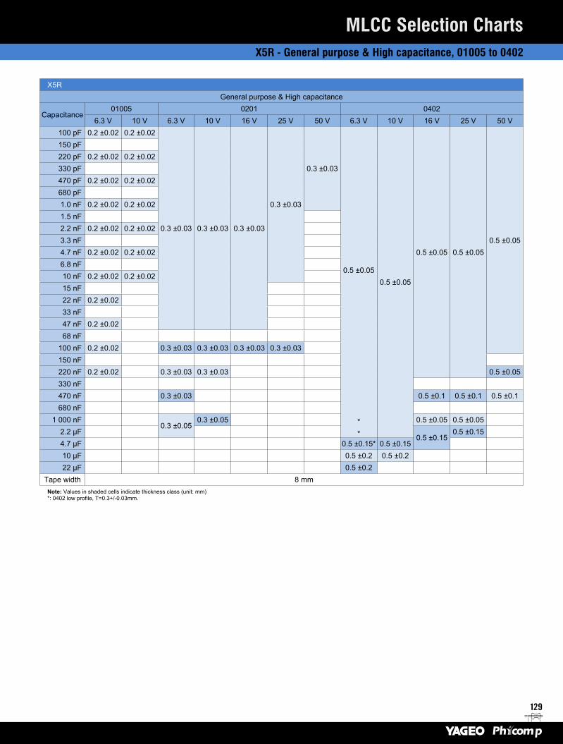
129
Temperature characteristic Construction
Case dimensions
Discrete capacitors - General purpose & High capacitance
L2 L3L4L1
W
Case size designation Dimensions in mm
Inch-based Metric L1 W L2 / L3 min L2 / L3 max L4 min
01005 0402M 0.4 ±0.02 0.2 ±0.02 0.07 0.14 0.14
0201 0603M0.6 ±0.03 (1) 0.3 ±0.03 (1) 0.10 0.20 0.20
0.6 ±0.05 (2) 0.3 ±0.05 (2) 0.10 0.20 0.20
0402 1005M
1.0 ±0.05 (1) 0.5 ±0.05 (1) 0.15 0.30 0.40
1.0 ±0.15 (2) 0.5 ±0.15 (2) 0.15 0.30 0.40
1.0 ±0.20 (3) 0.5 ±0.20 (3) 0.15 0.30 0.40
0603 1608M1.6 ±0.10 (1) 0.8 ±0.10 (1) 0.20 0.60 0.40
1.6 ±0.20 (2) 0.8 ±0.20 (2) 0.20 0.60 0.40
0805 2012M2.0 ±0.10 (1) 1.25 ±0.10 (1) 0.25 0.75 0.55
2.0 ±0.20 (2) 1.25 ±0.20 (2) 0.25 0.75 0.55
1206 3216M3.2 ±0.15 (1) 1.6 ±0.15 (1) 0.25 0.75 1.40
3.2 ±0.30 (2) 1.6 ±0.20 (2) 0.25 0.75 1.40
1210 3225M3.2 ±0.20 (1) 2.5 ±0.20 (1) 0.25 0.75 1.40
3.2 ±0.40 (2) 2.5 ±0.30 (2) 0.25 0.75 1.40Note: 1. Dimension for size 0201, C < 1 μF; 0402, C < 4.7 μF; 0603, C < 10 μF; 0805 to 1812, C ≤ 100 nF 2. Dimension for size 0201, C ≥ 1 μF; 0402, C = 2.2 μF, 16V/25V and C = 4.7 μF ; 0603, C ≥ 10 μF; 0805 to 1812, C > 100 nF 3. Dimension for size 0402, C ≥ 10 μF
X5R - General purpose & High capacitance, 01005 to 0402
MLCC Selection Charts
X5RGeneral purpose & High capacitance
Capacitance01005 0201 0402
6.3 V 10 V 6.3 V 10 V 16 V 25 V 50 V 6.3 V 10 V 16 V 25 V 50 V100 pF 0.2 ±0.02 0.2 ±0.02
0.3 ±0.03 0.3 ±0.03 0.3 ±0.03
0.3 ±0.03
0.3 ±0.03
0.5 ±0.050.5 ±0.05
0.5 ±0.05 0.5 ±0.050.5 ±0.05
150 pF220 pF 0.2 ±0.02 0.2 ±0.02330 pF470 pF 0.2 ±0.02 0.2 ±0.02680 pF1.0 nF 0.2 ±0.02 0.2 ±0.021.5 nF2.2 nF 0.2 ±0.02 0.2 ±0.023.3 nF4.7 nF 0.2 ±0.02 0.2 ±0.026.8 nF10 nF 0.2 ±0.02 0.2 ±0.0215 nF22 nF 0.2 ±0.0233 nF47 nF 0.2 ±0.0268 nF
100 nF 0.2 ±0.02 0.3 ±0.03 0.3 ±0.03 0.3 ±0.03 0.3 ±0.03150 nF220 nF 0.2 ±0.02 0.3 ±0.03 0.3 ±0.03 0.5 ±0.05330 nF470 nF 0.3 ±0.03 0.5 ±0.1 0.5 ±0.1 0.5 ±0.1680 nF
1 000 nF0.3 ±0.05
0.3 ±0.05 * 0.5 ±0.05 0.5 ±0.052.2 µF * 0.5 ±0.15
0.5 ±0.15 4.7 µF 0.5 ±0.15* 0.5 ±0.1510 μF 0.5 ±0.2 0.5 ±0.222 μF 0.5 ±0.2
Tape width 8 mmNote: Values in shaded cells indicate thickness class (unit: mm)*: 0402 low profile, T=0.3+/-0.03mm.
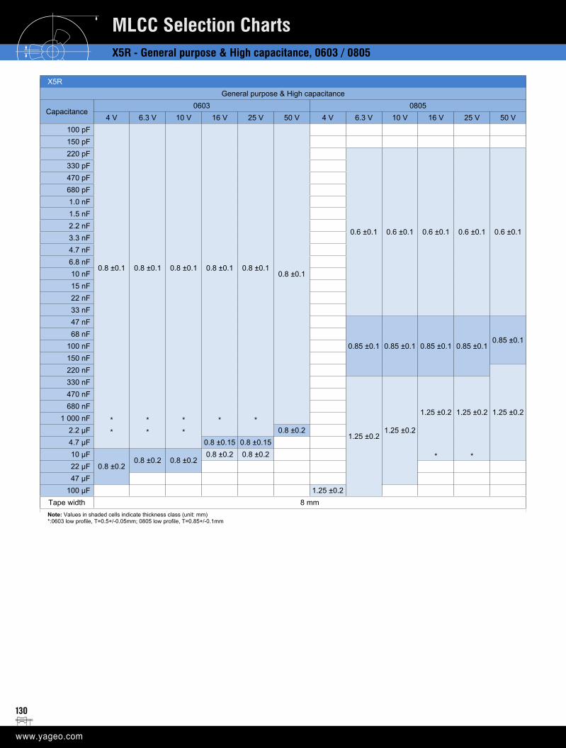
130
X5R - General purpose & High capacitance, 0603 / 0805
MLCC Selection Charts
X5RGeneral purpose & High capacitance
Capacitance0603 0805
4 V 6.3 V 10 V 16 V 25 V 50 V 4 V 6.3 V 10 V 16 V 25 V 50 V100 pF
0.8 ±0.1 0.8 ±0.1 0.8 ±0.1 0.8 ±0.1 0.8 ±0.10.8 ±0.1
150 pF220 pF
0.6 ±0.1 0.6 ±0.1 0.6 ±0.1 0.6 ±0.1 0.6 ±0.1
330 pF470 pF680 pF1.0 nF1.5 nF2.2 nF3.3 nF4.7 nF6.8 nF10 nF15 nF22 nF33 nF47 nF
0.85 ±0.1 0.85 ±0.1 0.85 ±0.1 0.85 ±0.10.85 ±0.1
68 nF100 nF150 nF220 nF
1.25 ±0.2
330 nF
1.25 ±0.2 1.25 ±0.21.25 ±0.2 1.25 ±0.2
470 nF680 nF
1 000 nF * * * * *2.2 µF * * * 0.8 ±0.24.7 µF 0.8 ±0.15 0.8 ±0.15 * *10 µF
0.8 ±0.20.8 ±0.2 0.8 ±0.2
0.8 ±0.2 0.8 ±0.2 * * * *22 µF * *47 µF
100 µF 1.25 ±0.2 1.25 ±0.2Tape width 8 mmNote: Values in shaded cells indicate thickness class (unit: mm)*:0603 low profile, T=0.5+/-0.05mm; 0805 low profile, T=0.85+/-0.1mm
X5RGeneral purpose & High capacitance
Capacitance0603 0805
4 V 6.3 V 10 V 16 V 25 V 50 V 4 V 6.3 V 10 V 16 V 25 V 50 V100 pF
0.8 ±0.1 0.8 ±0.1 0.8 ±0.1 0.8 ±0.1 0.8 ±0.10.8 ±0.1
150 pF220 pF
0.6 ±0.1 0.6 ±0.1 0.6 ±0.1 0.6 ±0.1 0.6 ±0.1
330 pF470 pF680 pF1.0 nF1.5 nF2.2 nF3.3 nF4.7 nF6.8 nF10 nF15 nF22 nF33 nF47 nF
0.85 ±0.1 0.85 ±0.1 0.85 ±0.1 0.85 ±0.10.85 ±0.1
68 nF100 nF150 nF220 nF
1.25 ±0.2
330 nF
1.25 ±0.21.25 ±0.2
1.25 ±0.2 1.25 ±0.2
470 nF680 nF
1 000 nF * * * * *2.2 µF * * * 0.8 ±0.24.7 µF 0.8 ±0.15 0.8 ±0.1510 µF
0.8 ±0.20.8 ±0.2 0.8 ±0.2
0.8 ±0.2 0.8 ±0.2 * *22 µF47 µF
100 µF 1.25 ±0.2Tape width 8 mmNote: Values in shaded cells indicate thickness class (unit: mm)*:0603 low profile, T=0.5+/-0.05mm; 0805 low profile, T=0.85+/-0.1mm
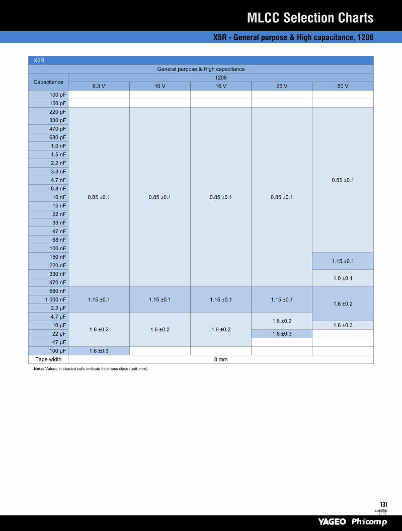
131
X5R - General purpose & High capacitance, 1206
MLCC Selection Charts
X5RGeneral purpose & High capacitance
Capacitance1206
6.3 V 10 V 16 V 25 V 50 V100 pF150 pF220 pF
0.85 ±0.1 0.85 ±0.1 0.85 ±0.1 0.85 ±0.1
0.85 ±0.1
330 pF470 pF680 pF1.0 nF1.5 nF2.2 nF3.3 nF4.7 nF6.8 nF10 nF15 nF22 nF33 nF47 nF68 nF
100 nF150 nF
1.15 ±0.1220 nF330 nF
1.0 ±0.1470 nF680 nF
1.15 ±0.1 1.15 ±0.1 1.15 ±0.1 1.15 ±0.11.6 ±0.2
1 000 nF2.2 µF4.7 µF
1.6 ±0.2 1.6 ±0.2 1.6 ±0.21.6 ±0.2
10 µF 1.6 ±0.322 µF 1.6 ±0.347 µF
100 µF 1.6 ±0.3Tape width 8 mm
Note: Values in shaded cells indicate thickness class (unit: mm)
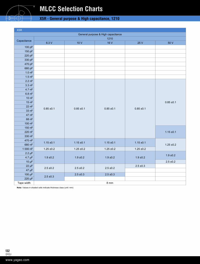
132
X5R - General purpose & High capacitance, 1210
MLCC Selection Charts
X5RGeneral purpose & High capacitance
Capacitance1210
6.3 V 10 V 16 V 25 V 50 V100 pF150 pF220 pF330 pF470 pF680 pF1.0 nF1.5 nF2.2 nF
0.85 ±0.1 0.85 ±0.1 0.85 ±0.1 0.85 ±0.1
0.85 ±0.1
3.3 nF4.7 nF6.8 nF10 nF15 nF22 nF33 nF47 nF68 nF
100 nF150 nF
1.15 ±0.1220 nF330 nF470 nF
1.15 ±0.1 1.15 ±0.1 1.15 ±0.1 1.15 ±0.11.25 ±0.2680 nF
1 000 nF 1.25 ±0.2 1.25 ±0.2 1.25 ±0.2 1.25 ±0.22.2 µF
1.9 ±0.2 1.9 ±0.2 1.9 ±0.2 1.9 ±0.21.9 ±0.2
4.7 µF10 µF 2.5 ±0.222 µF
2.5 ±0.2 2.5 ±0.2 2.5 ±0.22.5 ±0.3
47 µF100 µF
2.5 ±0.32.5 ±0.3 2.5 ±0.3
220 µFTape width 8 mm
Note: Values in shaded cells indicate thickness class (unit: mm)
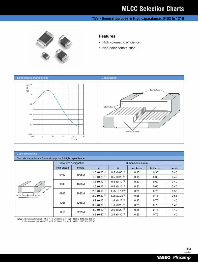
133
Y5V - General purpose & High capacitance, 0402 to 1210
MLCC Selection Charts
Temperature characteristic Construction
Case dimensions
Discrete capacitors - General purpose & High capacitance
L2 L3L4L1
W
Case size designation Dimensions in mm
Inch-based Metric L1 W L2 / L3 min L2 / L3 max L4 min
0402 1005M 1.0 ±0.05 (1) 0.5 ±0.05 (1) 0.15 0.30 0.40
1.0 ±0.20 (2) 0.5 ±0.20 (2) 0.15 0.30 0.40
0603 1608M 1.6 ±0.10 (1) 0.8 ±0.10 (1) 0.20 0.60 0.40
1.6 ±0.15 (2) 0.8 ±0.15 (2) 0.20 0.60 0.40
0805 2012M 2.0 ±0.10 (1) 1.25 ±0.10 (1) 0.25 0.75 0.55
2.0 ±0.20 (2) 1.25 ±0.20 (2) 0.25 0.75 0.55
1206 3216M 3.2 ±0.15 (1) 1.6 ±0.15 (1) 0.25 0.75 1.40
3.2 ±0.30 (2) 1.6 ±0.20 (2) 0.25 0.75 1.40
1210 3225M 3.2 ±0.20 (1) 2.5 ±0.20 (1) 0.25 0.75 1.40
3.2 ±0.40 (2) 2.5 ±0.30 (2) 0.25 0.75 1.40Note: 1. Dimension for size 0402, C < 4.7 μF; 0603, C < 10 μF; 0805 to 1210, C ≤ 100 nF 2. Dimension for size 0402, C ≥ 4.7 μF; 0603, C ≥ 10 μF; 0805 to 1210, C > 100 nF
Features• High volumetric efficiency
• Non-polar construction
0
-100-5-30 20 55 9570
25
-75
C(%)
-50
-25
T ( C)
∆C
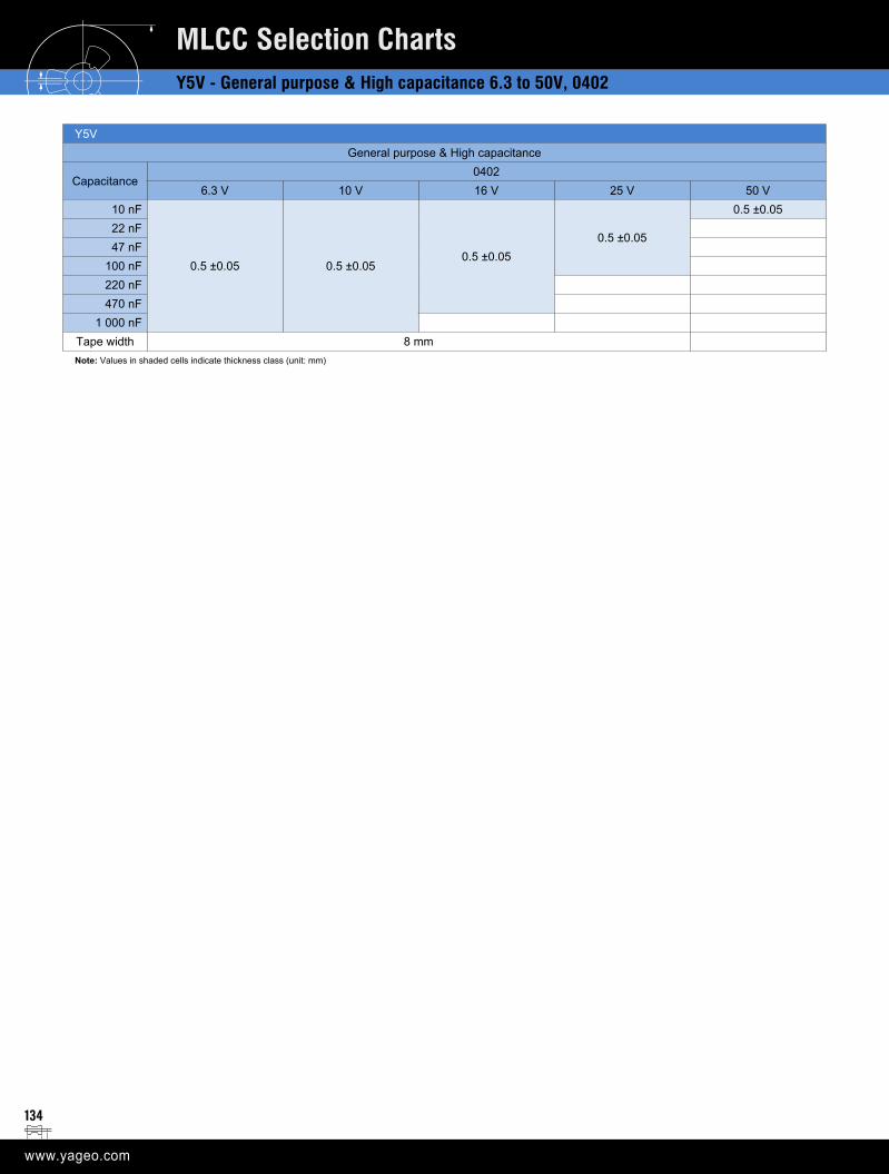
134
Y5V - General purpose & High capacitance 6.3 to 50V, 0402
MLCC Selection Charts
Y5VGeneral purpose & High capacitance
Capacitance0402
6.3 V 10 V 16 V 25 V 50 V10 nF
0.5 ±0.05 0.5 ±0.050.5 ±0.05
0.5 ±0.05
0.5 ±0.0522 nF47 nF
100 nF220 nF470 nF
1 000 nFTape width 8 mmNote: Values in shaded cells indicate thickness class (unit: mm)
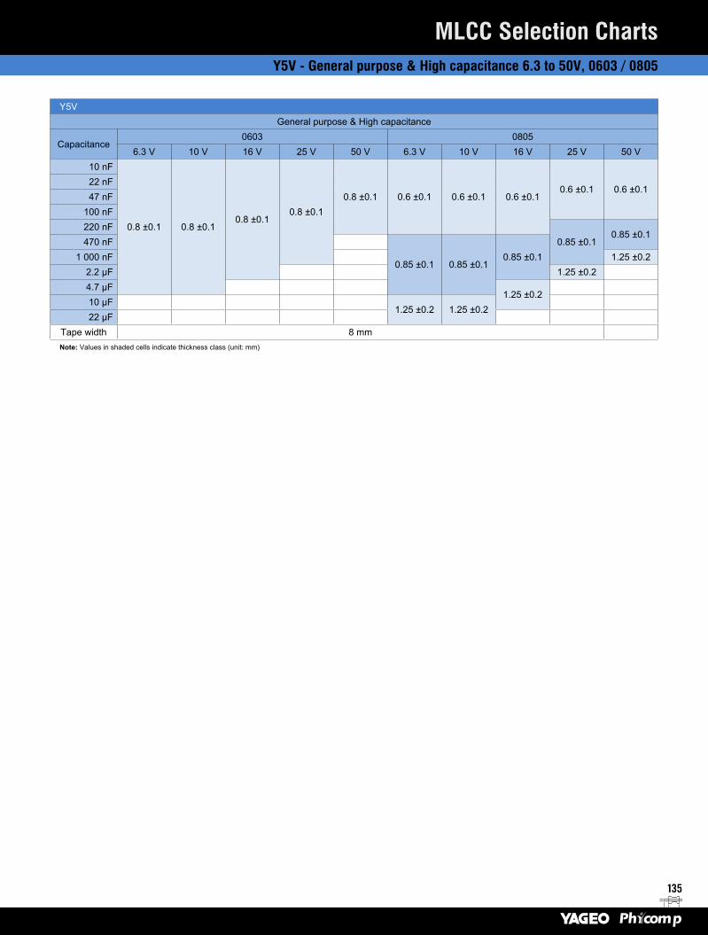
135
Y5V - General purpose & High capacitance 6.3 to 50V, 0603 / 0805
MLCC Selection Charts
Y5VGeneral purpose & High capacitance
Capacitance0603 0805
6.3 V 10 V 16 V 25 V 50 V 6.3 V 10 V 16 V 25 V 50 V10 nF
0.8 ±0.1 0.8 ±0.10.8 ±0.1
0.8 ±0.10.8 ±0.1 0.6 ±0.1 0.6 ±0.1 0.6 ±0.1
0.6 ±0.1 0.6 ±0.122 nF47 nF
100 nF220 nF
0.85 ±0.10.85 ±0.1
470 nF
0.85 ±0.1 0.85 ±0.10.85 ±0.11 000 nF 1.25 ±0.2
2.2 µF 1.25 ±0.24.7 µF
1.25 ±0.210 µF
1.25 ±0.2 1.25 ±0.222 µF
Tape width 8 mmNote: Values in shaded cells indicate thickness class (unit: mm)
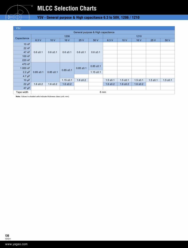
136
Y5V - General purpose & High capacitance 6.3 to 50V, 1206 / 1210
MLCC Selection Charts
Y5VGeneral purpose & High capacitance
Capacitance1206 1210
6.3 V 10 V 16 V 25 V 50 V 6.3 V 10 V 16 V 25 V 50 V10 nF
0.6 ±0.1 0.6 ±0.1 0.6 ±0.1 0.6 ±0.1 0.6 ±0.122 nF47 nF
100 nF220 nF470 nF
0.85 ±0.1 0.85 ±0.10.85 ±0.1
0.85 ±0.10.85 ±0.1
1 000 nF2.2 µF 1.15 ±0.14.7 µF10 µF 1.15 ±0.1 1.6 ±0.2 1.5 ±0.1 1.5 ±0.1 1.5 ±0.1 1.5 ±0.1 1.5 ±0.122 µF 1.6 ±0.2 1.6 ±0.2 1.6 ±0.2 1.6 ±0.2 1.6 ±0.2 1.6 ±0.247 µF
Tape width 8 mm
Note: Values in shaded cells indicate thickness class (unit: mm)
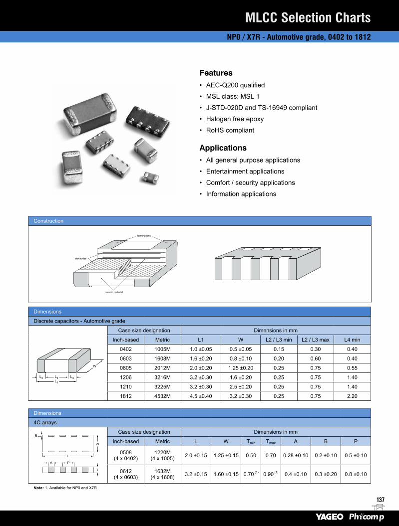
137
NP0 / X7R - Automotive grade, 0402 to 1812
MLCC Selection Charts
Construction
Dimensions
Discrete capacitors - Automotive grade
Case size designation Dimensions in mm
Inch-based Metric L1 W L2 / L3 min L2 / L3 max L4 min
0402 1005M 1.0 ±0.05 0.5 ±0.05 0.15 0.30 0.40
0603 1608M 1.6 ±0.20 0.8 ±0.10 0.20 0.60 0.40
0805 2012M 2.0 ±0.20 1.25 ±0.20 0.25 0.75 0.55
1206 3216M 3.2 ±0.30 1.6 ±0.20 0.25 0.75 1.40
1210 3225M 3.2 ±0.30 2.5 ±0.20 0.25 0.75 1.40
1812 4532M 4.5 ±0.40 3.2 ±0.30 0.25 0.75 2.20
Features• AEC-Q200 qualified
• MSL class: MSL 1
• J-STD-020D and TS-16949 compliant
• Halogen free epoxy
• RoHS compliant
Applications• All general purpose applications
• Entertainment applications
• Comfort / security applications
• Information applications
L2 L3L4L1
W
Dimensions
4C arrays
L
PA
T
B
W
Case size designation Dimensions in mm
Inch-based Metric L W Tmin Tmax A B P
0508 (4 x 0402)
1220M (4 x 1005) 2.0 ±0.15 1.25 ±0.15 0.50 0.70 0.28 ±0.10 0.2 ±0.10 0.5 ±0.10
0612 (4 x 0603)
1632M (4 x 1608) 3.2 ±0.15 1.60 ±0.15 0.70 (1) 0.90 (1) 0.4 ±0.10 0.3 ±0.20 0.8 ±0.10
Note: 1. Available for NP0 and X7R
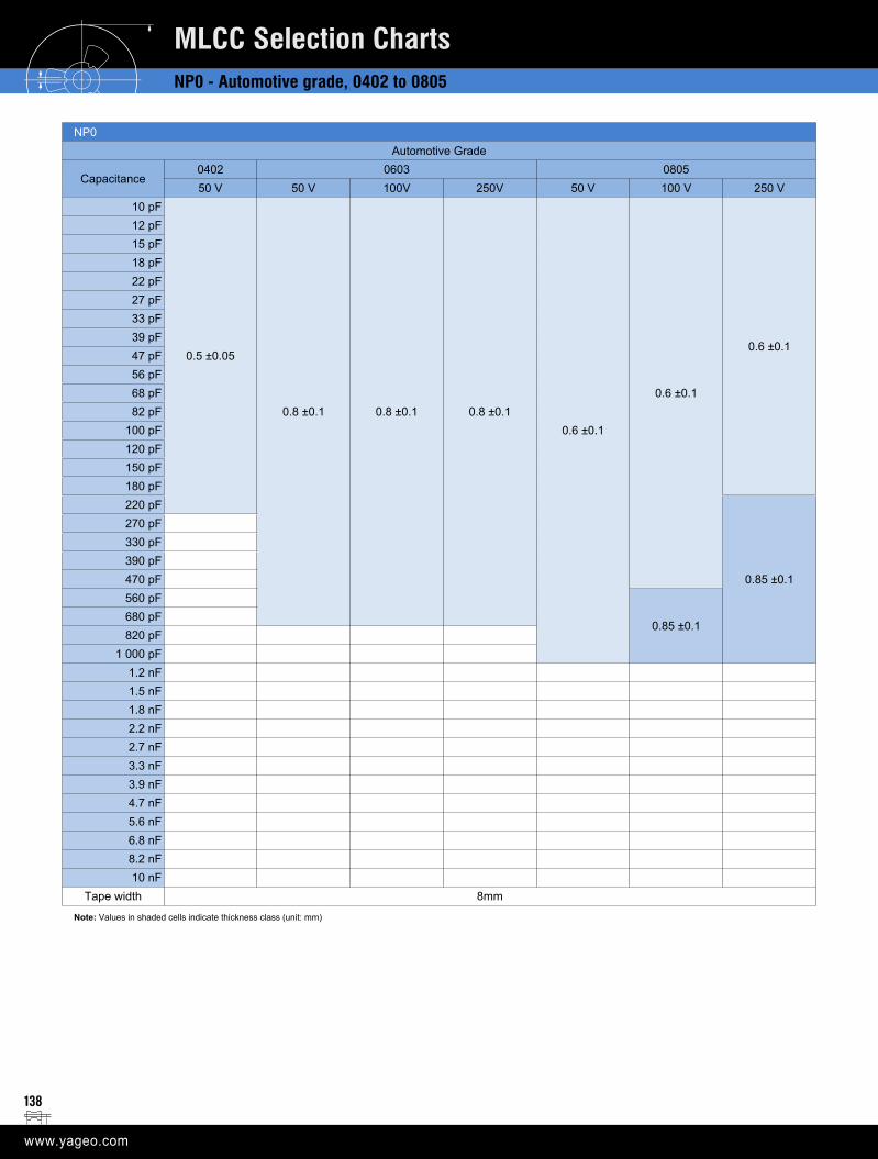
138
NP0 - Automotive grade, 0402 to 0805
MLCC Selection Charts
NP0Automotive Grade
Capacitance0402 0603 080550 V 50 V 100V 250V 50 V 100 V 250 V
10 pF
0.5 ±0.05
0.8 ±0.1 0.8 ±0.1 0.8 ±0.10.6 ±0.1
0.6 ±0.1
0.6 ±0.1
12 pF15 pF18 pF22 pF27 pF33 pF39 pF47 pF56 pF68 pF82 pF
100 pF120 pF150 pF180 pF220 pF
0.85 ±0.1
270 pF330 pF390 pF470 pF560 pF
0.85 ±0.1680 pF820 pF
1 000 pF1.2 nF1.5 nF1.8 nF2.2 nF2.7 nF3.3 nF3.9 nF4.7 nF5.6 nF6.8 nF8.2 nF10 nF
Tape width 8mm
Note: Values in shaded cells indicate thickness class (unit: mm)
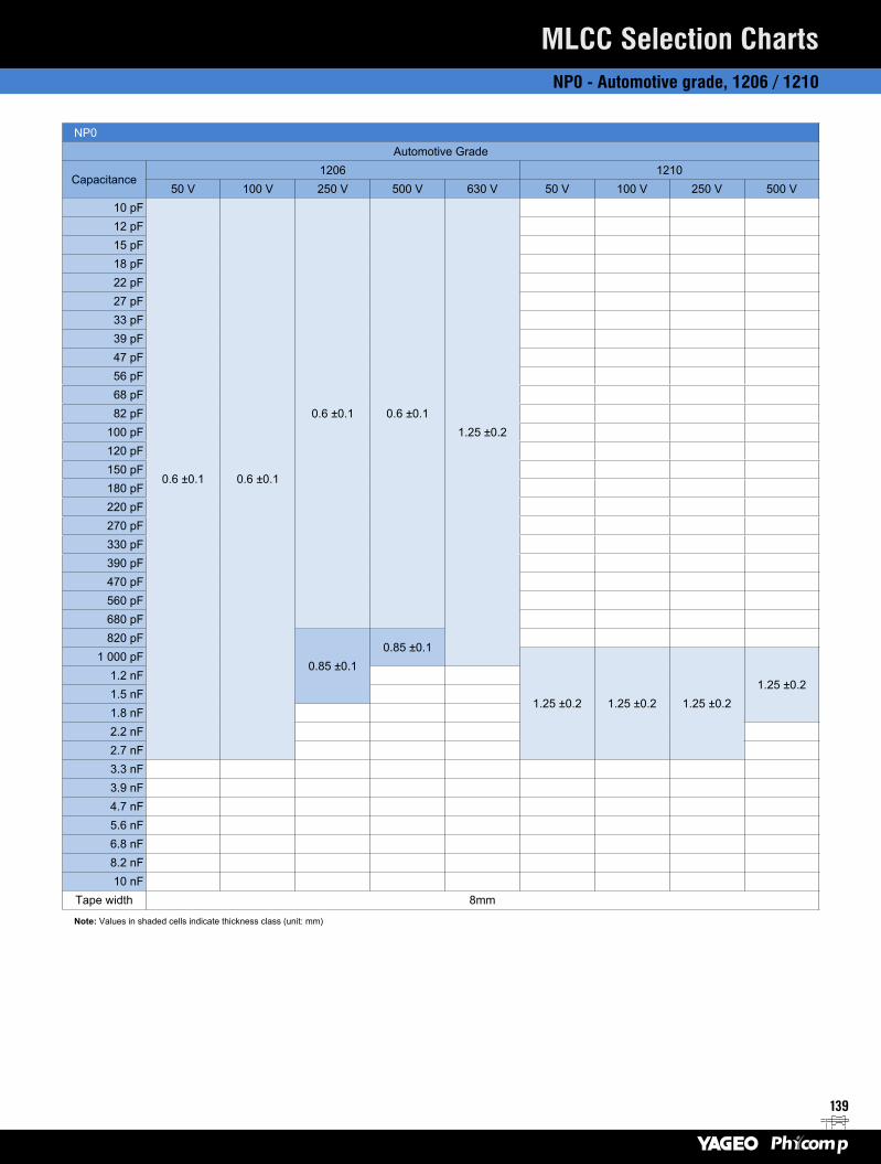
139
NP0 - Automotive grade, 1206 / 1210
MLCC Selection Charts
NP0Automotive Grade
Capacitance1206 1210
50 V 100 V 250 V 500 V 630 V 50 V 100 V 250 V 500 V10 pF
0.6 ±0.1 0.6 ±0.1
0.6 ±0.1 0.6 ±0.11.25 ±0.2
12 pF15 pF18 pF22 pF27 pF33 pF39 pF47 pF56 pF68 pF82 pF
100 pF120 pF150 pF180 pF220 pF270 pF330 pF390 pF470 pF560 pF680 pF820 pF
0.85 ±0.10.85 ±0.1
1 000 pF
1.25 ±0.2 1.25 ±0.2 1.25 ±0.21.25 ±0.2
1.2 nF1.5 nF1.8 nF2.2 nF2.7 nF3.3 nF3.9 nF4.7 nF5.6 nF6.8 nF8.2 nF10 nF
Tape width 8mm
Note: Values in shaded cells indicate thickness class (unit: mm)
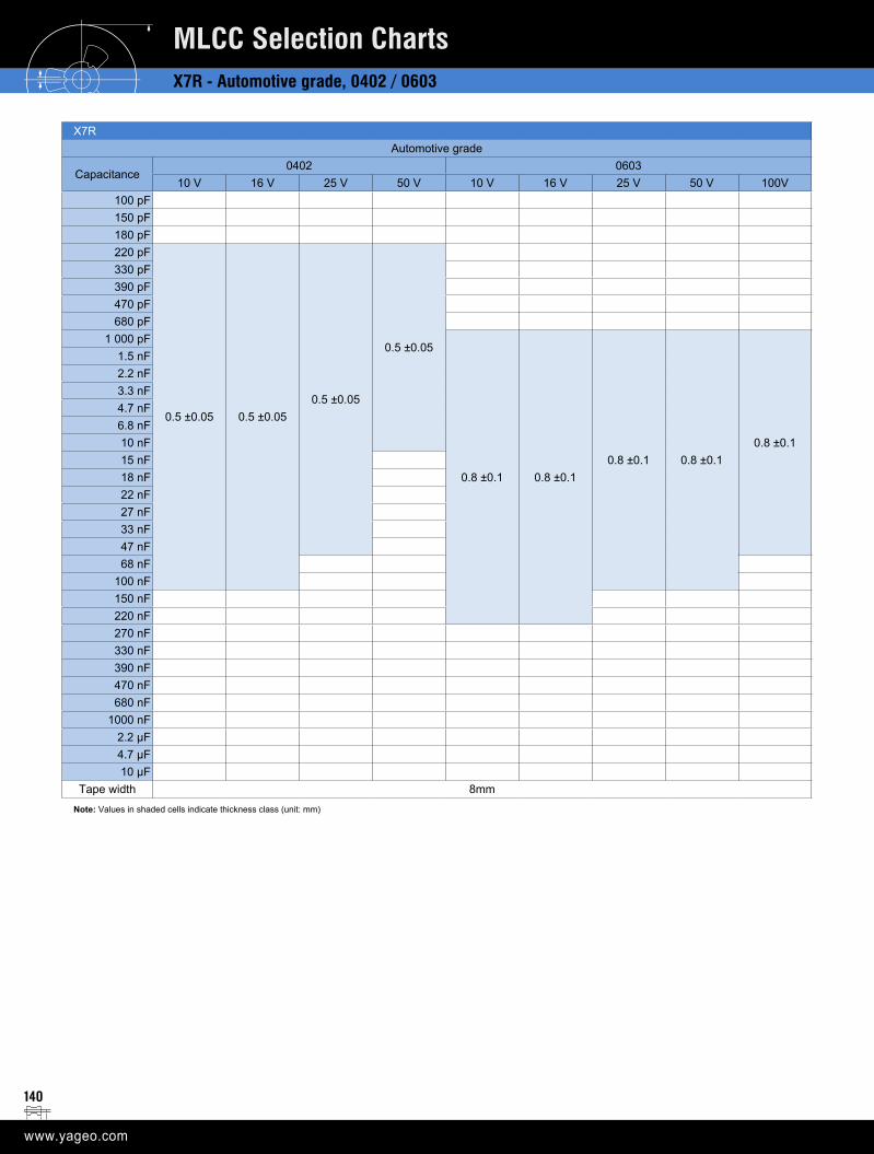
140
X7R - Automotive grade, 0402 / 0603
MLCC Selection Charts
X7RAutomotive grade
Capacitance0402 0603
10 V 16 V 25 V 50 V 10 V 16 V 25 V 50 V 100V100 pF150 pF180 pF220 pF
0.5 ±0.05 0.5 ±0.050.5 ±0.05
0.5 ±0.05
330 pF390 pF470 pF680 pF
1 000 pF
0.8 ±0.1 0.8 ±0.10.8 ±0.1 0.8 ±0.1
0.8 ±0.1
1.5 nF2.2 nF3.3 nF4.7 nF6.8 nF10 nF15 nF18 nF22 nF27 nF33 nF47 nF68 nF
100 nF150 nF220 nF270 nF330 nF390 nF470 nF680 nF
1000 nF 2.2 μF4.7 μF10 μF
Tape width 8mmNote: Values in shaded cells indicate thickness class (unit: mm)
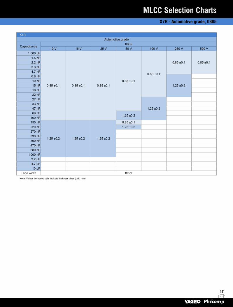
141
X7R - Automotive grade, 0805
MLCC Selection Charts
X7RAutomotive grade
Capacitance0805
10 V 16 V 25 V 50 V 100 V 250 V 500 V1 000 pF
0.85 ±0.1 0.85 ±0.1 0.85 ±0.10.85 ±0.1
0.85 ±0.1
0.85 ±0.1 0.85 ±0.11.5 nF2.2 nF3.3 nF4.7 nF6.8 nF
1.25 ±0.210 nF15 nF18 nF22 nF27 nF
1.25 ±0.233 nF47 nF68 nF
1.25 ±0.2100 nF150 nF
1.25 ±0.2 1.25 ±0.2 1.25 ±0.2
0.85 ±0.1220 nF 1.25 ±0.2270 nF330 nF390 nF470 nF680 nF
1000 nF2.2 μF4.7 μF10 μF
Tape width 8mm
Note: Values in shaded cells indicate thickness class (unit: mm)
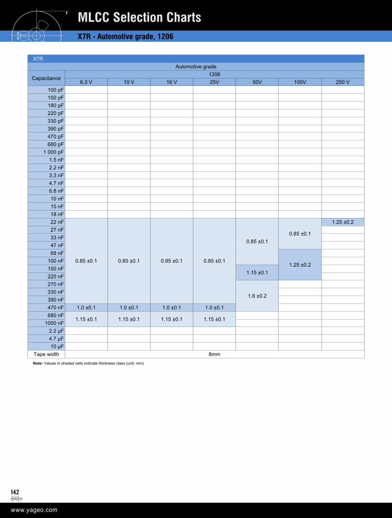
142
X7R - Automotive grade, 1206
MLCC Selection Charts
X7RAutomotive grade
Capacitance1206
6.3 V 10 V 16 V 25V 50V 100V 250 V100 pF150 pF180 pF220 pF330 pF390 pF470 pF680 pF
1 000 pF1.5 nF2.2 nF3.3 nF4.7 nF6.8 nF10 nF15 nF18 nF22 nF
0.85 ±0.1 0.85 ±0.1 0.85 ±0.1 0.85 ±0.1
0.85 ±0.10.85 ±0.1
1.25 ±0.227 nF33 nF47 nF68 nF
1.25 ±0.2100 nF150 nF
1.15 ±0.1220 nF270 nF
1.6 ±0.2330 nF390 nF470 nF 1.0 ±0.1 1.0 ±0.1 1.0 ±0.1 1.0 ±0.1680 nF
1.15 ±0.1 1.15 ±0.1 1.15 ±0.1 1.15 ±0.11000 nF
2.2 μF4.7 μF10 μF
Tape width 8mmNote: Values in shaded cells indicate thickness class (unit: mm)
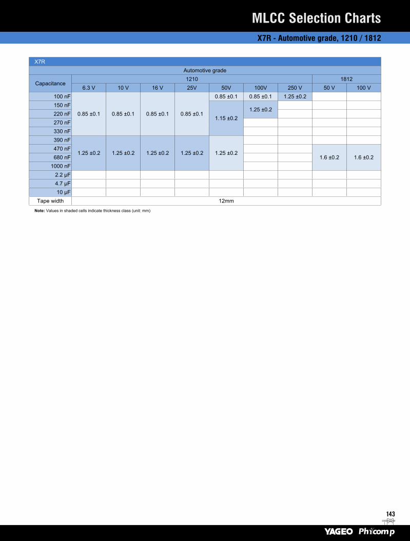
143
X7R - Automotive grade, 1210 / 1812
MLCC Selection Charts
X7RAutomotive grade
Capacitance1210 1812
6.3 V 10 V 16 V 25V 50V 100V 250 V 50 V 100 V100 nF
0.85 ±0.1 0.85 ±0.1 0.85 ±0.1 0.85 ±0.1
0.85 ±0.1 0.85 ±0.1 1.25 ±0.2150 nF
1.15 ±0.21.25 ±0.2
220 nF270 nF330 nF390 nF
1.25 ±0.2 1.25 ±0.2 1.25 ±0.2 1.25 ±0.2 1.25 ±0.2470 nF
1.6 ±0.2 1.6 ±0.2680 nF1000 nF
2.2 μF4.7 μF10 μF
Tape width 12mm
Note: Values in shaded cells indicate thickness class (unit: mm)
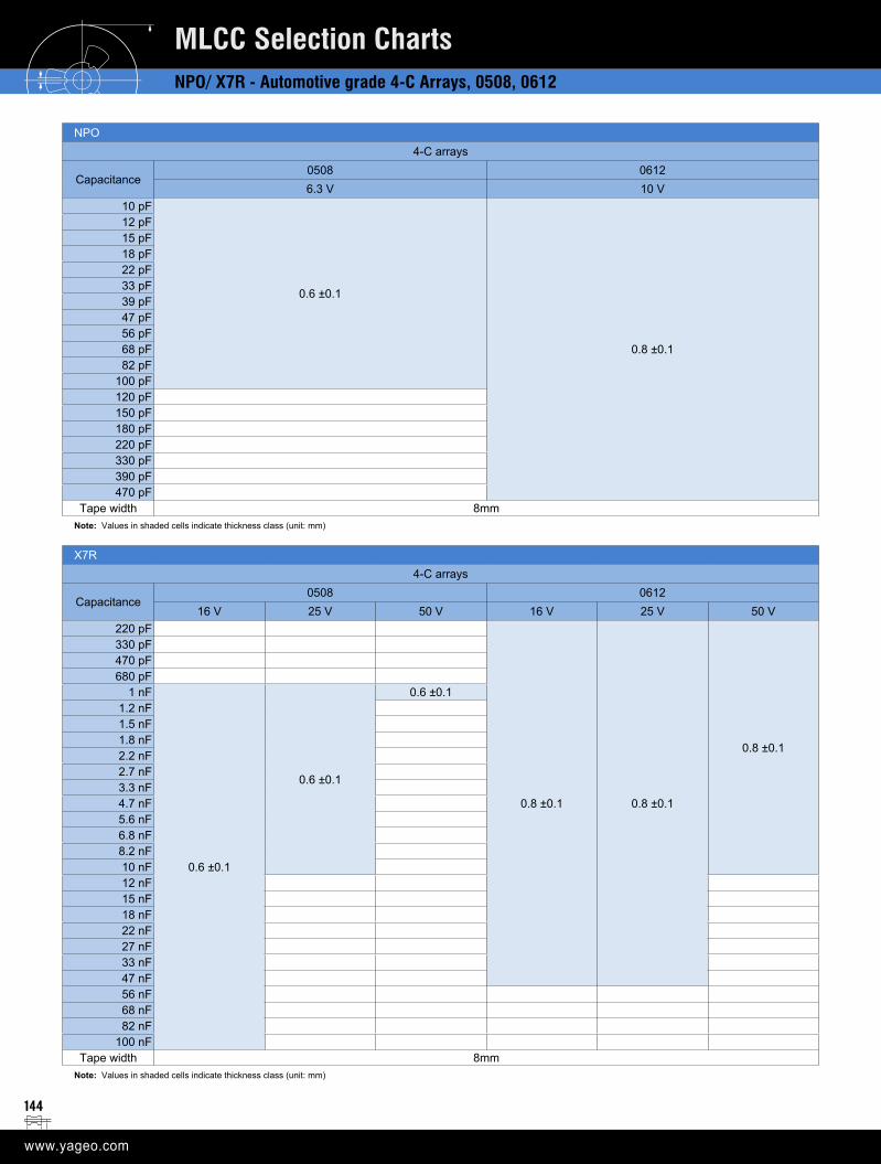
144
NPO/ X7R - Automotive grade 4-C Arrays, 0508, 0612
MLCC Selection Charts
NPO4-C arrays
Capacitance0508 06126.3 V 10 V
10 pF
0.6 ±0.1
0.8 ±0.1
12 pF15 pF18 pF22 pF33 pF39 pF47 pF56 pF68 pF82 pF
100 pF120 pF150 pF180 pF220 pF330 pF390 pF470 pF
Tape width 8mmNote: Values in shaded cells indicate thickness class (unit: mm)
X7R4-C arrays
Capacitance0508 0612
16 V 25 V 50 V 16 V 25 V 50 V220 pF
0.8 ±0.1 0.8 ±0.1
0.8 ±0.1
330 pF470 pF680 pF
1 nF
0.6 ±0.1
0.6 ±0.1
0.6 ±0.11.2 nF1.5 nF1.8 nF2.2 nF2.7 nF3.3 nF4.7 nF5.6 nF6.8 nF8.2 nF10 nF12 nF15 nF18 nF22 nF27 nF33 nF47 nF56 nF68 nF82 nF
100 nFTape width 8mm
Note: Values in shaded cells indicate thickness class (unit: mm)
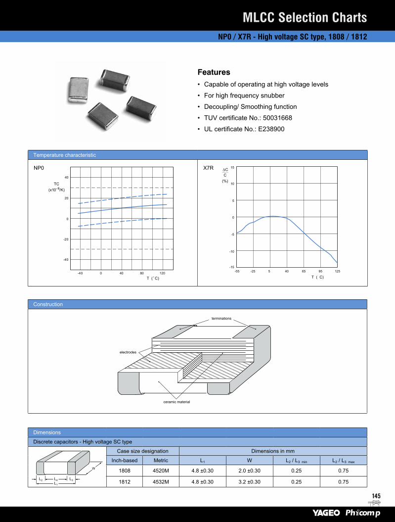
145
NP0 / X7R - High voltage SC type, 1808 / 1812
MLCC Selection Charts
Temperature characteristic
NP0 X7R
Construction
Dimensions
Discrete capacitors - High voltage SC type
L2 L3L4L1
W
Case size designation Dimensions in mm
Inch-based Metric L1 W L2 / L3 min L2 / L3 max
1808 4520M 4.8 ±0.30 2.0 ±0.30 0.25 0.75
1812 4532M 4.8 ±0.30 3.2 ±0.30 0.25 0.75
Features• Capable of operating at high voltage levels
• For high frequency snubber
• Decoupling/ Smoothing function
• TUV certificate No.: 50031668
• UL certificate No.: E238900
40
0
20
0 40 80 120T ( C)
TC(x10 /K)- 6
-40
-40
-20
15
5
-15-25-55 5 40 9565 125
10
-10
∆CC
(%)
-5
0
T ( C)
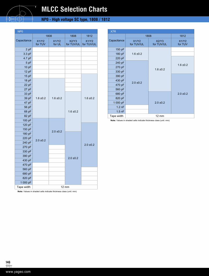
146
NP0 - High voltage SC type, 1808 / 1812
MLCC Selection Charts
NP0
Capacitance1808 1808 1812
X1/Y2 for TUV
X1/Y2 for UL
X2/Y3 for TUV/UL
X1/Y2 for TUV/UL
2 pF3.3 pF4.7 pF
5 pF10 pF12 pF15 pF
1.6 ±0.2
18 pF
1.6 ±0.2 1.6 ±0.2
22 pF27 pF33 pF
1.6 ±0.2
39 pF47 pF56 pF68 pF82 pF
100 pF
2.0 ±0.2
2.0 ±0.2
120 pF
2.0 ±0.2
150 pF180 pF
2.0 ±0.2
220 pF240 pF270 pF330 pF390 pF430 pF470 pF560 pF680 pF820 pF
1 000 pFTape width 12 mmNote: Values in shaded cells indicate thickness class (unit: mm)
X7R
Capacitance1808 1812
X1/Y2 for TUV/UL
X2/Y3 for TUV/UL
X1/Y2 for TUV
150 pF1.6 ±0.2
1.6 ±0.2
180 pF220 pF
1.6 ±0.2240 pF
2.0 ±0.2
270 pF330 pF390 pF
2.0 ±0.2
430 pF470 pF560 pF680 pF
2.0 ±0.2820 pF
1 000 pF1.2 nF1.5 nF
Tape width 12 mmNote: Values in shaded cells indicate thickness class (unit: mm)
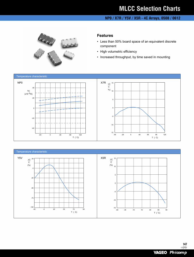
147
MLCC Selection ChartsNP0 / X7R / Y5V / X5R - 4C Arrays, 0508 / 0612
Temperature characteristic
NP0 X7R
Temperature characteristic
Y5V X5R
Features• Less than 50% board space of an equivalent discrete
component
• High volumetric efficiency
• Increased throughput, by time saved in mounting
40
0
20
0 40 80 120T ( C)
TC(x10 /K)- 6
-40
-40
-20
15
5
-15-25-55 5 40 9565 125
10
-10
∆CC
(%)
-5
0
T ( C)
0
-100-5-30 20 55 9570
25
-75
C(%)
-50
-25
T ( C)
∆C15
5
-15-35-60 -10 15 6540 90
10
-10
C(%)
-5
0
T ( C)
∆C
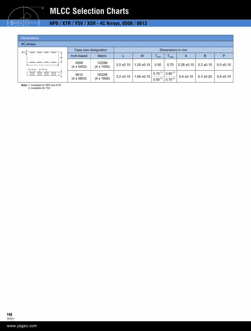
148
MLCC Selection ChartsNP0 / X7R / Y5V / X5R - 4C Arrays, 0508 / 0612
Dimensions
4C arrays
L
PA
T
B
W
Case size designation Dimensions in mm
Inch-based Metric L W Tmin Tmax A B P
0508 (4 x 0402)
1220M (4 x 1005) 2.0 ±0.15 1.25 ±0.15 0.50 0.70 0.28 ±0.10 0.2 ±0.10 0.5 ±0.10
0612 (4 x 0603)
1632M (4 x 1608) 3.2 ±0.15 1.60 ±0.15
0.70 (1) 0.90 (1)
0.4 ±0.10 0.3 ±0.20 0.8 ±0.100.50 (2) 0.70 (2)
Note: 1. Available for NP0 and X7R 2. Available for Y5V
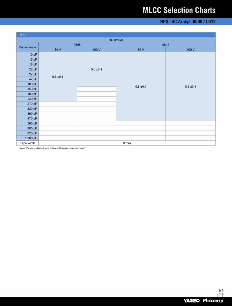
149
MLCC Selection ChartsNP0 - 4C Arrays, 0508 / 0612
NP04C arrays
Capacitance0508 0612
50 V 100 V 50 V 100 V10 pF
0.6 ±0.1
0.6 ±0.1
0.8 ±0.1 0.8 ±0.1
15 pF18 pF22 pF27 pF47 pF
100 pF150 pF180 pF220 pF270 pF330 pF390 pF470 pF560 pF680 pF820 pF
1 000 pFTape width 8 mmNote: Values in shaded cells indicate thickness class (unit: mm)
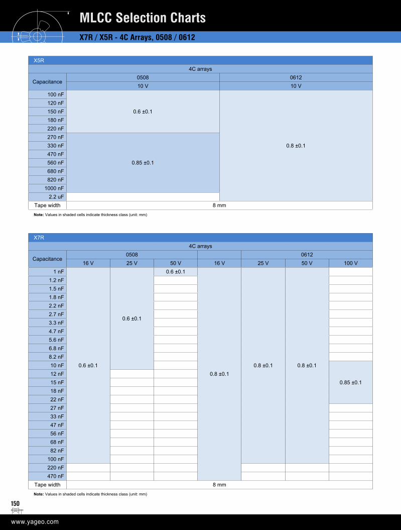
150
MLCC Selection ChartsX7R / X5R - 4C Arrays, 0508 / 0612
X5R4C arrays
Capacitance0508 061210 V 10 V
100 nF
0.6 ±0.1
0.8 ±0.1
120 nF150 nF180 nF220 nF270 nF
0.85 ±0.1
330 nF470 nF560 nF680 nF820 nF
1000 nF2.2 uF
Tape width 8 mm
Note: Values in shaded cells indicate thickness class (unit: mm)
X7R4C arrays
Capacitance0508 0612
16 V 25 V 50 V 16 V 25 V 50 V 100 V1 nF
0.6 ±0.1
0.6 ±0.1
0.6 ±0.1
0.8 ±0.10.8 ±0.1 0.8 ±0.1
1.2 nF1.5 nF1.8 nF2.2 nF2.7 nF3.3 nF4.7 nF5.6 nF6.8 nF8.2 nF10 nF
0.85 ±0.112 nF15 nF18 nF22 nF27 nF33 nF47 nF56 nF68 nF82 nF
100 nF220 nF470 nF
Tape width 8 mm
Note: Values in shaded cells indicate thickness class (unit: mm)
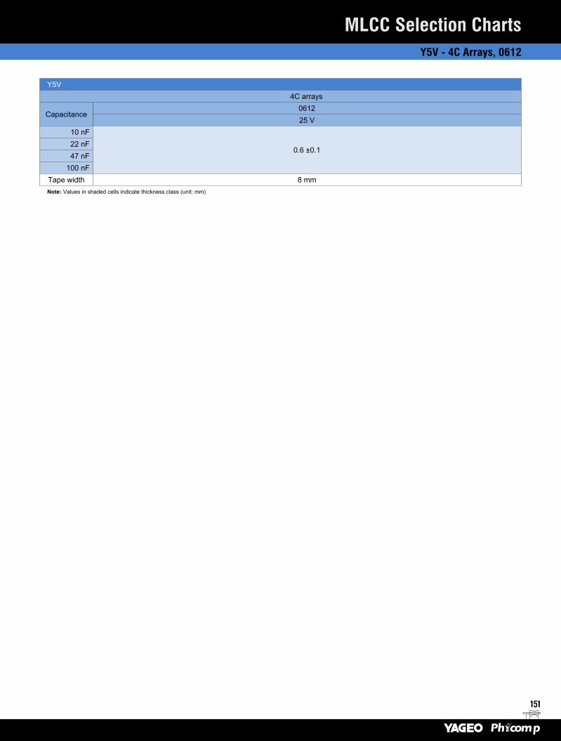
151
MLCC Selection ChartsY5V - 4C Arrays, 0612
Y5V 4C arrays
Capacitance061225 V
10 nF
0.6 ±0.122 nF47 nF
100 nFTape width 8 mmNote: Values in shaded cells indicate thickness class (unit: mm)
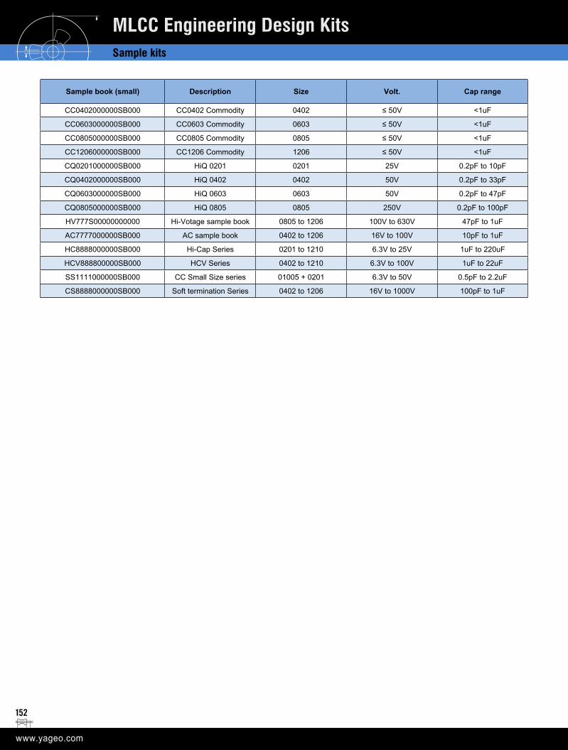
152
MLCC Engineering Design KitsSample kits
Sample book (small) Description Size Volt. Cap range
CC0402000000SB000 CC0402 Commodity 0402 ≤ 50V <1uF
CC0603000000SB000 CC0603 Commodity 0603 ≤ 50V <1uF
CC0805000000SB000 CC0805 Commodity 0805 ≤ 50V <1uF
CC1206000000SB000 CC1206 Commodity 1206 ≤ 50V <1uF
CQ0201000000SB000 HiQ 0201 0201 25V 0.2pF to 10pF
CQ0402000000SB000 HiQ 0402 0402 50V 0.2pF to 33pF
CQ0603000000SB000 HiQ 0603 0603 50V 0.2pF to 47pF
CQ0805000000SB000 HiQ 0805 0805 250V 0.2pF to 100pF
HV777S00000000000 Hi-Votage sample book 0805 to 1206 100V to 630V 47pF to 1uF
AC7777000000SB000 AC sample book 0402 to 1206 16V to 100V 10pF to 1uF
HC8888000000SB000 Hi-Cap Series 0201 to 1210 6.3V to 25V 1uF to 220uF
HCV888800000SB000 HCV Series 0402 to 1210 6.3V to 100V 1uF to 22uF
SS1111000000SB000 CC Small Size series 01005 + 0201 6.3V to 50V 0.5pF to 2.2uF
CS8888000000SB000 Soft termination Series 0402 to 1206 16V to 1000V 100pF to 1uF
SMD CERAMIC EMI FILTER CAPACITORS X2Y ® PRODUCTS
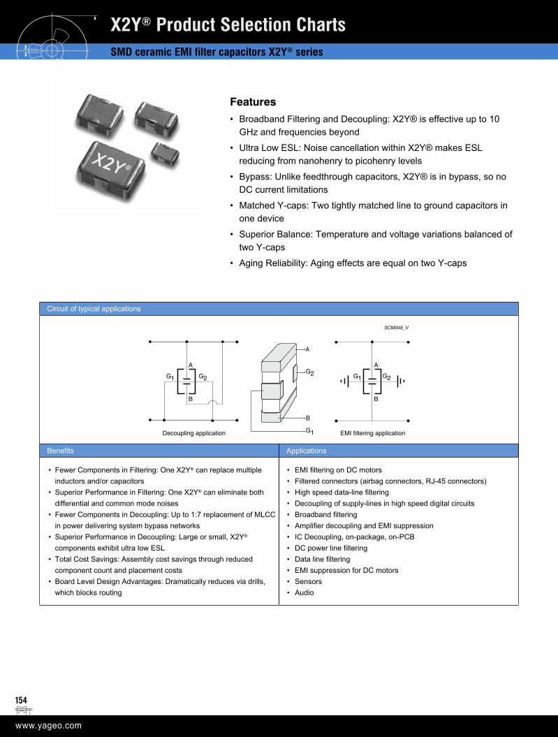
154
X2Y® Product Selection ChartsSMD ceramic EMI filter capacitors X2Y® series
Circuit of typical applications
SCM049_V
Decoupling application EMI filtering application
A
G2
B
B
A
G1 G2
B
A
G2
G1
G1
Benefits Applications
• Fewer Components in Filtering: One X2Y® can replace multiple inductors and/or capacitors
• Superior Performance in Filtering: One X2Y® can eliminate both differential and common mode noises
• Fewer Components in Decoupling: Up to 1:7 replacement of MLCC in power delivering system bypass networks
• Superior Performance in Decoupling: Large or small, X2Y® components exhibit ultra low ESL
• Total Cost Savings: Assembly cost savings through reduced component count and placement costs
• Board Level Design Advantages: Dramatically reduces via drills, which blocks routing
• EMI filtering on DC motors• Filtered connectors (airbag connectors, RJ-45 connectors)• High speed data-line filtering• Decoupling of supply-lines in high speed digital circuits• Broadband filtering• Amplifier decoupling and EMI suppression• IC Decoupling, on-package, on-PCB• DC power line filtering• Data line filtering• EMI suppression for DC motors• Sensors• Audio
Features• Broadband Filtering and Decoupling: X2Y® is effective up to 10
GHz and frequencies beyond
• Ultra Low ESL: Noise cancellation within X2Y® makes ESL reducing from nanohenry to picohenry levels
• Bypass: Unlike feedthrough capacitors, X2Y® is in bypass, so no DC current limitations
• Matched Y-caps: Two tightly matched line to ground capacitors in one device
• Superior Balance: Temperature and voltage variations balanced of two Y-caps
• Aging Reliability: Aging effects are equal on two Y-caps
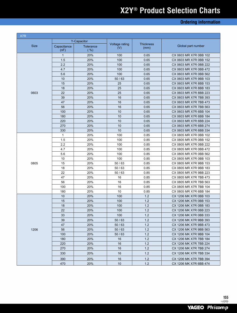
155
X7R
SizeY-Capacitor
Voltage rating (V)
Thickness(mm) Global part numberCapacitance
(nF)Tolerance
( %)
0603
1 20% 100 0.65 CX 0603 MR X7R 0BB 1021.5 20% 100 0.65 CX 0603 MR X7R 0BB 1522.2 20% 100 0.65 CX 0603 MR X7R 0BB 2224.7 20% 100 0.65 CX 0603 MR X7R 0BB 4725.6 20% 100 0.65 CX 0603 MR X7R 0BB 56210 20% 50 / 63 0.65 CX 0603 MR X7R 9BB 10315 20% 25 0.65 CX 0603 MR X7R 8BB 15318 20% 25 0.65 CX 0603 MR X7R 8BB 18322 20% 25 0.65 CX 0603 MR X7R 8BB 22339 20% 16 0.65 CX 0603 MR X7R 7BB 39347 20% 16 0.65 CX 0603 MR X7R 7BB 47356 20% 16 0.65 CX 0603 MR X7R 7BB 563100 20% 10 0.65 CX 0603 MR X7R 6BB 104180 20% 10 0.65 CX 0603 MR X7R 6BB 184220 20% 10 0.65 CX 0603 MR X7R 6BB 224270 20% 10 0.65 CX 0603 MR X7R 6BB 274330 20% 10 0.65 CX 0603 MR X7R 6BB 334
0805
1 20% 100 0.85 CX 0805 MR X7R 0BB 1021.5 20% 100 0.85 CX 0805 MR X7R 0BB 1522.2 20% 100 0.85 CX 0805 MR X7R 0BB 2224.7 20% 100 0.85 CX 0805 MR X7R 0BB 4725.6 20% 100 0.85 CX 0805 MR X7R 0BB 56210 20% 100 0.85 CX 0805 MR X7R 0BB 10315 20% 50 / 63 0.85 CX 0805 MR X7R 9BB 15318 20% 50 / 63 0.85 CX 0805 MR X7R 9BB 18322 20% 50 / 63 0.85 CX 0805 MR X7R 9BB 22347 20% 16 0.85 CX 0805 MR X7R 7BB 47356 20% 16 0.85 CX 0805 MR X7R 7BB 563100 20% 16 0.85 CX 0805 MR X7R 7BB 104180 20% 10 0.85 CX 0805 MR X7R 6BB 184
1206
10 20% 100 1.2 CX 1206 MK X7R 0BB 10315 20% 100 1.2 CX 1206 MK X7R 0BB 15318 20% 100 1.2 CX 1206 MK X7R 0BB 18322 20% 100 1.2 CX 1206 MK X7R 0BB 22333 20% 100 1.2 CX 1206 MK X7R 0BB 33339 20% 50 / 63 1.2 CX 1206 MK X7R 9BB 39347 20% 50 / 63 1.2 CX 1206 MK X7R 9BB 47356 20% 50 / 63 1.2 CX 1206 MK X7R 9BB 563100 20% 50 / 63 1.2 CX 1206 MK X7R 9BB 104180 20% 16 1.2 CX 1206 MK X7R 7BB 184220 20% 16 1.2 CX 1206 MK X7R 7BB 224270 20% 16 1.2 CX 1206 MK X7R 7BB 274330 20% 16 1.2 CX 1206 MK X7R 7BB 334
390 20% 16 1.2 CX 1206 MK X7R 7BB 394470 20% 10 1.2 CX 1206 MK X7R 6BB 474
X2Y® Product Selection ChartsOrdering information
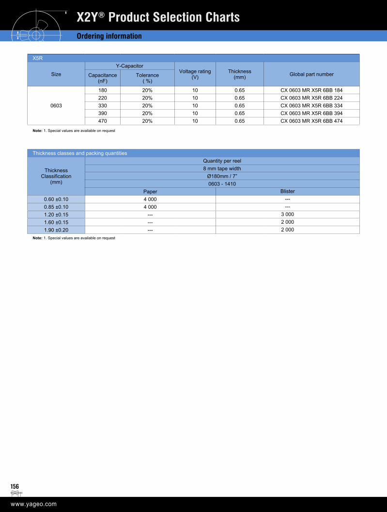
156
X2Y® Product Selection ChartsOrdering information
X5R
SizeY-Capacitor
Voltage rating (V)
Thickness(mm) Global part numberCapacitance
(nF)Tolerance
( %)
0603
180 20% 10 0.65 CX 0603 MR X5R 6BB 184220 20% 10 0.65 CX 0603 MR X5R 6BB 224330 20% 10 0.65 CX 0603 MR X5R 6BB 334390 20% 10 0.65 CX 0603 MR X5R 6BB 394470 20% 10 0.65 CX 0603 MR X5R 6BB 474
Note: 1. Special values are available on request
Thickness classes and packing quantities
Thickness Classification
(mm)
Quantity per reel8 mm tape width
Ø180mm / 7”0603 - 1410
Paper Blister0.60 ±0.10 4 000 ---0.85 ±0.10 4 000 ---1.20 ±0.15 --- 3 0001.60 ±0.15 --- 2 0001.90 ±0.20 --- 2 000
Note: 1. Special values are available on request
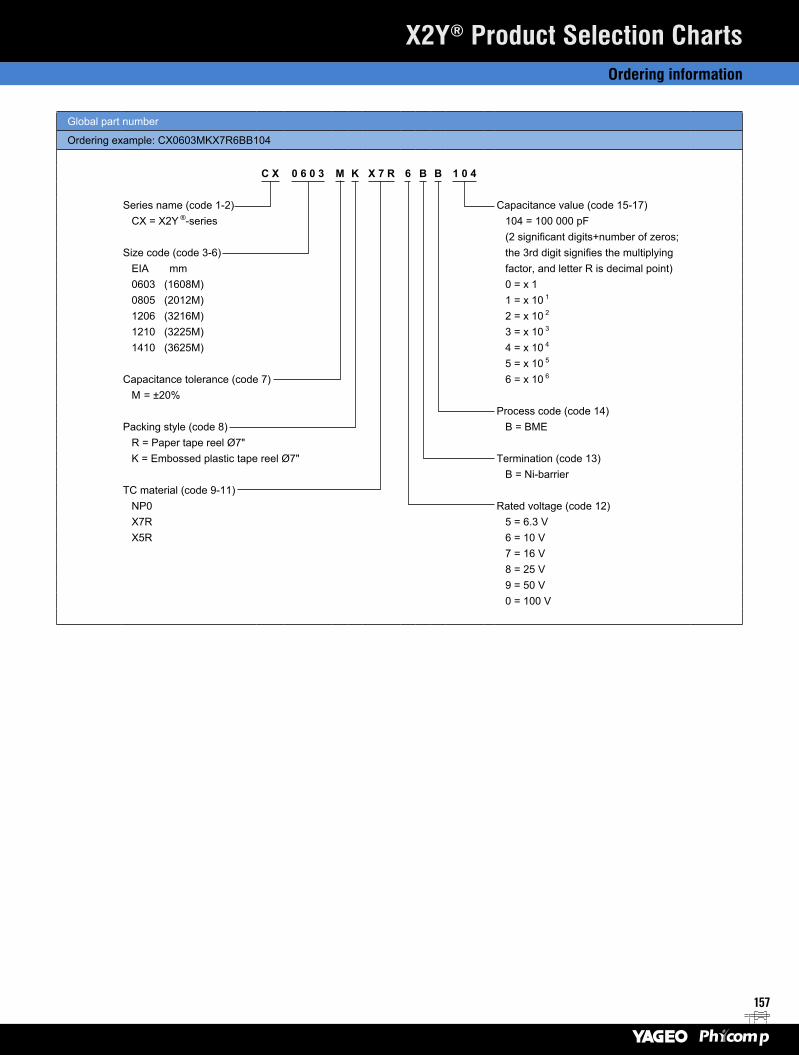
157
Global part number
Ordering example: CX0603MKX7R6BB104
C X 0 6 0 3 M K X 7 R 6 B B 1 0 4
Series name (code 1-2) Capacitance value (code 15-17)CX = X2Y ®-series 104 = 100 000 pF
(2 significant digits+number of zeros; Size code (code 3-6) the 3rd digit signifies the multiplying
EIA mm factor, and letter R is decimal point)0603 (1608M) 0 = x 10805 (2012M) 1 = x 10 1
1206 (3216M) 2 = x 10 2
1210 (3225M) 3 = x 10 3
1410 (3625M) 4 = x 10 4
5 = x 10 5
Capacitance tolerance (code 7) 6 = x 10 6
M = ±20%Process code (code 14)
Packing style (code 8) B = BMER = Paper tape reel Ø7"K = Embossed plastic tape reel Ø7" Termination (code 13)
B = Ni-barrierTC material (code 9-11)
NP0 Rated voltage (code 12)X7R 5 = 6.3 VX5R 6 = 10 V
7 = 16 V8 = 25 V9 = 50 V0 = 100 V
X2Y® Product Selection ChartsOrdering information

WIRELESS COMPONENTS
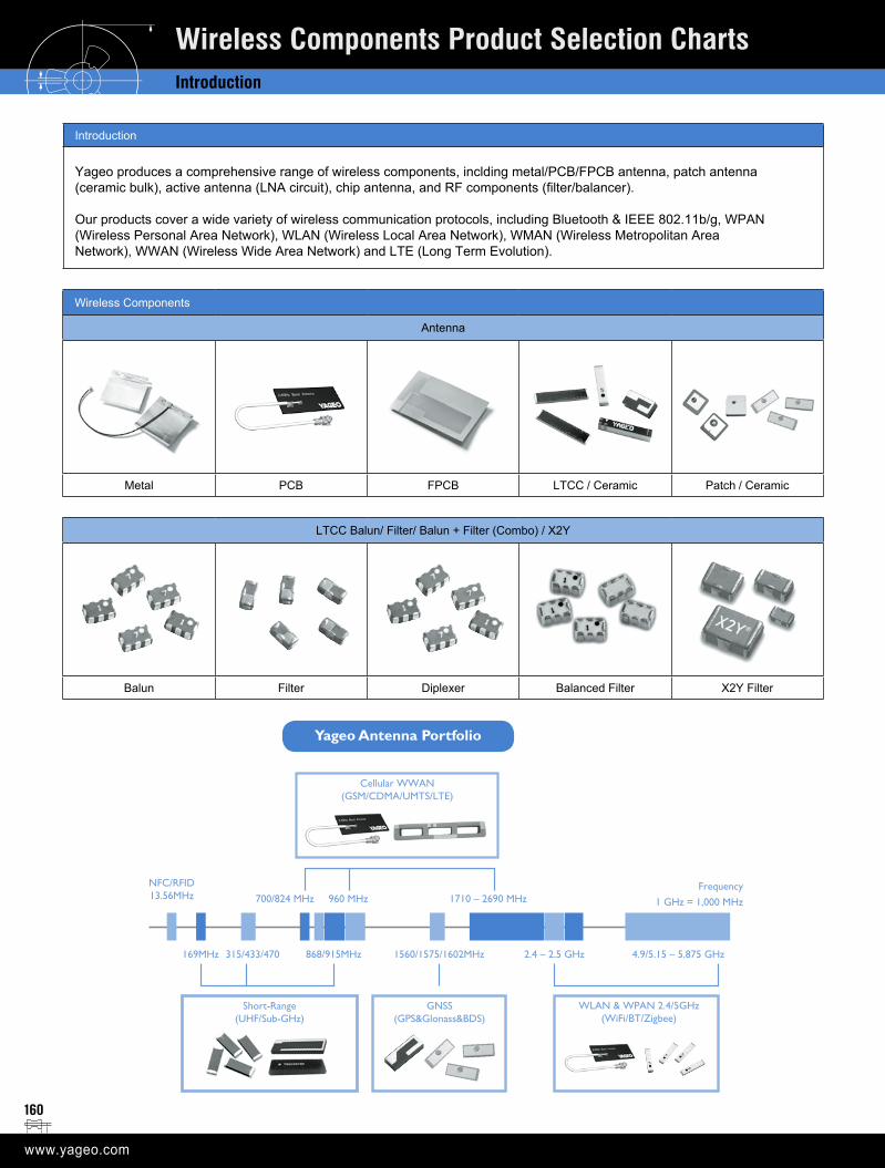
160
Wireless Components Product Selection ChartsIntroduction
Wireless Components
Antenna
Metal PCB FPCB LTCC / Ceramic Patch / Ceramic
LTCC Balun/ Filter/ Balun + Filter (Combo) / X2Y
Balun Filter Diplexer Balanced Filter X2Y Filter
Yageo Antenna Portfolio
Introduction
Yageo produces a comprehensive range of wireless components, inclding metal/PCB/FPCB antenna, patch antenna (ceramic bulk), active antenna (LNA circuit), chip antenna, and RF components (filter/balancer).
Our products cover a wide variety of wireless communication protocols, including Bluetooth & IEEE 802.11b/g, WPAN(Wireless Personal Area Network), WLAN (Wireless Local Area Network), WMAN (Wireless Metropolitan AreaNetwork), WWAN (Wireless Wide Area Network) and LTE (Long Term Evolution).
NFC/RFID13.56MHz
Short-Range (UHF/Sub-GHz)
GNSS(GPS&Glonass&BDS)
WLAN & WPAN 2.4/5GHz (WiFi/BT/Zigbee)
700/824 MHz 960 MHz
2.4 – 2.5 GHz 4.9/5.15 – 5.875 GHz169MHz 315/433/470 868/915MHz 1560/1575/1602MHz
1710 – 2690 MHz 1 GHz = 1,000 MHzFrequency
Cellular WWAN (GSM/CDMA/UMTS/LTE)
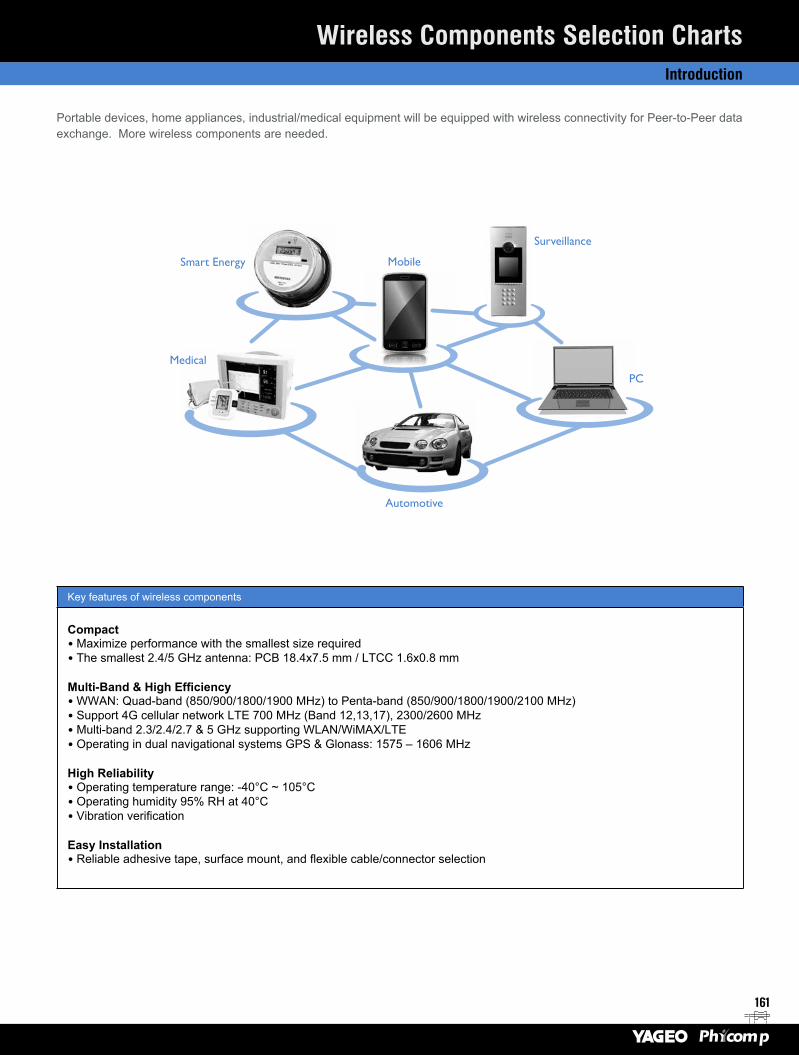
161
Key features of wireless components
Compact• Maximize performance with the smallest size required• The smallest 2.4/5 GHz antenna: PCB 18.4x7.5 mm / LTCC 1.6x0.8 mm
Multi-Band & High Efficiency• WWAN: Quad-band (850/900/1800/1900 MHz) to Penta-band (850/900/1800/1900/2100 MHz)• Support 4G cellular network LTE 700 MHz (Band 12,13,17), 2300/2600 MHz • Multi-band 2.3/2.4/2.7 & 5 GHz supporting WLAN/WiMAX/LTE• Operating in dual navigational systems GPS & Glonass: 1575 – 1606 MHz
High Reliability• Operating temperature range: -40°C ~ 105°C• Operating humidity 95% RH at 40°C• Vibration verification
Easy Installation• Reliable adhesive tape, surface mount, and flexible cable/connector selection
Wireless Components Selection ChartsIntroduction
Portable devices, home appliances, industrial/medical equipment will be equipped with wireless connectivity for Peer-to-Peer data exchange. More wireless components are needed.
Mobile
PC
Surveillance
Automotive
Medical
Smart Energy
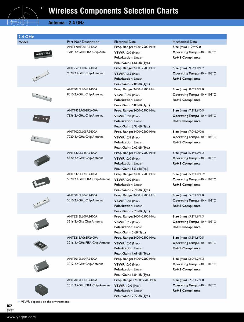
162
Wireless Components Selection ChartsAntenna - 2.4 GHz
2.4 GHzModel Part No./ Description Electrical Data Mechanical Data
ANT1204F001R2400A
1204 2.4GHz PIFA Chip Ante
Freq. Range: 2400~2500 MHz Size (mm) : 12*4*2.0
VSWR*: 2.0 (Max) Operating Temp.: -40 ~ 105°C
Polarization: Linear RoHS Compliance
Peak Gain : 6.66 dBi(Typ.)
ANT9520LL06R2400A
9520 2.4GHz Chip Antenna
Freq. Range: 2400~2500 MHz Size (mm) : 9.5*2.0*1.2
VSWR*: 2.5 (Max) Operating Temp.: -40 ~ 105°C
Polarization: Linear RoHS Compliance
Peak Gain : 2.85 dBi(Typ.)
ANT8010LL04R2400A
8010 2.4GHz Chip Antenna
Freq. Range: 2400~2500 MHz Size (mm) : 8.0*1.0*1.0
VSWR*: 2.0 (Max) Operating Temp.: -40 ~ 105°C
Polarization: Linear RoHS Compliance
Peak Gain : 5.88 dBi(Typ.)
ANT7836A003R2400A
7836 2.4GHz Chip Antenna
Freq. Range: 2400~2500 MHz Size (mm) : 7.8*3.6*0.5
VSWR*: 2.0 (Max) Operating Temp.: -40 ~ 105°C
Polarization: Linear RoHS Compliance
Peak Gain : 3.93 dBi(Typ.)
ANT7020LL05R2400A
7020 2.4GHz Chip Antenna
Freq. Range: 2400~2500 MHz Size (mm) : 7.0*2.0*0.8
VSWR*: 2.8 (Max) Operating Temp.: -40 ~ 105°C
Polarization: Linear RoHS Compliance
Peak Gain : 2.62 dBi(Typ.)
ANT5320LL45R2400A
5320 2.4GHz Chip Antenna
Freq. Range: 2400~2500 MHz Size (mm) : 5.3*2.0*1.2
VSWR*: 2.0 (Max) Operating Temp.: -40 ~ 105°C
Polarization: Linear RoHS Compliance
Peak Gain : 5.5 dBi(Typ.)
ANT5320LL24R2400A
5320 2.4GHz PIFA Chip Antenna
Freq. Range: 2400~2500 MHz Size (mm) : 5.3*2.0*1.25
VSWR*: 2.0 (Max) Operating Temp.: -40 ~ 105°C
Polarization: Linear RoHS Compliance
Peak Gain : 2.78 dBi(Typ.)
ANT5010LL04R2400A
5010 2.4GHz Chip Antenna
Freq. Range: 2400~2500 MHz Size (mm) : 5.0*1.0*1.0
VSWR*: 2.8 (Max) Operating Temp.: -40 ~ 105°C
Polarization: Linear RoHS Compliance
Peak Gain : 2.28 dBi(Typ.)
ANT3216LL00R2400A
3216 2.4Ghz Chip Antenna
Freq. Range: 2400~2500 MHz Size (mm) : 3.2*1.6*1.3
VSWR*: 2.5 (Max) Operating Temp.: -40 ~ 105°C
Polarization: Linear RoHS Compliance
Peak Gain : 5 dBi(Typ.)
ANT3216A063R2400A
3216 2.4GHz PIFA Chip Antenna
Freq. Range: 2400~2500 MHz Size (mm) : 3.2*1.6*0.5
VSWR*: 2.0 (Max) Operating Temp.: -40 ~ 105°C
Polarization: Linear RoHS Compliance
Peak Gain : 1.69 dBi(Typ.)
ANT3012LL04R2400A
3012 2.4GHz Chip Antenna
Freq. Range: 2400~2500 MHz Size (mm) : 3.0*1.2*1.2
VSWR*: 2.0 (Max) Operating Temp.: -40 ~ 105°C
Polarization: Linear RoHS Compliance
Peak Gain : 1.84 dBi(Typ.)
ANT2012LL13R2400A Freq. Range : 2400~2500 MHz Size (mm) : 2.0*1.2*1.0
2012 2.4GHz PIFA Chip Antenna VSWR*: 2.0 (Max) Operating Temp.: -40 ~ 105°C
Polarization: Linear RoHS Compliance
Peak Gain : 2.72 dBi(Typ.)
* VSWR depends on the environment
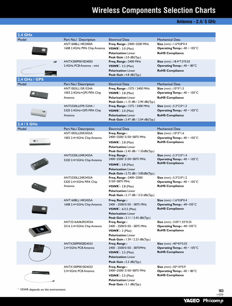
163
Wireless Components Selection ChartsAntenna - 2.4/ 5 GHz
2.4 GHzModel Part No./ Description Electrical Data Mechanical Data
ANT1608LL14R2400A Freq. Range : 2400~2500 MHz Size (mm) : 1.6*0.8*0.41608 2.4GHz PIFA Chip Antenna VSWR*: 3.0 (Max) Operating Temp.: -40 ~ 105°C
Polarization: Linear RoHS CompliancePeak Gain : 2.0 dBi(Typ.)
ANTX200P001B24003 Freq. Range : 2400 MHz Size (mm) : 18.4*7.5*0.552.4GHz PCB Antenna - mini VSWR*: 2.5 (Max) Operating Temp.: -40 ~ 80°C
Polarization: Linear RoHS CompliancePeak Gain : 4.8 dBi(Typ.)
2.4 GHz / GPS Model Part No./ Description Electrical Data Mechanical Data
ANT1003LL15R1524A Freq. Range : 1575 / 2400 MHz Size (mm) : 10*3*1.51003 2.4GHz+GPS PIFA Chip VSWR*: 2.8 (Max) Operating Temp.: -40 ~ 105°C
Antenna Polarization: Linear RoHS CompliancePeak Gain : 1.15 dBi / 2.90 dBi(Typ.)
ANT5320LL07R1524A / Freq. Range : 1575 / 2400 MHz Size (mm) : 5.3*2.0*1.25320 2.4GHz+GPS PIFA Chip VSWR*: 2.0 (Max) Operating Temp.: -40 ~ 105°C
Antenna Polarization: Linear RoHS CompliancePeak Gain : 2.47 dBi / 2.04 dBi(Typ.)
2.4 / 5 GHzModel Part No./ Description Electrical Data Mechanical Data
ANT1003LL05R2455A Freq. Range : 2400~2500/ 5150~5875 MHz
Size (mm) : 10*3*1.61003 2.4+5GHz Chip Antenna Operating Temp.: -40 ~ 105°C
VSWR*: 2.8 (Max) RoHS Compliance
Polarization: LinearPeak Gain : 2.45 dBi / 1.55dBi(Typ.)
ANT5320LL04R2455A
5320 2.4+5GHz Chip Antenna
Freq. Range : 2400~2500/ 5150~5875 MHz
Size (mm) : 5.3*2.0*1.4Operating Temp.: -40 ~ 105°CRoHS ComplianceVSWR*: 2.8 (Max)
Polarization: LinearPeak Gain : 2.72 dBi / 3.85dBi(Typ.)
ANT5320LL24R2455A Freq. Range : 2400~2500/ 5150~5875 MHz
Size (mm) : 5.3*2.0*1.25320 2.4+5GHz PIFA Chip Operating Temp.: -40 ~ 105°CAntenna VSWR*: 2.8 (Max) RoHS Compliance
Polarization: LinearPeak Gain : 2.17 dBi / 3.51dBi(Typ.)
ANT1608LL14R2455A Freq. Range : Size (mm) : 1.6*0.8*0.41608 2.4+5GHz Chip Antenna 2400 - 2500/5150 - 5875 MHz Operating Temp.: -40~105°C
VSWR*: 6/3.5 (Max) RoHS Compliance
Polarization: LinearPeak Gain : 3.11 / 3.43 dBi(Typ.)
ANT3216A063R2455A Freq. Range : Size (mm) : 3.05*1.55*0.553216 2.4+5GHz Chip Antenna 2400 - 2500/5150 - 5875 MHz Operating Temp.: -40~105°C
VSWR*: 2 (Max) RoHS Compliance
Polarization: LinearPeak Gain : 1.59 / 2.23 dBi(Typ.)
ANTX200P002B24553 Freq. Range : Size (mm) : 40*43*0.552.4+5GHz PCB Antenna 2400 - 2500/5150 - 5875MHz Operating Temp.: -40 ~ 105°C
VSWR*: 2.5 (Max) RoHS Compliance
Polarization: Linear
Peak Gain : 2.3 dBi(Typ.)
ANTX100P001B24553 Freq. Range : 2400~2500/ 5150~5875 MHz
Size (mm) : 50*10*0.92.4+5GHz PCB Antenna Operating Temp.: -40 ~ 80°C
VSWR*: 2.5 (Max) RoHS Compliance
Polarization: LinearPeak Gain : 5.1 dBi(Typ.)
* VSWR depends on the environment
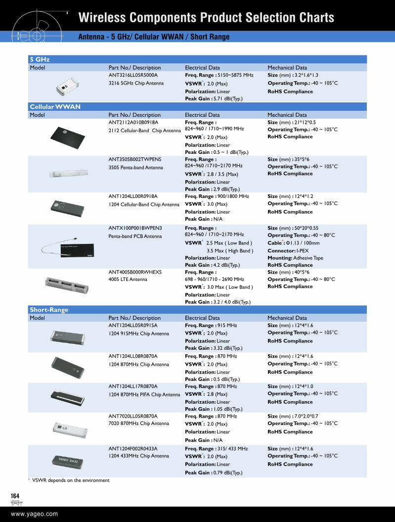
164
Wireless Components Product Selection ChartsAntenna - 5 GHz/ Cellular WWAN / Short Range
5 GHzModel Part No./ Description Electrical Data Mechanical Data
ANT3216LL05R5000A Freq. Range : 5150~5875 MHz Size (mm) : 3.2*1.6*1.3
3216 5GHz Chip Antenna VSWR*: 2.0 (Max) Operating Temp.: -40 ~ 105°C
Polarization: Linear RoHS CompliancePeak Gain : 5.71 dBi(Typ.)
* VSWR depends on the environmentCellular WWANModel Part No./ Description Electrical Data Mechanical Data
ANT2112A010B0918A
2112 Cellular-Band Chip Antenna
Freq. Range : 824~960 / 1710~1990 MHz
Size (mm) : 21*12*0.5Operating Temp.: -40 ~ 105°C
VSWR*: 2.0 (Max) RoHS Compliance
Polarization: LinearPeak Gain : 0.5 ~ 1 dBi(Typ.)
ANT3505B002TWPENS
3505 Penta-band Antenna
Freq. Range : 824~960 /1710~2170 MHz
Size (mm) : 35*5*6Operating Temp.: -40 ~ 105°C
VSWR*: 2.8 / 3.5 (Max) RoHS Compliance
Polarization: LinearPeak Gain : 2.9 dBi(Typ.)
ANT1204LL00R0918A
1204 Cellular-Band Chip Antenna
Freq. Range : 900/1800 MHz Size (mm) : 12*4*1.2VSWR*: 3.0 (Max) Operating Temp.: -40 ~ 105°C
Polarization: Linear RoHS CompliancePeak Gain : N/A
ANTX100P001BWPEN3
Penta-band PCB Antenna
Freq. Range : 824~960 / 1710~2170 MHz
Size (mm) : 50*20*0.55Operating Temp.: -40 ~ 80°C
VSWR* 2.5 Max ( Low Band ) Cable*: Φ1.13 / 100mm 3.5 Max ( High Band ) Connector: I-PEXPolarization: Linear Mounting: Adhesive TapePeak Gain : 4.2 dBi(Typ.) RoHS Compliance
ANT4005B000RWHEXS Freq. Range : Size (mm) : 40*5*64005 LTE Antenna 698 - 960/1710 - 2690 MHz Operating Temp.: -40 ~ 80°C
VSWR*: 3.0 Max ( Low Band ) RoHS Compliance
Polarization: LinearPeak Gain : 3.2 / 4.0 dBi(Typ.)
Short-RangeModel Part No./ Description Electrical Data Mechanical Data
ANT1204LL05R0915A
1204 915MHz Chip Antenna
Freq. Range : 915 MHz Size (mm) : 12*4*1.6VSWR*: 2.0 (Max) Operating Temp.: -40 ~ 105°C
Polarization: Linear RoHS CompliancePeak Gain : 3.32 dBi(Typ.)
ANT1204LL08R0870A
1204 870MHz Chip Antenna
Freq. Range : 870 MHz Size (mm) : 12*4*1.6
VSWR*: 2.0 (Max) Operating Temp.: -40 ~ 105°C
Polarization: Linear RoHS CompliancePeak Gain : 0.5 dBi(Typ.)
ANT1204LL17R0870A
1204 870MHz PIFA Chip Antenna
Freq. Range : 870 MHz Size (mm) : 12*4*1.0VSWR*: 2.8 (Max) Operating Temp.: -40 ~ 105°C
Polarization: Linear RoHS CompliancePeak Gain : 1.05 dBi(Typ.)
ANT7020LL05R0870A Freq. Range : 870 MHz Size (mm) : 7.0*2.0*0.77020 870MHz Chip Antenna VSWR*: 2.0 (Max) Operating Temp.: -40 ~ 105°C
Polarization: Linear RoHS Compliance
Peak Gain : N/A
ANT1204F002R0433A Freq. Range : 315/ 433 MHz Size (mm) : 12*4*1.61204 433MHz Chip Antenna VSWR*: 2.0 (Max) Operating Temp.: -40 ~ 105°C
Polarization: Linear RoHS Compliance
Peak Gain : 0.79 dBi(Typ.)* VSWR depends on the environment
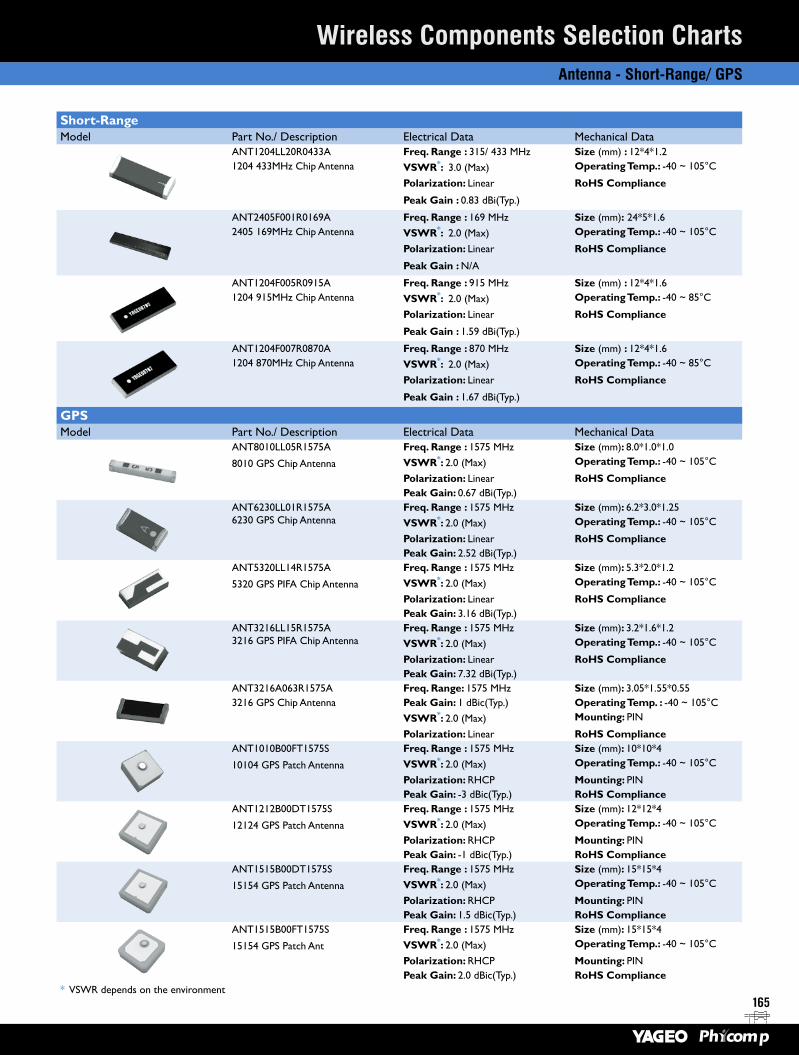
165
Wireless Components Selection ChartsAntenna - Short-Range/ GPS
Short-RangeModel Part No./ Description Electrical Data Mechanical Data
ANT1204LL20R0433A Freq. Range : 315/ 433 MHz Size (mm) : 12*4*1.21204 433MHz Chip Antenna VSWR*: 3.0 (Max) Operating Temp.: -40 ~ 105°C
Polarization: Linear RoHS Compliance
Peak Gain : 0.83 dBi(Typ.)
ANT2405F001R0169A Freq. Range : 169 MHz Size (mm): 24*5*1.62405 169MHz Chip Antenna VSWR*: 2.0 (Max) Operating Temp.: -40 ~ 105°C
Polarization: Linear RoHS Compliance
Peak Gain : N/A
ANT1204F005R0915A Freq. Range : 915 MHz Size (mm) : 12*4*1.61204 915MHz Chip Antenna VSWR*: 2.0 (Max) Operating Temp.: -40 ~ 85°C
Polarization: Linear RoHS Compliance
Peak Gain : 1.59 dBi(Typ.)
ANT1204F007R0870A Freq. Range : 870 MHz Size (mm) : 12*4*1.61204 870MHz Chip Antenna VSWR*: 2.0 (Max) Operating Temp.: -40 ~ 85°C
Polarization: Linear RoHS Compliance
Peak Gain : 1.67 dBi(Typ.)
GPSModel Part No./ Description Electrical Data Mechanical Data
ANT8010LL05R1575A
8010 GPS Chip Antenna
Freq. Range : 1575 MHz Size (mm): 8.0*1.0*1.0VSWR*: 2.0 (Max) Operating Temp.: -40 ~ 105°C
Polarization: Linear RoHS CompliancePeak Gain: 0.67 dBi(Typ.)
ANT6230LL01R1575A 6230 GPS Chip Antenna
Freq. Range : 1575 MHz Size (mm): 6.2*3.0*1.25VSWR*: 2.0 (Max) Operating Temp.: -40 ~ 105°C
Polarization: Linear RoHS CompliancePeak Gain: 2.52 dBi(Typ.)
ANT5320LL14R1575A
5320 GPS PIFA Chip Antenna
Freq. Range : 1575 MHz Size (mm): 5.3*2.0*1.2VSWR*: 2.0 (Max) Operating Temp.: -40 ~ 105°C
Polarization: Linear RoHS CompliancePeak Gain: 3.16 dBi(Typ.)
ANT3216LL15R1575A 3216 GPS PIFA Chip Antenna
Freq. Range : 1575 MHz Size (mm): 3.2*1.6*1.2VSWR*: 2.0 (Max) Operating Temp.: -40 ~ 105°C
Polarization: Linear RoHS CompliancePeak Gain: 7.32 dBi(Typ.)
ANT3216A063R1575A Freq. Range: 1575 MHz Size (mm): 3.05*1.55*0.553216 GPS Chip Antenna Peak Gain: 1 dBic(Typ.) Operating Temp. : -40 ~ 105°C
VSWR*: 2.0 (Max) Mounting: PIN
Polarization: Linear RoHS ComplianceANT1010B00FT1575S
10104 GPS Patch Antenna
Freq. Range : 1575 MHz Size (mm): 10*10*4VSWR*: 2.0 (Max) Operating Temp.: -40 ~ 105°C
Polarization: RHCP Mounting: PINPeak Gain: -3 dBic(Typ.) RoHS Compliance
ANT1212B00DT1575S
12124 GPS Patch Antenna
Freq. Range : 1575 MHz Size (mm): 12*12*4VSWR*: 2.0 (Max) Operating Temp.: -40 ~ 105°C
Polarization: RHCP Mounting: PINPeak Gain: -1 dBic(Typ.) RoHS Compliance
ANT1515B00DT1575S
15154 GPS Patch Antenna
Freq. Range : 1575 MHz Size (mm): 15*15*4VSWR*: 2.0 (Max) Operating Temp.: -40 ~ 105°C
Polarization: RHCP Mounting: PINPeak Gain: 1.5 dBic(Typ.) RoHS Compliance
ANT1515B00FT1575S
15154 GPS Patch Ant
Freq. Range : 1575 MHz Size (mm): 15*15*4VSWR*: 2.0 (Max) Operating Temp.: -40 ~ 105°C
Polarization: RHCP Mounting: PINPeak Gain: 2.0 dBic(Typ.) RoHS Compliance
* VSWR depends on the environment
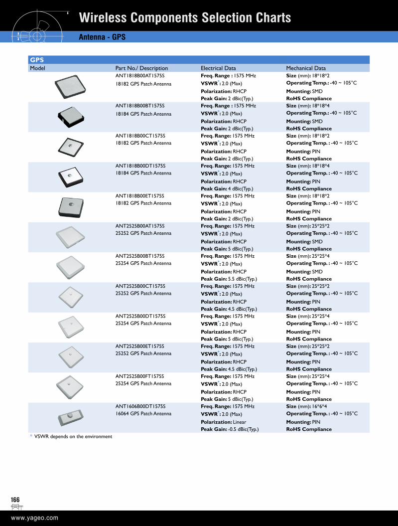
166
Wireless Components Selection ChartsAntenna - GPS
GPSModel Part No./ Description Electrical Data Mechanical Data
ANT1818B00AT1575S
18182 GPS Patch Antenna
Freq. Range : 1575 MHz Size (mm): 18*18*2VSWR*: 2.0 (Max) Operating Temp.: -40 ~ 105°C
Polarization: RHCP Mounting: SMDPeak Gain: 2 dBic(Typ.) RoHS Compliance
ANT1818B00BT1575S
18184 GPS Patch Antenna
Freq. Range : 1575 MHz Size (mm): 18*18*4VSWR*: 2.0 (Max) Operating Temp.: -40 ~ 105°C
Polarization: RHCP Mounting: SMDPeak Gain: 2 dBic(Typ.) RoHS Compliance
ANT1818B00CT1575S Freq. Range: 1575 MHz Size (mm): 18*18*218182 GPS Patch Antenna VSWR*: 2.0 (Max) Operating Temp. : -40 ~ 105°C
Polarization: RHCP Mounting: PINPeak Gain: 2 dBic(Typ.) RoHS Compliance
ANT1818B00DT1575S Freq. Range: 1575 MHz Size (mm): 18*18*418184 GPS Patch Antenna VSWR*: 2.0 (Max) Operating Temp. : -40 ~ 105°C
Polarization: RHCP Mounting: PINPeak Gain: 4 dBic(Typ.) RoHS Compliance
ANT1818B00ET1575S Freq. Range: 1575 MHz Size (mm): 18*18*218182 GPS Patch Antenna VSWR*: 2.0 (Max) Operating Temp. : -40 ~ 105°C
Polarization: RHCP Mounting: PINPeak Gain: 2 dBic(Typ.) RoHS Compliance
ANT2525B00AT1575S Freq. Range: 1575 MHz Size (mm): 25*25*225252 GPS Patch Antenna VSWR*: 2.0 (Max) Operating Temp. : -40 ~ 105°C
Polarization: RHCP Mounting: SMDPeak Gain: 5 dBic(Typ.) RoHS Compliance
ANT2525B00BT1575S Freq. Range: 1575 MHz Size (mm): 25*25*425254 GPS Patch Antenna VSWR*: 2.0 (Max) Operating Temp. : -40 ~ 105°C
Polarization: RHCP Mounting: SMDPeak Gain: 5.5 dBic(Typ.) RoHS Compliance
ANT2525B00CT1575S Freq. Range: 1575 MHz Size (mm): 25*25*225252 GPS Patch Antenna VSWR*: 2.0 (Max) Operating Temp. : -40 ~ 105°C
Polarization: RHCP Mounting: PINPeak Gain: 4.5 dBic(Typ.) RoHS Compliance
ANT2525B00DT1575S Freq. Range: 1575 MHz Size (mm): 25*25*425254 GPS Patch Antenna VSWR*: 2.0 (Max) Operating Temp. : -40 ~ 105°C
Polarization: RHCP Mounting: PINPeak Gain: 5 dBic(Typ.) RoHS Compliance
ANT2525B00ET1575S Freq. Range: 1575 MHz Size (mm): 25*25*225252 GPS Patch Antenna VSWR*: 2.0 (Max) Operating Temp. : -40 ~ 105°C
Polarization: RHCP Mounting: PINPeak Gain: 4.5 dBic(Typ.) RoHS Compliance
ANT2525B00FT1575S Freq. Range: 1575 MHz Size (mm): 25*25*425254 GPS Patch Antenna VSWR*: 2.0 (Max) Operating Temp. : -40 ~ 105°C
Polarization: RHCP Mounting: PINPeak Gain: 5 dBic(Typ.) RoHS Compliance
ANT1606B00DT1575S Freq. Range: 1575 MHz Size (mm): 16*6*416064 GPS Patch Antenna VSWR*: 2.0 (Max) Operating Temp. : -40 ~ 105°C
Polarization: Linear Mounting: PINPeak Gain: -0.5 dBic(Typ.) RoHS Compliance
* VSWR depends on the environment
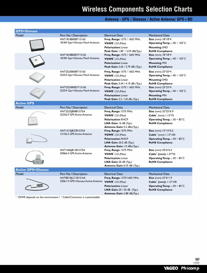
167
Wireless Components Selection ChartsAntenna - GPS / Glonass / Active Antenna/ GPS+BD
GPS+GlonassModel Part No./ Description Electrical Data Mechanical Data
ANT1818B00BT1516S 18184 Gps+Glonass Patch Antenna
Freq. Range: 1575 / 1602 MHz Size (mm): 18*18*4VSWR*: 2.0 (Max) Operating Temp. : -40 ~ 105°C
Polarization: Linear Mounting: SMDPeak Gain: 1.89 / 2.59 dBi(Typ.) RoHS Compliance
ANT1818B00DT1516S 18184 Gps+Glonass Patch Antenna
Freq. Range: 1575 / 1602 MHz Size (mm): 18*18*4VSWR*: 2.0 (Max) Operating Temp. : -40 ~ 105°C
Polarization: Linear Mounting: PINPeak Gain: 2.65 / 2.79 dBi (Typ.) RoHS Compliance
ANT2525B00BT1516S25254 Gps+Glonass Patch Antenna
Freq. Range: 1575 / 1602 MHz Size (mm): 25*25*4VSWR*: 2.0 (Max) Operating Temp. : -40 ~ 105°C
Polarization: Linear Mounting: SMDPeak Gain: 3.44 / 4.10 dBi (Typ.) RoHS Compliance
ANT2525B00DT1516S25254 Gps+Glonass Patch Antenna
Freq. Range: 1575 / 1602 MHz Size (mm): 25*25*4VSWR*: 2.0 (Max) Operating Temp. : -40 ~ 105°C
Polarization: Linear Mounting: PINPeak Gain: 3.5 / 3.8 dBi (Typ.) RoHS Compliance
Active GPSModel Part No./ Description Electrical Data Mechanical Data
ANT2525JB08B1575A 25256.9 GPS Active Antenna
Freq. Range: 1575 MHz Size (mm): 25*25*6.9VSWR*: 2.0 (Max) Cable* (mm): 1.13*75Polarization: RHCP Operating Temp. : -30 ~ 85°CLNA Gain: 16 dB (Typ.) RoHS ComplianceAntenna Gain: 5.5 dBic(Typ.)
ANT1515JB27B1575A 15156.5 GPS Active Antenna
Freq. Range: 1575 MHz Size (mm): 15*15*6.5VSWR*: 2.0 (Max) Cable* (mm): 1.13*100 Polarization: RHCP Operating Temp. : -30 ~ 85°CLNA Gain: 20.5 dB (Typ.) RoHS ComplianceAntenna Gain: 1.0 dBic(Typ.)
ANT1606JB12B1575A 20066.4 GPS Active Antenna
Freq. Range: 1575 MHz Size (mm): 20*6*6.4VSWR*: 2.0 (Max) Cable* (mm): 1.37*93 Polarization: Linear Operating Temp. : -30 ~ 85°CLNA Gain: 20 dB (Typ.) RoHS ComplianceAntenna Gain: 0.35 dBi (Typ.)
Active GPS+GlonassModel Part No./ Description Electrical Data Mechanical Data
ANT8010JLC1B1516A22061.9 GPS+Glonass Active Antenna
Freq. Range: 1575/1602 MHz Size (mm): 22*6*1.9VSWR*: 2.0 (Max) Cable* (mm): 1.13*100 Polarization: Linear Operating Temp. : -30 ~ 85°CLNA Gain: 20 / 20 dB (Typ.) RoHS ComplianceAntenna Gain: 5.88 dBi(Typ.)
* VSWR depends on the environment / * Cable/Connector is customizable
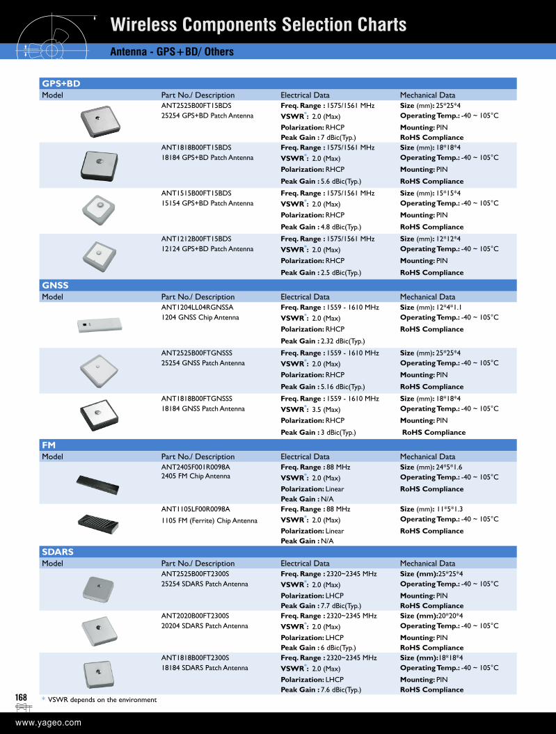
168
Wireless Components Selection ChartsAntenna - GPS+BD/ Others
GPS+BDModel Part No./ Description Electrical Data Mechanical Data
ANT2525B00FT15BDS Freq. Range : 1575/1561 MHz Size (mm): 25*25*425254 GPS+BD Patch Antenna VSWR*: 2.0 (Max) Operating Temp.: -40 ~ 105°C
Polarization: RHCP Mounting: PINPeak Gain : 7 dBic(Typ.) RoHS Compliance
ANT1818B00FT15BDS Freq. Range : 1575/1561 MHz Size (mm): 18*18*418184 GPS+BD Patch Antenna VSWR*: 2.0 (Max) Operating Temp.: -40 ~ 105°C
Polarization: RHCP Mounting: PIN
Peak Gain : 5.6 dBic(Typ.) RoHS Compliance
ANT1515B00FT15BDS Freq. Range : 1575/1561 MHz Size (mm): 15*15*415154 GPS+BD Patch Antenna VSWR*: 2.0 (Max) Operating Temp.: -40 ~ 105°C
Polarization: RHCP Mounting: PIN
Peak Gain : 4.8 dBic(Typ.) RoHS Compliance
ANT1212B00FT15BDS Freq. Range : 1575/1561 MHz Size (mm): 12*12*412124 GPS+BD Patch Antenna VSWR*: 2.0 (Max) Operating Temp.: -40 ~ 105°C
Polarization: RHCP Mounting: PIN
Peak Gain : 2.5 dBic(Typ.) RoHS Compliance
GNSSModel Part No./ Description Electrical Data Mechanical Data
ANT1204LL04RGNSSA Freq. Range : 1559 - 1610 MHz Size (mm): 12*4*1.11204 GNSS Chip Antenna VSWR*: 2.0 (Max) Operating Temp.: -40 ~ 105°C
Polarization: RHCP RoHS Compliance
Peak Gain : 2.32 dBic(Typ.)
ANT2525B00FTGNSSS Freq. Range : 1559 - 1610 MHz Size (mm): 25*25*425254 GNSS Patch Antenna VSWR*: 2.0 (Max) Operating Temp.: -40 ~ 105°C
Polarization: RHCP Mounting: PIN
Peak Gain : 5.16 dBic(Typ.) RoHS Compliance
ANT1818B00FTGNSSS Freq. Range : 1559 - 1610 MHz Size (mm): 18*18*418184 GNSS Patch Antenna VSWR*: 3.5 (Max) Operating Temp.: -40 ~ 105°C
Polarization: RHCP Mounting: PIN
Peak Gain : 3 dBic(Typ.) RoHS Compliance
FMModel Part No./ Description Electrical Data Mechanical Data
ANT2405F001R0098A 2405 FM Chip Antenna
Freq. Range : 88 MHz Size (mm): 24*5*1.6VSWR*: 2.0 (Max) Operating Temp.: -40 ~ 105°C
Polarization: Linear RoHS CompliancePeak Gain : N/A
ANT1105LF00R0098A
1105 FM (Ferrite) Chip Antenna
Freq. Range : 88 MHz Size (mm): 11*5*1.3VSWR*: 2.0 (Max) Operating Temp.: -40 ~ 105°C
Polarization: Linear RoHS CompliancePeak Gain : N/A
SDARSModel Part No./ Description Electrical Data Mechanical Data
ANT2525B00FT2300S Freq. Range : 2320~2345 MHz Size (mm):25*25*425254 SDARS Patch Antenna VSWR*: 2.0 (Max) Operating Temp.: -40 ~ 105°C
Polarization: LHCP Mounting: PINPeak Gain : 7.7 dBic(Typ.) RoHS Compliance
ANT2020B00FT2300S Freq. Range : 2320~2345 MHz Size (mm):20*20*420204 SDARS Patch Antenna VSWR*: 2.0 (Max) Operating Temp.: -40 ~ 105°C
Polarization: LHCP Mounting: PINPeak Gain : 6 dBic(Typ.) RoHS Compliance
ANT1818B00FT2300S Freq. Range : 2320~2345 MHz Size (mm):18*18*418184 SDARS Patch Antenna VSWR*: 2.0 (Max) Operating Temp.: -40 ~ 105°C
Polarization: LHCP Mounting: PINPeak Gain : 7.6 dBic(Typ.) RoHS Compliance
* VSWR depends on the environment
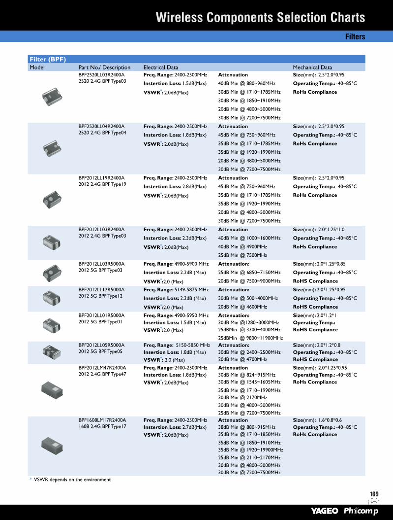
169
Wireless Components Selection ChartsFilters
Filter (BPF)Model Part No./ Description Electrical Data Mechanical Data
BPF2520LL03R2400A2520 2.4G BPF Type03
Freq. Range: 2400-2500MHz Attenuation Size(mm): 2.5*2.0*0.95
Instertion Loss: 1.5dB(Max) 40dB Min @ 880~960MHz Operating Temp.: -40~85°C
VSWR*: 2.0dB(Max) 30dB Min @ 1710~1785MHz RoHs Compliance
30dB Min @ 1850~1910MHz
20dB Min @ 4800~5000MHz
30dB Min @ 7200~7500MHz
BPF2520LL04R2400A2520 2.4G BPF Type04
Freq. Range: 2400-2500MHz Attenuation Size(mm): 2.5*2.0*0.95
Instertion Loss: 1.8dB(Max) 45dB Min @ 750~960MHz Operating Temp.: -40~85°C
VSWR*: 2.0dB(Max) 35dB Min @ 1710~1785MHz RoHs Compliance
35dB Min @ 1920~1990MHz
20dB Min @ 4800~5000MHz
30dB Min @ 7200~7500MHz
BPF2012LL19R2400A2012 2.4G BPF Type19
Freq. Range: 2400-2500MHz Attenuation Size(mm): 2.5*2.0*0.95
Instertion Loss: 2.8dB(Max) 45dB Min @ 750~960MHz Operating Temp.: -40~85°C
VSWR*: 2.0dB(Max) 35dB Min @ 1710~1785MHz RoHs Compliance
35dB Min @ 1920~1990MHz
20dB Min @ 4800~5000MHz
30dB Min @ 7200~7500MHz
BPF2012LL03R2400A2012 2.4G BPF Type03
Freq. Range: 2400-2500MHz Attenuation Size(mm): 2.0*1.25*1.0
Instertion Loss: 2.3dB(Max) 40dB Min @ 1000~1600MHz Operating Temp.: -40~85°C
VSWR*: 2.0dB(Max) 40dB Min @ 4900MHz RoHs Compliance
25dB Min @ 7500MHz
BPF2012LL03R5000A2012 5G BPF Type03
Freq. Range: 4900-5900 MHz Attenuation: Size(mm): 2.0*1.25*0.85
Insertion Loss: 2.2dB (Max) 25dB Min @ 6850~7150MHz Operating Temp.: -40~85°C
VSWR*:2.0 (Max) 20dB Min @ 7500~9000MHz RoHS Compliance
BPF2012LL12R5000A2012 5G BPF Type12
Freq. Range: 5149-5875 MHz Attenuation: Size(mm): 2.0*1.25*0.95
Insertion Loss: 2.2dB (Max) 30dB Min @ 500~4000MHz Operating Temp.: -40~85°C
VSWR*:2.0 (Max) 20dB Min @ 4600MHz RoHS Compliance
BPF2012LL01R5000A 2012 5G BPF Type01
Freq. Range: 4900-5950 MHz Attenuation: Size(mm): 2.0*1.2*1Insertion Loss: 1.5dB (Max) 30dB Min @1280~3000MHz Operating Temp.: VSWR*:2.0 (Max) 25dBMin @ 3300~4000MHz RoHS Compliance
25dBMin @ 9800~11900MHzBPF2012LL05R5000A 2012 5G BPF Type05
Freq. Range: 5150-5850 MHz Attenuation: Size(mm): 2.0*1.2*0.8Insertion Loss: 1.8dB (Max) 30dB Min @ 2400~2500MHz Operating Temp.: -40~85°CVSWR*: 2.0 (Max) 20dB Min @ 4700MHz RoHS Compliance
BPF2012LM47R2400A2012 2.4G BPF Type47
Freq. Range: 2400-2500MHz Attenuation Size(mm): 2.0*1.25*0.95Instertion Loss: 1.8dB(Max) 30dB Min @ 824~915MHz Operating Temp.: -40~85°CVSWR*: 2.0dB(Max) 30dB Min @ 1545~1605MHz RoHs Compliance
35dB Min @ 1710~1990MHz30dB Min @ 2170MHz30dB Min @ 4800~5000MHz25dB Min @ 7200~7500MHz
BPF1608LM17R2400A1608 2.4G BPF Type17
Freq. Range: 2400-2500MHz Attenuation Size(mm): 1.6*0.8*0.6Instertion Loss: 2.7dB(Max) 38dB Min @ 880~915MHz Operating Temp.: -40~85°CVSWR*: 2.0dB(Max) 35dB Min @ 1710~1850MHz RoHs Compliance
35dB Min @ 1850~1910MHz35dB Min @ 1920~19900MHz25dB Min @ 2110~2170MHz30dB Min @ 4800~5000MHz30dB Min @ 7200~7500MHz
* VSWR depends on the environment
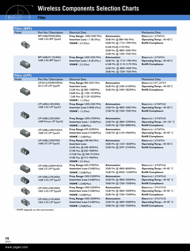
170
Wireless Components Selection ChartsFilter
Filter (BPF)Model Part No./ Description Electrical Data Mechanical Data
BPF1608LM02R2400A 1608 2.4G BPF Type02
Freq. Range: 2400-2500 MHz Attenuation: Size(mm): 1.6*0.8*0.6Insertion Loss: 1.7 dB (Max) 30dB Min @ 880~960 MHz Operating Temp.: -40~85°CVSWR*: 2.0 (Max) 20dB Min @ 1710~1990 MHz RoHS Compliance
8.5dB Min@ 2170 MHz20dB Min @ 4800~5000 MHz25dB Min @ 7200~7500 MHz
BPF1608LM11R2400A 1608 2.4G BPF Type11
Freq. Range: 2400-2500 MHz Attenuation: Size(mm): 1.6*0.8*0.6Insertion Loss: 1.8 dB (Max.) 20dB Min @ 1710~1990 MHz Operating Temp.: -40~85°CVSWR*: 2.0 (Max) 6.5dB Min @ 2110~2170 MHz RoHS Compliance
25dB Min @ 4800~5000 MHz20dB Min @ 7200~7500 MHz
Filter (LPF)Model Part No./ Description Electrical Data Mechanical Data
LPF2012LM59RWPENA2012 LTE LPF Type59
Freq. Range: 800-2025 MHz Attenuation Size(mm): 2.0*1.25*0.9Insertion Loss: 26dB Min @ 2300~6100MHz Operating Temp.: -40~85°C0.5dB Max @ 800~1000MHz 35dB Min @ 3400~3820MHz RoHS Compliance0.8dB Max @ 1700~1910MHz1.5dB Max @ 2120~2025MHzVSWR*: 1.5 (Max)
LPF1608LL53R2400A 1608 2.4G LPF Type53
Freq. Range: 2400-2500 MHz Attenuation: Size(mm): 1.6*0.8*0.65Insertion Loss: 0.48dB (Max) 35dB Min @ 4800~5000 MHz Operating Temp.: -40~85°CVSWR*: 1.5 (Max) 27dB Min @ 7200~7500 MHz RoHS Compliance
LPF1608LL52R2500A1608 Wimax LPF Type52
Freq. Range: 2300-2700MHz Attenuation: Size(mm): 1.6*0.8*0.65Instertion Loss: 1.25dB(Max) 35dB Min @ 4800~5390MHz Operating Temp.: -40~105 °CVSWR*: 1.5dB(Max) 25dB Min @ 7200~8085MHz RoHS Compliance
LPF1608LL54RWHEXA1608 LTE LPF Type54
Freq. Range: 699-2690MHz Attenuation: Size(mm): 1.6*0.8*0.6Instertion Loss: 0.25dB(Max) 23dB Min @ 5150~5960MHz Operating Temp.: -40~85 °C
VSWR*: 1.5dB(Max) RoHS Compliance
LPF1608LL55R0709A1608 LTE LPF Type55
Freq. Range: 698-960 MHz Attenuation Size(mm): 1.6*0.8*0.6Insertion Loss: 30dB Min @ 1554~1830MHz Operating Temp.: -40~85°C0.6dB Max @ 698~830MHz 35dB Min @ 2097~2745MHz RoHS Compliance0.7dB Max @ 830~900MHz0.75dB Max @ 900~915MHz0.9dB Max @ 915~960MHzVSWR*: 2.0 (Max)
LPF1608LL56RWHEXA1608 LTE LPF Type56
Freq. Range: 600-2700MHz Attenuation: Size(mm): 1.6*0.8*0.65Instertion Loss: 0.5dB(Max) 30dB Min @ 4800~8000MHz Operating Temp.: -40~85 °C
VSWR*: 2.0dB(Max) 25dB Min @ 8500~12500MHz RoHS Compliance
LPF1608LL57R2400A1608 2.4G LPF Type57
Freq. Range: 2400-2500MHz Attenuation: Size(mm): 1.6*0.8*0.65Instertion Loss: 0.6dB(Max) 35dB Min @ 4800~5000MHz Operating Temp.: -40~85 °C
VSWR*: 2.0dB(Max) 30dB Min @ 7200~7500MHz RoHS Compliance
LPF1005LL50R2400A1005 2.4G LPF Type50
Freq. Range: 2400-2500MHz Attenuation: Size(mm): 1.0*0.5*0.35Instertion Loss: 0.5dB(Max) 25dB Min @ 4800~5000MHz Operating Temp.: -40~85 °C
VSWR*: 2.0dB(Max) 20dB Min @ 7200~7500MHz RoHS Compliance
LPF1005LL51R2400A1005 2.4G LPF Type51
Freq. Range: 2400-2500MHz Attenuation: Size(mm): 1.0*0.5*0.35Instertion Loss: 0.5dB(Max) 25dB Min @ 4800~5000MHz Operating Temp.: -40~85 °C
VSWR*: 2.0dB(Max) 20dB Min @ 7200~7500MHz RoHS Compliance
* VSWR depends on the environment
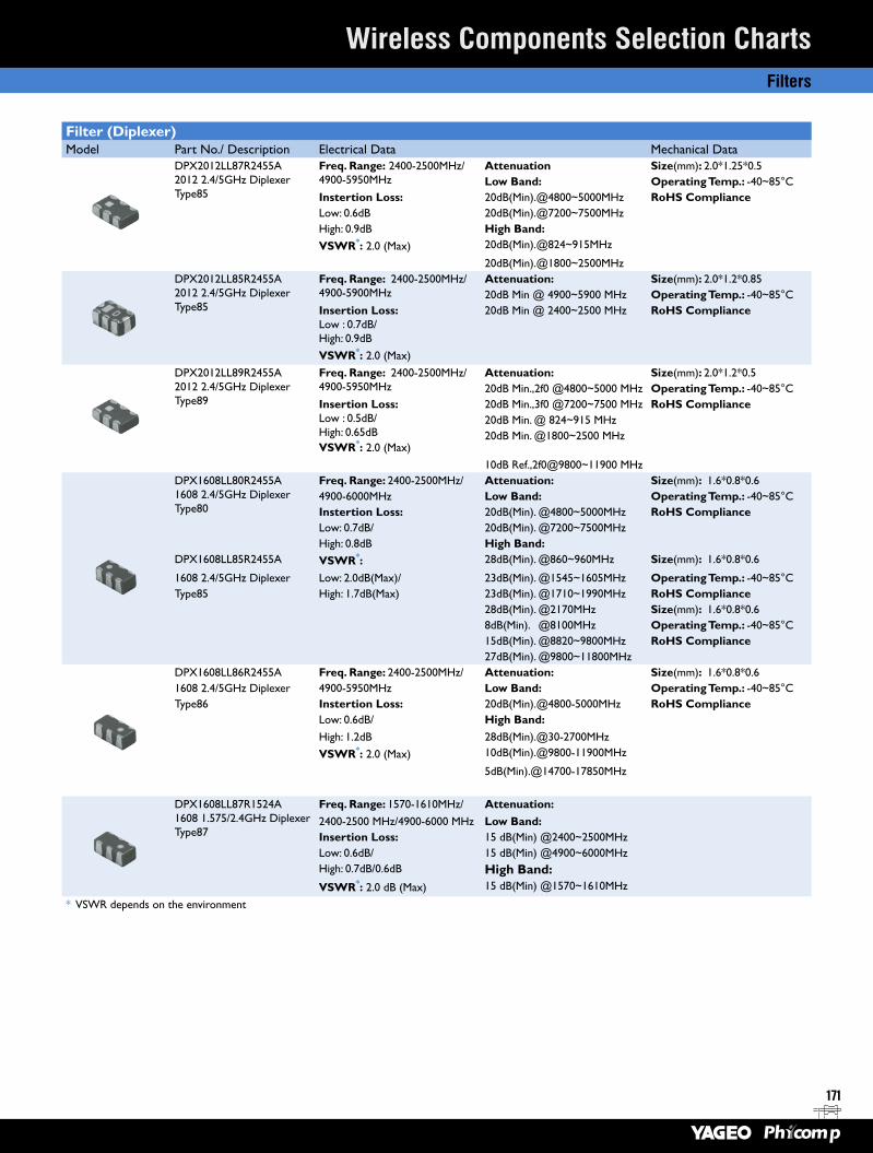
171
Wireless Components Selection ChartsFilters
Filter (Diplexer)Model Part No./ Description Electrical Data Mechanical Data
DPX2012LL87R2455A2012 2.4/5GHz Diplexer Type85
Freq. Range: 2400-2500MHz/4900-5950MHz
Attenuation Size(mm): 2.0*1.25*0.5Low Band: Operating Temp.: -40~85°C
Instertion Loss: 20dB(Min).@4800~5000MHz RoHS ComplianceLow: 0.6dB 20dB(Min).@7200~7500MHzHigh: 0.9dB High Band:VSWR*: 2.0 (Max) 20dB(Min).@824~915MHz
20dB(Min).@1800~2500MHzDPX2012LL85R2455A 2012 2.4/5GHz Diplexer Type85
Freq. Range: 2400-2500MHz/ 4900-5900MHz
Attenuation: Size(mm): 2.0*1.2*0.8520dB Min @ 4900~5900 MHz Operating Temp.: -40~85°C
Insertion Loss: Low : 0.7dB/ High: 0.9dB
20dB Min @ 2400~2500 MHz RoHS Compliance
VSWR*: 2.0 (Max)DPX2012LL89R2455A 2012 2.4/5GHz Diplexer Type89
Freq. Range: 2400-2500MHz/ 4900-5950MHz
Attenuation: Size(mm): 2.0*1.2*0.520dB Min.,2f0 @4800~5000 MHz Operating Temp.: -40~85°C
Insertion Loss: Low : 0.5dB/ High: 0.65dBVSWR*: 2.0 (Max)
20dB Min.,3f0 @7200~7500 MHz RoHS Compliance20dB Min. @ 824~915 MHz20dB Min. @1800~2500 MHz
10dB Ref.,2f0@9800~11900 MHzDPX1608LL80R2455A1608 2.4/5GHz Diplexer Type80
Freq. Range: 2400-2500MHz/ Attenuation: Size(mm): 1.6*0.8*0.64900-6000MHz Low Band: Operating Temp.: -40~85°CInstertion Loss: 20dB(Min). @4800~5000MHz RoHS ComplianceLow: 0.7dB/ 20dB(Min). @7200~7500MHzHigh: 0.8dB High Band:
DPX1608LL85R2455A VSWR*: 28dB(Min). @860~960MHz Size(mm): 1.6*0.8*0.6
1608 2.4/5GHz Diplexer Low: 2.0dB(Max)/ 23dB(Min). @1545~1605MHz Operating Temp.: -40~85°CType85 High: 1.7dB(Max) 23dB(Min). @1710~1990MHz RoHS Compliance
28dB(Min). @2170MHz Size(mm): 1.6*0.8*0.68dB(Min). @8100MHz Operating Temp.: -40~85°C15dB(Min). @8820~9800MHz RoHS Compliance27dB(Min). @9800~11800MHz
DPX1608LL86R2455A Freq. Range: 2400-2500MHz/ Attenuation: Size(mm): 1.6*0.8*0.61608 2.4/5GHz Diplexer 4900-5950MHz Low Band: Operating Temp.: -40~85°CType86 Instertion Loss: 20dB(Min).@4800-5000MHz RoHS Compliance
Low: 0.6dB/ High Band:High: 1.2dB 28dB(Min).@30-2700MHzVSWR*: 2.0 (Max) 10dB(Min).@9800-11900MHz
5dB(Min).@14700-17850MHz
DPX1608LL87R1524A1608 1.575/2.4GHz Diplexer Type87
Freq. Range: 1570-1610MHz/ Attenuation:2400-2500 MHz/4900-6000 MHz Low Band:Insertion Loss: 15 dB(Min) @2400~2500MHzLow: 0.6dB/ 15 dB(Min) @4900~6000MHzHigh: 0.7dB/0.6dB High Band:VSWR*: 2.0 dB (Max) 15 dB(Min) @1570~1610MHz
* VSWR depends on the environment
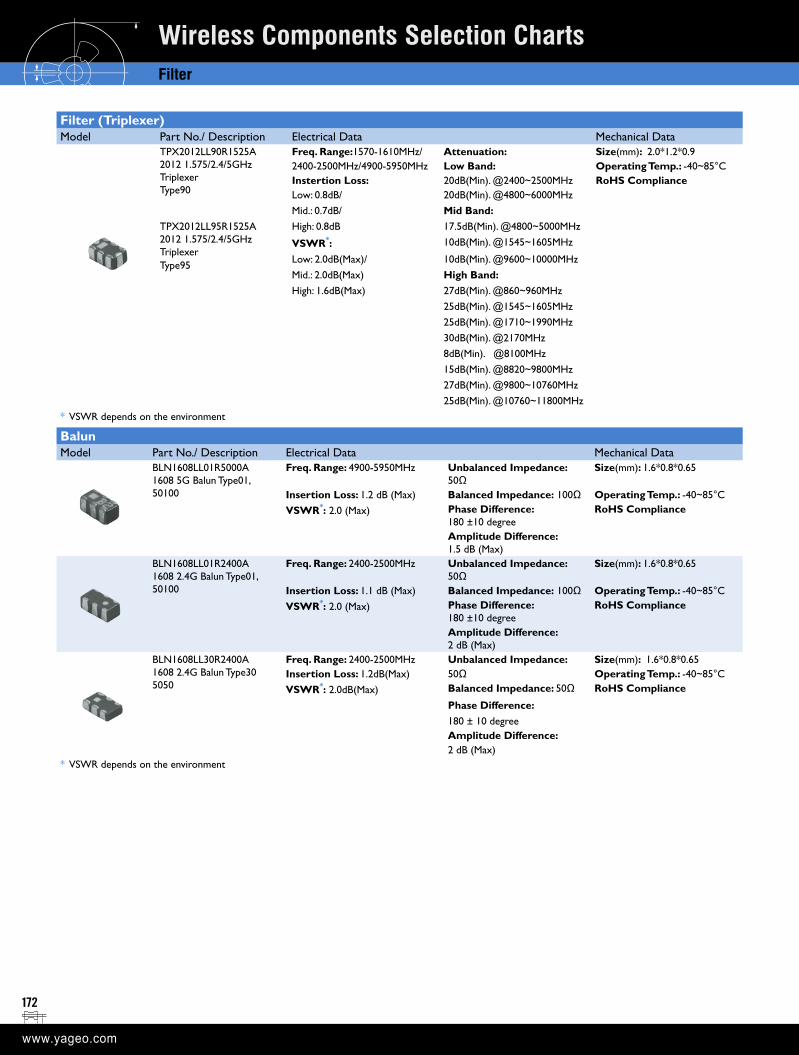
172
Filter (Triplexer)Model Part No./ Description Electrical Data Mechanical Data
TPX2012LL90R1525A2012 1.575/2.4/5GHz TriplexerType90
Freq. Range:1570-1610MHz/ Attenuation: Size(mm): 2.0*1.2*0.92400-2500MHz/4900-5950MHz Low Band: Operating Temp.: -40~85°CInstertion Loss: 20dB(Min). @2400~2500MHz RoHS ComplianceLow: 0.8dB/ 20dB(Min). @4800~6000MHzMid.: 0.7dB/ Mid Band:
TPX2012LL95R1525A2012 1.575/2.4/5GHz TriplexerType95
High: 0.8dB 17.5dB(Min). @4800~5000MHz
VSWR*: 10dB(Min). @1545~1605MHz
Low: 2.0dB(Max)/ 10dB(Min). @9600~10000MHzMid.: 2.0dB(Max) High Band:High: 1.6dB(Max) 27dB(Min). @860~960MHz
25dB(Min). @1545~1605MHz25dB(Min). @1710~1990MHz30dB(Min). @2170MHz8dB(Min). @8100MHz15dB(Min). @8820~9800MHz27dB(Min). @9800~10760MHz25dB(Min). @10760~11800MHz
* VSWR depends on the environment
BalunModel Part No./ Description Electrical Data Mechanical Data
BLN1608LL01R5000A1608 5G Balun Type01, 50100
Freq. Range: 4900-5950MHz Unbalanced Impedance: 50Ω
Size(mm): 1.6*0.8*0.65
Insertion Loss: 1.2 dB (Max) Balanced Impedance: 100Ω Operating Temp.: -40~85°CVSWR*: 2.0 (Max) Phase Difference:
180 ±10 degreeRoHS Compliance
Amplitude Difference: 1.5 dB (Max)
BLN1608LL01R2400A1608 2.4G Balun Type01, 50100
Freq. Range: 2400-2500MHz Unbalanced Impedance: 50Ω
Size(mm): 1.6*0.8*0.65
Insertion Loss: 1.1 dB (Max) Balanced Impedance: 100Ω Operating Temp.: -40~85°CVSWR*: 2.0 (Max) Phase Difference:
180 ±10 degreeRoHS Compliance
Amplitude Difference: 2 dB (Max)
BLN1608LL30R2400A1608 2.4G Balun Type30 5050
Freq. Range: 2400-2500MHz Unbalanced Impedance: Size(mm): 1.6*0.8*0.65Insertion Loss: 1.2dB(Max) 50Ω Operating Temp.: -40~85°CVSWR*: 2.0dB(Max) Balanced Impedance: 50Ω RoHS Compliance
Phase Difference: 180 ± 10 degreeAmplitude Difference: 2 dB (Max)
* VSWR depends on the environment
Wireless Components Selection ChartsFilter
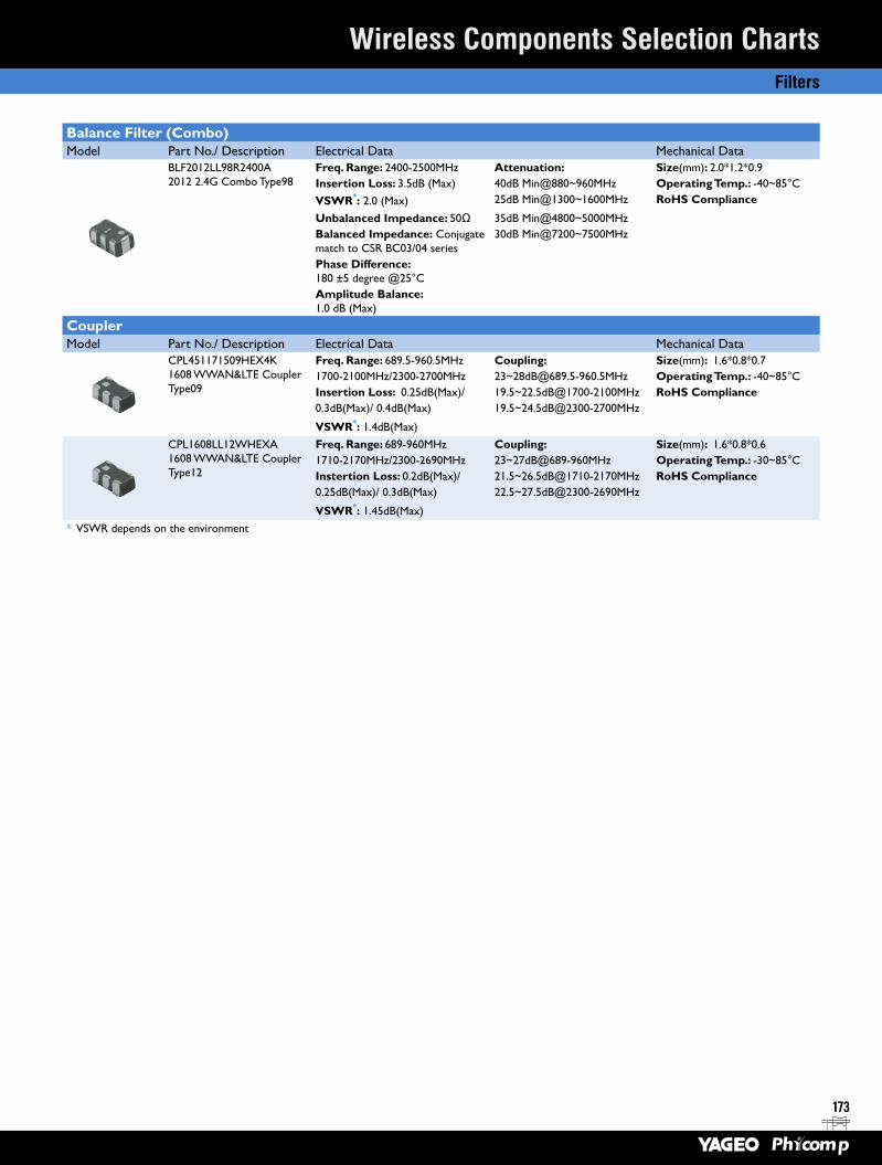
173
Balance Filter (Combo)Model Part No./ Description Electrical Data Mechanical Data
BLF2012LL98R2400A2012 2.4G Combo Type98
Freq. Range: 2400-2500MHz Attenuation: Size(mm): 2.0*1.2*0.9Insertion Loss: 3.5dB (Max) 40dB Min@880~960MHz Operating Temp.: -40~85°CVSWR*: 2.0 (Max) 25dB Min@1300~1600MHz RoHS Compliance
Unbalanced Impedance: 50Ω 35dB Min@4800~5000MHzBalanced Impedance: Conjugate match to CSR BC03/04 series
30dB Min@7200~7500MHz
Phase Difference: 180 ±5 degree @25°CAmplitude Balance: 1.0 dB (Max)
CouplerModel Part No./ Description Electrical Data Mechanical Data
CPL451171509HEX4K1608 WWAN<E CouplerType09
Freq. Range: 689.5-960.5MHz Coupling: Size(mm): 1.6*0.8*0.71700-2100MHz/2300-2700MHz [email protected] Operating Temp.: -40~85°CInsertion Loss: 0.25dB(Max)/ 19.5~22.5dB@1700-2100MHz RoHS Compliance0.3dB(Max)/ 0.4dB(Max) 19.5~24.5dB@2300-2700MHz
VSWR*: 1.4dB(Max)CPL1608LL12WHEXA1608 WWAN<E CouplerType12
Freq. Range: 689-960MHz Coupling: Size(mm): 1.6*0.8*0.61710-2170MHz/2300-2690MHz 23~27dB@689-960MHz Operating Temp.: -30~85°CInstertion Loss: 0.2dB(Max)/ 21.5~26.5dB@1710-2170MHz RoHS Compliance0.25dB(Max)/ 0.3dB(Max) 22.5~27.5dB@2300-2690MHz
VSWR*: 1.45dB(Max)* VSWR depends on the environment
Wireless Components Selection ChartsFilters
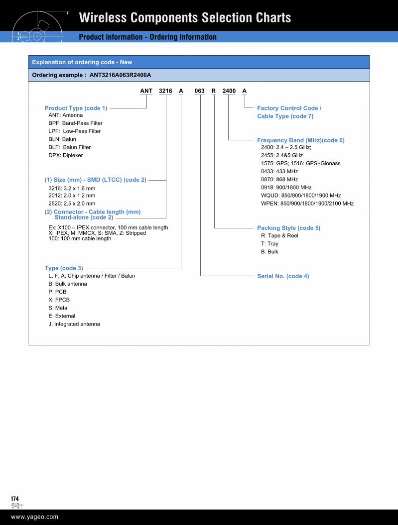
174
Wireless Components Selection ChartsProduct information - Ordering Information
Explanation of ordering code - New
Ordering example : ANT3216A063R2400A
ANT 3216 A 063 R 2400 A
Product Type (code 1) Factory Control Code / ANT: Antenna Cable Type (code 7)BPF: Band-Pass Filter LPF: Low-Pass FilterBLN: Balun Frequency Band (MHz)(code 6)BLF: Balun Filter 2400: 2.4 – 2.5 GHz; DPX: Diplexer 2455: 2.4&5 GHz
1575: GPS; 1516: GPS+Glonass0433: 433 MHz
(1) Size (mm) - SMD (LTCC) (code 2) 0870: 868 MHz3216: 3.2 x 1.6 mm 0918: 900/1800 MHz2012: 2.0 x 1.2 mm WQUD: 850/900/1800/1900 MHz2520: 2.5 x 2.0 mm WPEN: 850/900/1800/1900/2100 MHz
(2) Connector - Cable length (mm) Stand-alone (code 2)
Ex: X100 – IPEX connector, 100 mm cable lengthX: IPEX, M: MMCX, S: SMA, Z: Stripped100: 100 mm cable length
Packing Style (code 5)R: Tape & ReelT: TrayB: Bulk
Type (code 3)L, F, A: Chip antenna / Filter / Balun Serial No. (code 4)B: Bulk antennaP: PCBX: FPCBS: MetalE: ExternalJ: Integrated antenna
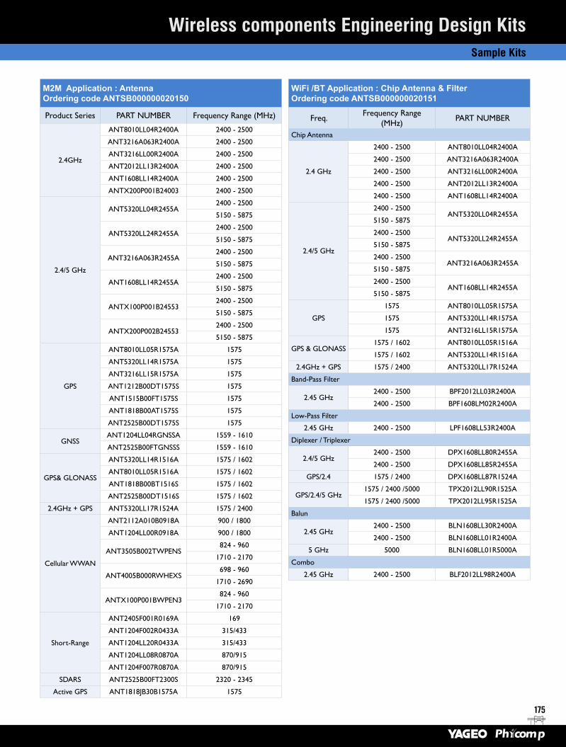
175
Wireless components Engineering Design KitsSample Kits
M2M Application : AntennaOrdering code ANTSB000000020150
Product Series PART NUMBER Frequency Range (MHz)
2.4GHz
ANT8010LL04R2400A 2400 - 2500
ANT3216A063R2400A 2400 - 2500
ANT3216LL00R2400A 2400 - 2500
ANT2012LL13R2400A 2400 - 2500
ANT1608LL14R2400A 2400 - 2500
ANTX200P001B24003 2400 - 2500
2.4/5 GHz
ANT5320LL04R2455A2400 - 2500
5150 - 5875
ANT5320LL24R2455A2400 - 2500
5150 - 5875
ANT3216A063R2455A2400 - 2500
5150 - 5875
ANT1608LL14R2455A2400 - 2500
5150 - 5875
ANTX100P001B245532400 - 2500
5150 - 5875
ANTX200P002B245532400 - 2500
5150 - 5875
GPS
ANT8010LL05R1575A 1575
ANT5320LL14R1575A 1575
ANT3216LL15R1575A 1575
ANT1212B00DT1575S 1575
ANT1515B00FT1575S 1575
ANT1818B00AT1575S 1575
ANT2525B00DT1575S 1575
GNSSANT1204LL04RGNSSA 1559 - 1610
ANT2525B00FTGNSSS 1559 - 1610
GPS& GLONASS
ANT5320LL14R1516A 1575 / 1602
ANT8010LL05R1516A 1575 / 1602
ANT1818B00BT1516S 1575 / 1602
ANT2525B00DT1516S 1575 / 1602
2.4GHz + GPS ANT5320LL17R1524A 1575 / 2400
Cellular WWAN
ANT2112A010B0918A 900 / 1800
ANT1204LL00R0918A 900 / 1800
ANT3505B002TWPENS824 - 960
1710 - 2170
ANT4005B000RWHEXS698 - 960
1710 - 2690
ANTX100P001BWPEN3824 - 960
1710 - 2170
Short-Range
ANT2405F001R0169A 169
ANT1204F002R0433A 315/433
ANT1204LL20R0433A 315/433
ANT1204LL08R0870A 870/915
ANT1204F007R0870A 870/915
SDARS ANT2525B00FT2300S 2320 - 2345
Active GPS ANT1818JB30B1575A 1575
WiFi /BT Application : Chip Antenna & Filter Ordering code ANTSB000000020151
Freq.Frequency Range
(MHz)PART NUMBER
Chip Antenna
2.4 GHz
2400 - 2500 ANT8010LL04R2400A
2400 - 2500 ANT3216A063R2400A
2400 - 2500 ANT3216LL00R2400A
2400 - 2500 ANT2012LL13R2400A
2400 - 2500 ANT1608LL14R2400A
2.4/5 GHz
2400 - 2500ANT5320LL04R2455A
5150 - 5875
2400 - 2500ANT5320LL24R2455A
5150 - 5875
2400 - 2500ANT3216A063R2455A
5150 - 5875
2400 - 2500ANT1608LL14R2455A
5150 - 5875
GPS
1575 ANT8010LL05R1575A
1575 ANT5320LL14R1575A
1575 ANT3216LL15R1575A
GPS & GLONASS1575 / 1602 ANT8010LL05R1516A
1575 / 1602 ANT5320LL14R1516A
2.4GHz + GPS 1575 / 2400 ANT5320LL17R1524A
Band-Pass Filter
2.45 GHz2400 - 2500 BPF2012LL03R2400A
2400 - 2500 BPF1608LM02R2400A
Low-Pass Filter
2.45 GHz 2400 - 2500 LPF1608LL53R2400A
Diplexer / Triplexer
2.4/5 GHz2400 - 2500 DPX1608LL80R2455A
2400 - 2500 DPX1608LL85R2455A
GPS/2.4 1575 / 2400 DPX1608LL87R1524A
GPS/2.4/5 GHz1575 / 2400 /5000 TPX2012LL90R1525A
1575 / 2400 /5000 TPX2012LL95R1525A
Balun
2.45 GHz2400 - 2500 BLN1608LL30R2400A
2400 - 2500 BLN1608LL01R2400A
5 GHz 5000 BLN1608LL01R5000A
Combo
2.45 GHz 2400 - 2500 BLF2012LL98R2400A

MULTILAYER CHIP VARISTORS
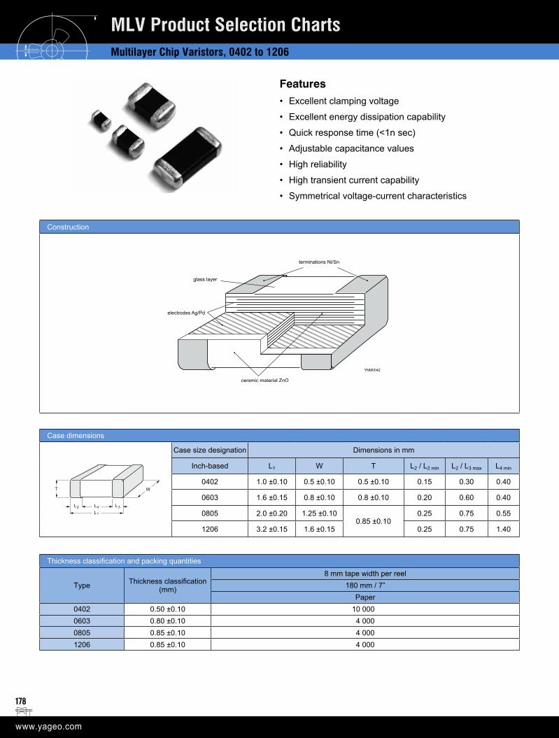
178
Case dimensions
T
L4
L1
L2 L3
W
Case size designation Dimensions in mm
Inch-based L1 W T L2 / L2 min L2 / L3 max L4 min
0402 1.0 ±0.10 0.5 ±0.10 0.5 ±0.10 0.15 0.30 0.40
0603 1.6 ±0.15 0.8 ±0.10 0.8 ±0.10 0.20 0.60 0.40
0805 2.0 ±0.20 1.25 ±0.100.85 ±0.10
0.25 0.75 0.55
1206 3.2 ±0.15 1.6 ±0.15 0.25 0.75 1.40
MLV Product Selection ChartsMultilayer Chip Varistors, 0402 to 1206
Construction
Features• Excellent clamping voltage
• Excellent energy dissipation capability
• Quick response time (<1n sec)
• Adjustable capacitance values
• High reliability
• High transient current capability
• Symmetrical voltage-current characteristics
Thickness classification and packing quantities
Type Thickness classification (mm)
8 mm tape width per reel180 mm / 7”
Paper0402 0.50 ±0.10 10 0000603 0.80 ±0.10 4 0000805 0.85 ±0.10 4 0001206 0.85 ±0.10 4 000
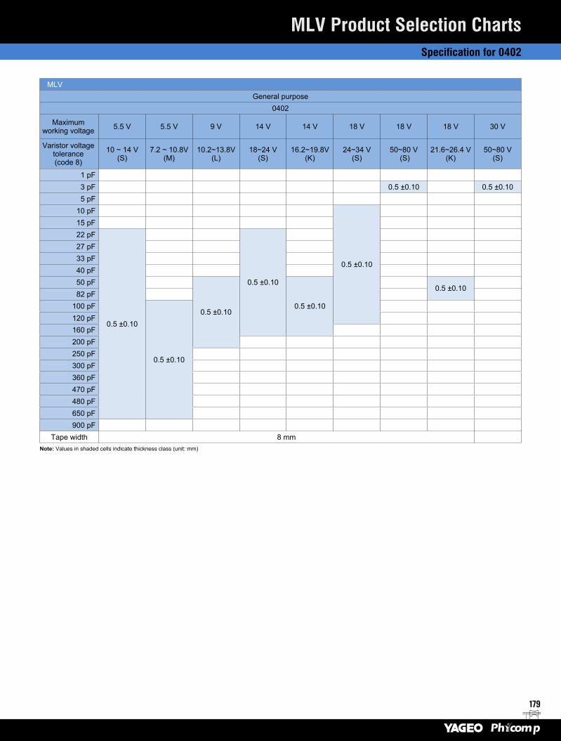
179
MLVGeneral purpose
0402
Maximum working voltage 5.5 V 5.5 V 9 V 14 V 14 V 18 V 18 V 18 V 30 V
Varistor voltagetolerance (code 8)
10 ~ 14 V (S)
7.2 ~ 10.8V (M)
10.2~13.8V (L)
18~24 V (S)
16.2~19.8V (K)
24~34 V (S)
50~80 V (S)
21.6~26.4 V (K)
50~80 V (S)
1 pF3 pF 0.5 ±0.10 0.5 ±0.105 pF
10 pF
0.5 ±0.10
15 pF22 pF
0.5 ±0.10
0.5 ±0.10
27 pF33 pF40 pF50 pF
0.5 ±0.100.5 ±0.10
0.5 ±0.1082 pF
100 pF
0.5 ±0.10
120 pF160 pF200 pF250 pF300 pF360 pF470 pF480 pF650 pF900 pF
Tape width 8 mmNote: Values in shaded cells indicate thickness class (unit: mm)
MLV Product Selection ChartsSpecification for 0402
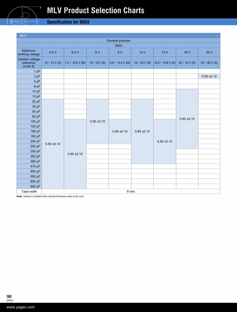
180
MLV Product Selection ChartsSpecification for 0603
MLVGeneral purpose
0603Maximum
working voltage 5.5 V 5.5 V 9 V 9 V 14 V 14 V 18 V 30 V
Varistor voltagetolerance (code 8)
10 ~ 14 V (S) 7.2 ~ 10.8 V (M) 14~ 18 V (S) 9.6 ~ 14.4 V (M) 18 ~ 24 V (S) 16.2 ~ 19.8 V (K) 24 ~ 32 V (S) 50 ~ 80 V (S)
1 pF3 pF 0.80 ±0.105 pF9 pF
10 pF
0.80 ±0.10
15 pF22 pF
0.80 ±0.10
0.80 ±0.10
0.80 ±0.10
33 pF50 pF82 pF
100 pF
0.80 ±0.10
0.80 ±0.10
0.80 ±0.10
120 pF160 pF180 pF200 pF250 pF300 pF350 pF360 pF470 pF650 pF680 pF800 pF900 pF
Tape width 8 mmNote: Values in shaded cells indicate thickness class (unit: mm)
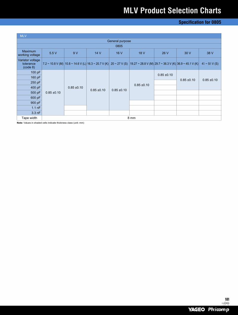
181
MLV Product Selection ChartsSpecification for 0805
MLVGeneral purpose
0805Maximum
working voltage 5.5 V 9 V 14 V 16 V 18 V 26 V 30 V 38 V
Varistor voltagetolerance (code 8)
7.2 ~ 10.8 V (M) 10.8 ~ 14.6 V (L) 16.3 ~ 20.7 V (K) 20 ~ 27 V (S) 19.27 ~ 28.8 V (M) 29.7 ~ 36.3 V (K) 36.9 ~ 45.1 V (K) 45 ~ 58 V (S)
100 pF
0.85 ±0.100.85 ±0.10
0.85 ±0.10 0.85 ±0.100.85 ±0.10
0.85 ±0.100.85 ±0.10 0.85 ±0.10
160 pF250 pF400 pF500 pF600 pF900 pF1.1 nF3.3 nF
Tape width 8 mmNote: Values in shaded cells indicate thickness class (unit: mm)
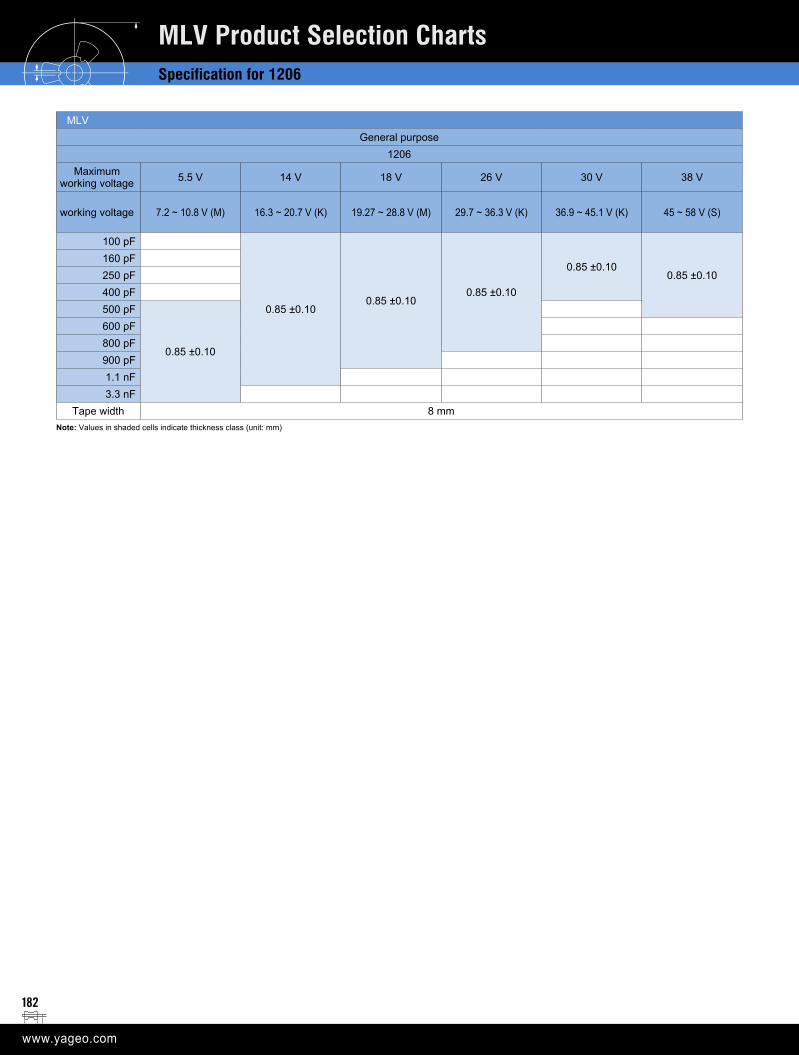
182
MLV Product Selection ChartsSpecification for 1206
MLVGeneral purpose
1206Maximum
working voltage 5.5 V 14 V 18 V 26 V 30 V 38 V
working voltage 7.2 ~ 10.8 V (M) 16.3 ~ 20.7 V (K) 19.27 ~ 28.8 V (M) 29.7 ~ 36.3 V (K) 36.9 ~ 45.1 V (K) 45 ~ 58 V (S)
100 pF
0.85 ±0.100.85 ±0.10
0.85 ±0.10
0.85 ±0.100.85 ±0.10
160 pF250 pF400 pF500 pF
0.85 ±0.10
600 pF800 pF900 pF1.1 nF3.3 nF
Tape width 8 mmNote: Values in shaded cells indicate thickness class (unit: mm)
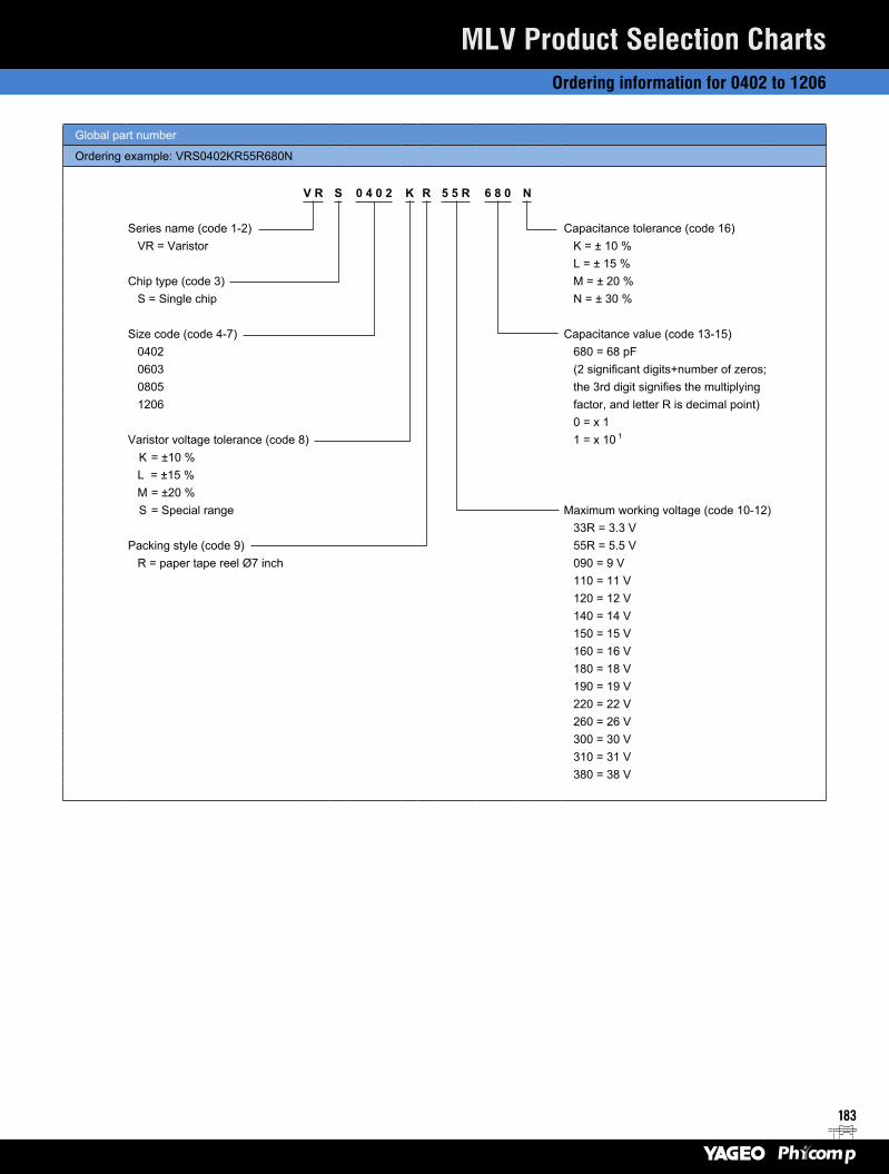
183
Global part number
Ordering example: VRS0402KR55R680N
V R S 0 4 0 2 K R 5 5 R 6 8 0 N
Series name (code 1-2) Capacitance tolerance (code 16)VR = Varistor K = ± 10 %
L = ± 15 %Chip type (code 3) M = ± 20 %
S = Single chip N = ± 30 %
Size code (code 4-7) Capacitance value (code 13-15)0402 680 = 68 pF0603 (2 significant digits+number of zeros; 0805 the 3rd digit signifies the multiplying 1206 factor, and letter R is decimal point)
0 = x 1Varistor voltage tolerance (code 8) 1 = x 10 1
K = ±10 %L = ±15 %M = ±20 % S = Special range Maximum working voltage (code 10-12) 33R = 3.3 V
Packing style (code 9) 55R = 5.5 VR = paper tape reel Ø7 inch 090 = 9 V
110 = 11 V120 = 12 V 140 = 14 V150 = 15 V160 = 16 V180 = 18 V190 = 19 V220 = 22 V260 = 26 V300 = 30 V310 = 31 V380 = 38 V
MLV Product Selection ChartsOrdering information for 0402 to 1206


Note:

Note:

Date of release: April 2017Printed in Taiwan
© YAGEO Corporation
All rights are reserved. Reproduction in whole or in part is prohibited without the prior written consent of the copyright owner.The information presented in this document does not form part of any quotation or contract, is believed to be accurate and reliable and may be changed without notice.
No liability will be accepted by the publisher for any consequence of its use. Publication thereof does not convey nor imply any license under patent or other industrial or intellectual property rights.
For a complete listing of all Yageo sales offices, distributors, and representatives, please visit "contact us" at
www.yageo.com
YAGEO - A GLOBAL COMPANY
ASIA
Suzhou, ChinaTel. +86 512 6825 5568Fax. +86 512 6825 5386
Shanghai, ChinaTel. +86 21 64858697
Dongguan, ChinaTel. +86 769 8772 0275Fax. +86 769 8791 0053
Shenzhen, ChinaTel. +86 755 8652 3739
Kuala Lumpur, MalaysiaTel. +60 3 8063 8864Fax. +60 3 8063 7376
Penang, MalaysiaTel. +60 4 3973049Fax. +60 4 3973050
Taipei, TaiwanTel. +886 2 6629 9999Fax. +886 2 6628 8886
EUROPE
Munich, GermanyTel. +49 8990 7784 380Fax. +49 8990 7784 379
Milan, ItalyTel. +39 02 6129 1017Fax. +39 02 6601 7490
Roermond, BeneluxTel. +31 475 385 555Fax. +31 475 385 589
Szombathely, HungaryTel. +36 94 517 702Fax. +36 94 517 701
Moscow, Russian FederationTel. +7 965 408 18 11Fax. +7 498 610 07 07
NORTH AMERICA
San Jose, U.S.A.Tel. +1 408 240 6200Fax. +1 408 240 6201
MexicoTel. +52 33 31330631Fax. +1 408 240 6201
Tokyo, JapanTel. +81 3 6809 3972Fax. +81 3 6809 3982
Seongnam, KoreaTel. +82 31 712 4797Fax. +82 31 712 5866
SingaporeTel. +65 6244 7800Fax. +65 6244 4943