Embed Size (px)
Citation preview
Joseph A. Floreano Rochester Convention Center Rochester, New York, United States
13 - 15 October 2015
Optifab, organized jointly by SPIE and APOMA, is the largest optical manufacturing conference and exhibition held in the United States.
optics.org product focus SPIE OPTIFAB 2015 Edition
product focus
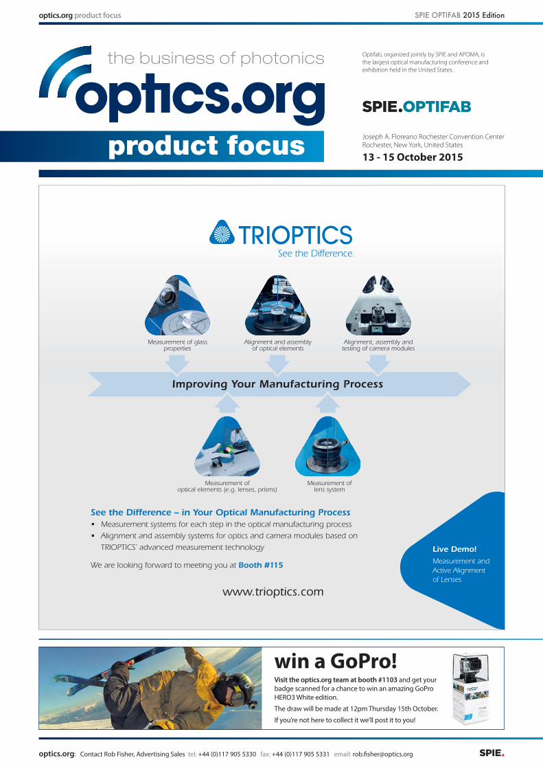
Measurement of lens system
Alignment, assembly and testing of camera modules
Measurement of optical elements (e.g. lenses, prisms)
Measurement of glass properties
Improving Your Manufacturing Process
Alignment and assembly of optical elements
See the Difference – in Your Optical Manufacturing Process • Measurement systems for each step in the optical manufacturing process
• Alignment and assembly systems for optics and camera modules based on
TRIOPTICS’ advanced measurement technology
We are looking forward to meeting you at Booth #115
Live Demo!Measurement and Active Alignment of Lenses
www.trioptics.com
optics.org: Contact Rob Fisher, Advertising Sales tel: +44 (0)117 905 5330 fax: +44 (0)117 905 5331 email: [email protected]
win a GoPro! Visit the optics.org team at booth #1103 and get your badge scanned for a chance to win an amazing GoPro HERO3 White edition.
The draw will be made at 12pm Thursday 15th October.
If you’re not here to collect it we’ll post it to you!
optics.org product focus SPIE OPTIFAB 2015 Edition2
optics.org: Contact Rob Fisher, Advertising Sales tel: +44 (0)117 905 5330 fax: +44 (0)117 905 5331 email: [email protected]
Aspheric andfree form optics
3D non-contactoptical pro�ler
FIND US SPIE optifab | booth 106
apexPLu
www.sensofar.com/pluapex
C
M
Y
CM
MY
CY
CMY
K
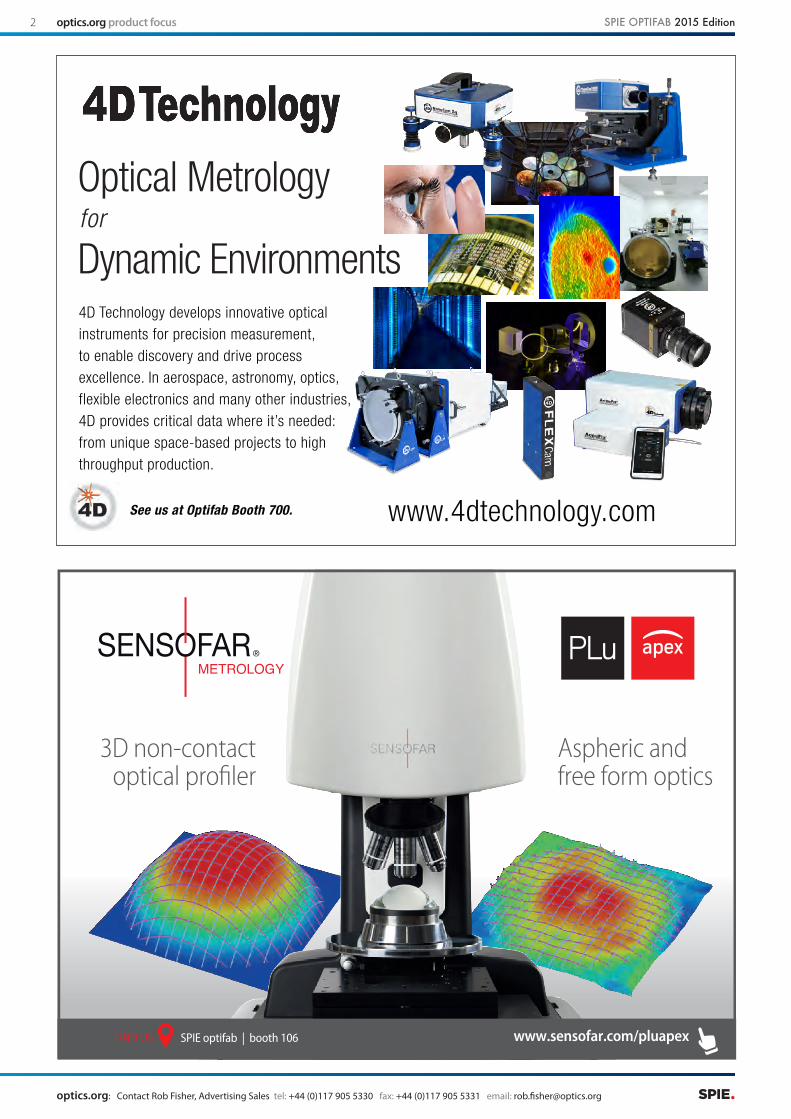
Optical Metrology
See us at Optifab Booth 700.
Dynamic Environmentsfor
4D Technology develops innovative optical instruments for precision measurement,to enable discovery and drive process excellence. In aerospace, astronomy, optics, flexible electronics and many other industries, 4D provides critical data where it’s needed: from unique space-based projects to high throughput production.
www.4dtechnology.com
optics.org product focus SPIE OPTIFAB 2015 Edition 3
optics.org: Contact Rob Fisher, Advertising Sales tel: +44 (0)117 905 5330 fax: +44 (0)117 905 5331 email: [email protected]
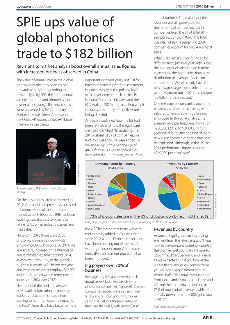
The value of annual sales in the global photonics market has been revised upwards to $182bn, according to new analysis by SPIE, the international society for optics and photonics (and owner of optics.org). The new results were presented by SPIE’s Industry and Market Strategist Steve Anderson at the Optics+Photonics expo exhibitors’ meeting in San Diego.
Revisions to market analysis boost overall annual sales figures, with increased business observed in China.
SPIE ups value of global photonics trade to $182 billion
On the basis of research performed to 2012, Anderson had previously assessed the annual value of the photonics market to be $160bn but SPIE has been working over the past two years to refine its list of key industry players and their sales.
He said, “In 2012 there were 2700 photonics companies worldwide, employing 686,000 people. By 2014, we saw an 18% increase in the number of active companies, now totaling 3194, sales were up by 15%, so the global business is worth $182 billion per year, and we now believe it employs 863,000 individuals, which would represent an increase of 26% over 2012.”
He described the updated analysis as “valuable information for industry leaders and academic researchers seeking to communicate the impact of the field.” These data have become more
important in recent years, not just for forecasting and supporting investment, but increasingly at the political level with developments such as the US National Photonics Initiative and the EC’s Horizon 2020 programs, into which serious state money and policies are being directed.
Anderson explained how the list had been refined and how the significant changes identified: ”In updating the 2012 dataset of 2713 companies, we took 193 out and 674 were added so we ended up with a net change of 481. Of these, 305 Asian companies were added, 91 European, and 81 from
Steve Anderson, SPIE’s Industry and Market Strategist.
Phot
o: M
atth
ew P
each
.
the US. The reason that there was a lot more activity added in Asia was that, since 2012, a lot of Chinese companies have been coming out of their shells, wanting to export more. At the same time, SPIE’s assessment procedure has been improved.”
Big players own 70% of businessInvestigating the data reveals much about recent business trends with photonics companies: “Since 2012, most companies added were in the under-$10m and $10m-to-$50m turnover categories. About three-quarters of firms are still SMEs, with under $10m
Geography of global components production, according to SPIE’s 2014 analysis.
Gra
phic
: S. A
nder
son
/ SPI
E.
annual business. The majority of the revenues are still generated from the minority of companies: just 63 companies from the 3194 total 2014 sample account for 70% of the total business while the remaining 2384 companies account for only 4% of total sales.”
What SPIE’s latest survey found to be different from just two years ago is that the industry’s job distribution is more even across the companies than is the distribution of revenues. Anderson commented, “We still clearly have the bias towards larger companies in terms of employment but in 2014 the picture is a little more spread out.”
One measure of companies’ operating efficiency and performance is the sales ratio, measurable in dollars per employee. In the 2014 analysis, the average yield per head was down from $230,000 (2012) to $211,000. “This is accounted for by the addition of many new Asian companies to the database,” he explained. “Although, in the US the 2014 performance figure is around $260,000 per employee.”
Revenues by countryAnderson highlighted an interesting element from the latest analysis. “If you look at the company count by country, the top five host countries are ranked: US, China, Japan, Germany and France, as we expected. But if you look at the where the revenues are coming from, you will see a very different picture. Almost half of the total revenues come from Japan and if you look at Japan and US together then you are looking at 73% of total global revenues, which is actually down from their 80% joint total in 2012.”
http://optics.org/news/6/8/24
optics.org product focus SPIE OPTIFAB 2015 Edition4
optics.org: Contact Rob Fisher, Advertising Sales tel: +44 (0)117 905 5330 fax: +44 (0)117 905 5331 email: [email protected]
ATS 200 The First Alignment Turning Station with Fully Integrated Measurement TechnologyThe ATS 200 was developed with the aim of simplifying the alignment turning process of mounted lenses by integrating the measurement technology into the ATS 200. The ATS 200 is used to machine mounted lenses so that the symmetry axis of the mount coincides with the optical axis of the mounted lens. The remaining centration error of a mounted lens after machining with ATS 200 is < 1 µm.
Contact DetailsTRIOPTICS GmbHHafenstr.35-3922880 [email protected]: +49 410318006 0
TRIOPTICS GmbH Visit us at Booth #115
Custom Precision Polymer Optics Reduce cost, trim weight, improve performance, and simplify your product design by implementing precision polymer optics! We’ll help you achieve your goal.
Diverse Optics specialize in precision injection molding and single point diamond turning of custom polymer optics.
Prototyping to series production of free-forms ,spheres, micro-optics, aspheres, domes, convex/concave, plano/convex, bi-convex, diffractives, Fresnels, prisms, light-pipes, lens arrays, collimators, combiners, toroids, CPC’s, TIR’s, parabolics, off-axis, ellipticals, and more.
Whether its thousands of molded optics or diamond turned prototypes, we’ll show you how polymer optics are perfected!
Contact DetailsLetty Treviño, Sales EngineerDiverse Optics Inc., 10310 Regis Court, Rancho Cucamonga, CA 91730 [email protected]: +1 (909) 593-9330Fax: +1 (909) 596-1452
Diverse Optics Inc. Visit us at Booth #311
Expertize in material processing Reynard serves the thermal imaging market by offering expertize in material processing.
Our proprietary processing of ZnS, MSZnS, Ge, Si, CaF2,MgF2 among others, allows us to achieve more demanding specs than our competition.
We specialize in high aspect ratio, durable windows with very stringent wavefront, parallelism, and SQ requirements. In the microelectronics field, our ability to polish and dice InAs, InP and GaAs to sub-millimeter thickness allows our customers alternative design solutions.
“We offer engineering solutions and enhance our customers’ products,” Derek Harper, Fabrication Manager
Contact DetailsReynard Corporation1020 Calle SombraSan Clemente, CA 92673 USA [email protected]: +1 949 366 8866
Reynard Corporation Visit us at Booth #1010
High-Resolution Fizeau Interferometer The Verifire™ HD is high-resolution Fizeau interferometer for surface form and wavefront metrology of optical components and systems. The high resolution camera and optimized optical design enable mid-spatial frequency content characterization – a critical need for high precision applications. For versatility and precision, the Verifire HD interferometer is equipped with ZYGO’s patented QPSI™ vibration-robust acquisition technology. QPSI technology enables the system to maintain a high level of measurement accuracy in vibration prone environments. The Verifire HD system can also be configured to include CARS™ coherent artifact reduction technology to reduce spatial noise like speckle and bullseyes.
Product Page Link: www.zygo.com/?/met/interferometers/verifire/hd
Contact DetailsZygo CorporationLaurel Brook RoadMiddlefield, CT 06455 [email protected]: +1 860 347 8506
Zygo Corporation
LightTools Illumination Design SoftwareSynopsys’ LightTools® software supports the design, virtual prototyping, simulation, and optimization of illumination applications. Version 8.3, now available, offers a new Advanced Design Module with robust capabilities for modeling freeform optics. The new capabilities enable users to easily incorporate freeform surfaces in illumination designs to produce optical systems that have increased energy efficiency, superior light control and innovative design forms.Visit Synopsys in Booth 117 at SPIE Optics + Photonics 2015 to get a demo, or contact us today for a free evaluation.
Contact DetailsSynopsys, Optical Solutions Group199 S. Los Robles AvenueSuite 400Pasadena, CA [email protected]
Synopsys
Navitar is a vertically integrated company offering optical, mechanical and electro-optical design services, optical fabrication, precision assembly, testing, prototyping, high volume OEM production, and unbeatable service and support. Special Optics, a Navitar company, completes glass and crystal fabrication and polishing in-house ensuring precision tolerances in wavefront, thickness and surface quality. Products include high magnification lenses, microscope objectives, laser optics, projection optics, and complex custom microscopy systems. We strive to provide customers with best fit solutions that align with their unique needs and budget.
Contact DetailsNavitar, Inc.200 Commerce DriveRochester, New York 14623 USA www.navitar.com [email protected]: +1 585 359 4000
Navitar Visit us at Booth #108
optics.org product focus SPIE OPTIFAB 2015 Edition 5
optics.org: Contact Rob Fisher, Advertising Sales tel: +44 (0)117 905 5330 fax: +44 (0)117 905 5331 email: [email protected]
A new system that can 3D print optically transparent glass, known as G3DP, has been developed by a collaboration between the Mediated Matter group at MIT’s Media Lab, the institute’s Mechanical Engineering Department, the MIT Glass Lab and Harvard University’s Wyss Institute. The work of the team led by Professor Neri Oxman is described in 3D Printing and Additive Manufacturing.
MIT labs and Harvard institute collaborate to enable “creative freedom and bespoke production” of optical glass pieces.
US group develops 3D-printing technique for optical glass
The new platform is based on a dual heated chamber concept. The upper chamber acts as a so-called Kiln Cartridge while the lower chamber serves to anneal the developed structures. The Kiln Cartridge operates at approximately 1900°F (1000°C) and can contain sufficient material to build a single glass architectural component. The molten material gets funneled through an alumina-zircon-silica nozzle. The project synthesizes modern technologies,
with “age-old” established glass tools and technologies, but it can produce novel glass structures with numerous potential applications, the researchers say.
The 3D Printing and Additive Manufacturing article describes the material extrusion printer for optically transparent glass thus: “The printer comprises scalable modular
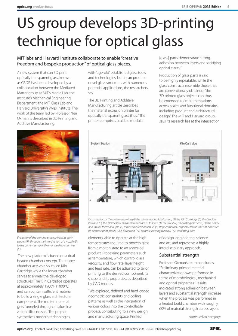
Evolution of the printing process: from its early stages (A), through the introduction of a nozzle (B), to the current setup with an annealing chamber (C).
elements, able to operate at the high temperatures required to process glass from a molten state to an annealed product. Processing parameters such as temperature, which control glass viscosity, and flow rate, layer height and feed rate, can be adjusted to tailor printing to the desired component, its shape and its properties, as described by CAD models.
”We explored, defined and hard-coded geometric constraints and coiling patterns as well as the integration of various colors into the controllable process, contributing to a new design and manufacturing space. Printed
[glass] parts demonstrate strong adhesion between layers and satisfying optical clarity.”
Production of glass parts is said to be highly repeatable, while the glass constructs resemble those that are conventionally obtained: “the 3D printed glass objects can thus be extended to implementations across scales and functional domains including product and architectural design.” The MIT and Harvard group says its research lies at the intersection
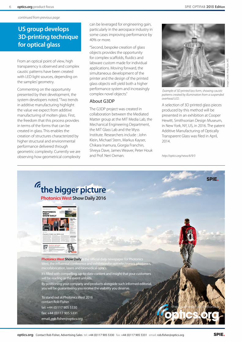
Cross-section of the system showing (A) the printer during fabrication, (B) the Kiln Cartridge (C) the Crucible Kiln and (D) the Nozzle Kiln. Detail elements are as follows: (1) the crucible, (2) heating elements, (3) the nozzle and (4) the thermocouple, (5) removable feed access lid (6) stepper motors (7) printer frame (8) Print Annealer (9) ceramic print plate (10) z-drive train (11) ceramic viewing window (12) insulating skirt.
of design, engineering, science and art, and represents a highly interdisciplinary approach.
Substantial strength
Professor Oxman’s team concludes, “Preliminary printed material characterization was performed in terms of morphological, mechanical and optical properties. Results indicated strong adhesion between layers and substantial strength increase when the process was performed in a heated build chamber with roughly 60% of material strength across layers.
continued on next page
optics.org product focus SPIE OPTIFAB 2015 Edition6
optics.org: Contact Rob Fisher, Advertising Sales tel: +44 (0)117 905 5330 fax: +44 (0)117 905 5331 email: [email protected]
From an optical point of view, high transparency is observed and complex caustic patterns have been created with LED light sources, depending on the samples’ geometry.
Commenting on the opportunity presented by their development, the system developers noted, “Two trends in additive manufacturing highlight the value we expect from additive manufacturing of molten glass. First, the freedom that this process provides in terms of the forms that can be created in glass. This enables the creation of structures characterized by higher structural and environmental performance delivered through geometric complexity. Currently we are observing how geometrical complexity
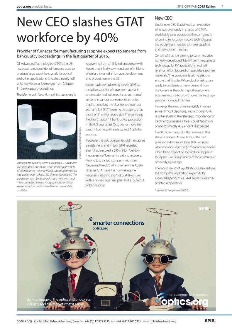
Example of 3D printed lass form, showing caustic patterns created by illumination from a suspended overhead LED.
Imag
e Cr
edit:
And
y Ry
an, M
IT.
can be leveraged for engineering gain, particularly in the aerospace industry in some cases improving performance by 40% or more.
“Second, bespoke creation of glass objects provides the opportunity for complex scaffolds, fluidics and labware custom made for individual applications. Moving forward, the simultaneous development of the printer and the design of the printed glass objects will yield both a higher performance system and increasingly complex novel objects.”
About G3DP
The G3DP project was created in collaboration between the Mediated Matter group at the MIT Media Lab, the Mechanical Engineering Department, the MIT Glass Lab and the Wyss Institute. Researchers include : John Klein, Michael Stern, Markus Kayser, Chikara Inamura, Giorgia Franchin, Shreya Dave, James Weaver, Peter Houk and Prof. Neri Oxman.
A selection of 3D printed glass pieces produced by this method will be presented in an exhibition at Cooper Hewitt, Smithsonian Design Museum, in New York, NY, US, in 2016. The patent Additive Manufacturing of Optically Transparent Glass was filed in April, 2014.
http://optics.org/news/6/9/3
continued from previous page
US group develops 3D-printing technique for optical glass
Photonics West Show Daily is the official daily newspaper for Photonics West, the influential conference and exhibition for optoelectronics, photonics, microfabrication, lasers and biomedical optics.
It’s filled with compelling, up-to-date content and insight that your customers will be reading as the event unfolds.
By positioning your company and products alongside such informed editorial, you will be guaranteeing you receive the visibility you deserve.
To stand out at Photonics West 2016contact Rob Fisher.
tel: +44 (0)117 905 5330
fax: +44 (0)117 905 5331
email: [email protected]
the bigger picturePhotonics West Show Daily 2016
TUESDAY, FEBRUARY 10, 2015
TUESDAYE D I T I O N
PHOTONICSWEST•SHOW DAILY
IN THIS ISSUE
DON’T MISS THESE EVENTS TODAY
TODAY’S NEWS
Chemistry Nobels wow BiOS crowdThe closest that the world of photonics has to rock stars played to a packed house at Sunday evening’s special plenary event on super-res-olution microscopy. Introduced by co-chair Bruce Tromberg as the very first BiOS Nobel session he predicted: “more will follow.”
Tromberg recalled the combination of excitement, pride and a little organization-al panic as fellow session chairs Ammasi Periasamy from the University of Virginia and PicoQuant’s Rainer Erdmann volleyed upwards of 50 emails back and forth in
preparation for the big night.Those who packed the Moscone’s room
134 to hear the 2014 chemistry laureates did not leave disappointed. Stefan Hell, honor-ing a long-standing speaking commitment, appeared by video message. And the sax-ophone-playing microscopist hit the right note when he said that the personal stories of the three laureates were quite different. For William “W.E.” Moerner, it has been a relatively conventional route to the Nobel. For Eric Betzig, not so much. His compelling tale
involves quitting Bell Labs in the 1990s and a period in the scientific wilderness before building a super-resolution microscope from spare parts in best friend Harald Hess’s living room. What all three had in common, said Hell, was a passion to work on things that “could not be done — supposedly.”
The story of super-resolution begins with another Nobel winner — 1933 physics lau-reate Erwin Schrödinger, who declared that the idea of observing individual molecules
PLENARY SESSIONSNANO/BIOPHOTONICS10:30–11:30 AM, ROOM 134Gabriel Popescu (Univ. of Illinois at Urbana-Champaign)
NEUROPHOTONICS 2–2:45 PM, ROOM 310 Thomas C. Südhof (Stanford Univ. School of Medicine)
INDUSTRY EVENTSSPIE Job Fair (10 AM–5 PM, South Exhibition Hall)
Financing life sciences and health care businesses (8:30–10 AM, Room 134)
ITAR workshop (10:30 AM–12:30 PM, Room 101)
3D printing panel (12:30–1:30 PM, Room 134)
Silicon photonics keynote and panel (1:30–3 PM, Room 134)
Intellectual property workshop/course (1:30–3:30 PM, Room 101)
See the technical program and exhibition guide for more details on daily events. Conference registration may be required. Industry events are open to all registration categories.
continued on page 03
3-4 BiOS conference and Expo news
9 Startup Challenge: the winners’ stories
21 Shuji Nakamura interview 27 Alex Cable: a philosophical
entrepreneur 34 Opto plenary report
Rock star status: 2014 Nobel laureates Eric Betzig (l) and William “W.E.” Moerner at Sunday night’s inau-gural BiOS Nobel plenary. Co-laureate Stefan Hell appeared by video link. Photos: Amy Nelson.
Pick up your complimentary copy of Celebrating Light
International Year of Light North Lower Lobby
BOOTH 1541TM
www.optikos.com Metrology and design: Anywhere light goes
We’re sporting a new look, but it’s still Optikos: providing cutting-edge metrology products and services for measuring lenses and camera systems; and expert design and manufacturing for optically-based product development.
Optikos has been solving complex optical problems for over thirty years, and our design and metrology solutions are chosen by clients in most every industry, field or application.
In the sky, under water, on screen, in your pocket.
TMAnywhere light goes
optics.org product focus SPIE OPTIFAB 2015 Edition 7
optics.org: Contact Rob Fisher, Advertising Sales tel: +44 (0)117 905 5330 fax: +44 (0)117 905 5331 email: [email protected]
GT Advanced Technologies (GTAT), the US-headquartered provider of furnaces used to produce large sapphire crystals for optical and other applications, is to shed nearly half of its workforce as it emerges from Chapter 11 bankruptcy proceedings.
The Merrimack, New Hampshire, company is
New CEO slashes GTAT workforce by 40%
recovering from an ill-fated encounter with Apple that initially saw hundreds of millions of dollars invested in furnace development and production in the US.
Apple had been planning to use GTAT as a captive supplier of sapphire material in unprecedented volumes for scratch-proof screens in various consumer electronics applications, but the deal turned sour last year and left GTAT burning through cash at a rate of $1 million every day. The company filed for Chapter 11 bankruptcy protection in the US courts last October - a move that caught both equity analysts and Apple by surprise.
However the two companies did then agree a settlement, and in July GTAT revealed that it had secured a $95 million “debtor-in-possession” loan on its path to recovery. Having just parted company with Tom Gutierrez, the CEO who oversaw the Apple disaster, GTAT says it is now taking the necessary steps to align its cost structure with a revised business plan and a route out of bankruptcy.
New CEOUnder new CEO David Keck, an executive who was previously in charge of GTAT’s worldwide sales operation, the company is returning to focus on its core technologies: the equipment needed to make sapphire and polysilicon materials.
On top of that, it is aiming to commercialize its newly developed “Merlin” cell interconnect technology for PV applications, and will retain an effort focused on specialty sapphire materials. “The company is taking steps to ensure that its solar PV product offerings are ready to capitalize on new demand from customers as the solar capital equipment business returns to growth over the next two years,” announced the firm.
However, the new plan inevitably involves some difficult decisions, and although GTAT is still evaluating the “strategic importance” of its other businesses, a headcount reduction of approximately 40 per cent is expected.
Exactly how many jobs that means at this stage is unclear. At one time, GTAT had planned to hire more than 1000 workers when building out the Arizona factory where it had been expecting to produce sapphire for Apple – although many of those were laid off nearly a year ago.
The latest round of layoffs should also reduce the company’s operating expenses by around 40 per cent as GTAT seeks to return to profitable operation.
http://optics.org/news/6/8/38
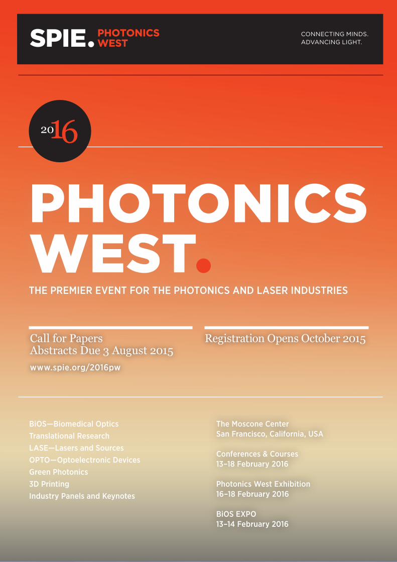
Through its Crystal Systems subsidiary, GT Advanced Technologies is one of the world’s leading providers of core sapphire material that is subsequently turned into wafers upon which LED chips are produced. The agreement with Soitec should see a new and much more cost-effective way to deposit light-emitting semiconductors on those wafers become widely available.
Provider of furnaces for manufacturing sapphire expects to emerge from bankruptcy proceedings in the first quarter of 2016.
Cred
it: G
T Ad
vanc
ed Te
chno
logi
es.
daily coverage of the optics and photonics industry and the markets that it serves
smarter connectionsoptics.org
optics.org product focus SPIE OPTIFAB 2015 Edition8
optics.org: Contact Rob Fisher, Advertising Sales tel: +44 (0)117 905 5330 fax: +44 (0)117 905 5331 email: [email protected]
The Moscone Center San Francisco, California, USA
Conferences & Courses 13–18 February 2016
Photonics West Exhibition16–18 February 2016
BiOS EXPO 13–14 February 2016
PHOTONICSWEST•
CONNECTING MINDS. ADVANCING LIGHT.
BiOS—Biomedical OpticsTranslational ResearchLASE —Lasers and SourcesOPTO—Optoelectronic DevicesGreen Photonics3D PrintingIndustry Panels and Keynotes
THE PREMIER EVENT FOR THE PHOTONICS AND LASER INDUSTRIES
Call for Papers Abstracts Due 3 August 2015
Registration Opens October 2015
www.spie.org/2016pw


![Welcome [] · 2019. 2. 22. · Welcome Welcome to the Award Winning Joseph A. Floreano Rochester Riverside Convention Center, seven time winner of Facilities Magazine’s Prime Site](https://img.pdfslide.us/doc/110x75/614139b983382e045471f29d/welcome-2019-2-22-welcome-welcome-to-the-award-winning-joseph-a-floreano.jpg)