Embed Size (px)
Citation preview
High performance primary side regulator (PSR) offline switchpower supply (SMPS) controller
MD1810/11/12/15 Datasheet
PRODUCT DESCRIPTIONMD181X is high performance primary sensing regulator (PSR) and monolithic switch power controller which is designed forMD181X is high performance primary sensing regulator (PSR) and monolithic switch power controller which is designed forsmall-power supply equipment with current mode control. Built-in accurate CV/CC control circuit, eliminates optocoupler, TL431and its related loop devices. High integration design, a high performance power BJT and PFM controller and all kinds ofprotection circuits in one chip, to minimize the peripheral components to save the cost greatly.MD181X can be simply designed a typical flyback switch converter, the unique driving technology promotes the characteristicsof withstand voltage and achieves excellent converting efficiency.
FEATURES
◆ Output voltage protection (OVP/UVP)
◆ Higher efficiency and meet Level 6 efficiency standards
FEATURES◆ Built-in 710V power BJT.
◆ PSR control, eliminates optocoupler and TL431
◆ Accurate CV/CC control
◆ Hysteresis over-temperature protection (OTP) circuit
◆ Quasi-resonant operation
Adapter
◆ Ultra-low start-up current
◆ Line under voltage protection(LUVP)
◆ < 100 mW no-load consumption @264Vac (5* rating)
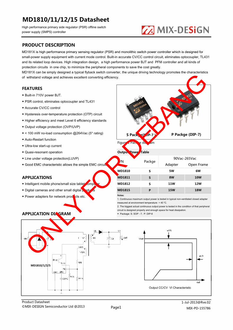
◆ Auto-Restart functionFigure�1�Packge�diagram
◆ Good EMC characteristic allows the simple EMC circuitP/N
Output Power Table
Packge90Vac-265Vac
Open Frame
◆ Output voltage protection (OVP/UVP)
S Packge(SOP-7 ) P Packge (DIP-7)
S
S
S
P 15W
Adapter
Notes:1. Continuous maximum output power is tested in typical non-ventilated closed adapter
d t i t t t 40 ℃
◆ Power adapters for network products etc.
◆ Digital cameras and other small digital products
MD1810
MD1811
◆ Intelligent mobile phone/small size tablet computer MD1812 11W 12W
6W
10W
18W
APPLICATIONS
◆ Good EMC characteristic allows the simple EMC circuit
5W
8W
MD1815
Open�Frame
APPLICATION DIAGRAM
measured at environment temperature + 40 ℃.2. The biggest actual continuous output power is tested in the condition of that peripheralcircuit is designed properly and enough space for heat dissipation.◆ Package: S: SOP - 7; P: DIP-8
MD1810/1/2/5
MIX-PD-155786
Product�Datasheet©MIX-DESIGN�Semiconductor�Ltd�@2013 Page1
Output CC/CV VI Characteristic
ONLY FO
R DEB
ANG

MD1810/11/12/15 Datasheet
PINOUT CONFIGURATION
High�performance�primary�side�regulator�(PSR)��offline�switchpower�supply�(SMPS)�controller
CPC
S
CPC
MD1815 MD1810/11/12
PIN Function Description
Figure�2.�Pin�Configuration�of�MD1810/11/12/15�(Top�view)
Pin # Name Function Description
5,�4 CSConntect external primary current sensing resistor RCS, the controller can detect theprimary current through the external sens resistor. When the voltage on the resistorachieves the maximum value, the internal power BJT will be turn off immediately.
to connect with a 100+nf capacitor the pin will become output cable drop
Power supplying pin of the controller, In order to let the controller gain more stablesupply voltage, the external filter capacitor must use low equivalent impedance (LowESR) of the electrolytic capacitor.
4 2Output feedback pin, to detect the output condition through the auxiliary winding voltage
1,�3 CPC to connect with a 100+nf capacitor, the pin will become output cable dropcompensation pin.
2,�1 VCC
4,�2 FB Output feedback pin, to detect the output condition through the auxiliary winding voltageof the transformer.
To connect the collector of internal power BJTHV�7-8,�5-6
6,- NC Not connected (Only for D Packge)
[email protected]�Datasheet©MIX-DESIGN�Semiconductor�Ltd�@2013
The referring grounding pin of the controller3,�8 GND
MIX-PD-155786Page2
ONLY FO
R DEB
ANG

MD1810/11/12/15 Datasheet
FUNCTIONAL BlOCK DIAGRAM
High�performance�primary�side�regulator�(PSR)�offline�switchpower�supply�(SMPS)�controller
Figure�3.Functional�block�diagram�of�MD1810/11/12/15
MIX-PD-155786
Product�Datasheet©MIX-DESIGN�Semiconductor�Ltd�@2013 Page3
ONLY FO
R DEB
ANG

MD1810/11/12/15 Datasheet
HV PIN Maximum Voltage Storage Temperature0 3 700V
High�performance�primary�side�regulator�(PSR)�offline�switchpower�supply�(SMPS)�controller
ABSOLUTE MAXIMUM RATINGS55 +150℃
MD1810
MD1811
MD1812
MD1815
1200mA
HV�PIN�Maximum�Voltage
VCC�Pin�Voltage 9V
IC�Peak�Current:
1500mA
Storage�Temperature�-0.3~700V
ESD(Human�Body�Model)800mA
600mA
Notes:
-55~+150℃
�+260℃/10S
2000V
Lead�Temperature
Others�Pin�Voltage��
Operating�Temperature�(Tj)��
ELECTRICAL CHARACTERISTICS
�0~�+150℃
Vcc�+�0.3V
7.5V
g
FB�Pin�Voltage1.All�voltages�referred�to�IC�GND�(TA=25℃),2.�Duration�not�exceed�2�msec.3.Instant�maximum�ratings�specified�will�not�cause�permanent�damageto�the�product,�while�long�maximum�ratings�specified�applied�will�doand�may�affect�product�reliability.
VDD-ON 7.5 8.0 8.5
VDD-OFF 3.0 3.3 3.5
IStar - 0.2 1
V
A
-
-
-
Shut down
Star-up Current
VDD UVLO
Star-up Voltage
UnitSymbol Min Type MaxConditionsParameter
IDD - 400 500
VDD-MAX - - 8.2V V
ICS 3.4 4 5 uA
VCS 500 mVCurrent Sense Threshold Voltage
uA
CURRENT SENSE SECTION
FB�Reference�Voltage
Max. Operating Voltage
-
Operating Current
-
Static�current
TLEB 500 - nS
VREF-FB 2.85 2.9 2.95 V
RFB 1.2 1.5 2 MΩ
VFB-MAX 5 V
FEEDBACK INPUT SECTION
Ic=1mA
Input�Resistance�of�FB�Pin
FB�Reference�Voltage
Leading Edge Blanking
Feedback�Threshold�Voltage
VCE(SAT) 0.3 V
VCEO 450 V
VCBO 700 V
T 130 135 140 ℃
Collector-emitter Voltage
Sh td T t
POWER BJT SECTION
Collector-emitter Saturation Voltage Io=1.0mA
Collector-Base�Voltage
OVER TEMPERATURE PROTECTION(OTP)
TSHDN 130 135 140 ℃
Shutdown�Temperature
Product�Datasheet©MIX-DESIGN�Semiconductor�Ltd�@2013 Page4
ONLY FO
R DEB
ANG

MD1810/11/12/15 DatasheetHigh�performance�primary�side�regulator�(PSR)�offline�switchpower�supply�(SMPS)�controller
FUNCTION DESCRIPTION When Toffs, the primary coil stores the energy, the outputfilter capacitor makes load discharge. In CC operation area,MD181X is specially designed for the charger/adapter of filter capacitor makes load discharge. In CC operation area,MD181X switch frequency will follow the output load directratio control detected by FB Voltage.
MD181X is specially designed for the charger/adapter ofsmall power digital products. To use PSR control technologyto provide accurate (CV/CC) characteristics. The controllerworks in PFM mode and the switching frequency can beautomaticially adjusted as per the load. Optimized drivingcircuit greatly promotes withstand voltage of the power BJTand minimizes the switching loss, so as to make the circuithave excellent converting efficiency.
The secondary rectifier diode peak current is determinatedby the peak current of primary-side inductance which alsoaffects the output current. The corresponding relation
g y
CONSTANT VOLTAGE(CV) OPERATIONWhen the circuit is operates in CV area, FB will detect theoutput voltage when the power BJT turn-off through thesensing voltage by auxiliary winding of the transformer, tomake the output voltage stablized in the fixed value. In theturn-on period of the output rectifier diode D,it's given theoutput winding voltage and auxiliary winding voltage as
Figure 5. Secondary Current Wavaform
affects the output current. The corresponding relationbetween the primary peak current and the secondary peakcurrent is as follows.
Vaux : auxiliary winding voltage;Nb:subsidiary winding turns;NS:output winding turns; Vd:forward voltage drop of output rectifier diode
output winding voltage and auxiliary winding voltage asfollows:
Ipk: primary peak current ; NP: primary winding turns; NS: secondary winding turns; Ipks:secondary peak current
FB will test the auxiliary winding voltage while the power BJToff-time to regulate the output voltage. In order to avoid thepeak influence happens in power BJT turn-off resulting fromthe leakage inductance of the transformer, and consideringthe accuracy of sampling voltage, FB captures the auxiliarywinding detection sampling points as below:
And primary inductance peak current is determinated by Pin4 to RCS resistance, the primary inductance peak currentand RCS resistance are in inverse proportion, so only needto adjust CS resistance to achieve different output currents.Output current Iout and primary current are given by:
output winding turns; Vd:forward voltage drop of output rectifier diodeIpk: primary peak current ; NP: primary winding turns; NS: secondary winding turns; Ipks:secondary peak current
MD181X built-in output cable drop compensation circuit.
OUTPUT CABLE COMPENSATION
Iout: Output current; Tons: secondary rectifier diode on-time; Toffs: secondary rectifier diode off-time
CONSTANT CURRENT(CC ) OPETATION
When it outputs different loads, the cable drop compensa-tion circuit provides cable drop voltage compensation whichis in fixed proportion with output voltage. The internal circuitwill generate one cable drop compensation signal once haveone 100nF capacitor connected with external Pin CPC.
MD181X CC control circuit is requested the converteroprating in DCM . In CC operation mode , the CC controlcircuit will fix the proportion between the Tons and Toffs PROTECTIVE FUNCTIONS
Figure 4.Auxiliary Voltage Wavaform
p pproduced by diode rectifier D. When Tons time, the primaryenergy of the transformer will be converted to the secondarywinding, via the rectifier diode then charge the outputcapacitor and supply load simultaneously.
Product�Datasheet©MIX-DESIGN�Semiconductor�Ltd�@2013
In order to guarantee a safe and reliable circuit to all occas-ions, MD181X built-in rich protection circuits, such as OCP,OVP, FB open-loop protection etc as intergration. Onceabnormality, it will come into protection mode.
Page5
ONLY FO
R DEB
ANG

MD1810/11/12/15 DatasheetHigh�performance�primary�side�regulator�(PSR)�offline�switchpower�supply�(SMPS)�controller
TYPICAL APPLICATION CIRCUIT
R1
﹣
R3
R4﹢
R5
R11
R10
- +
D1~D4 C1 C2
L2 T2
C4
D5D7
C6
CN1
85~265Vac
C8
Vo-
Vo+
﹣
R3
R4
R5
R9
R8
R11D1~D4 C1 C2
C3
D5
D6
D7
C6
U1�MD811
ST-CPCVCC
CS
HV
GND
FB
C5
CN1
Vo-
CPC
Figure�6.�Typical�application�of�MD1810�(Output:5V1A)
R7
R9
C3
U1�MD811
CSGND
FB
Position Q'ty Position Q'ty
��D1-D4 4 ��R4 11N4007��1A/1KV��DO-41 330K��1206��±5%
BOM LIST 5V1A Charger With MD1810
Description Description
��D5 1 ��R7 1
��D7 1 ��R5 1
��C1,C2 2 ��R8 1
��C4 1 ��R9 1
C5 1 R10 1
SB340��3A/40V�DO-15 200R��1206�±5%
102��1KV�±10% 22K�0805�±1%
10 F/16V 20% 5*11 2K 0805 5%
FR�107���1A/1KV��DO-41 1.3R�1206�±1%
4.7uF/400V�±20%��8*12 30K�0805�±1%
��C5 1 �R10 1
��C3 1 ��R11 1
��C6 2 ��L1 1
��C8 1 ��T1 1
��R1 1 ��U1 110R/1W�±5% MD1810SGB-TR��SOP-7
10uF/16V�±20%�5*11 2K�0805�±5%
104��25V�±10%�SMD 202R�0805�±5%
470uF/10V�±20%�6*12�Low�ESR 1mH�1W��Inductor
102/100V��0805 EE13�5+5��Transformer
��R3 1
Product�Datasheet©MIX-DESIGN�Semiconductor�Ltd�@2013
20M/1W��±5%
Page6Page6
ONLY FO
R DEB
ANG

MD1810/11/12/15 DatasheetHigh�performance�primary�side�regulator�(PSR)�offline�switchpower�supply�(SMPS)�controller
THERMAL IMPEDANCE
P (DIP 8) Packge Impedance(Reference only)P (DIP-8) Packge Impedance(Reference only)
(θJA)1.............................................................................................................................................................................................70℃/W�
(θJC)2.............................................................................................................................................................................................11℃/W
S (SOC-7) Packge Impedance(Reference only)
(θJA)1...........................................................................................................................................................................................100℃/W�
2. Measured on pin 7,8 (5.6) close to plastic interface(Power BJT Collector)
Notes: 1. Pin7 (5), 8 (6) Soldered to 2 oz. (610 g/m2) copper clad,as large area as possible.
(θJC)2.............................................................................................................................................................................................30℃/W
PART ORDERING INFORMATIONPART ORDERING INFORMATION
10�����MD1810
11�����MD1811
12�����MD1812
15�����MD1815
(Circuit Serial Type) Part Number
Package Identifier S������Plastic�SOP-7
P������Plastic�DIP-8�
T������Plastic�SOT-23
10�����MD1810
11�����MD1811
12�����MD1812
15�����MD1815
Cable compesation A: 0%; B: 4%,C: 6%; D: 9%
MD18 XX X X G -TR
Tape & Reel and Other Options Blank Tube‐TL Tape & Reel
Package Material Green: RoHS Compliant
Cable compesation A: 0%; B: 4%,C: 6%; D: 9%
Package Packing Type
Tape�&�Reel
Tape�&�Reel
T & R l
4000PCS
Part Number Marking ID on Body Minimum Pack
MD1812 4000PCS
S(SOP-7)
MD1810SXG-TR MD1810 4000PCS
MD1812SXG TR
MD1811SXG-TR MD1811
Tape�&�Reel
P(DIP-8) Tube
Product�Datasheet©MIX-DESIGN�Semiconductor�Ltd�@2013
MD1812 4000PCS
MD1815PXG MD1815 2000PCS/box
MD1812SXG-TR
Page�7
ONLY FO
R DEB
ANG

MD1810/11/12/15 DatasheetHigh�performance�primary�side�regulator�(PSR)�offline�switchpower�supply�(SMPS)�controller
MECHANICAL DIMENSIONS S-SOP-7
+
++++
Notes:1:Package dimensions conform to JEDEC specification :MS‐012; :Package outline exclusive of mold flash and metal burr;3:Package outline inclusive of plating thickness; :Datums A and B to be determined at datum plane H;5:Controlling dimensions are in Inches; Millineter sizes are shown in parenthesis; Angles in degrees;6:Minimum metal to metal spacing at the package body for the omitted lead location is 0.078 Inch(2.00mm);6:Pin locations start with Pin 1, and continue counter‐clock‐wise to pin 8 when viewed from the top. The notch and/or dimple are aids in locating Pin 1, Pin 7 is omitted;7:Lead width measured at package body;
++
Notes:1:Package dimensions conform to JEDEC apecification MS‐001‐AB(Issue B 7/85) for standard dual ‐in ‐line (DIP) package ;2:Contronlling dimensions are inches , Millineter sizes are shown in paretheses;3:Dimensions shown do not include mold flash or other protrusions .Mold flash or protrusions shall not exceed 0.006(0.15) on any side;4:Pin locations start with Pin 1, and continue counter‐clock‐wise to pin 8 when viewed from the top. The notch and/or dimple are aids in locating Pin 1, Pin 6 is omitted;5:Minimum metal to metal spacing at the package body for the omitted lead location is 0.137 Inch(3.48mm);6:Lead width measured at package body;7:Lead spacing measured with the leads constrained to be perpendieular to plane T;
+
++++
Notes:1:Package dimensions conform to JEDEC specification :MS‐012; :Package outline exclusive of mold flash and metal burr;3:Package outline inclusive of plating thickness; :Datums A and B to be determined at datum plane H;5:Controlling dimensions are in Inches; Millineter sizes are shown in parenthesis; Angles in degrees;6:Minimum metal to metal spacing at the package body for the omitted lead location is 0.078 Inch(2.00mm);6:Pin locations start with Pin 1, and continue counter‐clock‐wise to pin 8 when viewed from the top. The notch and/or dimple are aids in locating Pin 1, Pin 7 is omitted;7:Lead width measured at package body;
++
MECHANICAL DIMENSIONS P-DIP-7
p g , ;7:Lead width measured at package body;
Notes:1:Package dimensions conform to JEDEC apecification MS‐001‐AB(Issue B 7/85) for standard dual ‐in ‐line (DIP) package ;2:Contronlling dimensions are inches , Millineter sizes are shown in paretheses;3:Dimensions shown do not include mold flash or other
+
++++
Notes:1:Package dimensions conform to JEDEC specification :MS‐012; :Package outline exclusive of mold flash and metal burr;3:Package outline inclusive of plating thickness; :Datums A and B to be determined at datum plane H;5:Controlling dimensions are in Inches; Millineter sizes are shown in parenthesis; Angles in degrees;6:Minimum metal to metal spacing at the package body for the omitted lead location is 0.078 Inch(2.00mm);6:Pin locations start with Pin 1, and continue counter‐clock‐wise to pin 8 when viewed from the top. The notch and/or dimple are aids in locating Pin 1, Pin 7 is omitted;7:Lead width measured at package body;
++
Notes:1:Package dimensions conform to JEDEC apecification MS‐001‐AB(Issue B 7/85) for standard dual ‐in ‐line (DIP) package ;2:Contronlling dimensions are inches , Millineter sizes are shown in paretheses;3:Dimensions shown do not include mold flash or other protrusions .Mold flash or protrusions shall not exceed 0.006(0.15) on any side;4:Pin locations start with Pin 1, and continue counter‐clock‐wise to pin 8 when viewed from the top. The notch and/or dimple are aids in locating Pin 1, Pin 6 is omitted;5:Minimum metal to metal spacing at the package body for the omitted lead location is 0.137 Inch(3.48mm);6:Lead width measured at package body;7:Lead spacing measured with the leads constrained to be perpendieular to plane T;
+
++++
Notes:1:Package dimensions conform to JEDEC specification :MS‐012; :Package outline exclusive of mold flash and metal burr;3:Package outline inclusive of plating thickness; :Datums A and B to be determined at datum plane H;5:Controlling dimensions are in Inches; Millineter sizes are shown in parenthesis; Angles in degrees;6:Minimum metal to metal spacing at the package body for the omitted lead location is 0.078 Inch(2.00mm);6:Pin locations start with Pin 1, and continue counter‐clock‐wise to pin 8 when viewed from the top. The notch and/or dimple are aids in locating Pin 1, Pin 7 is omitted;7:Lead width measured at package body;
++
Notes:1:Package dimensions conform to JEDEC apecification MS‐001‐AB(Issue B 7/85) for standard dual ‐in ‐line (DIP) package ;2:Contronlling dimensions are inches , Millineter sizes are shown in paretheses;3:Dimensions shown do not include mold flash or other protrusions .Mold flash or protrusions shall not exceed 0.006(0.15) on any side;4:Pin locations start with Pin 1, and continue counter‐clock‐wise to pin 8 when viewed from the top. The notch and/or dimple are aids in locating Pin 1, Pin 6 is omitted;5:Minimum metal to metal spacing at the package body for the omitted lead location is 0.137 Inch(3.48mm);6:Lead width measured at package body;7:Lead spacing measured with the leads constrained to be perpendieular to plane T;
Product�Datasheet©MIX-DESIGN�Semiconductor�Ltd�@2013
ONLY FO
R DEB
ANG

CONTACT DETAILS
MD1810/11/12/15 DatasheetHigh�performance�primary�side�regulator�(PSR)�offline�switchpower�supply�(SMPS)�controller
8F,BlockB,Building 2,Creative Industry park, No.328 Xinghu street,Suzhou industrial park, Suzhou city, Jiangsu Provice,China.
Post:215143
MIX-DESIGN SEMICONDUCTOR TECHNOLOGY LIMITED
DISCLAIMER
Tel: (512) 6299 8099Fax: (512) 6299 8199Web:www.mix-designs.com
DISCLAIMER
MIX-DESIGN semiconductor technology limited reserves the right to make changes without further notice to any products orspecificationsherein.MIX-DESIGN semiconductor technology limited does not assume any responsibility for use of any itsproducts for anyparticular purpose, nor does MIX-DESIGN semiconductor technology limited assume any liability arising out ofthe application or useof any its products or circuits. MIX-DESIGN semiconductor technology limited does not convey any licenseunder its patent rights or other rights nor the rights of others.To obtain the most current product information availablevisit:www.mix-designs.com or contact us at the address shown above.
Version
Rev.01
Description
New Release
Date
15,Oct,2012
VERSION INFORMATIONS
Rev.02 Change the form,add. application informations 1,Jul,2013
SOUTH CHINA(Technical support and sevice Center)Room�1026-1031,�DongMing�Building,�MinkangRoad,�Longhua�new�district,�Shenzhen�city,�China.Tel:�(755)6182�6262;����Fax:�(755)6182�6292
SALES SUPPORT LOCATIONS
Product�Datasheet©MIX-DESIGN�Semiconductor�Ltd�@2013
( ) ; ( )
Page�9
ONLY FO
R DEB
ANG