Embed Size (px)
Citation preview
United States Patent [19] Hoover et al.
[11] [45] Date of
Patent Number: 4,555,414
[54]
[75]
[73]
[21] [22] [51] [52]
[58]
[56]
PROCESS FOR PRODUCING COMPOSITE PRODUCT HAVING PATTERNED METAL LAYER
Inventors: Merwin F. Hoover, Topsfield; Ann B. Salamone, Marblehead; Jan Vandebult, Tops?eld, all of Mass.
Polyonics Corporation, Newburyport, Mass.
Appl. N0.: 485,328 Filed: Apr. 15, 1983
Int. Cl.‘ ............................................. .. B05D 3/ 06
US. Cl. ................................ .. 427/43.1; 427/ 54.1; 427/98; 430/417
Field of Search ..................... .. 430/315, 414, 417; 427/43.l, 44, 54.1, 98
References Cited
U.S. PATENT DOCUMENTS
Assignee:
3,600,330 8/ 1971 Schneble et a1. ................. .. 252/430 3,775,176 11/1973 Cross et a1. . 117/227 3,779,758 12/1973 Polichette 430/ 315 3,863,244 I/ 1975 Lichtblau 340/280 3,900,320 8/1975 Rolker et a1. . . . . . . . . . . . .. 96/ 35.1
3,907,621 9/1975 Polichette et a1. ................ .. 430/414
3,925,578 12/1975 3,967,161 6/1976 4,006,047 2/ 1977 4,021,705 5/1977 4,073,981 4/1978 4,077,853 3/1978 4,089,993 5/1978 4,100,037 7/1978 4,133,908 1/1979 4,167,601 9/1979 4,181,750 1/1980 4,192,764 3/ 1980 4,216,246 8/1980 4,234,628 11/1980 4,268,536 5/1981 4,369,557 1/1983
Patent: Nov. 26, 1985
Polichette et a1. ................ .. 427/ 304
Lichtblau ........... .. 317/101 R
Brummett et a1. 156/656 Lichtblau ....... .. 361/402
Baron ............. .. 427/259
C011~Palagos .... .. 204/20
Shirahata et a1. 427/129 Baron et a1. . . . . . . . . . .. 204/ 15
Madsen ........................ .. 427/53
Beckenbaugh et a1, . .. 428/209
430/414 Beckenbaugh et a1. . ..
.. 430/455 Madsen .............. .. ..
Iwasaki et a1. 427/43.1 DuRose .............. .. 427/305
Beckenbaugh et a1. . 427/S4.1 Vandebult .................... 29/25.42
Primary Examiner—John H. Newsome Attorney, Agent, or Firm-Paul J. Cook
[57] ABSTRACI‘
A multilayered composite product including a base, a patterned cured resin bonded to the base and an applied metal layer selectively bonded to the patterned cured resin. The product is useful as an electrical circuit.
29 Claims, 8 Drawing Figures
U.S. Patent Nov. 26, 1985 Sheetl of4 4,555,414
U.S. Patent Nov. 26, 1985 Sheet2of4 4,555,414 ’
v 5Q \\\\\\\\\\\\\\\\\\\\\\\\, J‘ \ VII‘ . ililiiiliiiiiii ~ ////////// g, 4, k
mm 1 mm )v/ .w h
U.S. Patent‘ Nov. 26, 1985 Sheet3 of4 4,555,414
US. Patent Nov. 26, 1985 Sheet4of4 4,555,414
Fig. 7
60‘ 7O "7/ / 72/ w ‘m \w ~ Mae 74" *“33
64
Fig. 8
4,555,414 1
PROCESS FOR PRODUCING COMPOSITE PRODUCT HAVING PA'ITERNED METAL LAYER
BACKGROUND OF THE INVENTION
This invention relates to an article of manufacture having selective metal pathways and to a process for making the product wherein the metal pathways can function as an electrically conductive circuit.
Prior to the present invention, a wide variety of pro cesses has been available for forming electrically con ductive pathways on a non-electrically conducting sub strate. For example, a metal ?lm such as a ?lm formed from copper can be applied to a non-conducting sub strate to form a resultant laminate in a ?rst step. Typical substrates include rigid composites of ?ber glass and polyester or ?ber glass and epoxy or plastic ?lms of solvent resistant polyester or polyimide. In a commonly employed process, a layer of conductive metal such as copper is laminated to the non-conductive substrate in a ?rst step. A photoactivatible polymer (photoresist) then is coated on the metal layer and is subsequantly exposed to a light pattern using a light mask to reproduce the original metal pathway pattern desired followed by photoresist development and then metal etching in the area unprotected by the resist, thereby to produce the desired pattern. Alternatively, an etch resist can be directly printed such as by silk screen, gravure or the like on the metal laminate sheet followed by curing and then metal etching. This multistep process is slow and time-consuming and utilizes an expensive metal lami nated substrate such as a copper laminated substrate. An alternative presently available process comprises
direct circuit printing on a substrate utilizing a conduc tive metal-?lled thick ?lm ink or printing paste. In these processes, the conductive inks are limited to either very expensive silver or gold precious metals since they have the requisite high conductivity combined with resis tance to oxidation. Attempts to utilize these conductive inks with less expensive nickel, copper or aluminum powder, for example, have proven to be unsatisfactory for many applications since these metals, in the form of ?ne powders, do not provide the requisite conductivity primarily due to surface oxidation. The less expensive and highly conductive copper metal cannot be used in such a direct printing metal ink due to the rapid surface oxidation of the copper when in the form of ?ne powder such as ‘irregular particles, spheres or ?akes. Thus, this process is not amenable to manufacturing economical high conducting copper circuitry patterns.
In other processes, coatings containing noble or non noble metals or metal salts dispersed as particles, usually in a polymeric binder, function as seed sites for subse quent plating with a metal. The polymeric composition containing the metal or metal salt is applied to a sub strate in the desired pattern. After being applied or printed, the composition is heat cured in order to drive off solvent and to cross-link the polymer. The high temperatures, e.g. 160° C., and extended cure times, e.g. 1-2 hours, required for these products limits their use to products having good high temperature stability where the products are made by batch processes. Palladium is a typical activating material and is an expensive raw material that is only partially utilized since only the surface metal and the metal immediately adjacent to the surface is actually used to initiate plating. All the re maining buried metal is not utilized and therefore con stitutes an unnecessary expense. In addition to this ex
20
40
45
60
65
2 pense of overburden for metal ?lling, the availability and cost of precious/semiprecious material is volatile. Furthermore, printed lines only about 5 mils or greater are possible so that electrically conductive circuitry produced thereby is highly limited. Typical examples of these processes are disclosed, for example, in U.S. Pat. Nos. 3,900,320, 3,775,176 and 3,600,330.
It has also been proposed to form electrically conduc tive metal pathways by a process which includes coat ing a substrate with a composition containing a reduc ible metal complex. In one such process, a substrate is coated with a sorbitol copper formate solution contain ing a photoactivated reducing agent. Upon exposure to ultraviolet radiation, unmasked areas are reduced to copper metal and are suitable for plating nucleation sites. Non-exposed areas are washed clean and all cop per formate is removed before plating can be carried out. Although the photo-reducible copper solution is readily applied and selectively ultraviolet radiation treated, plating selectivity becomes a severe problem due to the high incidence of copper formate remaining on non-desired areas of the substrate. This results in a low reliability of the photo-selective copper reduction process. Examples of this technology are set forth in U.S. Pat. Nos. 4,268,536, 4,181,750, 4,133,908, 4,192,764, 4,167,601 and 3,925,578.
It has also been proposed to apply to a substrate non metal containing coatings which are subsequently acti vated for plating by surface treatment with noble and / or non-noble metals or metal salts. Typical examples of these processes are shown in U.S. Pat. Nos. 4,089,993, 4,073,981, 4,100,037 and 4,006,047. All of the coated substrates are heat cured and require elevated tempera tures for long cure times. Because of the use of palla dium, the cost of plating is relatively high. Examples of utilizing non-noble metals such as copper, nickel or cobalt are shown in U.S. Pat. Nos. 4,006,047, 4,077,853 and 4,234,628. These systems all require the interaction of at least two non-noble metals for rendering a surface receptive to plating and are limited to complete plating coverage of an article and are not utilized in selective printing and plating to form electrically conductive pathways. The above-described plating art is utilized primarily
to form electrical conducting metal pathways which function as electrical circuits in a wide variety of appli cations such as printed circuit boards using a relatively rigid base or so-called ?excircuits using a ?exible plastic base where the circuit is sandwiched between two lay ers of ?exible plastic. Typical bases for printed circuit boards include epoxy-?ber glass composites or phenol ic-?ber glass composites. Typical bases for ?excircuits include solvent-resistant polyimides and polyester. The polyimides, which are also high temperature stable, are very expensive. In forming such flexcircuits, the copper is laminated to the ?exible polymer base, and then selec tively etched to form the desired circuit. The printed circuit boards now utilized can be single sided, double sided or multilayer wherein electrically conductive paths are sandwiched between dielectric layers. The dielectric layer can be the rigid or ?exible substrate or a resist. Thus, in known subtractive processes, the poly mer base must be capable of withstanding the etching composition so that it is not degraded during circuit formation. The above-described plating processes also can be _
utilized to form thin ?exible resonant circuits which are
4,555,414 3
useful for electronic security and article theft detection systems. While these circuits are electrically conduc tive, in use they are passive in that they are not used primarily as current carrying devices. Article theft de tection systems are known in which electromagnetic waves are generated at a checkpoint and are caused to sweep repetitively at a given rate through a predeter— mined frequency range. A resonant electrical circuit tag is af?xed to articles to be protected, the electrical cir cuit being resonant at a frequency within the swept frequency range. Changes in energy level which occur at a speci?c frequency within the swept repeating fre quency band are detected, indicating presence of the tag in the ?eld. The electrical circuit comprises a coil and a capacitor connected to forma resonant loop. The tag circuit comprises an insulative substrate having one portion of the circuit formed on the opposite side of the substrate. Electrical connection is made between the portions of the circuit on opposite sides of the substrate by means of a conductive pin or eyelet extending through the substrate, or by means of a spot weld join ing confronting circuit areas as disclosed, for example, by US Pat. Nos. 3,863,244, 3,967,161, 4,021,705 and 4,369,557.
It would be highly desirable to provide a simpler, less costly and more rapid process for forming electrically conductive pathways on any one of a variety of non conducting substrates. Furthermore, it would be desir able to provide such a process which eliminates the “need for any metal etching step and which does not
I ‘require the use of high temperatures or extensive curing ‘time. By providing such a process, a wide variety of substrates, including thin ?lm substrates or rigid sub strates could be utilized to support electrically conduc tive paths. Such composite products could be utilized to produce metallized patterns such as those utilized on
" printed circuit boards, "multilayer boards, electronic ‘ "article surveillance circuit constructions utilized in arti ‘ cle theft detection systems, decorative articles or the
like.
SUMMARY OF THE INVENTION
In accordance with this invention, a composite article is provided comprising a base, a patterned cured resin bonded to the base and a metal layer bonded to the surface of the patterned cured resin to form patterned metal pathways. The metal pathways can be utilized to carry electrical current or can be utilized in a passive mode such as to form a resonant electrical circuit in response to electromagnetic waves at a given frequency such as in article theft detection devices, or can be merely decorative. The curable resin is coated on the substrate in the form of the desired pattern. It is then treated to activate the surface as by physically and/or chemically modifying the surface. The surface is then contacted with a catalytic metal composition capable of subsequently catalyzing the electroless deposition of metal on the patterned cured resin. The electrolessly deposited metal can, in turn, be coated with subsequent layers of metal, either electrolessly or electrolytically deposited. Composite articles having alternating multi ple layers of metal and non-metal can be formed by the process of this invention.
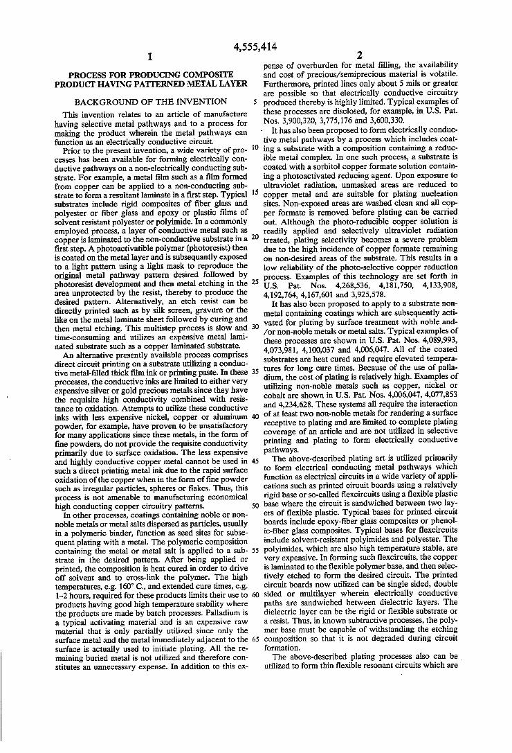
BRIEF DESCRIPTION OF THE DRAWINGS
FIG. 1 is a top view of a resonant tag electronic article surveillance (EAS) circuit made in accordance with this invention.
5
25
30
35
45
65
4 FIG. 2 is a bottom view of a resonant tag circuit made
in accordance with this invention. FIG. 3 is a cross-sectional view of the circuit of
FIGS. 1 and 2 along line 3-3. FIG. 4 is a cross-sectional view of a multilayer circuit
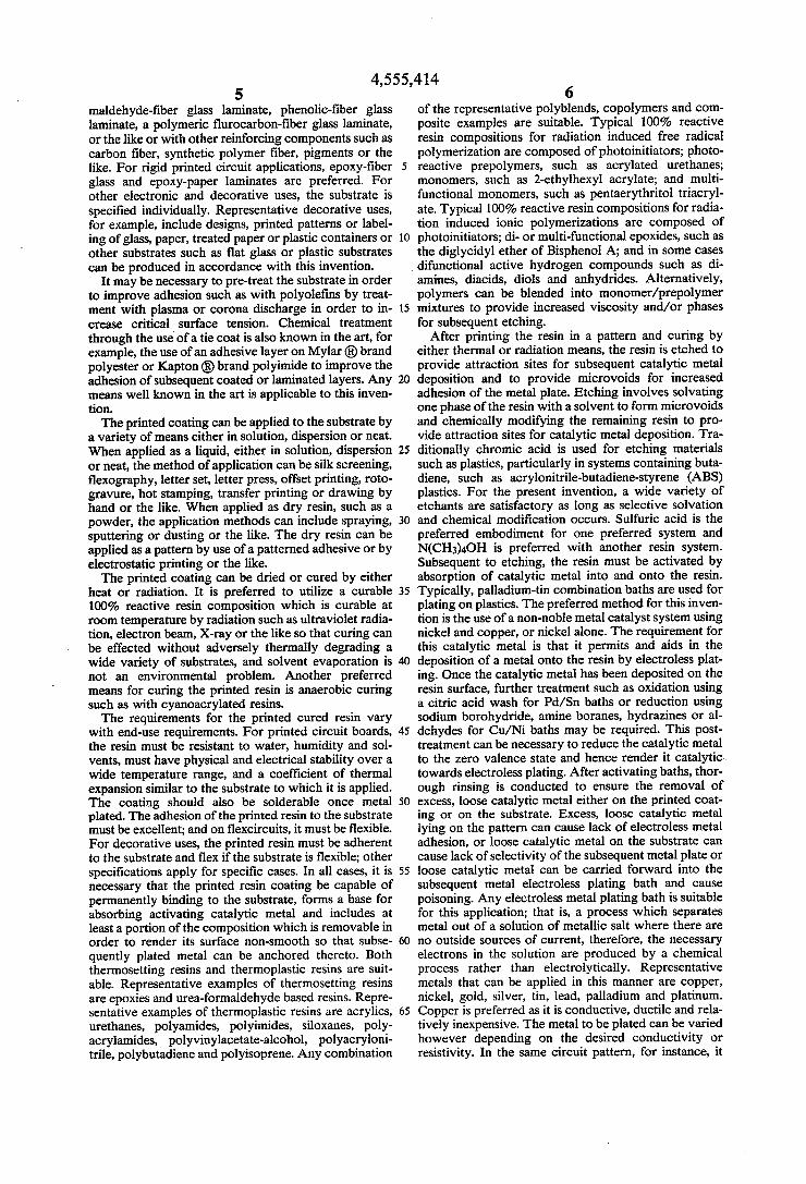
made in accordance with this invention. FIG. 5 is a top view of a ?exible circuit made in
accordance with this invention. FIG. 6 is a cross-sectional view of the ?exible circuit
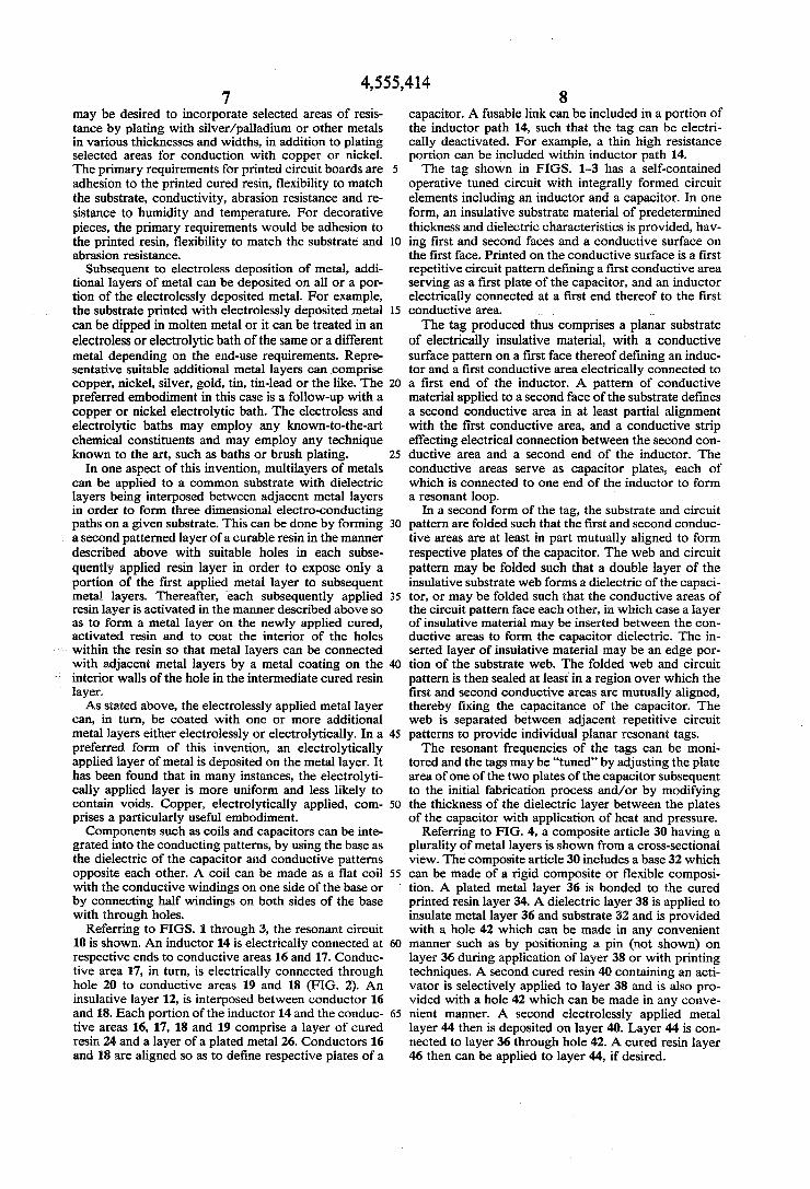
of this invention. FIG. 7 is a top view of a touch circuit mode in accor
dance with this invention. FIG. 8 is a cross-sectional view of the touch circuit
taken at line 8—8 of FIG. 7.
DESCRIPTION OF SPECIFIC EMBODIMENTS
In accordance with this invention, a curable resin composition is bonded to a substrate in the form of a pattern which pattern is the same as the ?nal desired metal pattern on the substrate. The curable resin com position must have suitable rheology to ensure retention of the printed pattern between the time of printing and subsequent curing, as for example, by being exposed to ultraviolet radiation, X-ray radiation, electron beam, heat or the like. The particular means for effecting cur= ing is chosen so that the substrate is not damaged. For example, when the substrate is a polymeric ?lm, it is preferred to employ ultraviolet radiation as a curing means and to avoid heating so that the ?lm is not dam aged. Once exposed to radiation or heat, the cured printed
resin is selectively etched to modify a portion of the surface rendering it receptive to catalytic metal deposi tion. The etched resin is contacted with a composition containing a catalytic metal or metal salt capable of subsequently catalyzing electroless deposition of the metal coating. If necessary, the adsorbed metal catalyst
. is reduced and then the pattern rinsed. After these steps are completed, the cured patterned resin has been physi cally and chemically modi?ed selectively so that elec troless deposition of metal thereon is effected selec tively without effecting deposition on the substrate. Further electroless or electrolytic plating can be used depending on end-use application. Any ?exible or rigid substrate can be utilized in the
process of this invention. Typical ?lm or relatively rigid substrates include polymeric compositions containing polyamide, polycarbonate, polyester, polyetherimide, polyimide, polynitrocellulose, polyole?ns such as poly ethylene, polypropylene, poly(ethylenevinylacetate), poly-Z-pentene, EPDM, polyionomers such as Sur lyn ®, polyphenylene oxide, polyphenylene sul?de, polysulfone, polystyrene, polyvinyl-vinylidine chloride or fluoride or the like. The preferred ?exible substrates include polycarbonates, polyesters, polyetherimides, polyimide, polyole?ns or polysulfone. Particularly for the ?exible printed circuit industry, substrates such as polyimides (KAPTON ®), polyesters (Mylar ®) poly carbonates (Lexan ®) and polyetherimides (Ultem ®) preferred due to their physical, electrical and thermal stability over wide temperature ranges, chemical inert ness and radiation resistance. For decorative uses, poly ole?ns and other less expensive substrates are preferred where temperature and other stress requirements are less. Alternatively, rigid substrates can include ceram ics, glass, plastics, paper compositions or the like; or composite substrates such as epoxy-?ber glass, epoxy paper laminate, paper-?ber glass laminate, urea for
4,555,414 5
maldehyde-?ber glass laminate, phenolic-?ber glass laminate, a polymeric flurocarbon-?ber glass laminate, or the like or with other reinforcing components such as carbon ?ber, synthetic polymer ?ber, pigments or the like. For rigid printed circuit applications, epoxy-?ber glass and epoxy-paper laminates are preferred. For other electronic and decorative uses, the substrate is speci?ed individually. Representative decorative uses, for example, include designs, printed patterns or label ing of glass, paper, treated paper or plastic containers or other substrates such as ?at glass or plastic substrates can be produced in accordance with this invention.
It may be necessary to pre-treat the substrate in order to improve adhesion such as with polyole?ns by treat ment with plasma or corona discharge in order to in crease critical surface tension. Chemical treatment through the use‘ of a tie coat is also known in the art, for example, the use of an adhesive layer on Mylar ® brand polyester or Kapton ® brand polyimide to improve the adhesion of subsequent coated or laminated layers. Any means well known in the art is applicable to this inven tion. The printed coating can be applied to the substrate by
a variety of means either in solution, dispersion or neat. When applied as a liquid, either in solution, dispersion or neat, the method of application can be silk screening, flexography, letter set, letter press, offset printing, roto gravure, hot stamping, transfer printing or drawing by hand or the like. When applied as dry resin, such as a powder, the application methods can include spraying, sputtering or dusting or the like. The dry resin can be applied as a pattern by use of a patterned adhesive or by electrostatic printing or the like. The printed coating can be dried or cured by either
heat or radiation. It is preferred to utilize a curable 100% reactive resin composition which is curable at room temperature by radiation such as ultraviolet radia tion, electron beam, X-ray or the like so that curing can be effected without adversely thermally degrading a wide variety of substrates, and solvent evaporation is not an environmental problem. Another preferred means for curing the printed resin is anaerobic curing such as with cyanoacrylated resins. The requirements for the printed cured resin vary
with end-use requirements. For printed circuit boards, the resin must be resistant to water, humidity and sol vents, must have physical and electrical stability over a wide temperature range, and a coef?cient of thermal expansion similar to the substrate to which it is applied. The coating should also be solderable once metal plated. The adhesion of the printed resin to the substrate must be excellent; and on ?excircuits, it must be flexible. For decorative uses, the printed resin must be adherent to the substrate and ?ex if the substrate is ?exible; other speci?cations apply for speci?c cases. In all cases, it is necessary that the printed resin coating be capable of permanently binding to the substrate, forms a base for absorbing activating catalytic metal and includes at least a portion of the composition which is removable in order to render its surface non-smooth so that subse quently plated metal can be anchored thereto. Both thermosetting resins and thermoplastic resins are suit able. Representative examples of thermosetting resins are epoxies and urea-formaldehyde based resins. Repre sentative examples of thermoplastic resins are acrylics, urethanes, polyamides, polyimides, siloxanes, poly acrylamides, polyvinylacetate-alcohol, polyacryloni trile, polybutadiene and polyisoprene. Any combination
25
30
40
60
65
6 of the representative polyblends, copolymers and com posite examples are suitable. Typical 100% reactive resin compositions for radiation induced free radical polymerization are composed of photoinitiators; photo reactive prepolymers, such as acrylated urethanes; monomers, such as Z-ethylhexyl acrylate; and multi functional monomers, such as pentaerythritol triacryl ate. Typical 100% reactive resin compositions for radia tion induced ionic polymerizations are composed of photoinitiators; di- or multi-functional epoxides, such as the diglycidyl ether of Bisphenol A; and in some cases
_ difunctional active hydrogen compounds such as di amines, diacids, diols and anhydrides. Alternatively, polymers can be blended into monomer/prepolymer mixtures to provide increased viscosity and/or phases for subsequent etching.
After printing the resin in a pattern and curing by either thermal or radiation means, the resin is etched to provide attraction sites for subsequent catalytic metal deposition and to provide microvoids for increased adhesion of the metal plate. Etching involves solvating one phase of the resin with a solvent to form microvoids and chemically modifying the remaining resin to pro vide attraction sites for catalytic metal deposition. Tra ditionally chromic acid is used for etching materials such as plastics, particularly in systems containing buta diene, such as acrylonitrile-butadiene-styrene (ABS) plastics. For the present invention, a wide variety of etchants are satisfactory as long as selective solvation and chemical modi?cation occurs. Sulfuric acid is the preferred embodiment for one preferred system and N(CH3)4OH is preferred with another resin system. Subsequent to etching, the resin must be activated by absorption of catalytic metal into and onto the resin. Typically, palladium-tin combination baths are used for plating on plastics. The preferred method for this inven tion is the use of a non-noble metal catalyst system using nickel and copper, or nickel alone. The requirement for this catalytic metal is that it permits and aids in the deposition of a metal onto the resin by electroless plat ing. Once the catalytic metal has been deposited on the resin surface, further treatment such as oxidation using a citric acid wash for Pd/Sn baths or reduction using sodium borohydride, amine boranes, hydrazines or al dehydes for Cu/Ni baths may be required. This post treatment can be necessary to reduce the catalytic metal to the zero valence state and hence render it catalytic towards electroless plating. After activating baths, thor ough rinsing is conducted to ensure the removal of excess, loose catalytic metal either on the printed coat ing or on the substrate. Excess, loose catalytic metal lying on the pattern can cause lack of electroless metal adhesion, or loose catalytic metal on the substrate can cause lack of selectivity of the subsequent metal plate or loose catalytic metal can be carried forward into the subsequent metal electroless plating bath and cause poisoning. Any electroless metal plating bath is suitable for this application; that is, a process which separates metal out of a solution of metallic salt where there are no outside sources of current, therefore, the necessary electrons in the solution are produced by a chemical process rather than electrolytically. Representative metals that can be applied in this manner are copper, nickel, gold, silver, tin, lead, palladium and platinum. Copper is preferred as it is conductive, ductile and rela tively inexpensive. The metal to be plated can be varied however depending on the desired conductivity or resistivity. In the same circuit pattern, for instance, it
4,555,414 7
may be desired to incorporate selected areas of resis tance by plating with silver/palladium or other metals in various thicknesses and widths, in addition to plating selected areas for conduction with copper or nickel. The primary requirements for printed circuit boards are adhesion to the printed cured resin, flexibility to match the substrate, conductivity, abrasion resistance and re sistance to humidity and temperature. For decorative pieces, the primary requirements would be adhesion to the printed resin, ?exibility to match the substrate and abrasion resistance.
Subsequent to electroless deposition of metal, addi tional layers of metal can be deposited on all or a por tion of the electrolessly deposited metal. For example, the substrate printed with electrolessly deposited metal can be dipped in molten metal or it can be treated in an electroless or electrolytic bath of the same or a different metal depending on the end-use requirements. Repre sentative suitable additional metal layers can comprise copper, nickel, silver, gold, tin, tin-lead or the like. The preferred embodiment in this case is a follow-up with a copper or nickel electrolytic bath. The electroless and electrolytic baths may employ any known-to-the-art chemical constituents and may employ any technique known to the art, such as baths or brush plating.
In one aspect of this invention, multilayers of metals can be applied to a common substrate with dielectric layers being interposed between adjacent metal layers in order to form three dimensional electro-conducting paths on a given substrate. This can be done by forming
, a second patterned layer of a curable resin in the manner described above with suitable holes in each subse quently applied resin layer in order to expose only a portion of the ?rst applied metal layer to subsequent metal layers. Thereafter, each subsequently applied resin layer is activated in the manner described above so as to form a metal layer on the newly applied cured, activated resin and to coat the interior of the holes
» within the resin so that metal layers can be connected with adjacent metal layers by a metal coating on the interior walls of the hole in the intermediate cured resin layer. As stated above, the electrolessly applied metal layer
can, in turn, be coated with one or more additional metal layers either electrolessly or electrolytically. In a preferred form of this invention, an electrolytically applied layer of metal is deposited on the metal layer. It has been found that in many instances, the electrolyti cally applied layer is more uniform and less likely to contain voids. Copper, electrolytically applied, com prises a particularly useful embodiment. Components such as coils and capacitors can be inte
grated into the conducting patterns, by using the base as the dielectric of the capacitor and conductive patterns opposite each other. A coil can be made as a ?at coil with the conductive windings on one side of the base or by connecting half windings on both sides of the base with through holes.
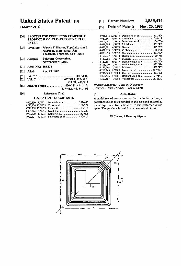
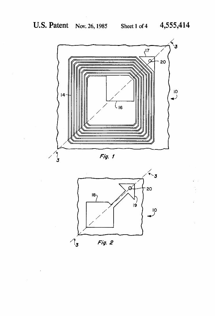
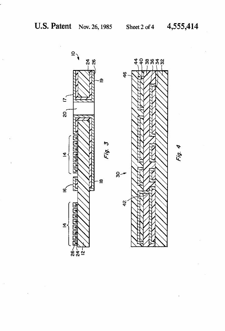
Referring to FIGS. 1 through 3, the resonant circuit 10 is shown. An inductor 14 is electrically connected at respective ends to conductive areas 16 and 17. Conduc tive area 17, in turn, is electrically connected through hole 20 to conductive areas 19 and 18 (FIG. 2). An insulative layer 12, is interposed between conductor 16 and 18. Each portion of the inductor 14 and the conduc tive areas 16, 17, 18 and 19 comprise a layer of cured resin 24 and a layer of a plated metal 26. Conductors l6 and 18 are aligned so as to de?ne respective plates of a
0
20
40
45
60
65
8 capacitor. A fusable link can be included in a portion of the inductor path 14, such that the tag can be electri cally deactivated. For example, a thin high resistance portion can be included within inductor path 14. The tag shown in FIGS. 1-3 has a self-contained
operative tuned circuit with integrally formed circuit elements including an inductor and a capacitor. In one form, an insulative substrate material of predetermined thickness and dielectric characteristics is provided, hav ing ?rst and second faces and a conductive surface on the ?rst face. Printed on the conductive surface is a ?rst repetitive circuit pattern de?ning a ?rst conductive area serving as a ?rst plate of the capacitor, and an inductor electrically connected at a ?rst end thereof to the ?rst conductive area. The tag produced thus comprises a planar substrate
of electrically insulative material, with a conductive surface pattern on a ?rst face thereof de?ning an induc tor and a ?rst conductive area electrically connected to a ?rst end of the inductor. A pattern of conductive material applied to a second face of the substrate de?nes a second conductive area in at least partial alignment with the first conductive area, and a conductive strip effecting electrical connection between the second con ductive area and a second end of the inductor. The conductive areas serve as capacitor plates, each of which is connected to one end of the inductor to form a resonant loop. '
In a second form of the tag, the substrate and circuit pattern are folded such that the ?rst and second conduc tive areas are at least in part mutually aligned to form respective plates of the capacitor. The web and circuit pattern may be folded such that a double layer of the insulative substrate web forms a dielectric of the capaci tor, or may be folded such that the conductive areas of the circuit pattern face each other, in which case a layer of insulative material may be inserted between the con ductive areas to form the capacitor dielectric. The in serted layer of insulative material may be an edge por tion of the substrate web. The folded web and circuit pattern is then sealed at least in a region over which the ?rst and second conductive areas are mutually aligned, thereby ?xing the capacitance of the capacitor. The web is separated between adjacent repetitive circuit patterns to provide individual planar resonant tags. The resonant frequencies of the tags can be moni
tored and the tags may be “tuned” by adjusting the plate area of one of the two plates of the capacitor subsequent to the initial fabrication process and/or by modifying the thickness of the dielectric layer between the plates of the capacitor with application of heat and pressure.
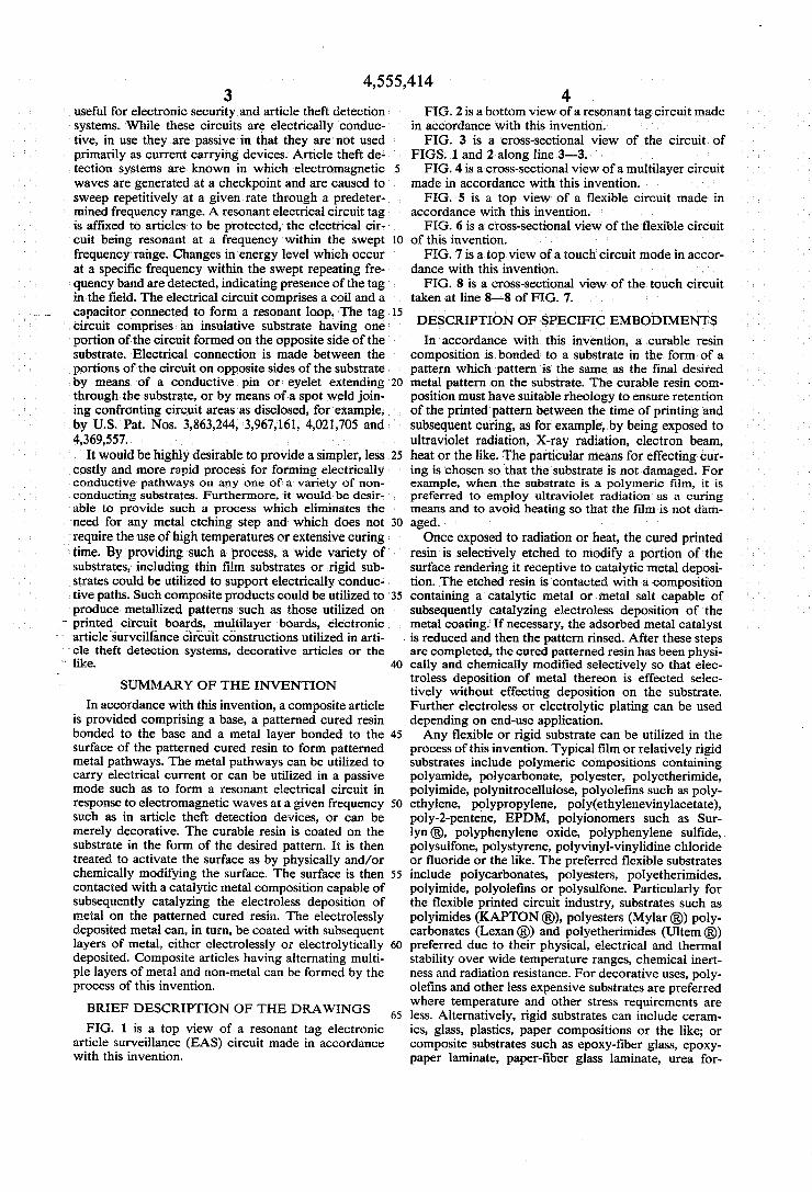
Referring to FIG. 4, a composite article 30 having a plurality of metal layers is shown from a cross-sectional view. The composite article 30 includes a base 32 which can be made of a rigid composite or flexible composi tion. A plated metal layer 36 is bonded to the cured printed resin layer 34. A dielectric layer 38 is applied to insulate metal layer 36 and substrate 32 and is provided with a hole 42 which can be made in any convenient manner such as by positioning a pin (not shown) on layer 36 during application of layer 38 or with printing techniques. A second cured resin 40 containing an acti vator is selectively applied to layer 38 and is also pro vided with a hole 42 which can be made in any conve nient manner. A second electrolessly applied metal layer 44 then is deposited on layer 40. Layer 44 is con nected to layer 36 through hole 42. A cured resin layer 46 then can be applied to layer 44, if desired.
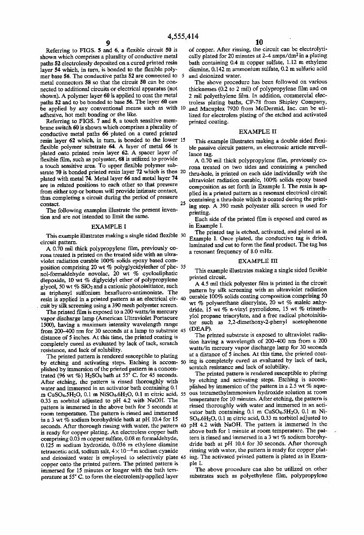
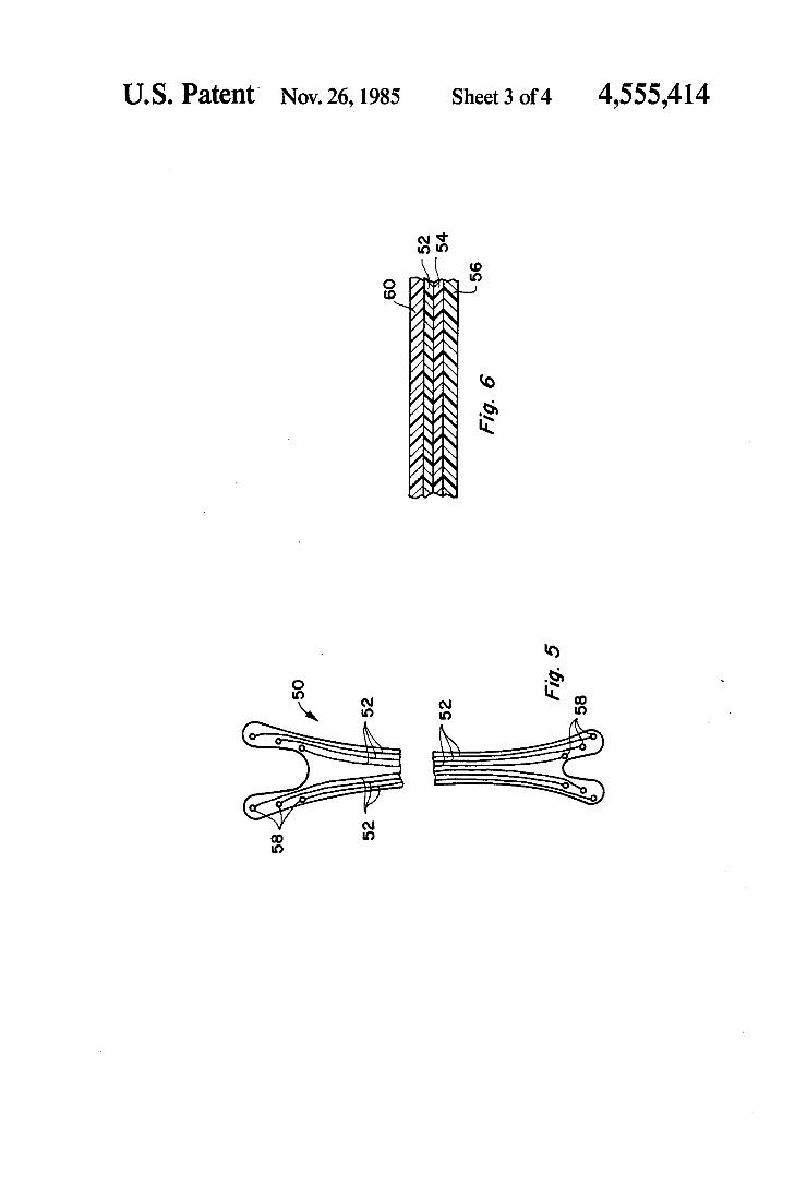
4,555,414 Referring to FIGS. 5 and 6, a ?exible circuit 50 is
shown which comprises a plurality of conductive metal paths 52 electrolessly deposited on a cured printed resin layer 54 which, in turn, is bonded to the ?exible poly mer base 56. The conductive paths 52 are connected to metal connectors 58 so that the circuit 50 can be con nected to additional circuits or electrical apparatus (not shown). A polymer layer 60 is applied to coat the metal paths 52 and to be bonded to base 56. The layer 60 can be applied by any conventional means such as with adhesive, hot melt bonding or the like.
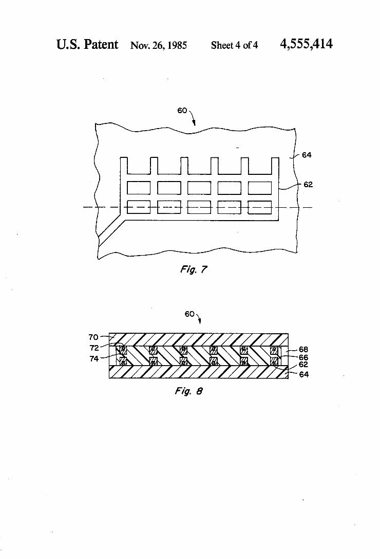
Referring to FIGS. 7 and 8, a touch sensitive mem brane switch 60 is shown which comprises a plurality of conductive metal paths 66 plated on a cured printed resin layer 62 which, in turn, is bonded to the lower ?exible polymer substrate 64. A layer of metal 66 is plated onto printed resin layer 62. A spacer layer of ?exible ?lm, such as polyester, 68 is utilized to provide a touch sensitive area. To upper ?exible polymer sub strate 70 is bonded printed resin layer 72 which is then plated with metal 74. Metal layer 66 and metal layer 74 are in related positions to each other so that pressure from either top or bottom will provide intimate contact, thus completing a circuit during the period of pressure contact. The following examples illustrate the present inven
tion and are not intended to limit the same.
EXAMPLE I
This example illustrates making a single sided ?exible circuit pattern. A 0.70 mil thick polypropylene ?lm, previously co
rona treated is printed on the treated side with an ultra~ violet radiation curable 100% solids epoxy based com position comprising 20 wt % polyglycidylether of phe nol-formaldehyde novolac, 20 wt % cycloaliphatic diepoxide, 10 wt % diglycidyl ether of polypropylene glycol, 50 wt % SiOz and a cationic photoinitiator, such as triphenyl sulfonium hexa?uoro-antimoniate. The resin is applied in a printed pattern as an electrical cir cuit by silk screening using a 390 mesh polyester screen. The printed ?lm is exposed to a 200 watts/ in mercury
vapor discharge lamp (American Ultraviolet Portacure 1500), having a maximum intensity wavelength range from 200-400 nm for 30 seconds at a lamp to substrate distance of 5 inches. At this time, the printed coating is completely cured as evaluated by lack of tack, scratch resistance, and lack of solubility. The printed pattern is rendered susceptible to plating
by etching and activating steps. Etching is accom plished by immersion of the printed pattern in a concen trated (96 wt %) H2804 bath at 55° C. for 45 seconds. After etching, the pattern is rinsed thoroughly with water and immersed in an activator bath containing 0.1 m CuSO4.5H2O, 0.1 m NiSO4.6H2O, 0.1 m citric acid, 0.33 m sorbitol adjusted to pH 4.2 with NaOH. The pattern is immersed in the above bath for 5 seconds at room temperature. The pattern is rinsed and immersed in a 3 wt % sodium borohydride bath at pH 10.4 for 15 seconds. After thorough rinsing with water, the pattern is ready for copper plating. An electroless copper bath comprising 0.03 in copper sulfate, 0.08 m formaldehyde, 0.125 m sodium hydroxide, 0.036 m ethylene diamine tetraacetic acid, sodium salt, 4X 10⁴m sodium cyanide and deionized water is employed to selectively plate copper onto the printed pattern. The printed pattern is immersed for 15 minutes or longer with the bath tem perature at 55° C. to form the electrolessly-applied layer
25
40
45
50
60
65
10 of copper. After rinsing, the circuit can be electrolyti cally plated for 20 minutes at 2-4 amps/dm2 in a plating bath containing 0.4 m copper sulfate, 1.12 m ethylene diamine, 0.142 m ammonium sulfate, 0.2 m sulfuric acid and deionized water. The above procedure has been followed on various
thicknesses (0.2 to 2 mil) of polypropylene ?lm and on 2 mil polyethylene ?lm. In addition, commercial elec troless plating baths, CP-78 from Shipley Company, and Macuplex 7920 from McDermid, Inc. can be uti lized for electroless plating of the etched and activated printed coating.
EXAMPLE II
This example illustrates making a double sided ?exi ble passive circuit pattern, an electronic article surveil lance tag. A 0.70 mil thick polypropylene ?lm, previously co
rona treated on two sides and containing a punched thru-hole, is printed on each side individually with the ultraviolet radiation curable, 100% solids epoxy based composition as set forth in Example I. The resin is ap plied in a printed pattern as a resonant electrical circuit containing a thru-hole which is coated during the print ing step. A 390 mesh polyester silk screen is used for printing.
, Each side of the printed ?lm is exposed and cured as in Example I. The printed tag is etched, activated, and plated as in
Example I. Once plated, the conductive tag is dried, laminated and cut to form the ?nal product. The tag has a resonant frequency of 8.0 mHz.
EXAMPLE 111
This example illustrates making a single sided ?exible printed circuit. A 4.5 mil thick polyester ?lm is printed in the circuit
pattern by silk screening with an ultraviolet radiation curable 100% solids coating composition comprising 50 wt % polyurethane diacrylate, 20 wt % maleic anhy dride, 15 wt % n-vinyl pyrrolidone, 15 wt % trimeth ylol propane triacrylate, and a free radical photoinitia tor such as 2,2-dimethoxy-2-phenyl acetophenone
(DEAP). The printed substrate is exposed to ultraviolet radia
tion having a wavelength of 200-400 nm from a 200 watts/in mercury vapor discharge lamp for 30 seconds at a distance of 5 inches. At this time, the printed coat ing is completely cured as evaluated by lack of tack, scratch resistance and lack of solubility. The printed pattern is rendered susceptible to plating
by etching and activating steps. Etching is accom plished by immersion of the pattern in a 2.5 wt % aque ous tetramethylammonium hydroxide solution at room temperature for 10 minutes. After etching, the pattern is rinsed thoroughly with water and immersed in an acti vator bath containing 0.1 m CuSO4.5H2O, 0.1 m Ni SO4.6H2O, 0.1 m citric acid, 0.33 m sorbitol adjusted to pH 4.2 with NaOH. The pattern is immersed in the above bath for 1 minute at room temperature. The pat— tern is rinsed and immersed in a 3 wt % sodium borohy dride bath at pH 10.4 for 30 seconds. After thorough rinsing with water, the pattern is ready for copper plat ing. The activated printed pattern is plated as in Exam ple I. -. The above procedure can also be utilized on other
substrates such as polyethylene ?lm, polypropylene
4,555,414 11
?lm, polyimide'?lm, polycarbonate ?lm, polyetheri mide ?lm or polysulfone ?lm.
EXAMPLE IV
This example illustrates making a double sided ?exi ble printed circuit. A 0.75 mil thick polypropylene ?lm, previously co
rona treated on two sides, and containing a punched thru-hole, is printed by silk screening on each side indi vidually with the ultraviolet radiation curable composi tion of Example III. A 390 mesh polyester silk screen is used. Each side of the ?lm is exposed and cured as in Exam
ple III. , The double sided printed circuit is etched, activated
and plated as in Example III. Once plated, the conduc tiv_e pattern is ready for further fabrication to form a completed ?ex circuit.
EXAMPLE V
This example illustrates making a multilayer circuit. A 0.75 mil thick composite polypropylene ?lm con
sisting of a polypropylene inner layer and surface coated on two sides with a polyethylene/propylene resin and corona treated on two sides and containing a punched thru-hole, is printed by silk screening on each side individually with the ultraviolet radiation curable composition of Example I. The printed ?lm is exposed, cured, etched, activated
and plated as in Example II. After drying, the conductive double sided circuit is
then heat laminated on each side with the above-treated composite polypropylene ?lm containing a punched thru-hole. A second circuit pattern is printed by silk screening on each side individually of the double sided circuit with the ultraviolet radiation curable composi tion of Example ,I. ‘The printed second layer of the multilayer circuit is
exposed, cured, etched, activated and plated as in Ex ample II. At this point, four layers of conductive cir cuitry are formed.
This procedure may be repeated as necessary to in crease the number of layers for a desired ?nal multilayer circuit.
Using the ultraviolet radiation curable composition and procedure of Example III, other substrates can be utilized such as polyester, polyimide, polycarbonate, polyetherimide or polysulfone utilizing other lamina tion means such as solvents or adhesives. Rigid sub strates such as epoxy-?ber glass and phenolic-?ber glass laminates can also be utilized; any combination of ?exi ble and rigid substrates are suitable for the fabrication of multilayer circuits using the process of this invention and appropriate laminating means.
EXAMPLE VI
This example illustrates making a single sided rigid printed circuit board. A 56 mil‘ thick epoxy-?ber glass board is printed with
the ultraviolet radiation curable composition of Exam ple III. The printed board is exposed, cured, etched, activated and plated as in Example III. The above procedure can also be utilized on other
rigid substrates such as urea formaldehyde-?ber glass and phenolic-?ber glass laminates.
' In addition, touch sensitive switches such as in key board and membrane circuits can be fabricated using the ultraviolet radiation curable composition and proce
30
40
45
55
60
65
12 dure of Example III utilizing substrates such as polyole ?ns, polyesters, polyimides, polycarbonates, polyetheri mides or polysulfones. We claim: 1. The process for forming a composite product
which comprises applying directly to a base a patterned layer of curable resin, curing said resin in said pattern, etching said patterned cured resin in the absence of a mask with an etchant which will permit absorption onto said patterned cured resin of a metal catalyst capable of promoting electroless metal deposition selectively but which will not chemically modify said base so as to permit absorption onto said base of a metal catalyst capable of promoting electroless metal deposition selec tively, contacting said etched cured resin with a catalyst composition capable of promoting electroless metal deposition on said etched cured resin without effecting, absorption of said catalyst on said base, activating the absorbed catalyst, and electrolessly depositing a metal layer on said etched cured patterned resin selectively without effecting electroless deposition of saidmetal layer on the base.
2. The process of claim 1 wherein said base is a ?exi ble substrate.
3. The process of claim 1 wherein said base is a rigid substrate.
4. The process of claim 1 wherein said metal layer is copper.
5. The process of claim 1 wherein said catalyst com position comprises copper and nickel.
6. The process of claim 1 wherein said catalyst com position comprises copper and nickel boride.
7. The process of claim 1 wherein said catalyst com position comprises nickel boride.
8'. The process of claim 1 wherein said catalyst com position comprises palladium andtin.
9. The process of claim 1 wherein said curing is ef fected with electron beam radiation.
10. The process of claim 1 wherein said curing is effected thermally.
11. The process of claim 1 wherein said curing is effected with ultraviolet radiation.
12. The process of claim 1 wherein said curing is effected with ultraviolet radiation and wherein said metal layer is copper.
13. The process of claim 1 wherein said base com prises a polyimide composition.
14. The process of claim 1 wherein said base com prises a polyester composition.
15. The process of claim 1 wherein said base com prises a polyole?n composition.
16. The processof claim 1 wherein said base com prises a polycarbonate composition.
17. The process of claim 1 wherein said base com prises a polyetherimide composition.
18. The process of claim 1 wherein said substrate comprises a composite of a resin and a reinforcing com ponent.
19. The process of claim 1 wherein the reinforcing component is ?ber glass. ,
20. The process of claim 1 wherein said substrate comprises a composite or resin and paper.
21. The process of claim 1 wherein said substrate comprises a composite of an epoxy resin and ?ber glass.
22. The process of claim 1 wherein said substrate comprises a composite of an epoxy resin and paper.
4,555,414 13
23. The process of claim 1 wherein said patterned
cured resin composition comprises an epoxy containing
resin composition. 24. The process of claim 1 wherein said patterned
cured resin composition comprises an acrylic contain
ing resin composition. 25. The process of claim 1 wherein said patterned
cured resin composition comprises a polyimide contain
ing resin composition.
20
25
30
35
45
50
55
60
65
14 26. The process of claim 1 wherein said patterned
cured resin composition comprises an unsaturated poly ole?n containing resin composition.
27. The process of claim 1 wherein a second metal layer is bonded to said metal layer bonded to the cured resin.
28. The process of claim 1 wherein a second metal layer is electrolytically applied to said electroless metal layer.
29. The process of claim 1 wherein a second metal layer comprising copper is applied to said electroless metal layer.
ill * * * *