Embed Size (px)
Citation preview
Proceedings of the International Conference on Information and Automation, December 15-18, 2005, Colombo, Sri Lanka.
Abstract— Recently Eddy Current Testing (ECT) has
become popular in many industries, perhaps due to its major advantages such as non contacting nature, low cost, portability, high sensitivity etc. In this paper, an ECT probe which consists of a meander coil and a spin valve giant magnetoresistance (SV-GMR) sensor is used for defect detection of printed circuit board (PCB). The output signal from the ECT probe is captured using two methods. First one is using a lock-in amplifier and the second is using an Analogue to Digital Converter (ADC) card. Both methods managed to detect the defects of the test PCB specimen; however the latter was much faster in operation.
I. INTRODUCTION Electrical reliability of printed circuit board (PCB) is
important because it ultimately determines the reliability of the final product. The PCB manufacturing process is based on chemical and mechanical actions that may damage the intended design and hence affect the reliability. Various PCB defects such as cuts, opens, nicks, protrusions, mouse bites, pin holes, missing or extra copper, incomplete drills, and narrow or wider conductors can be occurred during production. Many commercially available PCB defect detectors are based on Automatic Visual Inspection (AVI), which use visual image of the test piece to compare with standard PCB with no defects. However, these methods cannot differentiate the actual defects and other marks which are non defects appear on the surface, such as pen marks. This paper presents a high-speed PCB defect detection method based on Eddy Current Testing (ECT).
Eddy Current Testing (ECT) probe can be used to detect ferromagnetic material or conductive material which influence the magnetic field generated by the excitation current of the ECT probe. Applications may vary from locating hidden metallic objects such as underground pipes, buried bombs or ore bodies, measuring the precise dimensions of bearings and bearing races, small mechanism components, detecting material discontinuities, to identifying or separating materials by composition or structure, where these influence electrical or magnetic
properties of the test material [1]. Eddy Current (EC) inspection is popular for many reasons [2] such as; its non contacting nature, low cost, portability, high sensitivity to a broad range of geometric and material parameters, ability of use in dangerous environments etc.
Among the electromagnetic methods for EC detection,
sensors based on either Hall effect, anisotropic magnetoresistance (AMR), giant magnetoresistance (GMR) effect, have been successfully used for crack detection [3]-[6]. Both AMR and GMR sensors have small dimensions, high sensitivity over a broad range of frequency (from hertz to megahertz domains), low noise, operate at room temperature, and are inexpensive. However, GMR sensors have better directional property than AMR sensors [7]. GMR sensors have greater output than conventional AMR or Hall effect sensors and are able to operate at fields well above the range of AMR sensors [8]. It is possible to detect very small changes of material properties using GMR sensors due to its characteristics [9]. An Eddy Current Testing (ECT) probe which consists of a meander coil and a spin valve giant magnetoresistance (SV-GMR) sensor can be used to inspect high density PCB [10]. However the signal capturing process is time consuming due to the limitations of the lock-in amplifier. The method proposed in this paper is to improve the signal capturing time by using a high speed Analogue to Digital Converter (ADC) card using Fourier’s transform. It also compares the results with lock-in amplifier results.
II. ECT PROBE CONSTRUCTION WITH SV-GMR SENSOR
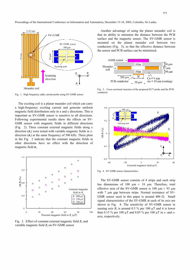
Fig. 1 shows the structure of the proposed high-frequency ECT probe designed for this experiment. It consists of an exciting coil and a SV-GMR sensor.
Giant Magnetoresistance Based Eddy-Current Sensor for High-Speed PCB Defect Detection
Ravindra Koggalage, K. Chomsuwan, S. Yamada, M. Iwahara , and Udantha R. Abeyratne* Institute of Nature and Environmental Technology
Kanazawa University, 2-40-20 Kodatsuno, Kanazawa 920-8667, Ishikawa, Japan Email: [email protected]
*School of Information Technology and Electrical Engineering The University of Queensland, St Lucia, Brisbane, QLD4072, Australia
170
Proceedings of the International Conference on Information and Automation, December 15-18, 2005, Colombo, Sri Lanka.
Fig. 1. High frequency eddy current probe using SV-GMR sensor
The exciting coil is a planar meander coil which can carry
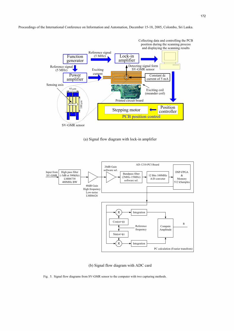
a high-frequency exciting current and generate uniform magnetic field distribution only in x and y directions. This is important as SV-GMR sensor is sensitive to all directions. Following experimental results show the effects on SV-GMR sensor with magnetic fields in different directions (Fig. 2). Three constant external magnetic fields along x direction (Bx) were tested with variable magnetic fields in z-direction (Bz) at the same frequency of 500 kHz. Three plots in the Fig. 2 indicate that the constant magnetic fields in other directions have no effect with the detection of magnetic field Bz.
Fig. 2. Effect of constant external magnetic field Bx and variable magnetic field Bz on SV-GMR sensor
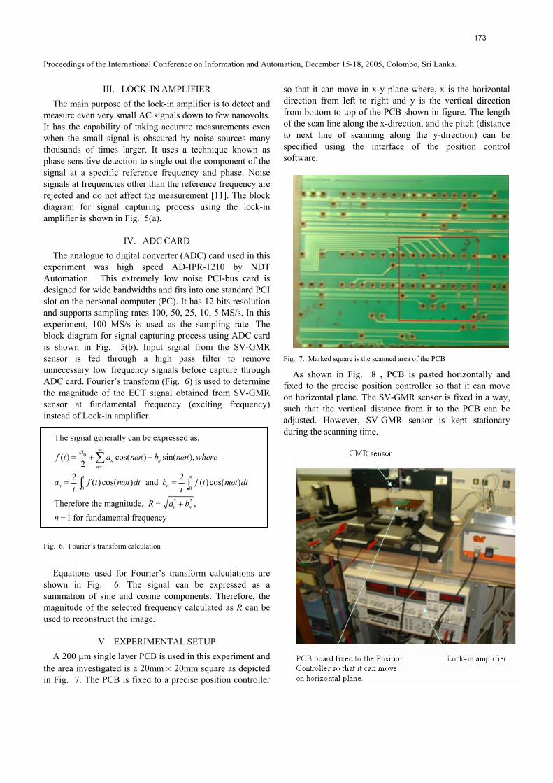
Another advantage of using the planer meander coil is that its ability to minimize the distance between the PCB surface and the magnetic sensor. The SV-GMR sensor is mounted on the planar meander coil between two conductors (Fig. 3), so that the effective distance between the sensor and PCB surface can be minimized.
Fig. 3. Cross-sectional structure of the proposed ECT probe and the PCB conductor
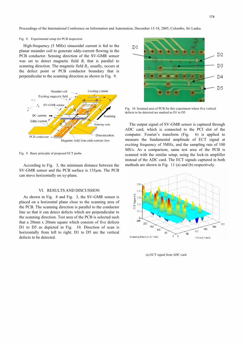
Fig. 4. SV-GMR sensor characteristics
The SV-GMR sensor consists of 4 strips and each strip
has dimensions of 100 µm × 18 µm. Therefore, total effective area of the SV-GMR sensor is 100 µm × 93 µm with 7 µm gap between strips. Normal resistance of SV-GMR sensor used in this paper is around 400 Ω. Small signal characteristics of the SV-GMR at each of its axis are shown in Fig. 4. The sensitivity of SV-GMR sensor in sensing axis Bz is around 0.5 % per 100 µT and it is lower than 0.15 % per 100 µT and 0.05 % per 100 µT in x- and y-axis, respectively.
171
Proceedings of the International Conference on Information and Automation, December 15-18, 2005, Colombo, Sri Lanka.
Poweramplifier
Functiongenerator
Lock-inamplifier
Excitingcurrent
Reference signal(5 MHz)
Reference signal(5 MHz)
Detecting signal formSV-GMR sensor
Collecting data and controlling the PCBposition during the scanning processand displaying the scanning results
Constant dccurrent of 5 mA
Printed circuit board
SV-GMR sensor
Exciting coil(meander coil)
Sensing axis
Stepping motor Positioncontroller
PCB position control
100 µm
93 µm
(a) Signal flow diagram with lock-in amplifier
High pass filter(-3dB at 500kHz)
LMH6738400MHz BW
Input fromSV-GMR
X
X
Sin(ωt+φ)
Cos(ωt+φ)
Integration
Integration
Referencefrequency
ComputeAmplitude
R
Bandpass filter(2MHz-15MHz)
software sel.
12 Bits 100MHzA/D conveter
DSP-FPGA&
Memory512 kSamples
AD-1210-PCI Board
PC calculation (Fourier transfrom)
20dB Gainsoftware sel.
40dB GainHigh frequency
Low-noiseLMH6626
(b) Signal flow diagram with ADC card
Fig. 5. Signal flow diagrams from SV-GMR sensor to the computer with two capturing methods.
172
Proceedings of the International Conference on Information and Automation, December 15-18, 2005, Colombo, Sri Lanka.
III. LOCK-IN AMPLIFIER The main purpose of the lock-in amplifier is to detect and
measure even very small AC signals down to few nanovolts. It has the capability of taking accurate measurements even when the small signal is obscured by noise sources many thousands of times larger. It uses a technique known as phase sensitive detection to single out the component of the signal at a specific reference frequency and phase. Noise signals at frequencies other than the reference frequency are rejected and do not affect the measurement [11]. The block diagram for signal capturing process using the lock-in amplifier is shown in Fig. 5(a).
IV. ADC CARD The analogue to digital converter (ADC) card used in this
experiment was high speed AD-IPR-1210 by NDT Automation. This extremely low noise PCI-bus card is designed for wide bandwidths and fits into one standard PCI slot on the personal computer (PC). It has 12 bits resolution and supports sampling rates 100, 50, 25, 10, 5 MS/s. In this experiment, 100 MS/s is used as the sampling rate. The block diagram for signal capturing process using ADC card is shown in Fig. 5(b). Input signal from the SV-GMR sensor is fed through a high pass filter to remove unnecessary low frequency signals before capture through ADC card. Fourier’s transform (Fig. 6) is used to determine the magnitude of the ECT signal obtained from SV-GMR sensor at fundamental frequency (exciting frequency) instead of Lock-in amplifier.
0
1
0 0
2 2
The signal generally can be expressed as,
( ) cos( ) sin( ),2
2 2( ) cos( ) and ( ) cos( )
Therefore the magnitude, , 1 for fundamental frequency
n nn
t t
n n
n n
af t a n t b n t where
a f t n t dt b f t n t dtt t
R a bn
ω ω
ω ω
∞
=
= + +
= =
= +
=
∑
∫ ∫
Fig. 6. Fourier’s transform calculation
Equations used for Fourier’s transform calculations are
shown in Fig. 6. The signal can be expressed as a summation of sine and cosine components. Therefore, the magnitude of the selected frequency calculated as R can be used to reconstruct the image.
V. EXPERIMENTAL SETUP A 200 µm single layer PCB is used in this experiment and
the area investigated is a 20mm × 20mm square as depicted in Fig. 7. The PCB is fixed to a precise position controller
so that it can move in x-y plane where, x is the horizontal direction from left to right and y is the vertical direction from bottom to top of the PCB shown in figure. The length of the scan line along the x-direction, and the pitch (distance to next line of scanning along the y-direction) can be specified using the interface of the position control software.
Fig. 7. Marked square is the scanned area of the PCB
As shown in Fig. 8 , PCB is pasted horizontally and fixed to the precise position controller so that it can move on horizontal plane. The SV-GMR sensor is fixed in a way, such that the vertical distance from it to the PCB can be adjusted. However, SV-GMR sensor is kept stationary during the scanning time.
173
Proceedings of the International Conference on Information and Automation, December 15-18, 2005, Colombo, Sri Lanka.
Fig. 8. Experimental setup for PCB inspection
High-frequency (5 MHz) sinusoidal current is fed to the planar meander coil to generate eddy-current flowing in the PCB conductor. Sensing direction of the SV-GMR sensor was set to detect magnetic field Bz that is parallel to scanning direction. The magnetic field Bz, usually, occurs at the defect point or PCB conductor boundary that is perpendicular to the scanning direction as shown in Fig. 9.
Fig. 9. Basic principle of proposed ECT probe
According to Fig. 3, the minimum distance between the
SV-GMR sensor and the PCB surface is 135µm. The PCB can move horizontally on xy-plane.
VI. RESULTS AND DISCUSSION As shown in Fig. 8 and Fig. 3, the SV-GMR sensor is
placed on a horizontal plane close to the scanning area of the PCB. The scanning direction is parallel to the conductor line so that it can detect defects which are perpendicular to the scanning direction. Test area of the PCB is selected such that a 20mm x 20mm square which consists of five defects D1 to D5 as depicted in Fig. 10. Direction of scan is horizontally from left to right. D1 to D5 are the vertical defects to be detected.
Fig. 10. Scanned area of PCB for this experiment where five vertical defects to be detected are marked as D1 to D5.
The output signal of SV-GMR sensor is captured through
ADC card, which is connected to the PCI slot of the computer. Fourier’s transform (Fig. 6) is applied to measure the fundamental amplitude of ECT signal at exciting frequency of 5MHz, and the sampling rate of 100 MS/s. As a comparison, same test area of the PCB is scanned with the similar setup, using the lock-in amplifier instead of the ADC card. The ECT signals captured in both methods are shown in Fig. 11 (a) and (b) respectively.
(a) ECT signal from ADC card
174
Proceedings of the International Conference on Information and Automation, December 15-18, 2005, Colombo, Sri Lanka.
(b) ECT signal from Lock-in amplifier
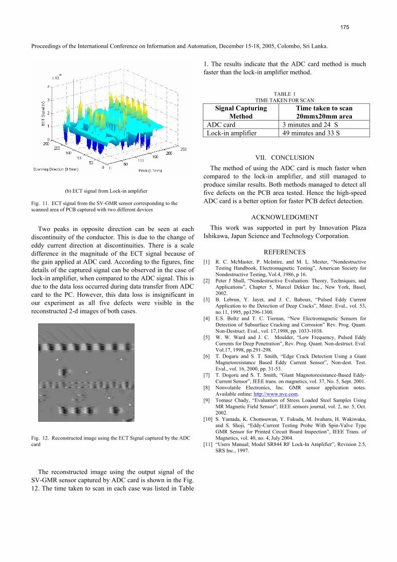
Fig. 11. ECT signal from the SV-GMR sensor corresponding to the scanned area of PCB captured with two different devices
Two peaks in opposite direction can be seen at each
discontinuity of the conductor. This is due to the change of eddy current direction at discontinuities. There is a scale difference in the magnitude of the ECT signal because of the gain applied at ADC card. According to the figures, fine details of the captured signal can be observed in the case of lock-in amplifier, when compared to the ADC signal. This is due to the data loss occurred during data transfer from ADC card to the PC. However, this data loss is insignificant in our experiment as all five defects were visible in the reconstructed 2-d images of both cases.
Fig. 12. Reconstructed image using the ECT Signal captured by the ADC card
The reconstructed image using the output signal of the
SV-GMR sensor captured by ADC card is shown in the Fig. 12. The time taken to scan in each case was listed in Table
1. The results indicate that the ADC card method is much faster than the lock-in amplifier method.
TABLE 1 TIME TAKEN FOR SCAN
VII. CONCLUSION The method of using the ADC card is much faster when
compared to the lock-in amplifier, and still managed to produce similar results. Both methods managed to detect all five defects on the PCB area tested. Hence the high-speed ADC card is a better option for faster PCB defect detection.
ACKNOWLEDGMENT This work was supported in part by Innovation Plaza
Ishikawa, Japan Science and Technology Corporation.
REFERENCES [1] R. C. McMaster, P. McIntire, and M. L. Mester, “Nondestructive
Testing Handbook, Electromagnetic Testing”, American Society for Nondestructive Testing, Vol.4, 1986, p 16.
[2] Peter J Shull, “Nondestructive Evaluation: Theory, Techniques, and Applications”, Chapter 5, Marcel Dekker Inc., New York, Basel, 2002.
[3] B. Lebrun, Y. Jayet, and J. C. Baboux, “Pulsed Eddy Current Application to the Detection of Deep Cracks”, Mater. Eval., vol. 53, no.11, 1995, pp1296-1300.
[4] E.S. Boltz and T. C. Tiernan, “New Electromagnetic Sensors for Detection of Subsurface Cracking and Corrosion” Rev. Prog. Quant. Non-Destruct. Eval., vol. 17,1998, pp. 1033-1038.
[5] W. W. Ward and J. C. Moulder, “Low Frequency, Pulsed Eddy Currents for Deep Penetration”, Rev. Prog. Quant. Non-destruct. Eval. Vol.17, 1998, pp.291-298.
[6] T. Dogaru and S. T. Smith, “Edge Crack Detection Using a Giant Magnetoresistance Based Eddy Current Sensor”, Non-dest. Test. Eval., vol. 16, 2000, pp. 31-53.
[7] T. Dogoru and S. T. Smith, “Giant Magnotoresistance-Based Eddy-Current Sensor”, IEEE trans. on magnetics, vol. 37, No. 5, Sept. 2001.
[8] Nonvolatile Electronics, Inc. GMR sensor application notes. Available online: http://www.nve.com.
[9] Tomasz Chady, “Evaluation of Stress Loaded Steel Samples Using MR Magnetic Field Sensor”, IEEE sensors journal, vol. 2, no. 5, Oct. 2002.
[10] S. Yamada, K. Chomsuwan, Y. Fukuda, M. Iwahara, H. Wakiwaka, and S. Shoji, “Eddy-Current Testing Probe With Spin-Valve Type GMR Sensor for Printed Circuit Board Inspection”, IEEE Trans. of Magnetics, vol. 40, no. 4, July 2004.
[11] “Users Manual; Model SR844 RF Lock-In Amplifier”, Revision 2.5, SRS Inc., 1997.
Signal Capturing Method
Time taken to scan 20mmx20mm area
ADC card 3 minutes and 24 S Lock-in amplifier 49 minutes and 33 S
175