Embed Size (px)
DESCRIPTION
report
Citation preview
This article has been accepted for inclusion in a future issue of this journal. Content is final as presented, with the exception of pagination.
IEEE TRANSACTIONS ON VERY LARGE SCALE INTEGRATION (VLSI) SYSTEMS 1
Design of Self-Timed Reconfigurable Controllersfor Parallel Synchronization via Wagging
James S. Guido, Graduate Student Member, IEEE, and Alexandre Yakovlev, Senior Member, IEEE
Abstract— Synchronization is an important issue in modernsystem design as systems-on-chips integrate more diverse tech-nologies, operating voltages, and clock frequencies on a singlesubstrate. This paper presents a methodology for the designand implementation of a self-timed reconfigurable control devicesuitable for a parallel cascaded flip-flop synchronizer basedon a principle known as wagging, through the applicationof distributed feedback graphs. By modifying the endpointadjacency of a common behavior graph via one-hot codes,several configurable modes can be implemented in a singledesign specification, thereby facilitating direct control over thesynchronization time and the mean-time between failures ofthe parallel master-slave latches in the synchronizer. Therefore,the resulting implementation is resistant to process nonidealities,which are present in physical design layouts. This paper includesa discussion of the reconfiguration protocol, and implementationsof both a sequential token ring control device, and an interruptsubsystem necessary for reconfiguration, all simulated in UMC90-nm technology. The interrupt subsystem demonstrates oper-ating frequencies between 505 and 818 MHz per module, withaverage power consumptions between 70.7 and 90.0 µW in thetypical-typical case under a corner analysis.
Index Terms— Asynchronous, combinational, controllers, digi-tal circuit design, reconfigurable, self-timed, sequential, synchro-nization.
I. INTRODUCTION
AS TECHNOLOGY trends lead modern systems-on-chips(SoCs) to incorporate designs of increasing complexity,
the reliable transmission of data items across a chip remainsan issue of paramount concern. It becomes difficult to designa single global clock that is capable of regulating data transac-tions throughout the system, due to the large number of designconstraints required to guarantee reliable operation [1]. In thepresence of multiple (possibly dynamic) voltage and frequencyoperating points, the single clock paradigm becomes even lesstractable as a design solution. It is simpler to construct a SoCwith several different voltage/frequency islands (each withtheir own local clock) and then synchronize the data itemsbetween the regions. This principle forms the basis of theglobally asynchronous locally synchronous (GALS) signalingparadigm. GALS requires the presence of an asynchronouswrapper to reliably pass data between the two clock regions,
Manuscript received January 25, 2013; revised July 16, 2013 andNovember 22, 2013; accepted January 16, 2014. This work was supported bythe EPSRC for Globally Asynchronous Elastic Logic Synthesis under GrantEP/I038551/1.
The authors are with the Department of Electrical and Electronic Engi-neering, University of Newcastle, Newcastle NE1 7RU, U.K. (e-mail:[email protected]; [email protected]).
Digital Object Identifier 10.1109/TVLSI.2014.2306176
which must then be synchronized at each end of the trans-fer [2]. Another related concept known as a networks-on-chip (NoC) accomplishes a similar purpose by transmittingdata items as packets along the wires of a homogenousinterconnection network [3]. In a NoC, synchronization isrequired at the endpoints of the network interface [4]. In bothcases, the design constraints of the clock distribution networkin SoCs, which incorporate either GALS or NoCs are easier tosatisfy, though a full discussion of both are beyond the scopeof this paper. As synchronization is required at some juncturein SoCs incorporating either GALS or a NoC, it serves toillustrate that synchronization remains a relevant issue in thedesign of modern digital systems.
The synchronizer circuits present in the network interfaceof a NoC serve as a useful example for the purposes of thisintroduction. Several approaches exist for constructing syn-chronizer circuits suitable for such an interface, each with ben-efits and tradeoffs. The relevant synchronizer circuit designsof interest are based on cascaded master-slave flip-flops, withthe key points of difference being whether or not the circuitsincorporate a first-in first-out (FIFO) buffer, and/or a (possiblyvariable) number of parallel master-slave flip-flops [5]–[7].
In a basic cascaded flip-flop synchronizer (incorporatingneither a FIFO nor parallelism), synchronization is performedusing two or more flip-flops in a master-slave configuration ateach end of a transmitter/receiver (Tx/Rx) device pair. Whenthe master device is transparent, the slave is opaque, and viceversa. Voltages in the master latch may be indeterminate whenthe latch becomes opaque and the signal is sampled, however,the value must be resolved to a clear logical high or logicallow value by the time the slave device becomes opaque andthe master latch once again becomes transparent. Sadly, thethroughput of data are governed by the roundtrip delay throughthe transmitter and receiver ends of the synchronizer, whichincreases with the number of serial flip-flop elements in thechain [5]. Fortunately, incorporating a FIFO buffer into theTx/Rx pair decouples the reading and writing operations fromeach other, allowing both operations to be done as soon asthe system is ready [5]. The read operation can take place aslong as there is valid data stored in the FIFO, while the writeoperation can be performed as long as the FIFO has spaceavailable in the buffer. However, the FIFO will incur penaltiesdue to overflow/underflow if the sender and receiver clocksare not well matched [6].
To further exacerbate the problem, instances of synchroniza-tion failures (i.e., when the voltages in the master-slave flip-flops of a synchronizer fail to resolve within an allotted time)are increased in modern technologies due to both increased
1063-8210 © 2014 IEEE. Translations and content mining are permitted for academic research only. Personal use is also permitted,but republication/redistribution requires IEEE permission. See http://www.ieee.org/publications_standards/publications/rights/index.html for more information.
This article has been accepted for inclusion in a future issue of this journal. Content is final as presented, with the exception of pagination.
2 IEEE TRANSACTIONS ON VERY LARGE SCALE INTEGRATION (VLSI) SYSTEMS
data rates, and reduced voltages [8]. While many solutionsexist to resolve the issues of data synchronization, the solutionswhich employ parallelism (i.e., using many components toperform one specific task) remain of particular interest to thispaper. Employing parallelism in the context of a synchronizercircuit has two useful properties.
1) With appropriate scheduling of parallel tasks, mis-matches between the transmitter and receiver ends ofa synchronizer can be minimized.
2) The mean-time between synchronization failures(MTBF) can be manipulated by adjusting the degree ofparallelism employed.
These two properties have appeared in other bodies of lit-erature in one form or another. Of specific interest is priorwork by van Berkel [9], on handshaking circuits wherehe defined a concept known as wagging (i.e., employingparallelism, in tandem with the scheduling of tasks viatime division). Ebergen [10] also experimented with thescheduling of tasks in parallel compositions of finite statemachines in his own work. More recently, Brej [11] usedthe concept of wagging to compose a system of parallellogic wherein he used the phrase wagging level to denotethe number of data copies in his system. Each copy wasthen given a unique slice and slice number to schedule itstasks.
On the topic of parallel synchronizer circuits, Jex andDike [7] put forth the idea of using parallel interconnectsto increase the throughput and metastability characteristics ofa synchronizer circuit. Alshaikh et al. [12], also presented asynchronizer design which employed wagging. However, priorliterature on parallel synchronizer circuits remains deficient ontwo key points.
1) Prior controller designs have been static in nature. Themanipulation of the MTBF in parallel synchronizercircuits via the process of reconfiguration has remainedunexplored.
2) The construction of a sequential token ring con-troller suitable for such a task has also remainedobscure.
To that end, this paper presents a brief overview of a parallelsynchronizer design based on the principles of wagging, andthen uses that framework to specify a reconfigurable controllerbased on sequential logic and embedded graphs, which is suit-able for the manipulation of the same. This paper is organizedas follows. Section II presents an overview of the waggingprinciple as well as its applications to the design of synchro-nizers, along with the top-level architecture of the controllerdesign. Section III presents the theoretical underpinnings ofa reconfigurable control device based on token shifting andtargeted for use in parallel synchronizers will be presented.A comparison of the benefits and tradeoffs of various tokenring designs will be discussed in Section IV, along with apresentation of some experimental results. Section V willgive similar treatment to the interrupt subsystem. Finally,conclusion will be drawn in Section VI concerning futureresearch directions.
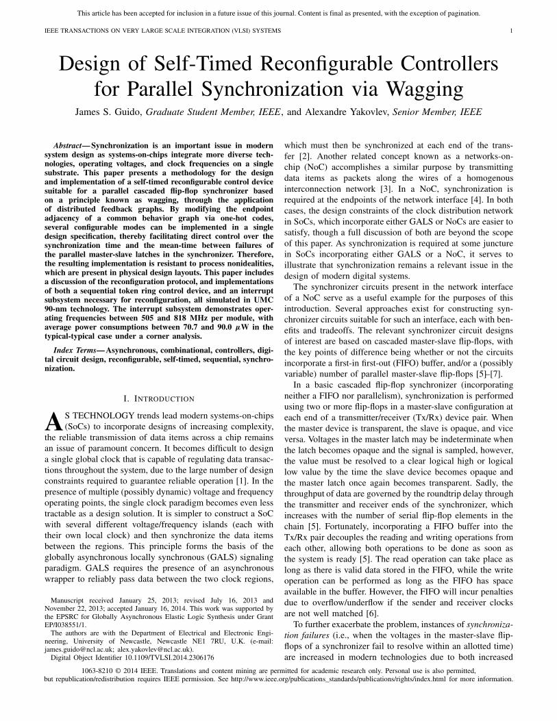
Fig. 1. Annotated diagram of a two-way wagging buffer.
II. WAGGING OVERVIEW
A design incorporating wagging will always contain twoproperties, regardless of whether or not the design is controlledvia synchronous control signals or asynchronous communica-tion signals called handshakes.
1) Usage of parallel components to share the workload ofa task.
2) Scheduling of said tasks via time division.
To understand the concept of wagging, we must look to priorliterature on the subject. In 1992, van Berkel [9] presentedwork on asynchronous handshaking circuits, including workon a two-way buffer, which he referred to as a wagging buffer,reproduced in Fig. 1. Active ports in Fig. 1 are represented byblack dots, while passive ports are indicated by white dots.
The data flow aspect of the buffer is comprised of mixers (|),transferrers (T ), and variables x , and y which function asmemory. Transferrers are components, which pass valuesthrough their active ports when triggered along their passiveports, while mixers are components which pass handshakesfrom their passive ports to their active ports, and can eitheract as demultiplexers (DEMUX) or multiplexers (MUX). Theoperation of the circuit is as follows.
1) x ← a @t1 (x is written with the value of a at timet1).
2) c← x (i.e., a @t1 is passed to the output of the buffer),and y← a @t2 (y gets the value of a at time t2).
3) c← y (i.e., a @t2), and x ← a @t3.
Step 1 only occurs at the startup of the circuit, to place validdata on x prior to its read out during the next step. Thereafter,only steps 2 and 3 are executed. Thus, even though x and yin Fig. 1 are placed in parallel, functionally they act as if theywere placed in series due to the scheduling of tasks [9].
A. Applications to Synchronizers
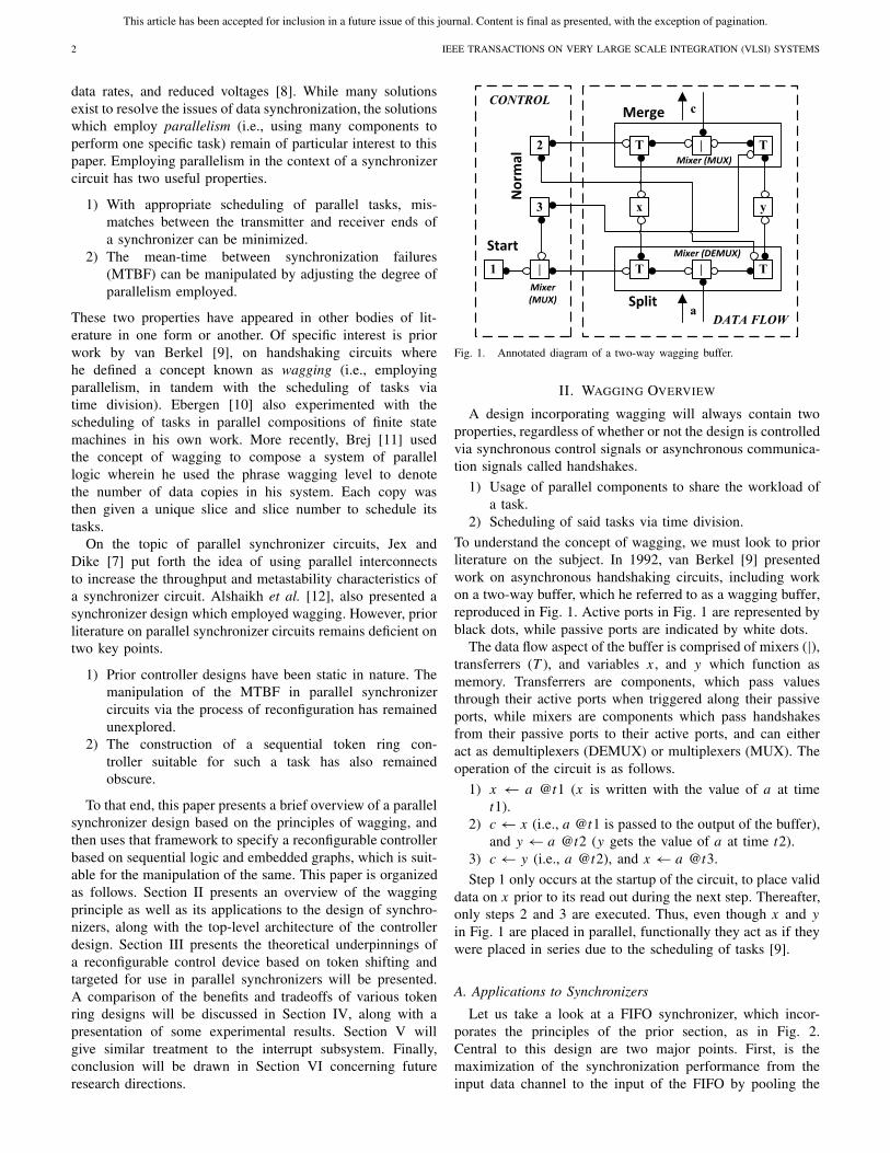
Let us take a look at a FIFO synchronizer, which incor-porates the principles of the prior section, as in Fig. 2.Central to this design are two major points. First, is themaximization of the synchronization performance from theinput data channel to the input of the FIFO by pooling the
This article has been accepted for inclusion in a future issue of this journal. Content is final as presented, with the exception of pagination.
GUIDO AND YAKOVLEV: DESIGN OF SELF-TIMED RECONFIGURABLE CONTROLLERS 3
Fig. 2. Top view of a FIFO synchronizer incorporating wagging at the transmitter and receiver.
gain-bandwidth products of the parallel master-slave flip-flops,as illustrated in [13]. Second is the manipulation of the dataflow mismatch between the transmitter (Tx) and receiver (Rx)ends of the synchronizer. As the focus of this paper centerson the construction of a control device used to schedule thetasks in the synchronizer from the input data channel to theinput of the FIFO, only the first point is relevant in this paper.A detailed study and analysis of the second point is left forfuture work, though Fig. 2 shows a general overview of theentire system.
First, let us assume the FIFO is asynchronous, and that readsand writes occur independently of each other, where fclk(Tx)
and fclk(Rx) represent the local data rates of the transmitterand receiver regions of the synchronizer, respectively. Let usfurther assume that i and j are the multiples of a commonbase frequency f0, and that i < j < 2i (i.e., the transmitter isfaster than the receiver, but not by more than a factor of 2).
With those assumptions in hand, we can step through theoperation of Fig. 2 as follows. The serial input data andwrite validation signals (DATA, WRITE) from the transmitterarrive at the splitter module at a rate of j × f0 where theyare both split into j identical signals using mixers. Thesesignals are then broken into j tasks (slices), through samplingvia the use of j parallel master-slave flip-flops which actas synchronization elements. Thereafter, these synchronizationelements are triggered using control signals, which all operateat a base frequency of f0, but are offset from each other by jdivisions, as shown in Fig. 3 (though only DATA are shown).Finally, the DATA and WRITE signals arrive at the FIFO inputin j parallel lines operating at rate of f0. Section II-B willillustrate the impact of this process on the synchronizer MTBF.
Continuing forward, we can now examine the operation ofthe synchronizer from the output of the FIFO to the inputof the receiver. Because i �= j , and i < j < 2i , the FIFOis still subjected to data accumulation. To minimize suchaccumulation, the receiver needs to be designed to allow forthe data being read out from the FIFO to temporarily exceed
the amount of data being written in when certain conditionsare met. This is accomplished by allowing the read operationsto be done either serially, or in parallel.
Both read operations can use the same hardware. During aserial read, i parallel data lines from the FIFO are sent to amixer that recombines them along dataprime at a rate of i× f0,in a manner, which is identical to the recombination of thesignals in the wagging buffer discussed earlier. A parallel readoperation functions similarly, except that data are simultane-ously read out along both dataprime and datasec.
Whether or not a serial or parallel data read is necessarydepends on the present memory differential between the trans-mitter and receiver ends of the FIFO synchronizer, ( j − i)curas defined by
If ( j − i)+∑
( j − i)cur < i, then increase∑
( j − i)cur by ( j − i), (serial read)
If ( j − i)+∑
( j − i)cur ≥ i, then decrease∑
( j − i)cur by i − ( j − i), (parallel read). (1)
When the conditions for a parallel read are met, the systemcontinues parallel read operations until the memory differentialreaches 0, whereafter it resumes serial operation. It shouldalso be noted that read acknowledgement signal is processedin vectors of length i or 2i depending on whether a serial orparallel read operation was last performed.
However, it is worth reiterating that the focus of this paper ison the design and implementation of the reconfigurable controldevice suitable for this architecture, and that the material abovemerely forms crucial context.
B. Impacts on Synchronizer MTBF
In general, the MTBF of a synchronizer is characterized interms of three parameters, τ , Tw, and �tin. �tin is definedas the region of vulnerability where concurrent transitions
This article has been accepted for inclusion in a future issue of this journal. Content is final as presented, with the exception of pagination.
4 IEEE TRANSACTIONS ON VERY LARGE SCALE INTEGRATION (VLSI) SYSTEMS
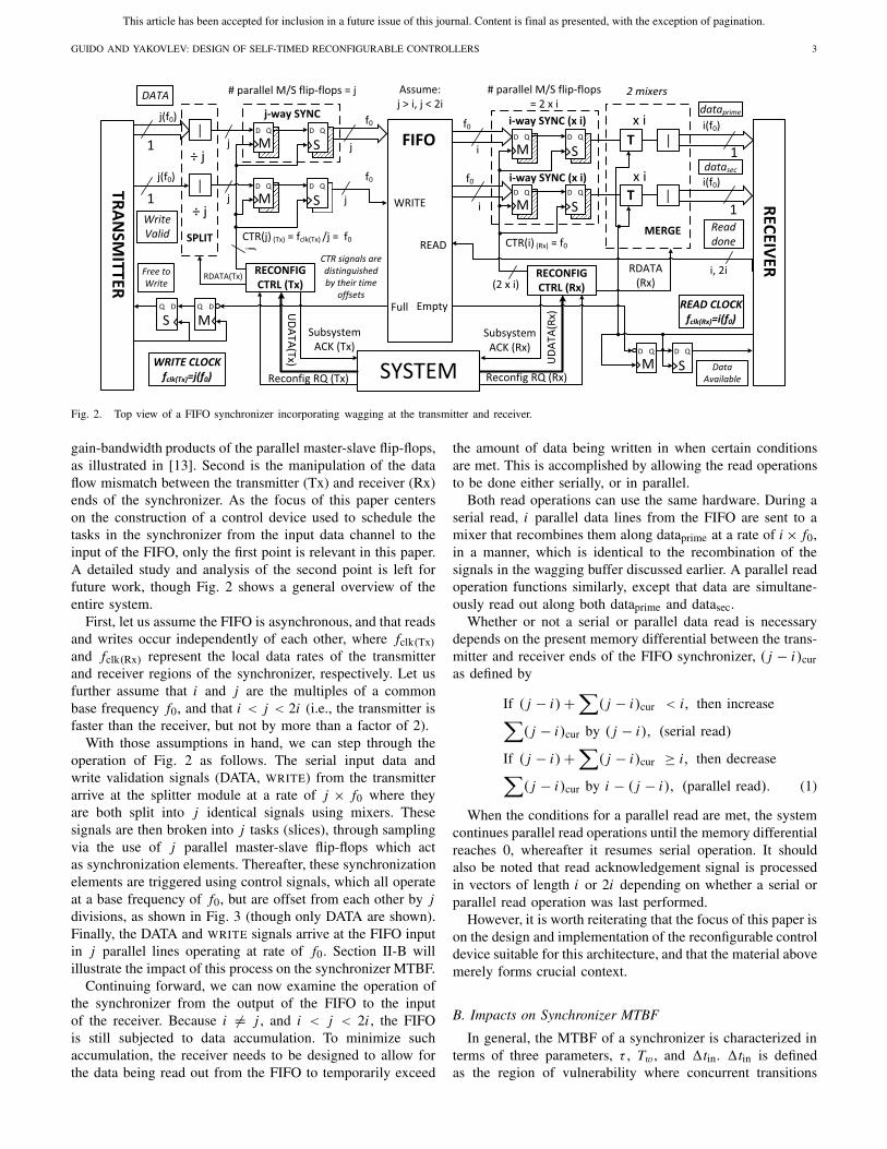
Fig. 3. Overview of wagging synchronization. (a) Data flow from the transmitter end of a wagging synchronizer to the input of the FIFO in Fig. 2 withj = 3 and a 50% duty cycle. (b) Top view of a reconfigurable controller suitable for a wagging synchronizer.
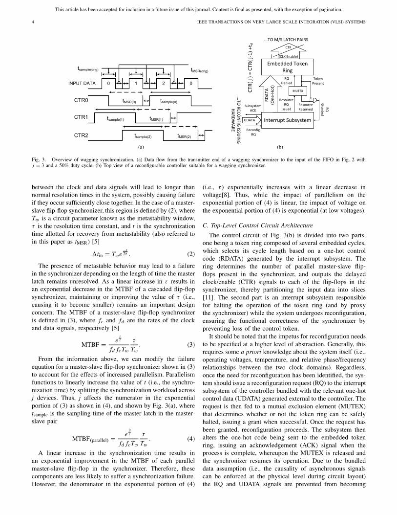
between the clock and data signals will lead to longer thannormal resolution times in the system, possibly causing failureif they occur sufficiently close together. In the case of a master-slave flip-flop synchronizer, this region is defined by (2), whereTw is a circuit parameter known as the metastability window,τ is the resolution time constant, and t is the synchronizationtime allotted for recovery from metastability (also referred toin this paper as tMSR) [5]
�tin = Twe−t2τ . (2)
The presence of metastable behavior may lead to a failurein the synchronizer depending on the length of time the masterlatch remains unresolved. As a linear increase in τ results inan exponential decrease in the MTBF of a cascaded flip-flopsynchronizer, maintaining or improving the value of τ (i.e.,causing it to become smaller) remains an important designconcern. The MTBF of a master-slave flip-flop synchronizeris defined in (3), where fc and fd are the rates of the clockand data signals, respectively [5]
MTBF = etτ
fd fcTw
τ
Tw. (3)
From the information above, we can modify the failureequation for a master-slave flip-flop synchronizer shown in (3)to account for the effects of increased parallelism. Parallelismfunctions to linearly increase the value of t (i.e., the synchro-nization time) by splitting the synchronization workload acrossj devices. Thus, j affects the numerator in the exponentialportion of (3) as shown in (4), and shown by Fig. 3(a), wheretsample is the sampling time of the master latch in the master-slave pair
MTBF(parallel) = ejtτ
fd fcTw
τ
Tw. (4)
A linear increase in the synchronization time results inan exponential improvement in the MTBF of each parallelmaster-slave flip-flop in the synchronizer. Therefore, thesecomponents are less likely to suffer a synchronization failure.However, the denominator in the exponential portion of (4)
(i.e., τ ) exponentially increases with a linear decrease involtage[8]. Thus, while the impact of parallelism on theexponential portion of (4) is linear, the impact of voltage onthe exponential portion of (4) is exponential (at low voltages).
C. Top-Level Control Circuit Architecture
The control circuit of Fig. 3(b) is divided into two parts,one being a token ring composed of several embedded cycles,which selects its cycle length based on a one-hot controlcode (RDATA) generated by the interrupt subsystem. Thering determines the number of parallel master-slave flip-flops present in the synchronizer, and outputs the delayedclock/enable (CTR) signals to each of the flip-flops in thesynchronizer, thereby partitioning the input data into slices[11]. The second part is an interrupt subsystem responsiblefor halting the operation of the token ring (and by proxythe synchronizer) while the system undergoes reconfiguration,ensuring the functional correctness of the synchronizer bypreventing loss of the control token.
It should be noted that the impetus for reconfiguration needsto be specified at a higher level of abstraction. Generally, thisrequires some a priori knowledge about the system itself (i.e.,operating voltages, temperature, and relative phase/frequencyrelationships between the two clock domains). Regardless,once the need for reconfiguration has been identified, the sys-tem should issue a reconfiguration request (RQ) to the interruptsubsystem of the controller bundled with the relevant one-hotcontrol data (UDATA) generated external to the controller. Therequest is then fed to a mutual exclusion element (MUTEX)that determines whether or not the token ring can be safelyhalted, issuing a grant when successful. Once the request hasbeen granted, reconfiguration proceeds. The subsystem thenalters the one-hot code being sent to the embedded tokenring, issuing an acknowledgement (ACK) signal when theprocess is complete, whereupon the MUTEX is released andthe synchronizer resumes its operation. Due to the bundleddata assumption (i.e., the causality of asynchronous signalscan be enforced at the physical level during circuit layout)the RQ and UDATA signals are prevented from becoming
This article has been accepted for inclusion in a future issue of this journal. Content is final as presented, with the exception of pagination.
GUIDO AND YAKOVLEV: DESIGN OF SELF-TIMED RECONFIGURABLE CONTROLLERS 5
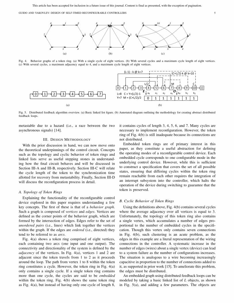
Fig. 4. Behavior graphs of a token ring. (a) With a single cycle of eight vertices. (b) With several cycles and a maximum cycle length of eight vertices.(c) With several cycles, a maximum adjacency equal to 4, and a maximum cycle length of eight vertices.
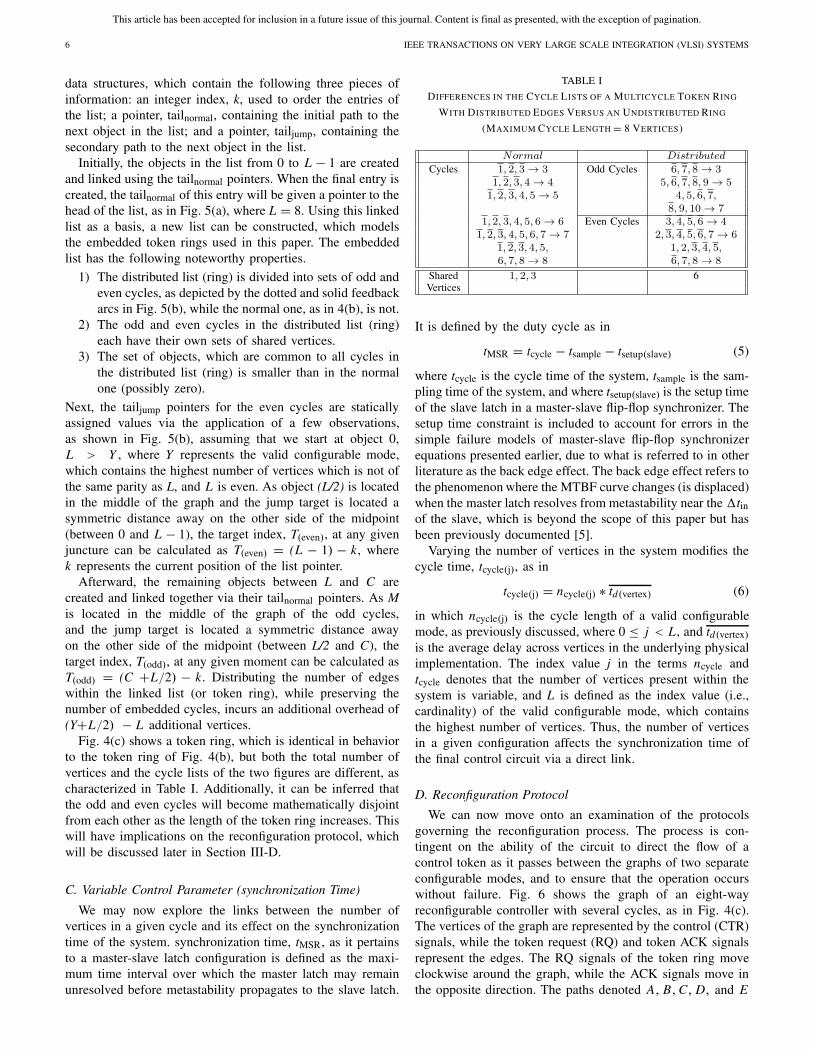
Fig. 5. Distributed feedback algorithm overview. (a) Basic linked list figure. (b) Annotated diagram outlining the methodology for creating abstract distributedfeedback loops.
metastable due to a hazard (i.e., a race between the twoasynchronous signals) [14].
III. DESIGN METHODOLOGY
With the prior discussion in hand, we can now move ontothe theoretical underpinnings of the control circuit. Conceptssuch as the topology and cyclic behavior of token rings andlinked lists serve as useful stepping stones in understand-ing how the final circuit behaves and will be discussed inSection III-A and III-B, respectively. Section III-C will relatethe cycle length of the token to the synchronization timeallotted for recovery from metastability. Finally, Section III-Dwill discuss the reconfiguration process in detail.
A. Topology of Token Rings
Explaining the functionality of the reconfigurable controldevice explored in this paper requires understanding a fewkey concepts. The first of these is that of a behavior graph.Such a graph is composed of vertices and edges. Vertices aredefined as the corner points of the behavior graph, which areformed by the intersection of edges. Edges refer to the set ofunordered pairs (i.e., lines) which link together the verticeswithin the graph. If the edges are ordered (i.e., directed) theytend to be referred to as arcs.
Fig. 4(a) shows a token ring comprised of eight vertices,each containing two arcs (one input and one output). Theconnectivity and directionality of the system is defined by theadjacency of the vertices. In Fig. 4(a), vertices 1 and 2 areadjacent since the token travels from 1 to 2 as it proceedsaround the loop. The path from vertex 1 to 8 within the tokenring constitutes a cycle. However, the token ring in Fig. 4(a)only contains a single cycle. If a single token ring containsmore than one cycle, the cycles are said to be embeddedwithin the token ring. Fig. 4(b) shows the same token ringas Fig. 4(a), but instead of having only one cycle of length 8,
it contains cycles of length 3, 4, 5, 6, and 7. Many cycles arenecessary to implement reconfiguration. However, the tokenring of Fig. 4(b) is still inadequate because its connections arenot distributed.
Embedded token rings are of primary interest in thispaper, as they constitute a useful abstraction for definingthe operating modes of a reconfigurable control device. Eachembedded cycle corresponds to one configurable mode in theunderlying control device. However, while this is sufficientto construct a specification that covers the set of all possiblestates, ensuring that differing cycles within the token ringremain reachable from each other requires the integration ofan interrupt subsystem into the controller, which halts theoperation of the device during switching to guarantee that thetoken is preserved.
B. Cyclic Behavior of Token Rings
Using the definitions above, Fig. 4(b) contains several cycleswhere the average adjacency over all vertices is equal to 3.Unfortunately, the topology of this token ring also containsa single vertex, which accumulates a number of edges pro-portional to the number of embedded cycles in the specifi-cation. Though this vertex only contains seven connectionsin Fig. 4(b), such clustering is an acute problem, as theedges in this example are a literal representation of the wiringconnections in the controller. A systematic increase in thenumber of edges (wires) about a single vertex (device) can leadto a system failure as the number of configurations increases.The situation is analogous to a wire becoming increasinglycapacitive in proportion to the number of connections added toit, as supported in prior work [15]. To ameliorate this problem,the edges must be distributed.
An embedded graph using distributed feedback loops can bemodeled by taking a basic linked list of L objects, as shownin Fig. 5(a), and adding a few parameters. The objects are
This article has been accepted for inclusion in a future issue of this journal. Content is final as presented, with the exception of pagination.
6 IEEE TRANSACTIONS ON VERY LARGE SCALE INTEGRATION (VLSI) SYSTEMS
data structures, which contain the following three pieces ofinformation: an integer index, k, used to order the entries ofthe list; a pointer, tailnormal, containing the initial path to thenext object in the list; and a pointer, tailjump, containing thesecondary path to the next object in the list.
Initially, the objects in the list from 0 to L − 1 are createdand linked using the tailnormal pointers. When the final entry iscreated, the tailnormal of this entry will be given a pointer to thehead of the list, as in Fig. 5(a), where L = 8. Using this linkedlist as a basis, a new list can be constructed, which modelsthe embedded token rings used in this paper. The embeddedlist has the following noteworthy properties.
1) The distributed list (ring) is divided into sets of odd andeven cycles, as depicted by the dotted and solid feedbackarcs in Fig. 5(b), while the normal one, as in 4(b), is not.
2) The odd and even cycles in the distributed list (ring)each have their own sets of shared vertices.
3) The set of objects, which are common to all cycles inthe distributed list (ring) is smaller than in the normalone (possibly zero).
Next, the tailjump pointers for the even cycles are staticallyassigned values via the application of a few observations,as shown in Fig. 5(b), assuming that we start at object 0,L > Y , where Y represents the valid configurable mode,which contains the highest number of vertices which is not ofthe same parity as L, and L is even. As object (L/2) is locatedin the middle of the graph and the jump target is located asymmetric distance away on the other side of the midpoint(between 0 and L − 1), the target index, T(even), at any givenjuncture can be calculated as T(even) = (L − 1) − k, wherek represents the current position of the list pointer.
Afterward, the remaining objects between L and C arecreated and linked together via their tailnormal pointers. As Mis located in the middle of the graph of the odd cycles,and the jump target is located a symmetric distance awayon the other side of the midpoint (between L/2 and C), thetarget index, T(odd), at any given moment can be calculated asT(odd) = (C +L/2) − k. Distributing the number of edgeswithin the linked list (or token ring), while preserving thenumber of embedded cycles, incurs an additional overhead of(Y+L/2) − L additional vertices.
Fig. 4(c) shows a token ring, which is identical in behaviorto the token ring of Fig. 4(b), but both the total number ofvertices and the cycle lists of the two figures are different, ascharacterized in Table I. Additionally, it can be inferred thatthe odd and even cycles will become mathematically disjointfrom each other as the length of the token ring increases. Thiswill have implications on the reconfiguration protocol, whichwill be discussed later in Section III-D.
C. Variable Control Parameter (synchronization Time)
We may now explore the links between the number ofvertices in a given cycle and its effect on the synchronizationtime of the system. synchronization time, tMSR, as it pertainsto a master-slave latch configuration is defined as the maxi-mum time interval over which the master latch may remainunresolved before metastability propagates to the slave latch.
TABLE I
DIFFERENCES IN THE CYCLE LISTS OF A MULTICYCLE TOKEN RING
WITH DISTRIBUTED EDGES VERSUS AN UNDISTRIBUTED RING
(MAXIMUM CYCLE LENGTH = 8 VERTICES)
It is defined by the duty cycle as in
tMSR = tcycle − tsample − tsetup(slave) (5)
where tcycle is the cycle time of the system, tsample is the sam-pling time of the system, and where tsetup(slave) is the setup timeof the slave latch in a master-slave flip-flop synchronizer. Thesetup time constraint is included to account for errors in thesimple failure models of master-slave flip-flop synchronizerequations presented earlier, due to what is referred to in otherliterature as the back edge effect. The back edge effect refers tothe phenomenon where the MTBF curve changes (is displaced)when the master latch resolves from metastability near the �tinof the slave, which is beyond the scope of this paper but hasbeen previously documented [5].
Varying the number of vertices in the system modifies thecycle time, tcycle(j), as in
tcycle(j) = ncycle(j) ∗ td(vertex) (6)
in which ncycle(j) is the cycle length of a valid configurablemode, as previously discussed, where 0 ≤ j < L, and td(vertex)
is the average delay across vertices in the underlying physicalimplementation. The index value j in the terms ncycle andtcycle denotes that the number of vertices present within thesystem is variable, and L is defined as the index value (i.e.,cardinality) of the valid configurable mode, which containsthe highest number of vertices. Thus, the number of verticesin a given configuration affects the synchronization time ofthe final control circuit via a direct link.
D. Reconfiguration Protocol
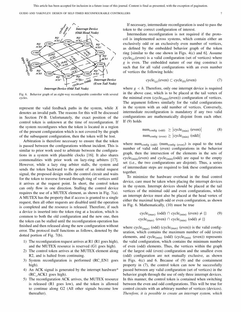
We can now move onto an examination of the protocolsgoverning the reconfiguration process. The process is con-tingent on the ability of the circuit to direct the flow of acontrol token as it passes between the graphs of two separateconfigurable modes, and to ensure that the operation occurswithout failure. Fig. 6 shows the graph of an eight-wayreconfigurable controller with several cycles, as in Fig. 4(c).The vertices of the graph are represented by the control (CTR)signals, while the token request (RQ) and token ACK signalsrepresent the edges. The RQ signals of the token ring moveclockwise around the graph, while the ACK signals move inthe opposite direction. The paths denoted A, B, C, D, and E
This article has been accepted for inclusion in a future issue of this journal. Content is final as presented, with the exception of pagination.
GUIDO AND YAKOVLEV: DESIGN OF SELF-TIMED RECONFIGURABLE CONTROLLERS 7
Fig. 6. Behavior graph of an eight-way reconfigurable controller with severalcycles.
represent the valid feedback paths in the system, while Xdenotes an invalid path. The reasons for this will be discussedin Section IV-B. Unfortunately, the exact position of thecontrol token is unknown at the time of reconfiguration. Ifthe system reconfigures when the token is located in a regionof the present configuration which is not covered by the graphof the subsequent configuration, then the token will be lost.
Arbitration is therefore necessary to ensure that the tokenis passed between the configurations without incident. This issimilar to prior work used to arbitrate between the configura-tions in a system with plausible clocks [16]. It also sharescommonalities with prior work on lazy-ring arbiters [17].However, while a lazy ring arbiter stalls, the system andsends the token backward to the point of an initial requestsignal, the proposed design stalls the control circuit and waitsfor the token to traverse forward through ring of vertices untilit arrives at the request point. In short, the control tokencan only flow in one direction. Stalling the control devicerequires the use of a MUTEX element, as shown in Fig. 7(a).A MUTEX has the property that if access is granted to a singlerequest, then all other requests are disabled until the operationis completed and the resource is released. Therefore, if sucha device is inserted into the token ring at a location, which iscommon to both the old configuration and the new one, thenthe token can be stalled until the reconfiguration operation hasfinished and then released along the new configuration withouterror. The protocol itself functions as follows, denoted by thedotted portion of Fig. 7(b).
1) The reconfiguration request arrives at R1 (R1 goes high),and the MUTEX resource is reserved (G1 goes high).
2) The control token arrives at the MUTEX element alongR2, and is halted from continuing.
3) System reconfiguration is performed (RC_EN1 goeshigh).
4) An ACK signal is generated by the interrupt hardware*(RC_ACK1 goes high).
5) The reconfiguration ACK arrives, the MUTEX resourceis released (R1 goes low), and the token is allowedto continue along G2 (All other signals become lowthereafter).
If necessary, intermediate reconfiguration is used to pass thetoken to the correct configuration of interest.
Intermediate reconfiguration is not required if the proto-col is implemented across systems, which contain either anexclusively odd or an exclusively even number of vertices,as defined by the embedded behavior graph of the tokenring [similar to the one shown in Figs. 4(c) and 6]. Assumecycle(g)(even) is a valid configuration (set of vertices) whereg is even. The embedded nature of our ring construct issuch that for all valid configurations with an even numberof vertices the following holds:
cycle(g)(even) ⊂ cycle(h)(even) (7)
where g < h. Therefore, only one interrupt device is requiredin the above case, which is to be placed at the tail vertex ofthe minimal even (cycle(min)(even)) configuration of vertices.The argument follows similarly for the valid configurationsin the system with an odd number of vertices. Conversely,intermediate reconfiguration is mandatory if any two validconfigurations are mathematically disjoint from each other.If (9) holds
numconfig (odd) ≥∣∣cycle(min) (even)
∣∣ (8)
numconfig (even) ≥∣∣cycle(min) (odd)
∣∣
where numconfig (odd) (numconfig (even)) is equal to the totalnumber of valid odd (even) configurations in the behaviorgraph, then the intersection of the elements in the sets ofcycle(min)(even) and cycle(min)(odd) are equal to the emptyset (i.e., the two configurations are disjoint). Thus, a seriesof intermediate steps are required to link these configurationstogether.
To minimize the hardware overhead in the final controldevice, care must be taken when placing the interrupt devicesin the system. Interrupt devices should be placed at the tailvertices of the minimal odd and even configurations, whilean interrupt device must also be placed at the head vertex ofeither the maximal length odd or even configuration, as shownin Fig. 6. Mathematically, (10) must be true
cycle(max) (odd) ∩ cycle(min) (even) �= {} (9)
cycle(max) (even) ∩ cycle(min) (odd) �= {}where cycle(max) (odd) (cycle(max) (even)) is the valid config-uration, which contains the maximum number of odd (even)elements, and cycle(min) (odd) (cycle(min) (even)) representsthe valid configuration, which contains the minimum numberof even (odd) elements. Thus, the vertices within the graphof the largest odd (even) configuration and the smallest even(odd) configuration are not mutually exclusive, as shownin Figs. 4(c) and 6. Because of (9) and the containmentproperty in (7), the control token can now be successfullypassed between any valid configuration (set of vertices) in thebehavior graph through the use of only three interrupt devices.In this manner, the control token is contained when switchingbetween the even and odd configurations. This will be true forcontrol circuits with an arbitrary number of vertices (devices).Therefore, it is possible to create an interrupt system, which
This article has been accepted for inclusion in a future issue of this journal. Content is final as presented, with the exception of pagination.
8 IEEE TRANSACTIONS ON VERY LARGE SCALE INTEGRATION (VLSI) SYSTEMS
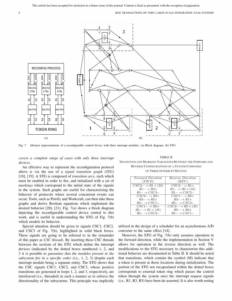
Fig. 7. Abstract representations of a reconfigurable control device with three interrupt modules. (a) Block diagram. (b) STG.
covers a complete range of cases with only three interruptdevices.
An effective way to represent the reconfiguration protocolabove is via the use of a signal transition graph (STG)[18], [19]. A STG is composed of transition arcs, each whichmust be enabled in order to fire, and initialized with a set ofmarkings which correspond to the initial state of the signalsin the system. Such graphs are useful for characterizing thebehavior of protocols where several concurrent events canoccur. Tools, such as Petrify and Workcraft, can then take thesegraphs and derive Boolean equations which implement thedesired behavior [20], [21]. Fig. 7(a) shows a block diagramdepicting the reconfigurable control device central to thiswork, and is useful in understanding the STG of Fig. 7(b)which models its behavior.
Special attention should be given to signals CSC1, CSC2,and CSC3 of Fig. 7(b), highlighted in solid black boxes.These signals are going to be referred to in the remainderof this paper as CSC threads. By inserting these CSC threadsbetween the sections of the STG which define the interruptdevices (indicated by the dotted boxes numbered 1, 2, and3 it is possible to guarantee that the modules present in thesubsystem fire in a specific order (i.e., 1, 2, 3) despite eachinterrupt module being a separate entity. The STG shows thatthe CSC signals CSC1, CSC2, and CSC3, whose positivetransitions are generated in loops 1, 2, and 3, respectively, areinterleaved (i.e., threaded) in such a manner as to enforce thedirectionality of the subsystems. This principle was implicitly
TABLE II
TRANSITION AND MARKING VARIATIONS BETWEEN THE FORWARD AND
REVERSE CONFIGURATIONS OF A SYSTEM COMPOSED
OF THREE INTERRUPT DEVICES
utilized in the design of a scheduler for an asynchronous A/Dconverter to the same effect [14].
However, the STG of Fig. 7(b) only assumes operation inthe forward direction, while the implementation in Section Vallows for operation in the reverse direction as well. Themodifications to the STG necessary to characterize this addi-tional behavior are documented in Table II. It should be notedthat transitions, which contain the symbol (M) indicate thata token is present at those locations during initialization. Theportion of the STG not encapsulated within the dotted boxescorresponds to external token ring which passes the controltoken through the system once the interrupt request signals(i.e., R1, R3, R5) have been de-asserted. It is also worth noting
This article has been accepted for inclusion in a future issue of this journal. Content is final as presented, with the exception of pagination.
GUIDO AND YAKOVLEV: DESIGN OF SELF-TIMED RECONFIGURABLE CONTROLLERS 9
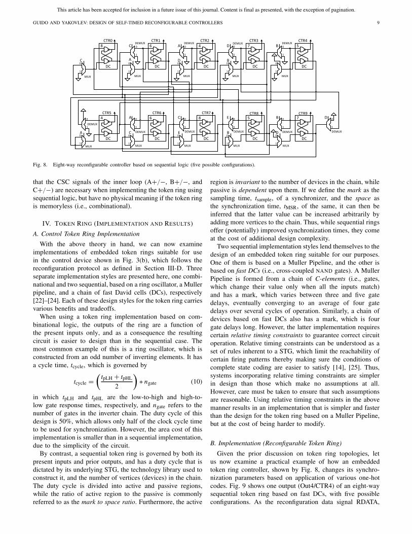
Fig. 8. Eight-way reconfigurable controller based on sequential logic (five possible configurations).
that the CSC signals of the inner loop (A+/−, B+/−, andC+/−) are necessary when implementing the token ring usingsequential logic, but have no physical meaning if the token ringis memoryless (i.e., combinational).
IV. TOKEN RING (IMPLEMENTATION AND RESULTS)
A. Control Token Ring Implementation
With the above theory in hand, we can now examineimplementations of embedded token rings suitable for usein the control device shown in Fig. 3(b), which follows thereconfiguration protocol as defined in Section III-D. Threeseparate implementation styles are presented here, one combi-national and two sequential, based on a ring oscillator, a Mullerpipeline, and a chain of fast David cells (DCs), respectively[22]–[24]. Each of these design styles for the token ring carriesvarious benefits and tradeoffs.
When using a token ring implementation based on com-binational logic, the outputs of the ring are a function ofthe present inputs only, and as a consequence the resultingcircuit is easier to design than in the sequential case. Themost common example of this is a ring oscillator, which isconstructed from an odd number of inverting elements. It hasa cycle time, tcycle, which is governed by
tcycle =(
tpLH + tpHL
2
)∗ ngate (10)
in which tpLH and tpHL are the low-to-high and high-to-low gate response times, respectively, and ngate refers to thenumber of gates in the inverter chain. The duty cycle of thisdesign is 50%, which allows only half of the clock cycle timeto be used for synchronization. However, the area cost of thisimplementation is smaller than in a sequential implementation,due to the simplicity of the circuit.
By contrast, a sequential token ring is governed by both itspresent inputs and prior outputs, and has a duty cycle that isdictated by its underlying STG, the technology library used toconstruct it, and the number of vertices (devices) in the chain.The duty cycle is divided into active and passive regions,while the ratio of active region to the passive is commonlyreferred to as the mark to space ratio. Furthermore, the active
region is invariant to the number of devices in the chain, whilepassive is dependent upon them. If we define the mark as thesampling time, tsample, of a synchronizer, and the space asthe synchronization time, tMSR, of the same, it can then beinferred that the latter value can be increased arbitrarily byadding more vertices to the chain. Thus, while sequential ringsoffer (potentially) improved synchronization times, they comeat the cost of additional design complexity.
Two sequential implementation styles lend themselves to thedesign of an embedded token ring suitable for our purposes.One of them is based on a Muller Pipeline, and the other isbased on fast DCs (i.e., cross-coupled NAND gates). A MullerPipeline is formed from a chain of C-elements (i.e., gates,which change their value only when all the inputs match)and has a mark, which varies between three and five gatedelays, eventually converging to an average of four gatedelays over several cycles of operation. Similarly, a chain ofdevices based on fast DCs also has a mark, which is fourgate delays long. However, the latter implementation requirescertain relative timing constraints to guarantee correct circuitoperation. Relative timing constraints can be understood as aset of rules inherent to a STG, which limit the reachability ofcertain firing patterns thereby making sure the conditions ofcomplete state coding are easier to satisfy [14], [25]. Thus,systems incorporating relative timing constraints are simplerin design than those which make no assumptions at all.However, care must be taken to ensure that such assumptionsare reasonable. Using relative timing constraints in the abovemanner results in an implementation that is simpler and fasterthan the design for the token ring based on a Muller Pipeline,but at the cost of being harder to modify.
B. Implementation (Reconfigurable Token Ring)
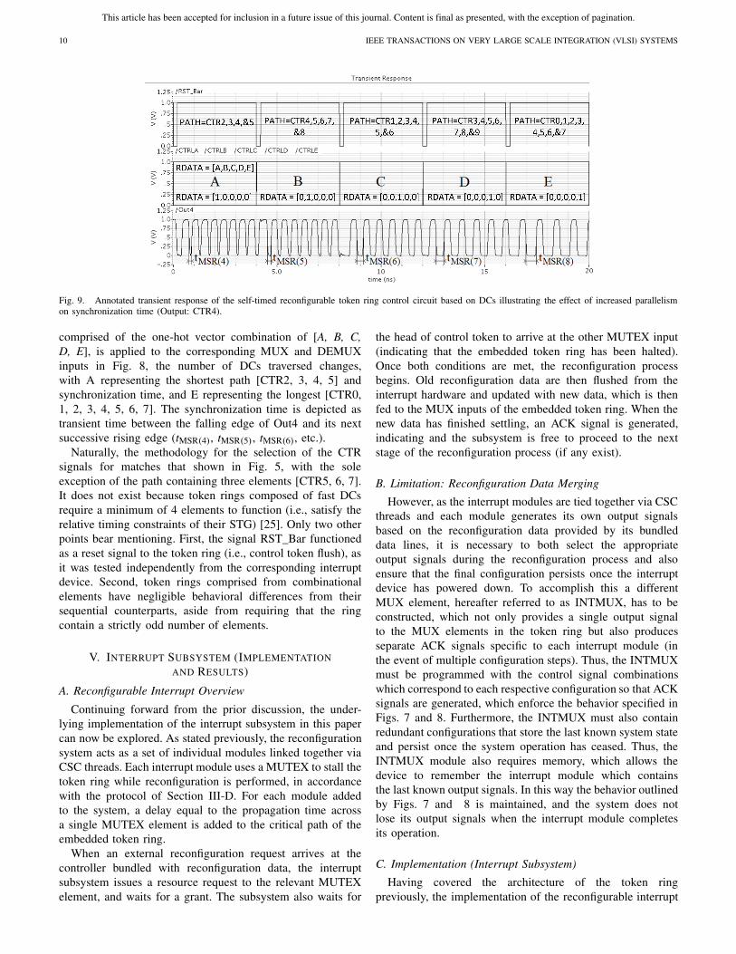
Given the prior discussion on token ring topologies, letus now examine a practical example of how an embeddedtoken ring controller, shown by Fig. 8, changes its synchro-nization parameters based on application of various one-hotcodes. Fig. 9 shows one output (Out4/CTR4) of an eight-waysequential token ring based on fast DCs, with five possibleconfigurations. As the reconfiguration data signal RDATA,
This article has been accepted for inclusion in a future issue of this journal. Content is final as presented, with the exception of pagination.
10 IEEE TRANSACTIONS ON VERY LARGE SCALE INTEGRATION (VLSI) SYSTEMS
Fig. 9. Annotated transient response of the self-timed reconfigurable token ring control circuit based on DCs illustrating the effect of increased parallelismon synchronization time (Output: CTR4).
comprised of the one-hot vector combination of [A, B, C,D, E], is applied to the corresponding MUX and DEMUXinputs in Fig. 8, the number of DCs traversed changes,with A representing the shortest path [CTR2, 3, 4, 5] andsynchronization time, and E representing the longest [CTR0,1, 2, 3, 4, 5, 6, 7]. The synchronization time is depicted astransient time between the falling edge of Out4 and its nextsuccessive rising edge (tMSR(4), tMSR(5), tMSR(6), etc.).
Naturally, the methodology for the selection of the CTRsignals for matches that shown in Fig. 5, with the soleexception of the path containing three elements [CTR5, 6, 7].It does not exist because token rings composed of fast DCsrequire a minimum of 4 elements to function (i.e., satisfy therelative timing constraints of their STG) [25]. Only two otherpoints bear mentioning. First, the signal RST_Bar functionedas a reset signal to the token ring (i.e., control token flush), asit was tested independently from the corresponding interruptdevice. Second, token rings comprised from combinationalelements have negligible behavioral differences from theirsequential counterparts, aside from requiring that the ringcontain a strictly odd number of elements.
V. INTERRUPT SUBSYSTEM (IMPLEMENTATION
AND RESULTS)
A. Reconfigurable Interrupt Overview
Continuing forward from the prior discussion, the under-lying implementation of the interrupt subsystem in this papercan now be explored. As stated previously, the reconfigurationsystem acts as a set of individual modules linked together viaCSC threads. Each interrupt module uses a MUTEX to stall thetoken ring while reconfiguration is performed, in accordancewith the protocol of Section III-D. For each module addedto the system, a delay equal to the propagation time acrossa single MUTEX element is added to the critical path of theembedded token ring.
When an external reconfiguration request arrives at thecontroller bundled with reconfiguration data, the interruptsubsystem issues a resource request to the relevant MUTEXelement, and waits for a grant. The subsystem also waits for
the head of control token to arrive at the other MUTEX input(indicating that the embedded token ring has been halted).Once both conditions are met, the reconfiguration processbegins. Old reconfiguration data are then flushed from theinterrupt hardware and updated with new data, which is thenfed to the MUX inputs of the embedded token ring. When thenew data has finished settling, an ACK signal is generated,indicating and the subsystem is free to proceed to the nextstage of the reconfiguration process (if any exist).
B. Limitation: Reconfiguration Data Merging
However, as the interrupt modules are tied together via CSCthreads and each module generates its own output signalsbased on the reconfiguration data provided by its bundleddata lines, it is necessary to both select the appropriateoutput signals during the reconfiguration process and alsoensure that the final configuration persists once the interruptdevice has powered down. To accomplish this a differentMUX element, hereafter referred to as INTMUX, has to beconstructed, which not only provides a single output signalto the MUX elements in the token ring but also producesseparate ACK signals specific to each interrupt module (inthe event of multiple configuration steps). Thus, the INTMUXmust be programmed with the control signal combinationswhich correspond to each respective configuration so that ACKsignals are generated, which enforce the behavior specified inFigs. 7 and 8. Furthermore, the INTMUX must also containredundant configurations that store the last known system stateand persist once the system operation has ceased. Thus, theINTMUX module also requires memory, which allows thedevice to remember the interrupt module which containsthe last known output signals. In this way the behavior outlinedby Figs. 7 and 8 is maintained, and the system does notlose its output signals when the interrupt module completesits operation.
C. Implementation (Interrupt Subsystem)
Having covered the architecture of the token ringpreviously, the implementation of the reconfigurable interrupt
This article has been accepted for inclusion in a future issue of this journal. Content is final as presented, with the exception of pagination.
GUIDO AND YAKOVLEV: DESIGN OF SELF-TIMED RECONFIGURABLE CONTROLLERS 11
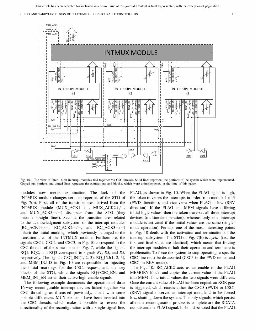
Fig. 10. Top view of three 16-bit interrupt modules tied together via CSC threads. Solid lines represent the portions of the system which were implemented.Grayed out portions and dotted lines represent the connections and blocks, which were unimplemented at the time of this paper.
modules now merits examination. The lack of theINTMUX module changes certain properties of the STG ofFig. 7(b). First, all of the transition arcs derived from theINTMUX module (MUX_ACK1+/−, MUX_ACK2+/−,and MUX_ACK3+/−) disappear from the STG (theybecome straight lines). Second, the transition arcs relatedto the acknowledgment subsystem of the interrupt modules(RC_ACK1+/−, RC_ACK2+/−, and RC_ACK3+/−)inherit the initial markings which previously belonged to thetransition arcs of the INTMUX module. Furthermore, thesignals CSC1, CSC2, and CSC3, in Fig. 10 correspond to theCSC threads of the same name in Fig. 7, while the signalsRQ1, RQ2, and RQ3 correspond to signals R1, R3, and R5,respectively. The signals CSC_INJ(1, 2, 3), RQ_INJ(1, 2, 3),and MEM_INJ_D in Fig. 10 are responsible for injectingthe initial markings for the CSC, request, and memoryblocks of the STG, while the signals RQ+CSC_EN, andMEM_INJ_EN act as their active-high enable signals.
The following example documents the operation of three16-way reconfigurable interrupt devices linked together viaCSC threading as discussed previously, albeit with somenotable differences. MUX elements have been inserted intothe CSC threads, which make it possible to reverse thedirectionality of the reconfiguration with a single signal line,
FLAG, as shown in Fig. 10. When the FLAG signal is high,the token traverses the interrupts in order from module 1 to 3(FWD direction), and vice versa when FLAG is low (REVdirection). If the FLAG and MEM signals have differinginitial logic values, then the token traverses all three interruptdevices (multimode operation), whereas only one interruptmodule is activated if the initial values are the same (single-mode operation). Perhaps one of the most interesting pointsin Fig. 10 deals with the activation and termination of theinterrupt subsystem. The STG of Fig. 7(b) is cyclic (i.e., thefirst and final states are identical), which means that forcingthe interrupt modules to halt their operation and terminate isproblematic. To force the system to stop operating, a specificCSC line must be de-asserted (CSC3 in the FWD mode, andCSC1 in REV mode).
In Fig. 10, RC_ACK2 acts as an enable to the FLAGMEMORY block, and copies the current value of the FLAGinto MEM if the initial values the two signals were different.Once the current value of FLAG has been copied, an XOR gateis triggered, which causes either the CSC3 (FWD) or CSC1(REV) signal observed at interrupt module 2 to be forcedlow, shutting down the system. The only signals, which persistafter the reconfiguration process is complete are the RDATAoutputs and the FLAG signal. It should be noted that the FLAG
This article has been accepted for inclusion in a future issue of this journal. Content is final as presented, with the exception of pagination.
12 IEEE TRANSACTIONS ON VERY LARGE SCALE INTEGRATION (VLSI) SYSTEMS
Fig. 11. Internal view of an individual 16-bit interrupt module (i.e., module #1 in the example).
signal (whether 0 or 1) must persist after the reconfigurationoperation is complete to guarantee that the system remains off.
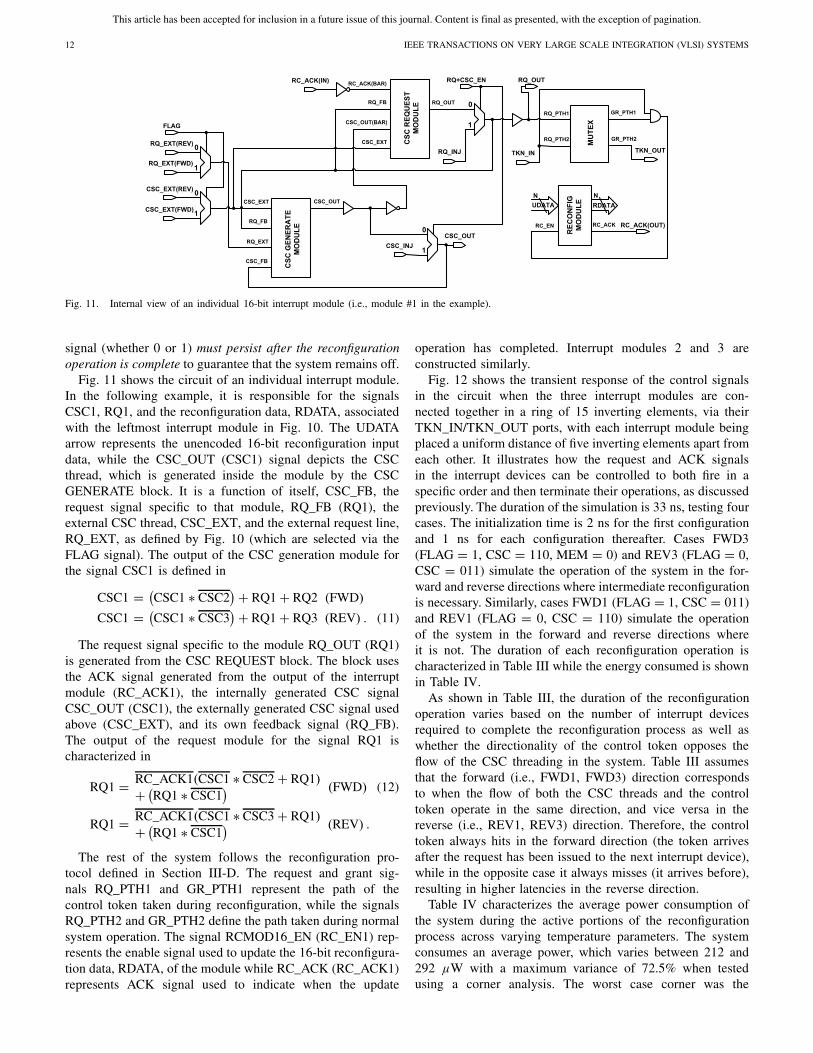
Fig. 11 shows the circuit of an individual interrupt module.In the following example, it is responsible for the signalsCSC1, RQ1, and the reconfiguration data, RDATA, associatedwith the leftmost interrupt module in Fig. 10. The UDATAarrow represents the unencoded 16-bit reconfiguration inputdata, while the CSC_OUT (CSC1) signal depicts the CSCthread, which is generated inside the module by the CSCGENERATE block. It is a function of itself, CSC_FB, therequest signal specific to that module, RQ_FB (RQ1), theexternal CSC thread, CSC_EXT, and the external request line,RQ_EXT, as defined by Fig. 10 (which are selected via theFLAG signal). The output of the CSC generation module forthe signal CSC1 is defined in
CSC1 = (CSC1 ∗ CSC2
)+ RQ1+ RQ2 (FWD)
CSC1 = (CSC1 ∗ CSC3
)+ RQ1+ RQ3 (REV) . (11)
The request signal specific to the module RQ_OUT (RQ1)is generated from the CSC REQUEST block. The block usesthe ACK signal generated from the output of the interruptmodule (RC_ACK1), the internally generated CSC signalCSC_OUT (CSC1), the externally generated CSC signal usedabove (CSC_EXT), and its own feedback signal (RQ_FB).The output of the request module for the signal RQ1 ischaracterized in
RQ1 = RC_ACK1(CSC1 ∗ CSC2 + RQ1)
+ (RQ1 ∗ CSC1
) (FWD) (12)
RQ1 = RC_ACK1(CSC1 ∗ CSC3 + RQ1)
+ (RQ1 ∗ CSC1
) (REV) .
The rest of the system follows the reconfiguration pro-tocol defined in Section III-D. The request and grant sig-nals RQ_PTH1 and GR_PTH1 represent the path of thecontrol token taken during reconfiguration, while the signalsRQ_PTH2 and GR_PTH2 define the path taken during normalsystem operation. The signal RCMOD16_EN (RC_EN1) rep-resents the enable signal used to update the 16-bit reconfigura-tion data, RDATA, of the module while RC_ACK (RC_ACK1)represents ACK signal used to indicate when the update
operation has completed. Interrupt modules 2 and 3 areconstructed similarly.
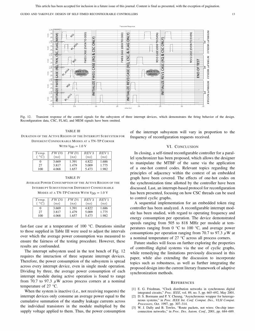
Fig. 12 shows the transient response of the control signalsin the circuit when the three interrupt modules are con-nected together in a ring of 15 inverting elements, via theirTKN_IN/TKN_OUT ports, with each interrupt module beingplaced a uniform distance of five inverting elements apart fromeach other. It illustrates how the request and ACK signalsin the interrupt devices can be controlled to both fire in aspecific order and then terminate their operations, as discussedpreviously. The duration of the simulation is 33 ns, testing fourcases. The initialization time is 2 ns for the first configurationand 1 ns for each configuration thereafter. Cases FWD3(FLAG = 1, CSC = 110, MEM = 0) and REV3 (FLAG = 0,CSC = 011) simulate the operation of the system in the for-ward and reverse directions where intermediate reconfigurationis necessary. Similarly, cases FWD1 (FLAG = 1, CSC = 011)and REV1 (FLAG = 0, CSC = 110) simulate the operationof the system in the forward and reverse directions whereit is not. The duration of each reconfiguration operation ischaracterized in Table III while the energy consumed is shownin Table IV.
As shown in Table III, the duration of the reconfigurationoperation varies based on the number of interrupt devicesrequired to complete the reconfiguration process as well aswhether the directionality of the control token opposes theflow of the CSC threading in the system. Table III assumesthat the forward (i.e., FWD1, FWD3) direction correspondsto when the flow of both the CSC threads and the controltoken operate in the same direction, and vice versa in thereverse (i.e., REV1, REV3) direction. Therefore, the controltoken always hits in the forward direction (the token arrivesafter the request has been issued to the next interrupt device),while in the opposite case it always misses (it arrives before),resulting in higher latencies in the reverse direction.
Table IV characterizes the average power consumption ofthe system during the active portions of the reconfigurationprocess across varying temperature parameters. The systemconsumes an average power, which varies between 212 and292 μW with a maximum variance of 72.5% when testedusing a corner analysis. The worst case corner was the
This article has been accepted for inclusion in a future issue of this journal. Content is final as presented, with the exception of pagination.
GUIDO AND YAKOVLEV: DESIGN OF SELF-TIMED RECONFIGURABLE CONTROLLERS 13
Fig. 12. Transient response of the control signals for the subsystem of three interrupt devices, which demonstrates the firing behavior of the design.Reconfiguration data, CSC, FLAG, and MEM signals have been omitted.
TABLE III
DURATION OF THE ACTIVE REGION OF THE INTERRUPT SUBSYSTEM FOR
DIFFERENT CONFIGURABLE MODES AT A TN-TP CORNER
WITH VDD = 1.0 V
TABLE IV
AVERAGE POWER CONSUMPTION OF THE ACTIVE REGION OF THE
INTERRUPT SUBSYSTEM FOR DIFFERENT CONFIGURABLE
MODES AT A TN-TP CORNER WITH VDD = 1.0 V
fast-fast case at a temperature of 100 °C. Durations similarto those supplied in Table III were used to adjust the intervalsover which the average power consumption was measured toensure the fairness of the testing procedure. However, theseresults are confounded.
The interrupt subsystem used in the test bench of Fig. 12requires the interaction of three separate interrupt devices.Therefore, the power consumption of the subsystem is spreadacross every interrupt device, even in single mode operation.Dividing by three, the average power consumption of eachinterrupt module during active operation is found to rangefrom 70.7 to 97.3 μW across process corners at a nominaltemperature of 27 °C.
When the system is inactive (i.e., not receiving requests) theinterrupt devices only consume an average power equal to thecumulative summation of the standby leakage currents acrossthe individual transistors in the module multiplied by thesupply voltage applied to them. Thus, the power consumption
of the interrupt subsystem will vary in proportion to thefrequency of reconfiguration requests received.
VI. CONCLUSION
In closing, a self-timed reconfigurable controller for a paral-lel synchronizer has been proposed, which allows the designerto manipulate the MTBF of the same via the applicationof a one-hot control codes. Relevant topics regarding theprinciples of adjacency within the context of an embeddedgraph have been covered. The effects of one-hot codes onthe synchronization time allotted by the controller have beendiscussed. Last, an interrupt-based protocol for reconfigurationhas been presented, focusing on how CSC threads can be usedto control cyclic graphs.
A sequential implementation for an embedded token ringcontroller has been analyzed. A reconfigurable interrupt mod-ule has been studied, with regard to operating frequency andenergy consumption per operation. The device demonstratedspeeds ranging from 505 to 818 MHz per module at tem-peratures ranging from 0 °C to 100 °C, and average powerconsumptions per operation ranging from 70.7 to 97.3 μW ata nominal temperature of 27 °C across all process corners.
Future studies will focus on further exploring the propertiesof controlling digital systems via the use of cyclic graphs,while remedying the limitations previously discussed in thispaper, while also extending the discussion to incorporatetopics such as robustness, as well as further integrating theproposed design into the current literary framework of adaptivesynchronization methods.
REFERENCES
[1] E. G. Friedman, “Clock distribution networks in synchronous digitalintegrated circuits,” Proc. IEEE, vol. 89, no. 5, pp. 665–692, May 2001.
[2] D. S. Bormann and P. Y. Cheung, “Asynchronous wrapper for heteroge-neous systems,” in Proc. IEEE Int. Conf. Comput. Des., VLSI Comput.Processors, Oct. 1997, pp. 307–314.
[3] W. J. Dally and B. Towles, “Route packets, not wires: On-chip inter-connection networks,” in Proc. Des. Autom. Conf., 2001, pp. 684–689.
This article has been accepted for inclusion in a future issue of this journal. Content is final as presented, with the exception of pagination.
14 IEEE TRANSACTIONS ON VERY LARGE SCALE INTEGRATION (VLSI) SYSTEMS
[4] E. Beigné, F. Clermidy, P. Vivet, A. Clouard, and M. Renaudin, “Anasynchronous noc architecture providing low latency service and itsmulti-level design framework,” in Proc. 11th IEEE Int. Symp. Asyn-chronous Circuits Syst., Mar. 2005, pp. 54–63.
[5] D. J. Kinniment, Synchronization & Arbitration in Digital Systems.New York, NY, USA: Wiley, 2007.
[6] T. Chelcea and S. M. Nowick, “Robust interfaces for mixed-timingsystems,” IEEE Trans. Very Large Scale Integr. (VLSI) Syst., vol. 12,no. 8, pp. 857–873, Aug. 2004.
[7] J. Jex and C. Dike, “A fast resolving binmos synchronizer for parallelprocessor interconnect,” IEEE J. Solid-State Circuits, vol. 30, no. 2,pp. 133–139, Feb. 1995.
[8] J. Zhou, D. Kinniment, G. Russell, and A. Yakovlev, “A robust syn-chronizer,” in Proc. IEEE Comput. Soc. Annu. Symp. Emerging VLSITechnol. Architectures, Mar. 2006, pp. 442–443.
[9] C. van Berkel, “Handshake circuits: An intermediary between com-municating processes and VLSI,” Ph.D. dissertation, Philips Res. Lab.Eindhoven, Technische Univ., Eindhoven, Netherlands, 1992.
[10] J. Ebergen, “Squaring the FIFO in GasP,” in Proc. 7th Int. Symp.Asynchronous Circuits Syst., Mar. 2001, pp. 194–205.
[11] C. Brej, “Wagging logic: Implicit parallelism extraction using asynchro-nous methodologies,” in Proc. 10th Int. Conf. Appl. Concurrency Syst.Des., 2010, pp. 35–44.
[12] M. Alshaikh, D. Kinniment, and A. Yakovlev, “A synchronizerdesign based on wagging,” in Proc. Int. Conf. Microelectron., 2010,pp. 415–418.
[13] J. U. Horstmann, H. W. Eichel, and R. L. Coates, “Metastability behaviorof CMOS ASIC flip-flops in theory and test,” IEEE J. Solid-StateCircuits, vol. 24, no. 1, pp. 146–157, Feb. 1989.
[14] J. Cortadella, Logic Synthesis for Asynchronous Controllers and Inter-faces, vol. 8. New York, NY, USA: Springer-Verlag, 2002.
[15] I. E. Sutherland and R. F. Sproull, “Logical effort: Designing for speedon the back of an envelope,” in Proc. University California/Santa CruzConf. Adv. Res. VLSI. 1991, pp. 1–16.
[16] U. Frank, T. Kapshitz, and R. Ginosar, “A predictive synchronizer forperiodic clock domains,” Formal Methods Syst. Des., vol. 28, no. 2,pp. 171–186, 2006.
[17] A. Martin, “Synthesis of asynchronous VLSI circuits,” Formal MethodsVLSI Des., vol. 2, pp. 237–283, Feb. 1990.
[18] T.-A. Chu, “Synthesis of self-timed VLSI circuits from graph-theoreticspecifications,” Ph.D. dissertation, Dept. Electr. Eng. Comput. Sci.,Massachusetts Inst. Technol., Cambridge, MA, USA, 1987.
[19] A. Kondratyev, J. Cortadella, M. Kishinevsky, E. Pastor, O. Roig,and A. Yakovlev, “Checking signal transition graph implementabilityby symbolic BDD traversal,” in Proc. Eur. Conf. Des. Test, 1995,pp. 325–332.
[20] J. Cortadella, M. Kishinevsky, A. Kondratyev, L. Lavagno, andA. Yakovlev, “Petrify: A tool for manipulating concurrent specificationsand synthesis of asynchronous controllers,” IEICE Trans. Inf. Syst.,vol. 80, no. 3, pp. 315–325, Mar. 1997.
[21] I. Poliakov, D. Sokolov, and A. Mokhov, “Workcraft: A static data flowstructure editing, visualisation and analysis tool,” in Proc. Petri NetsOther Models Concurrency, 2007, pp. 505–514.
[22] J. M. Rabaey, A. Chandrakasan, and B. Nikolic, Digital IntegratedCircuits: A Design Perspective. Upper Saddle River, NJ, USA: Prentice-Hall 2003.
[23] D. E. Muller and W. S. Bartky, “A theory of asynchronous circuits,” inProc. Int. Symp. Theory Switching, 1959, pp. 204–243.
[24] D. J. Kinniment, A. Bystrov, and A. V. Yakovlev, “Synchronizationcircuit performance,” IEEE J. Solid-State Circuits, vol. 37, no. 2,pp. 202–209, Feb. 2002.
[25] D. Sokolov, “Automated synthesis of asynchronous circuits using directmapping for control and data paths,” Ph.D. dissertation, Dept. SchoolElectr., Electron. Comput. Eng., Univ. Newcastle Upon Tyne, U.K.,2006.
James S. Guido (GSM’03) received the B.Sc.degree in electrical and computer engineering andthe M.Sc. degree in electrical engineering from theUnivesity of Rochester, Rochester, NY, USA, in2006 and 2008, respectively. He is currently pur-suing the Ph.D. degree in electrical, electronic, andcomputer engineering from Newcastle University,Newcastle upon Tyne, U.K.
He is a Post-Graduate Researcher with the Micro-electronics System Design Research Group, New-castle University. His current research interests
include the design of robust interfaces utilizing asynchronous circuits, withspecial interest on the reliable synchronization of such interfaces acrossdifferent interconnect technologies.
Alexandre Yakovlev (SM’97) received the M.Sc.and Ph.D. degrees from St. Petersburg ElectricalEngineering Institute, St. Petersburg, Russia, and theD.Sc. degree from Newcastle University, Newcastleupon Tyne, U.K., in 1979, 1982, and 2006, respec-tively.
He was involved in the area of asynchronous andconcurrent systems with St. Petersburg ElectricalEngineering Institute since 1980, and held positionsof an Assistant and Associate Professor with theComputing Science Department from 1982 to 1990.
Since 1991, he has been with Newcastle University, where he held aprofessorial position head with the Microelectronic Systems Design ResearchGroup, School of Electrical and Electronic Engineering. He has published fourmonographs and more than 300 papers in academic journals and conferences,and has managed over 25 research contracts. His current research interestsinclude in the field of modeling and design of asynchronous, concurrent, real-time, and dependable systems-on-a-chip.
Dr. Yakovlev is a member of IET and a Dream Fellow with Engineer-ing and Physical Sciences Research Council, Swindon, Wiltshire, U.K., toinvestigate different aspects of energy-modulated computing. He has chairedprogram committees of several international conferences, including the IEEEInternational Symposium on Asynchronous Circuits and Systems, Petri nets,and the Applications of Concurrency to Systems Design, and he has been theChairman of the Steering committee of the Conference on the Application ofConcurrency to System Design since 2001.