Embed Size (px)
Citation preview
Printing WearableDevices in 2D and 3D:An Overview onMechanical andElectronic DigitalCo-design
Samira Tansaz, Annalisa Baronetto,
Rui Zhang, Adrian Derungs, and Oliver Amft
Chair of Digital Health, Friedrich-Alexander
Universit€at Erlangen-N€urnberg
Abstract—Multiprocess Additive Manufacturing (AM) offers systemdesigners new, exciting
computational tools to rapidly realise smartwearable sensingdevices in two-dimensional
(2D) and3Dshapes.Weguide readers through thenovel development and fabrication
process basedonadigital co-design frameworkandhighlightAMtechniques, functional
materials, and assembly procedures for designing wearables as flexible and stretchable
on-skinpatches, e-textiles, andsmart accessories for everydayuse.
& WEARABLE DEVICE DESIGNERS are today chal-
lenged by multiple advanced user expectations
affecting function, practicality, aesthetics, and
fashion. Moreover, developers and researchers
of sports and wellness wearables are facing
short design cycles and may require product
personalization to achieve the system’s purpose.
Classic engineering and production processes
Digital Object Identifier 10.1109/MPRV.2019.2948819
Date of current version 21 January 2020.
Theme Article: Multiprocess Additive ManufacturingTheme Article: Multiprocess Additive Manufacturing
381536-1268 � 2019 IEEE Published by the IEEE Computer Society IEEE Pervasive Computing
are often too slow and cost-intensive to address
the wearable development needs, involving
steps to realize tools, masks, and molds for
mechanical parts as well as to manufacture and
assemble printed circuit boards. The versatility
and design freedom provided by modern addi-
tive manufacturing (AM) methods offer system
developers an alternative, highly appealing
approach to create wearable devices. In addition
to addressing the specific system requirements
of wearables, AM can provide developers of
wearable devices with design speed and update
flexibility similar to that enjoyed by mobile soft-
ware developers.
System requirements of wearable devices
are determined—among others—by the body
attachment, usability, and robustness: for exam-
ple, material choice determines haptic percep-
tion and function of printed sensors, form factor
determines handling in everyday situations,
mechanical flexibility, and stretchability deter-
mine body- and skin-conformal attachment.
Across various application fields, wearable
device categories with specific requirement sets
have evolved, including smart accessories (e.g.,
armbands, belts, eyeglasses), on-skin patches,
e-tattoos, and smart clothes1. Smart accessories
typically involve particular three-dimensional
(3D) mechanical designs, such as flexible bands
or rigid frames. Conversely, patches, e-tattoos,
and cloth-integrated devices often require stret-
chable 2D designs, which should not change the
physical appearance and thus should be as thin
as possible. Both, 2D and 3D wearable designs
are not only mechanically challenging to imple-
ment, but the mechanical design sets conditions
for electronics with sensor and interactive func-
tions. As a consequence, electronic circuits need
to be bendable and stretchable or get mounted
on nonplanar surfaces.
To leverage the possibilities of wearable tech-
nology for various application fields, system
developers need to co-designmechanics and elec-
tronics and incorporate the cross-effects of both
domains. Over the decades, the co-design has
been done by trial and error testing of prototypes.
With a combination of modern AM-based techni-
ques and software tools, digital co-design as well
as mechanical and electronic AM-fabrication is
becoming feasible in a multiprocess approach.
However, AM offers various process options that
substantially affect the outcome. While con-
stantly new components and improvements for
multiprocess AM are released, no methodologies
for integrated wearable device design have been
established yet. Presently, developers interested
in digital co-design and multiprocess AM are
forced to elaborate and experiment with the dif-
ferent process components first: the design and
manufacturing software components and interfa-
ces, as well as the AMhardware. Steps are needed
to bridge the gap.
This article introduces a framework for digi-
tal co-design using the multiprocess capabilities
of AM and maps it to 2D and 3D wearable
device design examples. Based on the co-design
framework, we offer guidance in process choice
across AM techniques, functional materials, and
assembly, for pervasive computing professionals
and wearable systems researchers. While the
basic AM processes are used in other domains
too, we emphasize the specific wearable device
requirements for shape, stretchability, comput-
ing, etc. We hope that the proposed frame-
work spurs research on digital co-design and
helps to broaden the design community that
makes wearables.
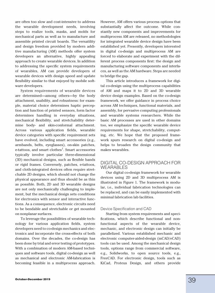
DIGITAL CO-DESIGN APPROACH FORWEARABLES
Our digital co-design framework for wearable
devices using 2D and 3D multiprocess AM is
illustrated in Figure 1. The framework is modu-
lar, i.e., individual fabrication technologies can
be replaced, and can be easily implemented with
minimal fabrication lab facilities.
Device Specification and CAD
Starting from system requirements and speci-
fications, which describe functional and non-
functional aspects of the wearable device,
mechanic, and electronic design can initially be
parallelized. Various established mechanic and
electronic computer-aided-design (mCAD/eCAD)
tools can be used. Among the mechanical design
tools, options range from commercial software,
e.g., Solidworks, to open source tools, e.g.,
FreeCAD. For electronic design, tools such as
KiCad, Proteus Design, and others provide
October-December 2019 39
developers with schematic and layout entry and
produce electronic design data that can be used
for the subsequent integration step.
mCAD and eCAD Integration
The draft mCAD and eCAD designs are then
integrated, depending on the targeted wearable
device shape: For 2D designs and substrates
that are planar during fabrication but shall con-
form to skin or objects later, integration involves
adjusting the electronic design to withstand
bending, stretching, or later 3D forming. For
example, a basic method to prevent conductive
lines from detaching or breaking is to add strain
relief, such as meander-shaped conductor lines
and varying line width. If the mechanical design
will be fabricated in 3D, additional integration
steps are needed. Here, the 3D shape integration
of eCAD and mCAD can be made by mapping and
optimizing the electronic layout on the planar
and nonplanar object surfaces. Some extended
mCAD tools support layout mapping, e.g., Solid-
works Electrical 3D and Catia. For 2D and 3D
shapes, the integration step may involve chang-
ing mechanical shapes, e.g., creating rigid, non-
bending regions in 2D designs, or adjusting line
routing to bypass steep ridges in 3D designs that
otherwise could lead to ruptures. During the
CAD integration, it is helpful to perform a design
check and adjust mechanics and electronics
depending on the choice of AM fabrication tech-
nology down the process chain. There are some
manufacturer tools that offer design checks,
however, the design of manufacturability is still
an open research field as it can be challenging to
project fabrication issues ahead of time.2
Material Selection
We include material selection subsequent to
the CAD design integration. However, it is likely
that assumptions about materials and their prop-
erties are beingmade earlier. Nevertheless, before
the actual fabrication, all material choices, includ-
ing compatibility analyses must be completed.
We provide an overview of functional material
choices to achieve specific properties (e.g.,
mechanical, optical, conductive) further below.
Mechanical AM and Postprocessing
The mechanical AM step aims to create a
base object and is commonly employed to either
create a 2D layer or a 3D shape, which serves as
a substrate for electronic circuits later. Alterna-
tively, for 2D designs, foils can be used as sub-
strates and to bypass the mechanical AM.
Various AM techniques exist, which provide
advanced material properties for wearable
designs, including stiffness, color, and elasticity.
AM techniques typically imply postprocessing
to achieve the desired performance, e.g., surface
smoothness.
Electronics AM
Based on the mechanical substrate, elec-
tronic circuits are added. For some electronic
components, an AM-based fabrication has been
demonstrated, including transistors, capacitors,
and batteries. Moreover, researchers have used
AM techniques successfully to fabricate sensors,
e.g., strain-sensitive elements. However, the
functionality, performance, and size of various,
commonly used passive elements, such as resis-
tors, capacitors, as well as active ones, like
Figure 1. Digital co-design framework for 2D and 3D wearable devices using multiprocess AM.
Multiprocess Additive Manufacturing
40 IEEE Pervasive Computing
microcontrollers, cannot be efficiently repli-
cated using AM. Hence, electronic component
placement is an important step toward a func-
tional wearable device and can be arranged—
depending on design needs—before or after any
AM-based component and sensor fabrication.
Classical electronics production uses a
fixed scheme of producing circuit boards with
alternating layers of conductors and insulation
followed by soldering components onto the
board, i.e., by reflow soldering. Since AM-based
circuit fabrication typically uses temperature-
sensitive plastic substrates, it must avoid
temperatures above approx. 150 �C. As a con-
sequence, several alternative printed electron-
ics processes are being developed that vary
the order and method of electronic compo-
nents, sensors, and conductor fabrication.
When components are placed or fabricated
before adding conductive lines, a robust inter-
connection technique is to print on the
mechanical design using conductive materials
from pad to pad of the placed components,
e.g., inks with silver particles.
Similar to the mechanical AM, electronics AM
requires postprocessing, e.g., curing conductive
inks with UV light or heat drying. Key techniques
for electronic AM, postprocessing, and assembly
options for 2D and 3D designs are discussed fur-
ther below.
Fabrication Iterations
For some wearable designs, further iterations
of mechanical and electronics AM may be neces-
sary, e.g., to enclose circuits, or add further func-
tional elements using alternative AM techniques.
A key challenge for design iterations, where
existing mechanical shapes are extended, is the
accurate device alignment in the subsequent AM
machine’s print chamber. Many AM manufac-
turers currently do not support design iterations
or require manual tool path specifications,
which can be time-consuming and error-prone
efforts for complex designs. However, once all
postprocessing is completed, the device is
immediately ready for use.
AM TECHNIQUESAM is the most recent name given to the vari-
ous fabrication techniques to produce high-
value parts with complex geometries, also
termed 3D printing, rapid manufacturing, solid
freeform fabrication, or rapid prototyping.3,4
The different AM terms imply process technolo-
gies that apply the consecutive delivery of
energy or material to create 2D and 3D struc-
tures directly,5 without the use of a prefabri-
cated mold.4 Objects are fabricated in a layer-by-
layer process based on CAD data. AM techniques
achieve a high degree of reproducibility, auto-
mation, design freedom, and personalization.6
For each AM fabrication technique, various
printing systems have been developed.
Mechanical AM
For mechanical AM of substrates and enclo-
sures, a variety of established 3D printing techni-
ques might be utilized, including fused
deposition modeling (FDM), laminated object
manufacturing, stereolithography apparatus
(SLA), and digital light processing (DLP), photo-
polymer jetting, multi jet fusion (MJF)/high
speed sintering (HSS), selective laser sintering
(SLS), and selective laser melting. Table 1 lists
selected AM techniques. Some of the techniques
need postprocessing like washing or cutting to
finish a part. Furthermore, UV or heat curing dur-
ing and after fabrication are frequently used.
Each technique has advantages and disadvan-
tages. For instance, FDM uses heat-based lique-
faction to extrude material. The FDM material
choice is centered to create solid mechanical
structures with infill whereas jetting techniques
use liquid photopolymer inks that can be func-
tionalized with additives. Moreover, the FDM
process is slower and produces a visual lining
due to the bead deposition requiring post-proc-
essing. However, FDM is a robust AM technique,
costs less than photopolymer jetting, and can
deliver mechanically reliable rigid substrates for
wearable accessories. SLA and binder jetting var-
iants are direct alternatives to FDM, however,
presently with fewer material options. Photo-
polymer jetting techniques, such as inkjet print-
ing, offer complementary material properties to
FDM. Photopolymer jetting is suitable for benda-
ble and stretchable mechanical and electronic
structures, thus fit for skin patches, print-on-tex-
tile, or strain-sensitive sensors. Inkjet printing
can produce solid 3D structure too, however,
October-December 2019 41
prints often deteriorate quickly, as discussed
along with material options below. SLS, MJF, and
HSS produce free-form 3D geometry, as they do
not need an additional support structure. How-
ever, MJF and HSS currently offer limited mate-
rial choices, and industry quality SLS systems
are still high in cost.
Electronics AM
Printing sensing components, conductive
traces, and circuits can be achieved with differ-
ent printing techniques too, including screen,
inkjet, and aerosol jet printing (see Table 1).
Both inkjet and aerosol jet printing are based
on the direct ink writing approach, i.e., a non-
contact deposition of inks onto flexible and
rigid substrates through nozzles. Structures are
fabricated by either moving nozzles or sub-
strate to achieve preferable properties, such as
minimizing material waste.7 However, when
printing should be done on 3D surfaces or
devices, such as adding conductive lines, print-
heads and substrates need to move together. A
5-axes motion is needed to reach all 3D surface
locations, which is dominated by noncontact
photopolymer jetting methods. All three
printed electronics techniques require postpro-
cessing, including sintering, heating, laser or
UV curing, and drying steps, depending on the
substrates and inks used. Print resolution, i.e.,
minimum trace width, is finest for aerosol jet-
ting (down to 10 mm), which is useful, e.g., to
create low pitch signal lines. However, ink jet-
ting and screen printing offer a wide range of
up to 100 mm, which reduces wait time when
printing regions, e.g., conductive electrodes.
Inkjet printing has comparably tight require-
ments on ink viscosity, which limits material
choices. Both jetting techniques outperform
screen printing on minimal layer thickness
(down to 0.1 mm), which helps to make high-
resolution structures.
Table 1. Comparison of key AM techniques for wearable fabrication. Based on Chu et al.,8 Gibson et al.,9 and manufacturer data as
listed in the cells.
Technique
XY Print
Resolution
(mm)
Ink
viscosity
(cP)
Thickness
of the
printed
layer (mm)
Material
application
Primary
use for
2D/3D
devices
Advantages Limitations
Screen printing 30–100 500–5000 5–100 Contact 2DVersatility for
inksFrame based
Aerosol printing 10 1–2500 0.1–5 Non-contact 3DVersatility for
inksHigh cost
Inkjet printing 15–100 10–30 0.5–3 Non-contact2D and
3DLow cost
For highly viscous
inks and high
aspect ratio
particle inks
Fused deposition
modeling (FDM)
10–300
(Tractus3D)–
50–300
(Tractus3D)
Non-contact,
extruding
heated beat
3D
Low cost,
material
choice for
solid
structures
Low print speed,
must liquify
material with heat
Multi jet fusion
(MJF), high speed
sintering (HSS)
40–60 (HP,
Voxeljet)–
70–150 (HP,
Voxeljet)
Contact
(powder
and binder
deposition)
3D
No add.
support
structure
Limited material
choice
Stereolithography
apparatus (SLA)
100–200
(Formlabs)–
25–200
(Formlabs)Non-contact 3D
Smooth
surfaces, no
add. support
structure
Limited material
choice
Selective laser
sintering (SLS)
125–200
(EOS)–
50–100
(EOS)
Contact
(powder
deposition)
3D
Almost any
material, no
add. support
structure
Rough surface,
limited powder
recycling
Multiprocess Additive Manufacturing
42 IEEE Pervasive Computing
Evaluation
Testing against the wearable device specs
should include bending, stretching tests, and
cleaning tests to assess reliability. In addition,
the functional test in varying environmental con-
ditions should be included.
FUNCTIONAL MATERIALSThe success of AM can be attributed to inno-
vations in material science and engineering
resulting in novel inks, substrates, and postpro-
cessing methods for various applications. Differ-
ent material types, including metals, ceramics,
polymers, and composites, can be exploited.
Material composition can be optimized to
achieve specific properties for wearable devices,
including transparent, flexible, stretchable, or
conductive function. Nevertheless, biocompati-
bility is a critical challenge for some materials
that are temporary or permanently in contact
with the skin.
Corresponding to the on-body application,
researchers have made efforts to develop wear-
ables that can fold, bend, stretch, which involves
excessive tensile stress. To convert rigid circuit
boards into flexible and stretchable designs,
organicmaterials including polymers are essential.
The flexibility and to some extent stretchability
of the device can be provided by using thermo-
plastic polymers and elastomers, respectively.
Nevertheless, the fabrication of devices that are
able to respond to large strain deformation with-
out fracture or significant performance degrada-
tion is still challenging.
Both, sensing and conductive elements are
fabricated by printing the circuit layout using
conductive inks on 2D substrates or 3D shapes.
Typical conductive materials include conductive
metal particles or flakes, including silver, cop-
per, carbon-based conductive fiber, tubes, or
polymer conductive inks, including PEDOT:PSS.
Table 2 provides an overview of conductive and
nonconductive ink materials, filaments, and sub-
strates. The conductive ink, in particular for liq-
uid metal and carbon inks, requires organic
binders to hold the material composition
together and ensure homogeneous dispersion.
The organic binders can also add flexibility and
stretchability to the inks. The optimal choice of
binder is related to the printed device design.
For example, thermoplastic polyurethane (TPU)
as a binder can provide flexibility and stretch-
ability. Some polymeric binders need to be
cured by heat or UV treatment. For instance,
acrylic urethane and silicone binders have been
developed for flexible and stretchable inks.
Another essential part of any ink is a solvent,
which gives flow to the ink. The solvent can pro-
vide an appropriate solubility to the organic
binder molecules, as well as provide the desired
homogeneity and viscosity.10 Alcohols, esters,
and ketones are popular solvents. Several non-
conductive materials could be used to create
insulator layers, 2D substrates, or 3D shapes.
The different surface morphology will provide
rough or smooth haptic feedback and determine
how further materials, e.g., conductive ink, adhe-
sive glue, can attach. For example, while gener-
ally, a rough morphology offers better
adhesiveness, it could also soak up and disperse
ink, resulting in blurred, imprecise structures.
Postprocessing, such as sanding or grinding can
convert rough surfaces into smooth ones.
ASSEMBLYResearchers actively investigate how to inte-
grate AM-fabricated components, conductive cir-
cuit lines, and off-the-shelf components on
mechanical substrates. The choice of assembly
approach depends on the wearable design,
selected materials, and AM techniques. By taking
the order of component and conductor place-
ment as guidance, the main two process arms
are: (A) first create the AM-fabricated compo-
nents and circuit layout on the substrate, poten-
tially with several conductive and insulating
layers, then place components, or (B) first fabri-
cate and/or place components on the substrate,
then print conductive ink on substrate and com-
ponent pads.
Print Circuit Then Add Components
The procedure follows the traditional-printed
circuit board manufacturing process and sup-
ports multilayer circuits with all typical features,
e.g., VIAs. Using heat-sensitive substrates, e.g.,
printed plastic structure or polymer foils implies
that components must be attached without
heat-based soldering. The primary alternative to
soldering is to accurately deposit conductive
October-December 2019 43
glue between the component pad and conduc-
tive trace.11 The glue potentially increases termi-
nal resistance due to the additional material
layer.
Add Components Then Interconnect
A convenient alternative to the classic assem-
bly order is to print on the component pads with
a conductive ink. The approach can be applied
to 2D and 3D designs, but limits developers to
single-layer circuits and components with
exposed pads. For example, microcontrollers in
chip-scale or ball packages often require multi-
layer circuits and connecting pads underneath
the package, which cannot be achieved here.
Electronic components can be placed, either
manually or using pick and place machines. As
AM machines and pick and place machines have
similar motion capabilities, component place-
ment can be done within AM machines. For
example, a printing nozzle can pick components
using a vacuum, as well as move and deposit
them to the target position.
DESIGNING WEARABLES IN 2DPrinting planar electronic designs on soft,
flexible, and stretchable substrates are widely
investigated for skin-conformal wearable health
and sports devices. Depending on the body
region, patch size, and sensor function, different
substrates and inks can be utilized. To illustrate
the co-design framework, we describe here two
studies that utilize AM and highlight key process
steps.
Valentine et al.12 developed a textile-attached
strain sensor garment to monitor joint bending
[Figure 2(b) and (c)] and an insole sensor array
to monitor human foot pressure [Figure 2(d)].
After determining a wearable specification, con-
sidering measurement function, body position,
and outfit integration (see Figure 1), they created
Table 2. Examples of conductive and nonconductive ink materials, filaments and substrates and their key properties for printing
wearable systems.
Material Properties
Additional sensing
and conductive
function
Form
Typical
AM
technique
Surface
morphology
Polylactic acid (PLA)Nonconductive/
rigid polymer– Filament FDM Rough
Acrylonitrile butadiene
styrene (ABS)
Resistance and
tough polymer– Filament FDM Rough
Polyurethane (PU),
Thermoplastic polyurethane
(TPU)
Flexible/
stretchable
polymer
Multiwall carbon
nanotubes, nano
silver particles
Filament/ink/
substrate (without
active components)
FDM,
inkjet
Rough,
smooth
Polycaprolactone (PCL)Biodegradable
polymer– Substrate FDM Rough
Polypyrrole (PPy)Biodegradable
polymer
Self-conductive
polymerInk Inkjet Smooth
Silicon rubberFlexible
polymer– Substrate Inkjet Smooth
Polyvinylidene (di-)fluoride
(PVDF)
Piezoelectric
polymer
Self-piezoelectric
polymerInk, Filament
Inkjet,
FDM
Smooth,
rough
Polyethylene terephthalate
(PET)
Flexible
polymer– Substrate FDM Rough
Nano copper, gold and nano
silver
Conductive
metal
Self-conductive
metalInk Inkjet Smooth
Poly(3,4-
ethylenedioxythiophene)
polystyrene sulfonate (PEDOT:
PSS)
Conductive
polymer
Self-conductive
polymerInk Inkjet Smooth
Multiprocess Additive Manufacturing
44 IEEE Pervasive Computing
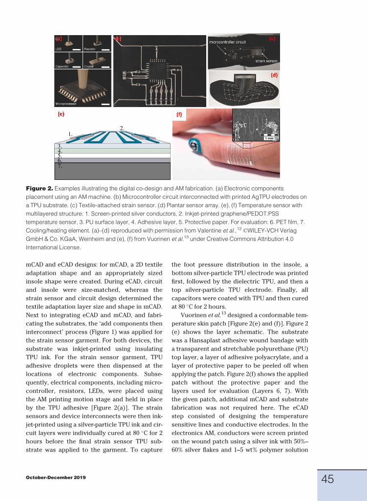
mCAD and eCAD designs: for mCAD, a 2D textile
adaptation shape and an appropriately sized
insole shape were created. During eCAD, circuit
and insole were size-matched, whereas the
strain sensor and circuit design determined the
textile adaptation layer size and shape in mCAD.
Next to integrating eCAD and mCAD, and fabri-
cating the substrates, the ‘add components then
interconnect’ process (Figure 1) was applied for
the strain sensor garment. For both devices, the
substrate was inkjet-printed using insulating
TPU ink. For the strain sensor garment, TPU
adhesive droplets were then dispensed at the
locations of electronic components. Subse-
quently, electrical components, including micro-
controller, resistors, LEDs, were placed using
the AM printing motion stage and held in place
by the TPU adhesive [Figure 2(a)]. The strain
sensors and device interconnects were then ink-
jet-printed using a silver-particle TPU ink and cir-
cuit layers were individually cured at 80 �C for 2
hours before the final strain sensor TPU sub-
strate was applied to the garment. To capture
the foot pressure distribution in the insole, a
bottom silver-particle TPU electrode was printed
first, followed by the dielectric TPU, and then a
top silver-particle TPU electrode. Finally, all
capacitors were coated with TPU and then cured
at 80 �C for 2 hours.
Vuorinen et al.13 designed a conformable tem-
perature skin patch [Figure 2(e) and (f)]. Figure 2
(e) shows the layer schematic. The substrate
was a Hansaplast adhesive wound bandage with
a transparent and stretchable polyurethane (PU)
top layer, a layer of adhesive polyacrylate, and a
layer of protective paper to be peeled off when
applying the patch. Figure 2(f) shows the applied
patch without the protective paper and the
layers used for evaluation (Layers 6, 7). With
the given patch, additional mCAD and substrate
fabrication was not required here. The eCAD
step consisted of designing the temperature
sensitive lines and conductive electrodes. In the
electronics AM, conductors were screen printed
on the wound patch using a silver ink with 50%–
60% silver flakes and 1–5 wt% polymer solution
Figure 2. Examples illustrating the digital co-design and AM fabrication. (a) Electronic components
placement using an AM machine. (b) Microcontroller circuit interconnected with printed AgTPU electrodes on
a TPU substrate. (c) Textile-attached strain sensor. (d) Plantar sensor array. (e), (f) Temperature sensor with
multilayered structure: 1. Screen-printed silver conductors, 2. Inkjet-printed graphene/PEDOT:PSS
temperature sensor, 3. PU surface layer, 4. Adhesive layer, 5. Protective paper. For evaluation: 6. PET film, 7.
Cooling/heating element. (a)–(d) reproduced with permission from Valentine et al.,12 �WILEY-VCH Verlag
GmbH & Co. KGaA, Weinheim and (e), (f) from Vuorinen et al.13 under Creative Commons Attribution 4.0
International License.
October-December 2019 45
diluted in a solvent. After curing the printed sil-
ver conductors in a convection oven at 130 �Cfor 13 min, and since no integrated electronic
components were needed, the electronics AM
process was repeated for the temperature sen-
sor. The temperature sensor was then inkjet-
printed using a graphene/PEDOT:PSS ink and
cured at 130 �C for 10 minutes. The analysis con-
firmed that the patch can detect temperatures
between 35 and 45 �C. From the digital co-design
approach, the lack of integrated electronics sim-
plified the approach.
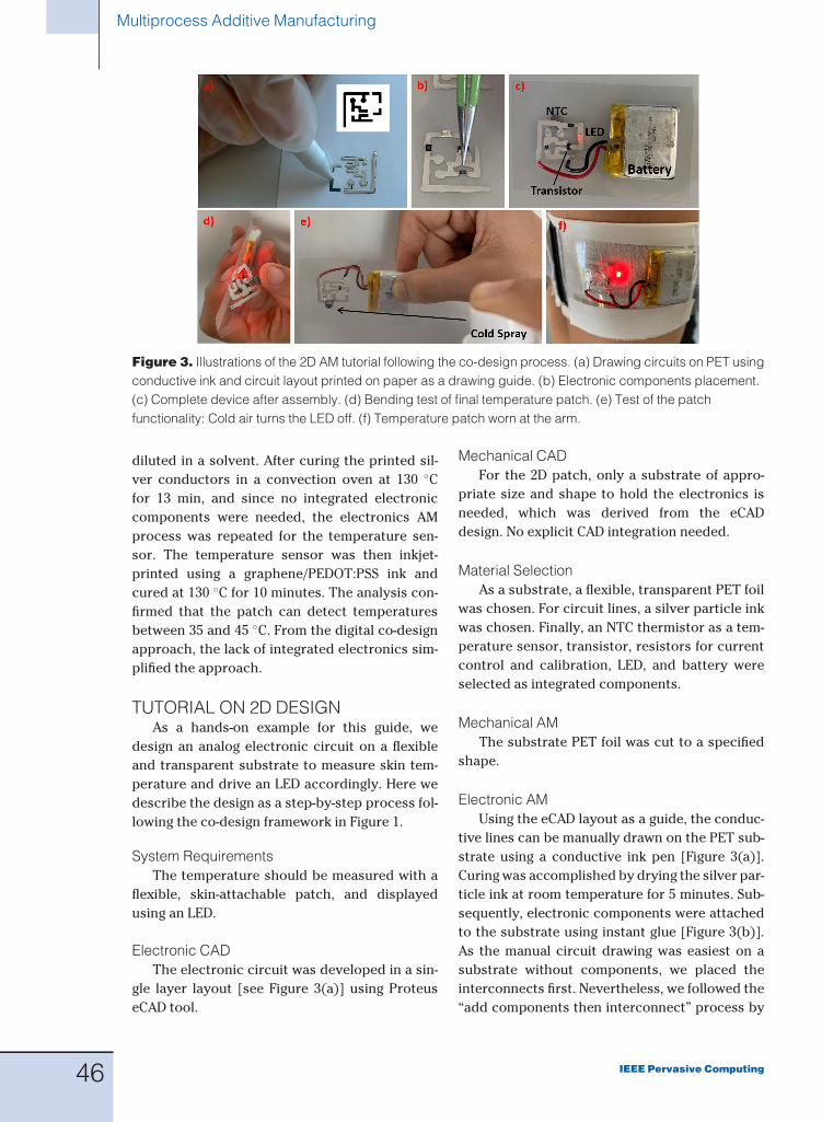
TUTORIAL ON 2D DESIGNAs a hands-on example for this guide, we
design an analog electronic circuit on a flexible
and transparent substrate to measure skin tem-
perature and drive an LED accordingly. Here we
describe the design as a step-by-step process fol-
lowing the co-design framework in Figure 1.
System Requirements
The temperature should be measured with a
flexible, skin-attachable patch, and displayed
using an LED.
Electronic CAD
The electronic circuit was developed in a sin-
gle layer layout [see Figure 3(a)] using Proteus
eCAD tool.
Mechanical CAD
For the 2D patch, only a substrate of appro-
priate size and shape to hold the electronics is
needed, which was derived from the eCAD
design. No explicit CAD integration needed.
Material Selection
As a substrate, a flexible, transparent PET foil
was chosen. For circuit lines, a silver particle ink
was chosen. Finally, an NTC thermistor as a tem-
perature sensor, transistor, resistors for current
control and calibration, LED, and battery were
selected as integrated components.
Mechanical AM
The substrate PET foil was cut to a specified
shape.
Electronic AM
Using the eCAD layout as a guide, the conduc-
tive lines can be manually drawn on the PET sub-
strate using a conductive ink pen [Figure 3(a)].
Curingwas accomplished by drying the silver par-
ticle ink at room temperature for 5 minutes. Sub-
sequently, electronic components were attached
to the substrate using instant glue [Figure 3(b)].
As the manual circuit drawing was easiest on a
substrate without components, we placed the
interconnects first. Nevertheless, we followed the
“add components then interconnect” process by
Figure 3. Illustrations of the 2D AM tutorial following the co-design process. (a) Drawing circuits on PET using
conductive ink and circuit layout printed on paper as a drawing guide. (b) Electronic components placement.
(c) Complete device after assembly. (d) Bending test of final temperature patch. (e) Test of the patch
functionality: Cold air turns the LED off. (f) Temperature patch worn at the arm.
Multiprocess Additive Manufacturing
46 IEEE Pervasive Computing
adding silver particle ink droplets on the compo-
nent pins to create the connection between pins
and conductive lines. The temperature sensor
was connected through two holes filled with the
ink and placed on the opposite side of the circuit.
In the same way, the wires of the external battery
were attached to the drawn lines. Figure 3(c)
shows the final device after assembly.
Evaluation
Figure 3(d) illustrates a manual bending test
to assess reliability, which can be automated
with a bending test machine. In Figure 3(e), the
functional test by varying environmental temper-
ature is shown.
In this 2D design approach, we replicated the
process steps that would be performed by elec-
tronics AM manually. While the quality of
manual AM is not lower than that of an auto-
mated fabrication process and many implemen-
tation details can be optimized, our tutorial
illustrates the co-design approach. Our proto-
type could be integrated into a wearable device,
e.g., an armband, for initial on-body functional
tests, as Figure 3(f) shows. Here, the circuit was
taped to an armband. Alternatively, the circuit
could be attached directly to a textile, using an
intermediate layer between the circuit and the
substrate to avoid an ink absorption in the fab-
ric. As Rivera et al.14 describe, some measures
need to be taken to avoid unwanted textile
movements when printing with a nozzle. A com-
plementary manual approach for making 2D
wearables was presented by Nagels et al.15
DESIGNING WEARABLES IN 3DWhile the mechanical AM for 3D designs is
widely established, AM-based circuit fabrication
in 3D is an open topic. One approach to 3D-
shaped electronics is to initially deposit conduc-
tors and electronic components onto a planar
substrate, i.e., using 2D methods, and subse-
quently, employ thermoforming to obtain a 3D
part. However, due to the deformation and
thermal stresses, the method is only suitable
for certain substrates, inks, and optimized cir-
cuit designs.
Another 3D electronics printing approach is to
attach components on any nonplanar surfaces
and realize circuit contacts as described in the co-
design framework above, either by creating the
circuit before or print on component pads after
the placement. An AM machine with five movable
axes can reach all surfaces of the 3D substrate.
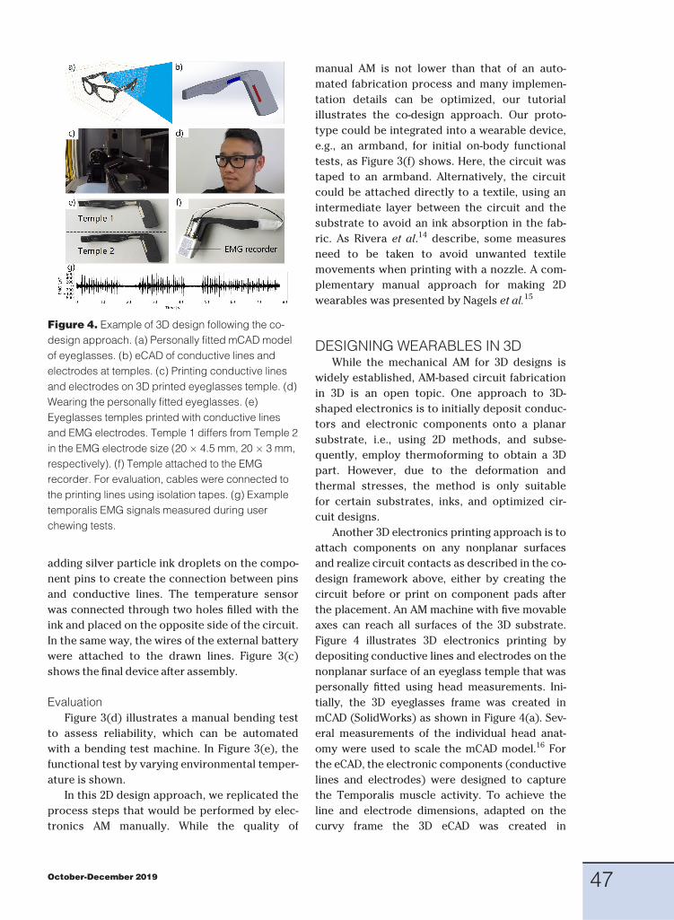
Figure 4 illustrates 3D electronics printing by
depositing conductive lines and electrodes on the
nonplanar surface of an eyeglass temple that was
personally fitted using head measurements. Ini-
tially, the 3D eyeglasses frame was created in
mCAD (SolidWorks) as shown in Figure 4(a). Sev-
eral measurements of the individual head anat-
omy were used to scale the mCAD model.16 For
the eCAD, the electronic components (conductive
lines and electrodes) were designed to capture
the Temporalis muscle activity. To achieve the
line and electrode dimensions, adapted on the
curvy frame the 3D eCAD was created in
Figure 4. Example of 3D design following the co-
design approach. (a) Personally fitted mCAD model
of eyeglasses. (b) eCAD of conductive lines and
electrodes at temples. (c) Printing conductive lines
and electrodes on 3D printed eyeglasses temple. (d)
Wearing the personally fitted eyeglasses. (e)
Eyeglasses temples printed with conductive lines
and EMG electrodes. Temple 1 differs from Temple 2
in the EMG electrode size (20 � 4.5 mm, 20 � 3 mm,
respectively). (f) Temple attached to the EMG
recorder. For evaluation, cables were connected to
the printing lines using isolation tapes. (g) Example
temporalis EMG signals measured during user
chewing tests.
October-December 2019 47
SolidWorks taking the mCAD model as a basis
[Figure 4(b)]. For mechanical AM, we used HP
nylon plastic PA2200 and an HP MJF 3D printer to
fabricate the temple according to the mCAD
design. For the subsequent electronics AM, piezo
inkjetting was used to deposit conductive ink
using a 5-axes AMmachine (CNCMotion Platform,
NeoTech Amt, Germany), as shown in Figure 4(c).
Lines and electrodes were printed in a single layer
and dried at room temperature. Figure 4(d) shows
the fabricated eyeglasses worn. Figure 4(e) shows
the 3D-printed eyeglasses temples with the depos-
ited conductive components. Zhang et al.17 evalu-
ated conductivity and found line resistance of 4.31
� 0.97V across 8.5 cm line length, at 5 mA current
applied. Electrodes of 20 � 4.5 mm were analyzed
using 4-terminal impedance measurements yield-
ing 0.10 � 0.02 V. In a user test to measure the
Electromyogram (EMG) of the Temporalis muscle
using the setup in Figure 4(f), we observed an
acceptable EMG signal to noise ratio and muscle
contraction during chewing could be detected. An
example recording from the fabricated eyeglasses
temple is shown in Figure 4(g).
Obtaining reliable conductors using 3D print-
ing can be particularly challenging at surface
edges. We observed that conductors are particu-
larly likely to break at orientation changes with
angles of 90� ormore. Printingmultiple ink layers,
altering printing speed at bends, or using alterna-
tive curing methods likely reduces the chance of
breaks. Using co-design iterations and additional
sealing steps could improve the robustness and
insulation of the conductive layers.
FUTURE OF AM FOR WEARABLESMultiprocess AM has made substantial prog-
ress over the last few years, enabling system
designers to create functional wearable devices.
Various materials have been developed to fabri-
cate conductors, sensors, or realize other prop-
erties. For example, strain or pressure-sensitive
inks can be applied for deformation sensors,
humidity-sensitive inks as moisture sensors, and
piezoelectric inks for energy harvesting and
touch sensors. A full review of the current wear-
able AM literature is beyond the scope of this
article. We selected literature to illustrate key
process steps. With the digital co-design
approach presented, we aim to help wearable
researchers and developers in understanding
and combining the strengths of different AM
techniques to realize a fully digital process chain
from a wearable model to the physical 2D or 3D
wearable device.
To leverage the complementary features of
different AM technologies MacDonald and
Wicker18 proposed to automate object handling
between machines. Ideally though, any wearable
device could be completely fabricated using a
single multiprocess AMmachine. Given the diver-
sity of mechanical functions and electronic fea-
tures needed for wearables, a single machine is
unlikely becoming feasible anytime soon. Still,
there are further challenges ahead for AM: For
one, replicating multilayer printed circuit boards
with the same miniature feature sizes and electri-
cal performance as in traditional processes is an
open problem. Here is where librarieswith select-
able digital design patterns can become helpful.
Another challenge is that printing on component
pads cannot be used with all electronic compo-
nent packages. Ultimately though, a key issue is
that classic reflow soldering is not an option for
the materials and substrates considered in AM.
Current AM process research targets methods to
replicate the reflowwithout heating. Althoughwe
have not addressed direct skin printing of wear-
able designs as electronic tattoos19 similar chal-
lenges can be expected as the patches, textiles,
and accessories described here.
A key challenge forwearable devices is durabil-
ity under environmental stresses, including sweat-
ing, temperature fluctuations, mechanical forces
such as bending or stretching, and cleaning. AM
already offers several measures tomaximize dura-
bility, however, their effect and interaction need
iterations of co-design and evaluation:
� mCAD & mechanical AM: Encapsulation and
sealing of the conductive traces with some
elastic and biocompatible polymers, to mini-
mize wear. Test using exposure to body,
washing cycles.
� Electronics AM: Printing conductors with
multiple layers to maximize conductivity.
Test: Line resistance and impedance analysis.
� eCAD & materials: Using trace layouts, e.g.,
S-shape, and stretchable substrate and
Multiprocess Additive Manufacturing
48 IEEE Pervasive Computing

stretchable inks to optimize skin-conformity.
Test: Bending or stretching machine tests to
measure force and changes in line or connec-
tor resistance.
It is conceivable that wearable systems may
be fabricated in fully automated AM production
hubs in the future. To leverage the digital co-
design and production hubs more comfortable
mCAD/eCAD tools, process abstraction, and digi-
tal design patterns, e.g., for an antenna, a strain
sensor, etc., are needed. A key consideration for
the massive use of AM to create wearables will be
sustainability. Thus, AM fabrication methods of
wearable devices must incorporate component
recycling and biodegradable materials. Degrad-
able metals including iron (Fe), Magnesium (Mg),
Zinc (Zn), and degradable polymers like PEDOT
can be utilized as a conductor. For substrates,
PLA, cellulose, and starch-based biodegradable
polymers can be an option.
ACKNOWLEDGMENTSThe authors would like to thank Mirco
S€uttenbach andMartin Hedges from Neotech AMT
for their helpwith the 3D electronics AMandVladi-
mir Kolbin from the FAU Chair of Digital Health for
helping with the temperature patch circuit design.
The authors also thank the reviewers for helping
to refine the manuscript. This work has been par-
tially funded by the EU H2020 MSCA ITN ACROSS-
ING project (GA no. 616757).
& REFERENCES
1. O. Amft and K. Van Laerhoven, “What will we wear
after smartphones?,” IEEE Pervasive Comput., vol. 16,
no. 4, pp. 80–85, Oct.–Dec. 2017.
2. I. Gibson, D. Rosen, and B. Stucker, “Design
for additive manufacturing,” in Additive
Manufacturing Technologies. New York, NY, USA:
Springer, pp. 399–435, 2015.
3. D. Hotza, C. M. Gomes, and J. G€unster, “Advances in
additive manufacturing processes and materials,”
Adv. Mech. Eng., vol. 6, 2014, Art. no. 645075. doi:
10.1155/2014/645075.
4. D. W. Hutmacher, M. Sittinger, and M. V. Risbud,
“Scaffold-based tissue engineering: rationale for
computer-aideddesign and solid free-form fabrication
systems” Trends Biotechnol., vol. 22, pp. 354–62, 2004.
5. T. Billiet, M. Vandenhaute, J. Schelfhout, S. Van
Vlierberghe, and P. Dubruel, “A review of trends and
limitations in hydrogel-rapid prototyping for tissue
engineering biomaterials,” vol. 33, pp. 6020–6041, 2012.
6. T. J€ungst, W. Smolan, K. Schacht, T. Scheibel, and
J. Groll, “Strategies and molecular design criteria
for 3D printable hydrogels,” Chem. Rev., vol. 116,
pp. 1496–539, 2016.
7. S. Khan, L. Lorenzelli, and R. S. Dahiya, “Technologies
for printing sensors and electronics over large flexible
substrates: A review,” IEEE Sens. J., vol. 15, no. 6,
pp. 3164–3185, Jun. 2015.
8. Y. Chu, C. Qian, P. Chahal, and C. Cao, “Printed
diodes: Materials processing, fabrication, and
applications,” Advanced Science - Wiley Online
Library, 2019. [Online]. Available: https://onlinelibrary.
wiley.com/doi/full/10.1002/advs.201801653
9. I. Gibson, D. Rosen, and B. Stucker, Additive
Manufacturing Technologies: 3D Printing, Rapid
Prototyping, and Direct Digital Manufacturing. New
York, NY, USA: Springer, 2015.
10. J. Kim, R. Kumar, A. J. Bandodkar, and J. Wang,
“Advanced materials for printed wearable
electrochemical devices: A review,” Adv. Electron.
Mater., vol. 3, no. 1, 2017, Art. no. 1600260.
11. J. van den Brand et al., “Flexible and stretchable
electronics for wearable health devices,” Solid-State
Electron., vol. 113, pp. 116–120, Nov. 2015.
12. A. D. Valentine et al., “Hybrid 3D printing of soft
electronics,” Adv. Mater., vol. 29, no. 40, Oct. 2017,
Art. no. 1703817.
13. T. Vuorinen, J. Niittynen, T. Kankkunen, T. M. Kraft,
and M. M€antysalo, “Inkjet-printed graphene/PEDOT:
PSS temperature sensors on a skin-conformable
polyurethane substrate,” Sci. Rep., vol. 6, Oct. 2016,
Art. no. 35289.
14. M. L. Rivera, M. Moukperian, D. Ashbrook,
J. Mankoff, and S. E. Hudson, “Stretching the
bounds of 3D printing with embedded textiles,” in
Proc. CHI Conf. Hum. Factors Comput. Syst., 2017,
pp. 497–508.
15. S. Nagels, R. Ramakers, K. Luyten, and W. Deferme,
“Silicone devices: A scalable DIY approach for
fabricating self-contained multi-layered soft circuits
using microfluidics,” in Proc. CHI Conf. Hum. Factors
Comput. Syst., 2018, pp. 188:1–188:13.
16. F. Wahl, R. Zhang, M. Freund, and O. Amft,
“Personalizing 3D-printed smart eyeglasses to
augment daily life,” IEEE Comput., vol. 50, no. 2,
pp. 26–35, Feb. 2017.
October-December 2019 49
17. R. Zhang, V. Kolbin, M. S€uttenbach, M. Hedges, and
O. Amft, “Evaluation of 3D-printed conductive lines
and EMG electrodes on smart eyeglasses frames,” in
Proc. ACM Int. Symp. Wearable Comput., 2018,
pp. 234–235.
18. E. MacDonald and R.Wicker, “Multiprocess 3D printing
for increasing component functionality,” Science,
vol. 353, no. 6307, Sep. 2016, Art. no. aaf2093.
19. M. Gannon, T. Grossman, and G. Fitzmaurice,
“ExoSkin: On-body fabrication,” in Proc. CHI Conf.
Hum. Factors Comput. Syst., 2016, pp. 5996–6007.
Samira Tansaz worked as a Postdoctoral Fellow
and later joined the Chair of Digital Health, FAU
Erlangen-Nuremberg as a Senior Researcher. Her
research interest focuses on the field of computa-
tional additive manufacturing methods for 2D and
3D printed mechanical and electronic system
design. She received the B.Sc. and M.Sc. degrees in
biomedical engineering in Iran, and the Ph.D. degree
(Dr. Ing.) in the department of material science and
engineering (Biomaterials) from FAU Erlangen-Nur-
emberg, Erlangen, Germany, in Sep. 2017. Contact
her at [email protected].
Annalisa Baronetto is currently working toward
the Ph.D. degree with the Chair of Digital Health at the
FAU Erlangen-N€urnberg, Germany. Her research inter-
est focuses on digestionmonitoring using smart clothes
and body sounds analysis. She received the B.Sc. and
M.Sc. degrees in biomedical engineering from the Poly-
technic University of Turin, Turin, Italy, in 2015 and
2017. Contact her at [email protected].
Rui Zhang is currently working toward the Ph.D.
degree as a Researcher at the Chair of Digital Health,
FAU Erlangen-N€urnberg, Erlangen, Germany. His cur-
rent research focus is automated dietary monitoring
using smart eyeglasses. He received the M.Sc. degree
inmedical systems engineering fromOtto-von-Guericke
Universit€at Magdeburg, Magdeburg, Germany, in
2015. Contact him at [email protected].
Adrian Derungs is currently working toward the
Ph.D. degree with the Chair of Digital Health, FAU
Erlangen-N€urnberg, Erlangen, Germany. His current
research interests include wearable sensor tech-
nology and computing, machine learning, biome-
chanics and biomarker personalisation, and the
digitalisation of healthcare. He received the M.Sc.
degree in biomedical engineering from the University
of Bern, Bern, Switzerland, in 2012. Contact him at
Oliver Amft is a full professor and director of the
Chair of Digital Health at FAU Erlangen-Nurnberg. Until
2004, he was a R&D project manager with ABB, Inc.
Oliver Amft was an assistant professor at TU Eindhoven
between 2009 and 2013, tenured since 2011. In 2014,
he was appointed full professor and established the
Chair of Sensor Technology at the University of Passau,
Faculty of Computer Science and Mathematics. He
received theDipl.-Ing. (M.Sc.) fromChemnitz Technical
University in 1999 and the Dr. sc. ETH (Ph.D.) from ETH
Zurich in 2008, both in Electrical Engineering and Infor-
mation Technology. In 2011, he obtained the university
teaching qualification from TU Eindhoven. Contact him
Multiprocess Additive Manufacturing
50 IEEE Pervasive Computing


![3D SCREEN PRINTING MASS PRODUCTION OF ... - · PDF file3D SCREEN PRINTING MASS PRODUCTION OF ... [HB] 3D Metal Printing - Binder Jetting approach ... 2D screen printing is an established](https://img.pdfslide.us/doc/110x75/5aa545cf7f8b9ab4788cecdc/3d-screen-printing-mass-production-of-screen-printing-mass-production.jpg)


![Wearable Sensing Electronics for Healthcare Applications · 2019. 3. 11. · properties are tuned according to the processing requirements of the respective printing technology [32]](https://img.pdfslide.us/doc/110x75/60a15539871a0305905e9864/wearable-sensing-electronics-for-healthcare-applications-2019-3-11-properties.jpg)