Embed Size (px)
Citation preview

Printing colour at the optical diffraction limitKarthik Kumar1†, Huigao Duan1†, Ravi S. Hegde2, Samuel C. W. Koh1, Jennifer N. Wei1
and Joel K. W. Yang1*
The highest possible resolution for printed colour images isdetermined by the diffraction limit of visible light. To achievethis limit, individual colour elements (or pixels) with a pitch of250 nm are required, translating into printed images at a resol-ution of ∼100,000 dots per inch (d.p.i.). However, methods fordispensing multiple colourants or fabricating structural colourthrough plasmonic structures have insufficient resolution andlimited scalability1–6. Here, we present a non-colourant methodthat achieves bright-field colour prints with resolutions up tothe optical diffraction limit. Colour information is encoded inthe dimensional parameters of metal nanostructures, so thattuning their plasmon resonance determines the colours of theindividual pixels. Our colour-mapping strategy producesimages with both sharp colour changes and fine tonal variations,is amenable to large-volume colour printing via nanoimprintlithography7,8, and could be useful in making microimages forsecurity, steganography9, nanoscale optical filters6,10–12 andhigh-density spectrally encoded optical data storage.
Abbe’s classical diffraction limit13 states that the minimumresolvable distance between two closely spaced objects is at besthalf the wavelength used for imaging. Hence, assuming 500 nm asthe mid-spectrum wavelength for visible light, this limit dictatesthat an idealized lens-based optical microscope can resolve juxta-posed colour elements down to a pitch of 250 nm. However,colours produced by depositing materials, such as dyes andquantum emitters2,3, or by iridescence of periodic structures1,6,8,14
cannot yet achieve this printing resolution. Industrial techniquessuch as inkjet and laserjet methods print at sub-10,000 d.p.i. resol-utions because of their micrometre-sized ink spots. Research-grademethods15,16 are capable of dispensing dyes at higher resolution butare serial in nature and, to date, only monochrome images havebeen demonstrated.
Plasmon resonances in metal films have been used inmacroscopic colour holograms5, full colour filters andpolarizers6,10–12,17,18. The colour filters in particular exhibit thephenomenon of extraordinary optical transmission (EOT, aneffect of Fano resonance19,20) through periodic subwavelengthholes in the film21–24. The colours produced are set by the periodicityof the structures, so multiple repeat units are required, resulting inlarge (micrometre-sized) pixels10,11. In an alternative arrangement,small (tens of nanometres) isolated metal nanoparticles can beused; these scatter colours depending on their shapes and sizes,but do not scatter strongly enough to be viewed plainly in abright-field reflection microscope, especially when deposited indirect contact with a substrate4. Hence, the challenge still remainsto create pixels that support individual colours, can be miniaturizedand juxtaposed at the optical diffraction limit, and also producevivid colours when observed in a bright-field optical microscope.
Here, we increase the scattering strength of particle resonators byraising them above a metal backreflector to obtain 250 nm-pitchpixels that reflect individual colours without a dependence on
periodicity. A schematic representation of two such pixels is pro-vided in Fig. 1a, where each pixel consists (arbitrarily) of four nano-disks that support particle resonances. These disks are raised aboveequally sized holes on a backreflector. Crucially, this backreflectorplane functions as a mirror to increase the scattering intensity ofthe disks (Supplementary Fig. S1). A key feature of such structuresis their ease of fabrication and throughput scale-up by means ofnanoimprint lithography (NIL); indeed, similar structures havebeen investigated previously for other applications22,23,25–27.We introduce the concept that small groups of these structures(with different diameters D and gaps g) reflect different colours
a
Nanoposts(HSQ)
Backreflector (Ag\Au)
Si substrate
Dg
Nanodisk(Ag\Au)
b (i) (iii)
(iv)(ii)
140 nm
Nanodisk Backreflector
Figure 1 | Working principle and fabrication process for high-resolution
plasmonic colour printing. a, Interaction of white light with two closely
spaced pixels, each consisting of four nanodisks. As a result of the different
diameters (D) and separations (g) of the nanodisks within each pixel,
different wavelengths of light are preferentially reflected back. b, Method of
fabrication of nanostructures. (i) A 95-nm-thick layer of HSQ is spin-coated
onto a silicon wafer piece and patterned using EBL. (ii) The unexposed
portions of the HSQ are developed away using a salty developer (see
Methods), leaving HSQ nanoposts. (iii) The nanoposts and backreflector are
coated using a single metal evaporation step. (iv) A 708 side-angle SEM
image of nanostructures after metal deposition. Colour information is
encoded in the nanopost diameter and spacing of the resist structure.
1Institute of Materials Research and Engineering, A*STAR, 3 Research Link, Singapore 117602, 2Institute of High Performance Computing, A*STAR,1 Fusionopolis Way, Singapore 138632; †These authors contributed equally to this work. *e-mail: [email protected]
LETTERSPUBLISHED ONLINE: 12 AUGUST 2012 | DOI: 10.1038/NNANO.2012.128
NATURE NANOTECHNOLOGY | ADVANCE ONLINE PUBLICATION | www.nature.com/naturenanotechnology 1
© 2012 Macmillan Publishers Limited. All rights reserved.
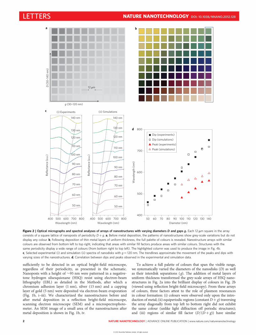
sufficiently to be detected in an optical bright-field microscope,regardless of their periodicity, as presented in the schematic.Nanoposts with a height of �95 nm were patterned in a negative-tone hydrogen silsesquioxane (HSQ) resist using electron-beamlithography (EBL) as detailed in the Methods, after which achromium adhesion layer (1 nm), silver (15 nm) and a cappinglayer of gold (5 nm) were deposited via electron-beam evaporation(Fig. 1b, i–iii). We characterized the nanostructures before andafter metal deposition in a reflection bright-field microscope,scanning electron microscope (SEM) and a microspectrophoto-meter. An SEM image of a small area of the nanostructures aftermetal deposition is shown in Fig. 1b, iv.
To achieve a full palette of colours that span the visible range,we systematically varied the diameters of the nanodisks (D) as wellas their interdisk separations ( g). The addition of metal layers ofuniform thickness transformed the grey-scale arrays of HSQ nano-structures in Fig. 2a into the brilliant display of colours in Fig. 2b(viewed using reflection bright-field microscopy). From these arraysof colours, three factors attest to the role of plasmon resonancesin colour formation: (i) colours were observed only upon the intro-duction of metal; (ii) equiperiodic regions (constant Dþ g) traversingthe array diagonally from top left to bottom right did not exhibitthe same colour (unlike light diffraction off periodic structures);and (iii) regions of similar fill factor (D/(Dþ g)) have similar
Wav
elen
gth
(nm
)
Diameter (nm)
800
700
600
500
40050 60 70 80 90 100 110 120 130 140
140 nm
Refle
ctan
ce (a
.u.)
Refle
ctan
ce (a
.u.)
140 nm
130 nm 130 nm
100 nm
60 nm
90 nm
70 nm
50 nm
400 500 600 700 800Wavelength (nm)
400 500 600 700 800Wavelength (nm)
80 nm
120 nm
110 nm 110 nm
120 nm
60 nm
70 nm
80 nm
90 nm
100 nm
50 nm
(i) Experiments (ii) Simulations
Dip (experiments)
Dip (simulations)
Peak (simulations)
Peak (experiments)
b
D (5
0–14
0 nm
)
a
d
c
12 µm
g (30–120 nm)
Figure 2 | Optical micrographs and spectral analyses of arrays of nanostructures with varying diameters D and gaps g. Each 12mm square in the array
consists of a square lattice of nanoposts of periodicity Dþ g. a, Before metal deposition, the patterns of nanostructures show grey-scale variations but do not
display any colour. b, Following deposition of thin metal layers of uniform thickness, the full palette of colours is revealed. Nanostructure arrays with similar
colours are observed from bottom left to top right, indicating that areas with similar fill factors produce areas with similar colours. Structures with the
same periodicity display a wide range of colours (from bottom right to top left). The highlighted column was used to produce the image in Fig. 4b.
c, Selected experimental (i) and simulation (ii) spectra of nanodisks with g¼ 120 nm. The trendlines approximate the movement of the peaks and dips with
varying sizes of the nanostructures. d, Correlation between dips and peaks observed in the experimental and simulation data.
LETTERS NATURE NANOTECHNOLOGY DOI: 10.1038/NNANO.2012.128
NATURE NANOTECHNOLOGY | ADVANCE ONLINE PUBLICATION | www.nature.com/naturenanotechnology2
© 2012 Macmillan Publishers Limited. All rights reserved.

colours (most noticeably in the dark band going from bottom left tomid right of the array), in accordance with the plasmon resonancesoperating close to the quasi-static limit28, where retardation effectsare minimal and resonances are independent of size scaling.
Figure 2c, i presents spectral analyses of the rightmost column inthe array (indicated by a blue box), with the spectra exhibiting peaksand dips that could be tuned across the visible spectrum by varyingD and thus the periodicity Dþ g (see Supplementary Fig. S2 forexperimental spectra of other D, g values). Simulations (Fig. 2c, ii)demonstrate qualitative agreement with the correspondingexperimental results, as is further exemplified in Fig. 2d, whereboth peaks (triangles) and dips (squares) redshift with increasingD (ref. 29). Through simulations, a subtle difference is found inthe origin of the spectral dips for D , 100 nm when comparedwith larger disks (Supplementary Fig. S3). The dips for smallerdisks are due to power absorption by the disks and, to a lesserextent, the backreflector. Together, the disk, post and backreflectoreffectively act as an antireflection stack at this wavelength(Supplementary Fig. S3c, iii and d, iii). Conversely, the dips forlarger disks are due to Fano resonances that result from the interfer-ence between the broad resonance of the nanoholes and nanodiskswith the sharp resonance of the surface modes19,20. At this resonancecondition, optical power flows around the nanodisks, through thenanoholes, and is absorbed by the backreflector/silicon substrate(see the Poynting vector plots in Supplementary Fig. S3d, ii). Thepeaks correspond to the plasmon resonances of the disks, whichintensify for larger disks because of their increased scatteringstrengths30 (Supplementary Fig. S4).
It is well known that the periodicity of nanoholes in a metal filmdetermines its optical resonance10,11, but it is less obvious how struc-tures with a constant periodicity can produce a range of colours.Figure 3 presents simulation results for structures with a constantperiodicity of 120 nm and D varying between 50 nm and 90 nm,which exhibit multiple colours as indicated in the insets ofFig. 3a. Simulations of the three different configurations shown inFig. 3a indicate that structures comprising only nanodisks or only
a backreflector plane cannot produce the colours observed. The met-allic backreflector alone (dotted lines) displays a fairly constant spec-trum across arrays with the same periodicity, with a point of inflexionat 900 nm, the signature of a Fano resonance profile20, and a dip at�450 nm that is attributable to the antireflection stack at this wave-length, as described earlier. Evidence for the dip at �450 nmhaving a different physical origin from the feature at 900 nm can beseen in its invariance to changing periodicity (SupplementaryFig. S5). For structures with just disks (dashed lines), a single peakis observed corresponding to the nanodisk plasmon resonance thatblueshifts and intensifies with increasing D only within a narrow spec-tral range between l¼ 570 nm and 590 nm. A span of colours isachieved only in the combined structure; as the scattering strengthof the disks increases, the spectrum peak shifts in favour of the nano-disk resonance and away from the Fano resonance. Simulations(Supplementary Fig. S6) indicate that structures consisting of disksraised above a backreflector film without nanoholes would displaysimilar colours but without the Fano resonance. However, the effectof Fano resonance in our system, although non-crucial, aids in nar-rowing the main spectral peaks for purer colours.
Figure 3b demonstrates the electric field enhancement and showsthe Poynting vector plots for the combined structure extracted at (i)450 nm, (ii) 590 nm and (iii) 900 nm for D¼ 90 nm. The nanodiskappears to play different roles at each of these wavelengths: it isabsorbing in the antireflection stack in (i), scattering in (ii) andenhancing absorption around the nanohole in (iii). These effectscan also be seen in the channelling of the Poynting vectors intothe nanodisk in (i), the strong fields signifying nanodisk plasmonresonance in (ii), and the directing of power flow around thenanodisk and into the base of the nanohole in (iii). The decreasedreflectance at l¼ 900 nm compared to that of the backreflectoralone is evidence that the nanodisk acts as an antenna that enhancesthe absorption around the nanohole23.
We now present the fabrication of microscopic colour images todemonstrate the creation of arbitrary images with colour and tonalcontrol. The creation of a photo-realistic image is demonstrated in
(ii)a
0
5
(i) 450 nmD = 90
D = 80
D = 70
D = 60
D = 50
400 600 800
5
4
3
Refle
ctan
ce (a
.u.)
2
1
01,000
Wavelength (nm)
5
0z
y
b
(i) (iii) (ii) 590 nm (iii) 900 nm
E/Einc
S/Sinc
Figure 3 | Numerical simulation for structures of the same periodicity (D 1 g 5 120 nm). a, Simulated reflectance spectra plots for structures with varying
D. The corresponding experimentally observed colour is shown in the squares. Solid lines show reflectances for the combined structure (with disks and
backreflector), dotted lines for the case where metal nanodisks are removed, and dashed lines for the case where the backreflector is removed. Note that the
feature corresponding to a Fano resonance occurs at a constant wavelength of �900 nm for all values of D. Colour variation at constant periodicity can be
achieved only for the combined structure of nanodisks and backreflector. b, Electric field enhancement plots (top) and time-averaged power flow vector plots
(bottom) for a single repeat structure with D¼ 90 nm at wavelengths of 450 nm (i), 590 nm (ii) and 900 nm (iii). Electric field enhancement calculated as
electric field (E) divided by the incident field (Einc), and the power flow vectors (S) were normalized by the incident Poynting vector (Sinc). Plane wave
illumination is incident from above in the z-direction and polarized along the y-axis. The spectral dip at 450 nm in a corresponds to light being absorbed by
both the metal structures and silicon substrate. The peak at 590 nm is due to plasmon resonance of the disk acting as a dipole antenna that re-radiates light
back to the observer. The inflexion point at 900 nm signifies a resonance where power flows around the disk, through the nanohole, and is absorbed by the
bottom rim of the nanohole array and substrate.
NATURE NANOTECHNOLOGY DOI: 10.1038/NNANO.2012.128 LETTERS
NATURE NANOTECHNOLOGY | ADVANCE ONLINE PUBLICATION | www.nature.com/naturenanotechnology 3
© 2012 Macmillan Publishers Limited. All rights reserved.

the 50 × 50 mm square Lena image (previously presented as aminiaturized grey-scale image31) shown in Fig. 4a–c. Colour infor-mation from bitmap images was coded pixel by pixel into the pos-ition, diameter (D) and separation ( g) of nanoposts formed in theHSQ resist (for details see Supplementary Figs S7,S8). For thisdemonstration, the pixel was a 250 × 250 nm square (that is, atthe theoretical resolution limit of the optical microscope, ×100objective, numerical aperture (NA)¼ 0.9, mid-spectrum wave-length of 500 nm; see http://www.microscopyu.com/articles/for-mulas/formulasresolution.html). Most pixels consisted of fournanodisks, as shown schematically in Fig. 1b, ii, although singlenanodisks were also used to achieve the blue/purple colours.The colour information latent in the grey-scale structures(Fig. 4a) manifested upon deposition of the metal layers(Fig. 4b). Remarkably, the resulting image closely reproduces thedetails of the original image down to single-pixel elements, asseen in the appearance of specular reflections in the eyes(Fig. 4c). The accompanying SEM micrograph in Fig. 4c showsthe structures, which have the same centre-to-centre periodicitybut different D and g. This image is enlarged from the region indi-cated in Fig. 4c, which consists of four different colours.
To demonstrate the colour pixel resolution at the optical diffractionlimit, we patterned a set of chequerboard resolution test structureswith alternating colours. As shown in Fig. 4d,e, each square in the che-querboard consists of a 3 × 3 (Fig. 4d) or 2 × 2 (Fig. 4e) array of disksper pixel. The centre-to-centre separation of the disks is 125 nm,matching that of Fig. 4a–c. Although the number of disks per pixelis reduced from nine to four disks in Fig. 4e, the colour scheme ofeach chequerboard is preserved. The fact that the individual coloursare just resolved by a diffraction-limited optical microscope indicatesthat the single pixels of four nanodisks were indeed able to supportindividual colours at the optical diffraction limit.
The critical advantage of this approach is that the colour infor-mation latent in the resist structures can be replicated economically
onto multiple substrates using high-throughput methods (such asNIL; Supplementary Fig. S9) once a master mould is fabricated.In addition to achieving high resolution, the use of plasmonic reso-nators also provides secondary degrees of freedom to colour cre-ation, including polarization dependence17. We anticipate thatfurther improvements in resolution and colour perception will beachieved by using different geometries and/or smaller numbers ofnanostructures per pixel area.
In summary, we have presented an approach for full-colourprinting at the optical diffraction limit by encoding colour infor-mation into silver/gold nanodisks raised above a holey backreflec-tor. The interplay of plasmon and Fano resonances, which can betuned by varying the size and separation of the nanodisks, resultsin colours directly visible under a bright-field optical microscope.These colours are preserved even when only four disks are presentin individual pixels of 250 × 250 nm squares, thus enablingcolour printing at a resolution of �100,000 d.p.i. This printing res-olution brings us to the limit of visible-light imaging, where theindividual colour pixels are just barely resolvable usingdiffraction-limited optics. Beyond obvious applications in high-res-olution print image production, this method can also be used inoptical data storage and colour filters in lighting andimaging technologies.
MethodsElectron-beam lithography. The figures in the main text show colour informationencoded into the dimension and position of nanostructures by EBL. The negative-tone electron-beam resist HSQ (formulated as product number XR-1541-006, DowCorning) was spin-coated onto silicon substrates to a thickness of 95 nm. To avoidthermally induced crosslinking of the resist, which would reduce its resolution, nobaking process was used. A computer-generated layout consisting of arrays of diskswith a range of nominal diameters (50–140 nm) and gaps (30–120 nm) wasdesigned. EBL was performed using an Elionix ELS-7000 EBL system with anaccelerating voltage of 100 kV and a beam current of 500 pA. The write field was set to150 mm × 150 mm and the exposure step size was 2.5 nm. The dose used for thenanodisk structures was 12 mC cm22. No proximity-effect correction was performed
b a
d e
c
Figure 4 | Full-colour image printing and resolution test patterns. a,b, Optical micrographs of the Lena image before (a) and after (b) metal deposition.
c, Optical micrograph of an enlarged region of the image, showing the remarkable detail and colour rendition on a micrometre-scale level. The accompanying
SEM image of the indicated region shows that the nanostructures that make up the image have a similar periodicity of 125 nm but exhibit different colours in
the optical image due to a small (30 nm) variation in nanodisk sizes. For clarity, the individual regions of similarly sized disks are separated by the dotted
lines. Each pixel consists of a 2 × 2 array of disks with a pitch of 250 nm. d,e, Resolution test patterns in the form of chequerboards approaching (d) and at
(e) the optical diffraction limit. In d, a set of chequerboards consists of a combination of two colours, one darker than the other. Each square of the
chequerboard is 375 nm in size and consists of an array of 3 × 3 structures, as shown in the corresponding SEM image. In e a similar chequerboard with
colour squares of 250 nm (with the size of pixels used in the Lena image) consists of an array of 2 × 2 structures, as shown in the SEM image.
The chequerboard pattern is only barely observable, even with a ×150 and 0.9 NA objective, demonstrating the patterning of colour pixels at the
optical diffraction limit. Scale bars: 10mm (a, b), 1 mm (c), 500 nm (d, e).
LETTERS NATURE NANOTECHNOLOGY DOI: 10.1038/NNANO.2012.128
NATURE NANOTECHNOLOGY | ADVANCE ONLINE PUBLICATION | www.nature.com/naturenanotechnology4
© 2012 Macmillan Publishers Limited. All rights reserved.

for the exposure. Instead, to achieve well-defined nanodisk structures with steepsidewalls, a high-contrast development process32 was used by developing samples in aformulation of aqueous 1% NaOH, 4% NaCl in deionized (DI) water at 24 8C for1 min, followed by rinsing under running DI water for 2 min, and isopropyl alcohol(IPA). Finally, the samples were blow-dried under a steady stream of N2.
Nanoimprint lithography. Supplementary Fig. S8 shows the scaling up of colourproduction over large areas using NIL as a means for creating the disknanostructures. The nanoimprint process was performed in an Obducat Sindre600 thermal nanoimprinting system. A silicon mould (NIL Technology) with ananohole array (diameter, 100 nm; pitch, 200 nm; depth, 100 nm) occupying an areaof 1 cm × 1 cm was used as the mould to produce a large-area nanopost array. Thesubstrate for the nanoimprint was a 2 cm × 2 cm polycarbonate film with a thicknessof 125 mm. Before the imprinting process, the silicon mould was cleaned and a self-assembled monolayer of 1H,1H,2H,2H-perflourodecyltrichlorosilane (FDTS) anti-stiction coating was functionalized on the surface. This layer was necessary fordetachment of the mould from the imprinted substrate in the subsequent process.The imprinting process was carried out at 150 8C under a pressure of 40 bar. Thiscondition was maintained for 300 s, after which the system was cooled to 30 8Cbefore manual detachment of the silicon mould from the imprintedpolycarbonate film.
Metal deposition. Metal deposition was performed using an electron-beamevaporator (Explorer Coating System, Denton Vacuum). A chromium adhesionlayer (1 nm), a silver plasmon-active layer (15 nm) and a gold capping layer (5 nm)were sequentially deposited onto the samples. All metals were deposited at a rate of1Ås21. The chromium adhesion layer was necessary to provide scratch resistance inthe resulting metal layers and had minimal effect on the optical properties of thestructures. The gold capping layer hindered the sulphidation of silver. The workingpressure during evaporation was �1 × 1026 torr. The temperature of the samplechamber was maintained at 20 8C during the entire evaporation process, with thesample holder rotating at a rate of 50 r.p.m. to ensure uniformity of the deposition.
The fabricated structures were imaged using an Elionix ESM-9000 scanningelectron microscope with an accelerating voltage of 10 kV and a working distanceof 5 mm.
Optical measurements. To investigate the optical properties of the fabricatedstructures, extinction spectra were measured in reflection mode using a QDI 2010UV-visible-NIR range microspectrophotometer (CRAIC Technology). Bothincident and collected light were at normal incidence to the substrate, with theelectric field of the unpolarized light in plane with the substrate surface. Opticalmicrographs were acquired using a Nikon MM-40/L3FA (Nikon) set-up with a×100, 0.9 NA air objective as well as with a Olympus MX61 set-up with ×150,0.9 NA air objective, using a JVC Colour Video Camera TKC14-81EG (JVC Corp)for the former and an SC30 Olympus Digital Camera for the latter.
Numerical simulations. Simulations of the reflectance spectra were carried outusing a frequency domain solver from the Computer Simulation Technology(CST AG) microwave studio commercial software. Unit-cell boundaries were used inthe plane of the disks and Floquet ports were used for terminating the domain in thedirection of incidence. The frequency-domain solver incorporated measuredwavelength dispersion of the permittivity of the various materials used in thestructure (data for silicon, gold and silver were taken from ref. 33 and HSQ wassimulated using a constant refractive index of 1.4).
Received 2 April 2012; accepted 29 June 2012;published online 12 August 2012
References1. Finlayson, C. E. et al. 3D bulk ordering in macroscopic solid opaline films by
edge-induced rotational shearing. Adv. Mater. 23, 1540–1544 (2011).2. Haverinen, H. M., Myllylae, R. A. & Jabbour, G. E. Inkjet printing of light
emitting quantum dots. Appl. Phys. Lett. 94, 073108 (2009).3. Kim, T-H. et al. Full-colour quantum dot displays fabricated by transfer
printing. Nature Photon. 5, 176–182 (2011).4. Lee, S. Y. et al. Plasmon-enhanced structural coloration of metal films with
isotropic pinwheel nanoparticle arrays. Opt. Express 19, 23818–23830 (2011).5. Ozaki, M., Kato, J. & Kawata, S. Surface-plasmon holography with white-light
illumination. Science 332, 218–220 (2011).6. Xu, T., Wu, Y-K., Kaplan, A. F., Ok, J. G. & Guo, J. L. Structural colors: from
plasmonic to carbon nanostructures. Small 7, 3128–3136 (2011).7. Ahn, S. H. & Guo, L. J. High-speed roll-to-roll nanoimprint lithography on
flexible plastic substrates. Adv. Mater. 20, 2044–2049 (2008).8. Kustandi, T. S., Low, H. Y., Teng, J. H., Rodriguez, I. & Yin, R. Mimicking domino-
like photonic nanostructures on butterfly wings. Small 5, 574–578 (2009).9. Javidi, B. Optical and Digital Techniques for Information Security
(Springer, 2005).
10. Chen, Q. & Cumming, D. R. High transmission and low color cross-talkplasmonic color filters using triangular-lattice hole arrays in aluminum films.Opt. Express 18, 14056–14062 (2010).
11. Inoue, D. et al. Polarization independent visible color filter comprising analuminum film with surface-plasmon enhanced transmission through asubwavelength array of holes. Appl. Phys. Lett. 98, 093113 (2011).
12. Xu, T., Wu, Y-K., Luo, X. & Guo, J. L. Plasmonic nanoresonators for high-resolution colour filtering and spectral imaging. Nature Commun. 1, 1–5 (2010).
13. Abbe, E. A contribution to the theory of the microscope and the nature ofmicroscopic vision. Proc. Bristol Nat. Soc. 1, 200–261 (1874).
14. Huang, J., Wang, X. & Wang, Z. L. Controlled replication of butterfly wings forachieving tunable photonic properties. Nano Lett. 6, 2325–2331 (2006).
15. Huo, F. et al. Polymer pen lithography. Science 321, 1658–1660 (2008).16. Piner, R. D., Zhu, J., Xu, F., Hong, S. & Mirkin, C. A. ‘Dip-pen’ nanolithography.
Science 283, 661–663 (1999).17. Ellenbogen, T., Seo, K. & Crozier, K. B. Chromatic plasmonic polarizers for
active visible color filtering and polarimetry. Nano Lett. 12, 1026–1031 (2012).18. Laux, E., Genet, C., Skauli, T. & Ebbesen, T. W. Plasmonic photon sorters for
spectral and polarimetric imaging. Nature Photon. 2, 161–164 (2008).19. Liu, H. & Lalanne, P. Microscopic theory of the extraordinary optical
transmission. Nature 452, 728–731 (2008).20. Luk’yanchuk, B. et al. The Fano resonance in plasmonic nanostructures and
metamaterials. Nature Mater. 9, 707–715 (2010).21. Ebbesen, T. W., Lezec, H. J., Ghaemi, H. F., Thio, T. & Wolff, P. A. Extraordinary
optical transmission through sub-wavelength hole arrays. Nature 391,667–669 (1998).
22. Li, W-D., Ding, F., Hu, J. & Chou, S. Y. Three-dimensional cavity nanoantennacoupled plasmonic nanodots for ultrahigh and uniform surface-enhancedRaman scattering over large area. Opt. Express 19, 3925–3936 (2011).
23. Li, W-D., Hu, J. & Chou, S. Y. Extraordinary light transmission through opaquethin metal film with subwavelength holes blocked by metal disks. Opt. Express19, 21098–21108 (2011).
24. Liu, Y. J. et al. Optically tunable plasmonic color filters. Appl. Phys. A 107,49–54 (2011).
25. Caldwell, J. D. et al. Plasmonic nanopillar arrays for large-area, high-enhancementsurface-enhanced Raman scattering sensors. ACS Nano 5, 4046–4055 (2011).
26. Chanda, D. et al. Coupling of plasmonic and optical cavity modes in quasi-three-dimensional plasmonic crystals. Nature Commun. 2, 1–7 (2011).
27. Wells, S. M., Polemi, A., Lavrik, N. V., Shuford, K. L. & Sepaniak, M. J. Efficientdisc on pillar substrates for surface enhanced Raman spectroscopy. Chem.Commun. 47, 3814–3816 (2011).
28. Maier, S. A. Plasmonics: Fundamentals and Applications (Springer, 2007).29. Jain, P. K., Lee, K. S., El-Sayed, I. H. & El-Sayed, M. A. Calculated absorption and
scattering properties of gold nanoparticles of different size, shape, andcomposition: applications in biological imaging and biomedicine. J. Phys. Chem.B 110, 7238–7248 (2006).
30. Mie, G. Contributions to the optical characteristis of turbid tubes, particularly ofcolloidal metal solutions (beitraege zur optik trueber Medien, speziell kolloidalerMetalloesungen). Ann. Phys. 25, 377–445 (1908).
31. Yang, J. K. W., Duan, H., Law, J. B. K., Low, H. Y. & Cord, B. Miniaturization ofgrayscale images. J. Vac. Sci. Technol. B 29, 06F313 (2011).
32. Yang, J. K. W. & Berggren, K. K. Using high-contrast salty development ofhydrogen silsesquioxane for sub-10-nm half-pitch lithography. J. Vac. Sci.Technol., B 25, 2025–2029 (2007).
33. Palik, E. D. Handbook of Optical Constants of Solids Vol. 1, 386–350(Elsevier, 1998).
AcknowledgementsThis work was supported by the Agency for Science, Technology and Research (A*STAR)Young Investigatorship (grant no. 0926030138) and SERC (grant no. 092154099).The work made use of the SERC nano Fabrication, Processing and Characterization(SnFPC) facilities in IMRE. The authors thank S.H. Goh, I.Y. Phang, J. Deng and V.S.F. Limfor technical assistance, and M. Asbahi, M. Bosman, W.P. Goh and K.T.P. Lim (IMRE) andK.K. Berggren (MIT) for fruitful discussions.
Author contributionsK.K., H.D. and J.K.W.Y. conceived the ideas and designed the experiments. K.K., H.D. andJ.K.W.Y. fabricated and characterized the samples. R.S.H., S.C.W.K. and J.N.W. performednumerical simulations. All authors analysed the data and wrote the manuscript.
Additional informationSupplementary information is available in the online version of the paper. Reprints andpermission information is available online at http://www.nature.com/reprints. Correspondenceand requests for materials should be addressed to J.K.W.Y.
Competing financial interestsThe authors declare no competing financial interests.
NATURE NANOTECHNOLOGY DOI: 10.1038/NNANO.2012.128 LETTERS
NATURE NANOTECHNOLOGY | ADVANCE ONLINE PUBLICATION | www.nature.com/naturenanotechnology 5
© 2012 Macmillan Publishers Limited. All rights reserved.