Embed Size (px)
Citation preview
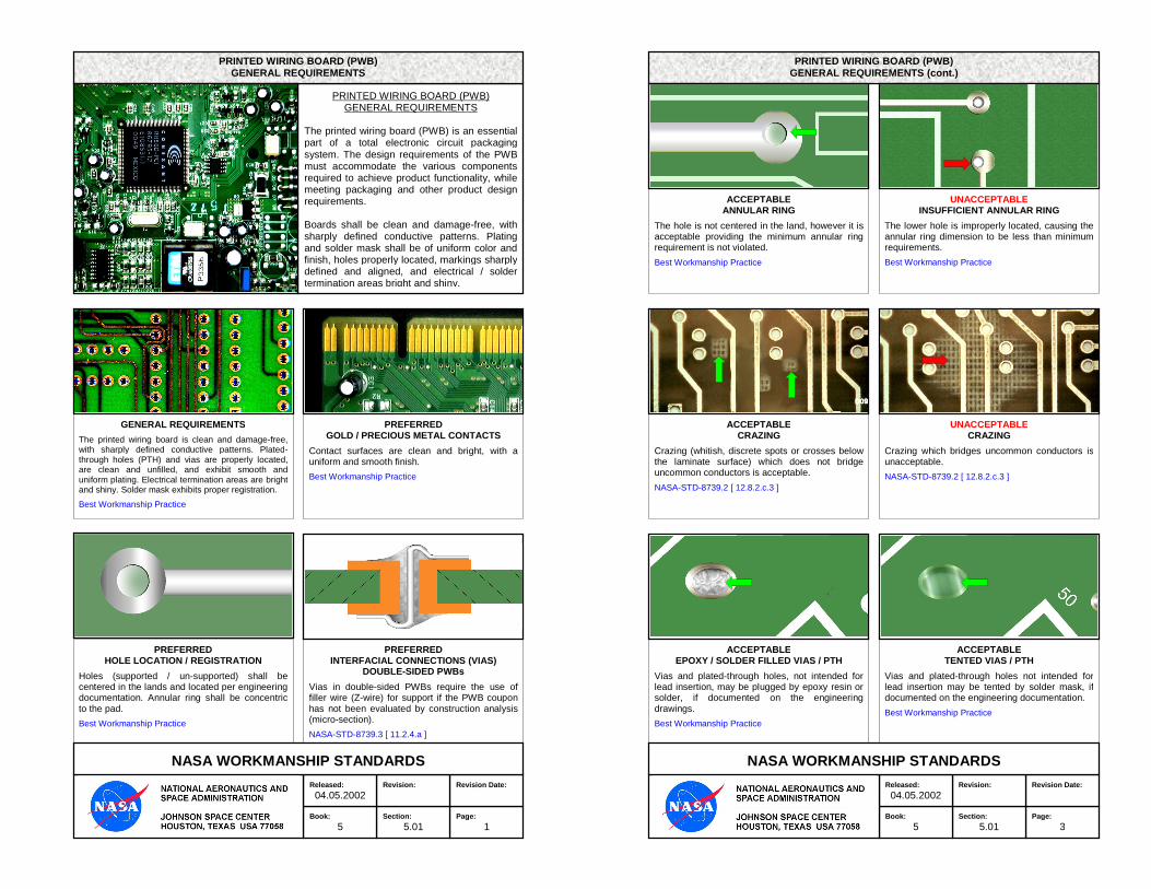
ACCEPTABLE CRAZING
Crazing (whitish, discrete spots or crosses below the laminate surface) which does not bridge uncommon conductors is acceptable.
NASA-STD-8739.2 [ 12.8.2.c.3 ]
PRINTED WIRING BOARD (PWB) GENERAL REQUIREMENTS (cont.)
PREFERRED GOLD / PRECIOUS METAL CONTACTS
Contact surfaces are clean and bright, with a uniform and smooth finish.
Best Workmanship Practice
PREFERRED HOLE LOCATION / REGISTRATION
Holes (supported / un-supported) shall be centered in the lands and located per engineering documentation. Annular ring shall be concentric to the pad.
Best Workmanship Practice
Page:
1
Revision Date:
Section:
5.01
Revision:
Book:
5
Released:
04.05.2002
GENERAL REQUIREMENTS
The printed wiring board is clean and damage-free, with sharply defined conductive patterns. Plated-through holes (PTH) and vias are properly located, are clean and unfilled, and exhibit smooth and uniform plating. Electrical termination areas are bright and shiny. Solder mask exhibits proper registration.
Best Workmanship Practice
PRINTED WIRING BOARD (PWB) GENERAL REQUIREMENTS
The printed wiring board (PWB) is an essential part of a total electronic circuit packaging system. The design requirements of the PWB must accommodate the various components required to achieve product functionality, while meeting packaging and other product design requirements. Boards shall be clean and damage-free, with sharply defined conductive patterns. Plating and solder mask shall be of uniform color and finish, holes properly located, markings sharply defined and aligned, and electrical / solder termination areas bright and shiny.
PRINTED WIRING BOARD (PWB) GENERAL REQUIREMENTS
Page:
3
Revision Date:
Section:
5.01
Revision:
Book:
5
Released:
04.05.2002
PREFERRED INTERFACIAL CONNECTIONS (VIAS)
DOUBLE-SIDED PWBs
Vias in double-sided PWBs require the use of filler wire (Z-wire) for support if the PWB coupon has not been evaluated by construction analysis (micro-section).
NASA-STD-8739.3 [ 11.2.4.a ]
UNACCEPTABLE INSUFFICIENT ANNULAR RING
The lower hole is improperly located, causing the annular ring dimension to be less than minimum requirements.
Best Workmanship Practice
ACCEPTABLE
ANNULAR RING
The hole is not centered in the land, however it is acceptable providing the minimum annular ring requirement is not violated.
Best Workmanship Practice
UNACCEPTABLE CRAZING
Crazing which bridges uncommon conductors is unacceptable.
NASA-STD-8739.2 [ 12.8.2.c.3 ]
ACCEPTABLE EPOXY / SOLDER FILLED VIAS / PTH
Vias and plated-through holes, not intended for lead insertion, may be plugged by epoxy resin or solder, if documented on the engineering drawings.
Best Workmanship Practice
ACCEPTABLE TENTED VIAS / PTH
Vias and plated-through holes not intended for lead insertion may be tented by solder mask, if documented on the engineering documentation.
Best Workmanship Practice
NASA WORKMANSHIP STANDARDS NASA WORKMANSHIP STANDARDS
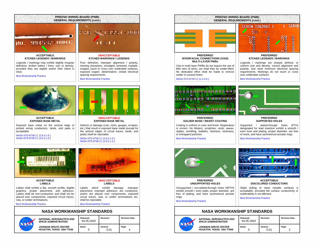
PREFERRED INTERFACIAL CONNECTIONS (VIAS)
MULTI-LAYER PWBs
Vias in multi-layer PWBs do not require the use of filler wire (Z-wire), nor shall they be solder-filled. No dedicated effort shall be made to remove solder in unused holes.
NASA-STD-8739.3 [ 11.2.4.b ]
PREFERRED ETCHED LEGENDS / MARKINGS
Legends / markings are sharply defined, of uniform size and density, correct alignment and polarity, and meet minimum electrical spacing requirements. Markings do not touch or cross over solderable surfaces.
Best Workmanship Practice
PREFERRED SOLDER MASK / RESIST COATING
Coating is uniform in color and finish. Registration is correct. No blisters, scratches, voids, waves, ripples, wrinkling, bubbles, haziness, tackiness, or entrapped particles.
Best Workmanship Practice
PREFERRED SUPPORTED HOLES
Supported / plated-through holes (PTH) designated for lead insertion exhibit a smooth / even bore and plating, proper diameter, are free of resist, and have symmetrical annular rings.
Best Workmanship Practice
PREFERRED UNSUPPORTED HOLES
Unsupported / non-plated-through holes (NPTH) exhibit smooth / even walls, proper diameter, are free of plating, and have symmetrical annular rings.
Best Workmanship Practice
Revision:
Page:
4
Revision Date:
Book:
5
Released:
04.05.2002
Section:
5.01
Section:
5.01
Revision:
Page:
2
Revision Date:
Book:
5
Released:
04.05.2002
PRINTED WIRING BOARD (PWB) GENERAL REQUIREMENTS (cont.)
PRINTED WIRING BOARD (PWB) GENERAL REQUIREMENTS (cont.)
ACCEPTABLE DISCOLORED CONDUCTORS
Slight dulling of clean metallic surfaces is acceptable, provided the surface conductivity or solderability is not affected.
Best Workmanship Practice
NASA WORKMANSHIP STANDARDS
UNACCEPTABLE EXPOSED BASE METAL
Defects or damage (cuts, nicks, gouges, scrapes, etc.) that result in exposed base metal (except for the vertical edges of circuit traces, lands, and pads) shall be rejectable.
NASA-STD-8739.2 [ 12.8.2.c.5 ] NASA-STD-8739.3 [ 13.6.2.c.5 ]
ACCEPTABLE EXPOSED BASE METAL
Exposed base metal on the vertical edge of printed wiring conductors, lands, and pads is acceptable.
NASA-STD-8739.2 [ 12.8.2.c.5 ] NASA-STD-8739.3 [ 13.6.2.c.5 ]
ACCEPTABLE ETCHED LEGENDS / MARKINGS
Legends / markings may exhibit slightly irregular definition, broken letters / lines, size or density, provided they are legible and/or their intent is clear.
Best Workmanship Practice
UNACCEPTABLE
ETCHED MARKINGS / LEGENDS
Poor definition, improper alignment / polarity, missing characters, smudged, smeared, multiple-imaged, touch or cross over solderable surfaces, exposed copper, delamination, violate electrical spacing requirements.
Best Workmanship Practice
ACCEPTABLE LABELS
Labels shall exhibit a flat, smooth profile, legible graphics, proper placement, and adhesion. Labels shall be non-conductive, and shall not be placed over components, exposed circuit traces, vias, or solder terminations.
Best Workmanship Practice
UNACCEPTABLE LABELS
Labels which exhibit damage, improper placement, improper adhesion, are conductive, and/or are placed over components, exposed circuit traces, vias, or solder terminations etc. shall be rejectable.
Best Workmanship Practice
NASA WORKMANSHIP STANDARDS
Page:
5
Revision Date:
Section:
5.01
Revision:
Book:
5
Released:
04.05.2002
Page:
7
Revision Date:
Section:
5.01
Revision:
Book:
5
Released:
04.05.2002
PRINTED WIRING BOARD (PWB) GENERAL REQUIREMENTS (cont.)
PRINTED WIRING BOARD (PWB) GENERAL REQUIREMENTS (cont.)
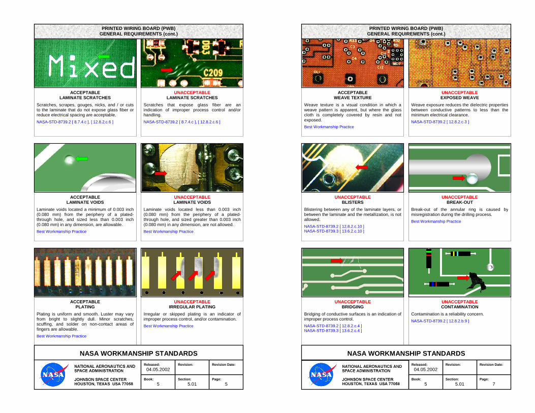
UNACCEPTABLE LAMINATE SCRATCHES
Scratches that expose glass fiber are an indication of improper process control and/or handling.
NASA-STD-8739.2 [ 8.7.4.c ], [ 12.8.2.c.6 ]
ACCEPTABLE
LAMINATE SCRATCHES
Scratches, scrapes, gouges, nicks, and / or cuts to the laminate that do not expose glass fiber or reduce electrical spacing are acceptable.
NASA-STD-8739.2 [ 8.7.4.c ], [ 12.8.2.c.6 ]
ACCEPTABLE PLATING
Plating is uniform and smooth. Luster may vary from bright to slightly dull. Minor scratches, scuffing, and solder on non-contact areas of fingers are allowable.
Best Workmanship Practice
UNACCEPTABLE IRREGULAR PLATING
Irregular or skipped plating is an indicator of improper process control, and/or contamination.
Best Workmanship Practice
NASA WORKMANSHIP STANDARDS
ACCEPTABLE LAMINATE VOIDS
Laminate voids located a minimum of 0.003 inch (0.080 mm) from the periphery of a plated-through hole, and sized less than 0.003 inch (0.080 mm) in any dimension, are allowable.
Best Workmanship Practice
UNACCEPTABLE LAMINATE VOIDS
Laminate voids located less than 0.003 inch (0.080 mm) from the periphery of a plated-through hole, and sized greater than 0.003 inch (0.080 mm) in any dimension, are not allowed.
Best Workmanship Practice
ACCEPTABLE WEAVE TEXTURE
Weave texture is a visual condition in which a weave pattern is apparent, but where the glass cloth is completely covered by resin and not exposed.
Best Workmanship Practice
UNACCEPTABLE EXPOSED WEAVE
Weave exposure reduces the dielectric properties between conductive patterns to less than the minimum electrical clearance.
NASA-STD-8739.2 [ 12.8.2.c.3 ]
UNACCEPTABLE BLISTERS
Blistering between any of the laminate layers, or between the laminate and the metallization, is not allowed.
NASA-STD-8739.2 [ 12.8.2.c.10 ] NASA-STD-8739.3 [ 13.6.2.c.10 ]
UNACCEPTABLE BREAK-OUT
Break-out of the annular ring is caused by misregistration during the drilling process.
Best Workmanship Practice
UNACCEPTABLE BRIDGING
Bridging of conductive surfaces is an indication of improper process control.
NASA-STD-8739.2 [ 12.8.2.c.4 ] NASA-STD-8739.3 [ 13.6.2.c.4 ]
UNACCEPTABLE CONTAMINATION
Contamination is a reliability concern.
NASA-STD-8739.2 [ 12.8.2.b.9 ]
NASA WORKMANSHIP STANDARDS
UNACCEPTABLE SCRATCHES (PRINTED WIRING)
Scratches that expose base metal are an indication of improper process control and/or handling.
NASA-STD-8739.2 [ 12.8.2.c.5 ]
Section:
5.01
Revision:
Revision:
Page:
8
Revision Date:
Book:
5
Released:
04.05.2002
Page:
6
Revision Date:
Book:
5
Released:
04.05.2002
Section:
5.01
PRINTED WIRING BOARD (PWB) GENERAL REQUIREMENTS (cont.)
PRINTED WIRING BOARD (PWB) GENERAL REQUIREMENTS (cont.)
ACCEPTABLE MEASLING
Measling (whitish, discrete spots or crosses) below the laminate surface that do not bridge uncommon conductors is acceptable.
NASA-STD-8739.2 [ 12.8.2.c.3 ]
UNACCEPTABLE MEASLING
Measling (whitish, discrete spots or crosses below the laminate surface) which bridges uncommon conductors is unacceptable.
NASA-STD-8739.2 [ 12.8.2.c.3 ]
ACCEPTABLE SMOOTH TOOL IMPRESSION MARKS
Scratches, scrapes, gouges, nicks, and / or cuts to the printed wiring pattern that do not expose base metal or reduce cross-sectional area are acceptable.
NASA-STD-8739.2 [ 12.8.2.c.5 ]
UNACCEPTABLE SOLDER MASK DEFECTS
Solder mask tackiness, cracking, flaking, or separation from the substrate or conductors.
NASA-STD-8739.2 [ 12.8.2.c.8 ] NASA-STD-8739.3 [ 13.6.2.c.8 ]
ACCEPTABLE SOLDER MASK
Minor waves, ripples, or wrinkling which do not reduce the coating below minimum thickness requirements. Isolated bubbles or voids, which do not bridge conductive patterns or reduce electrical spacing requirements.
Best Workmanship Practice
NASA WORKMANSHIP STANDARDS
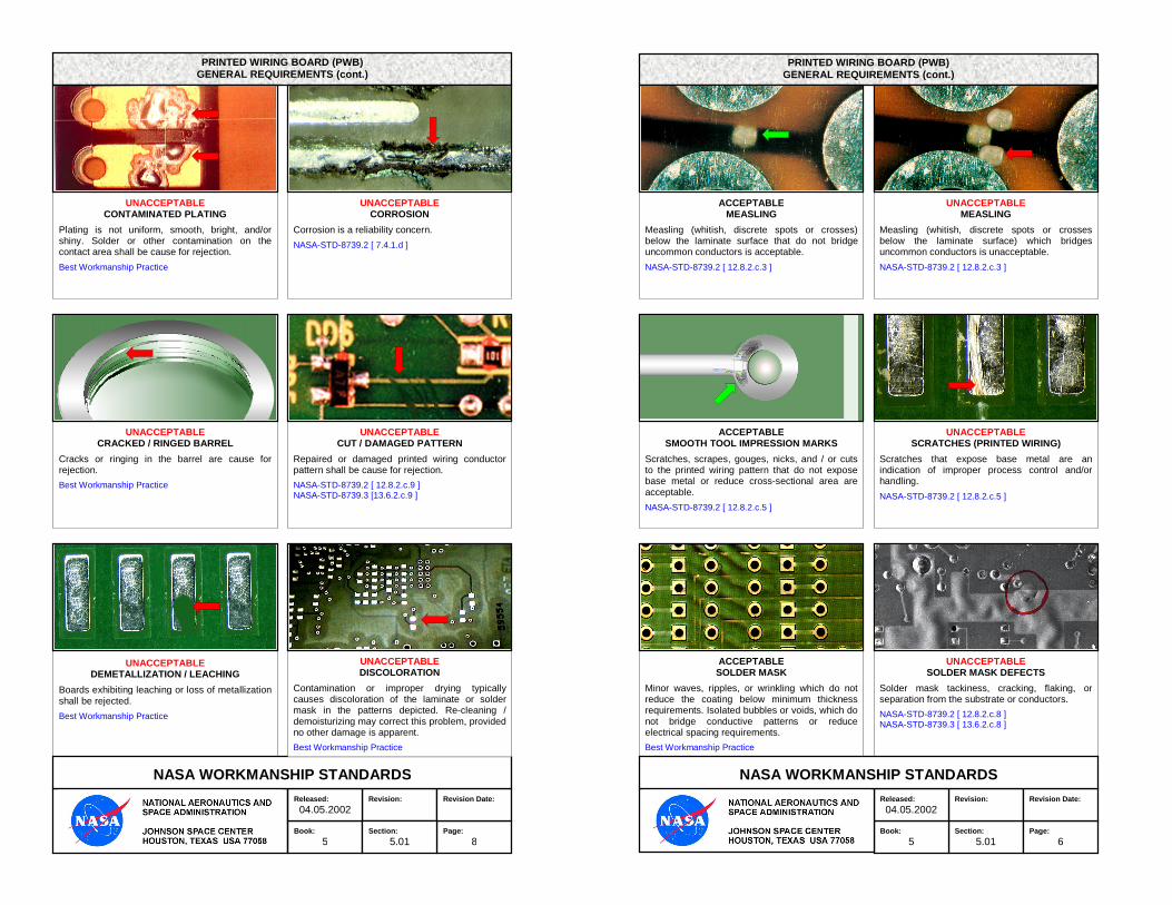
UNACCEPTABLE CONTAMINATED PLATING
Plating is not uniform, smooth, bright, and/or shiny. Solder or other contamination on the contact area shall be cause for rejection.
Best Workmanship Practice
UNACCEPTABLE CORROSION
Corrosion is a reliability concern.
NASA-STD-8739.2 [ 7.4.1.d ]
UNACCEPTABLE CRACKED / RINGED BARREL
Cracks or ringing in the barrel are cause for rejection.
Best Workmanship Practice
UNACCEPTABLE CUT / DAMAGED PATTERN
Repaired or damaged printed wiring conductor pattern shall be cause for rejection.
NASA-STD-8739.2 [ 12.8.2.c.9 ] NASA-STD-8739.3 [13.6.2.c.9 ]
UNACCEPTABLE DEMETALLIZATION / LEACHING
Boards exhibiting leaching or loss of metallization shall be rejected.
Best Workmanship Practice
NASA WORKMANSHIP STANDARDS
UNACCEPTABLE DISCOLORATION
Contamination or improper drying typically causes discoloration of the laminate or solder mask in the patterns depicted. Re-cleaning / demoisturizing may correct this problem, provided no other damage is apparent.
Best Workmanship Practice
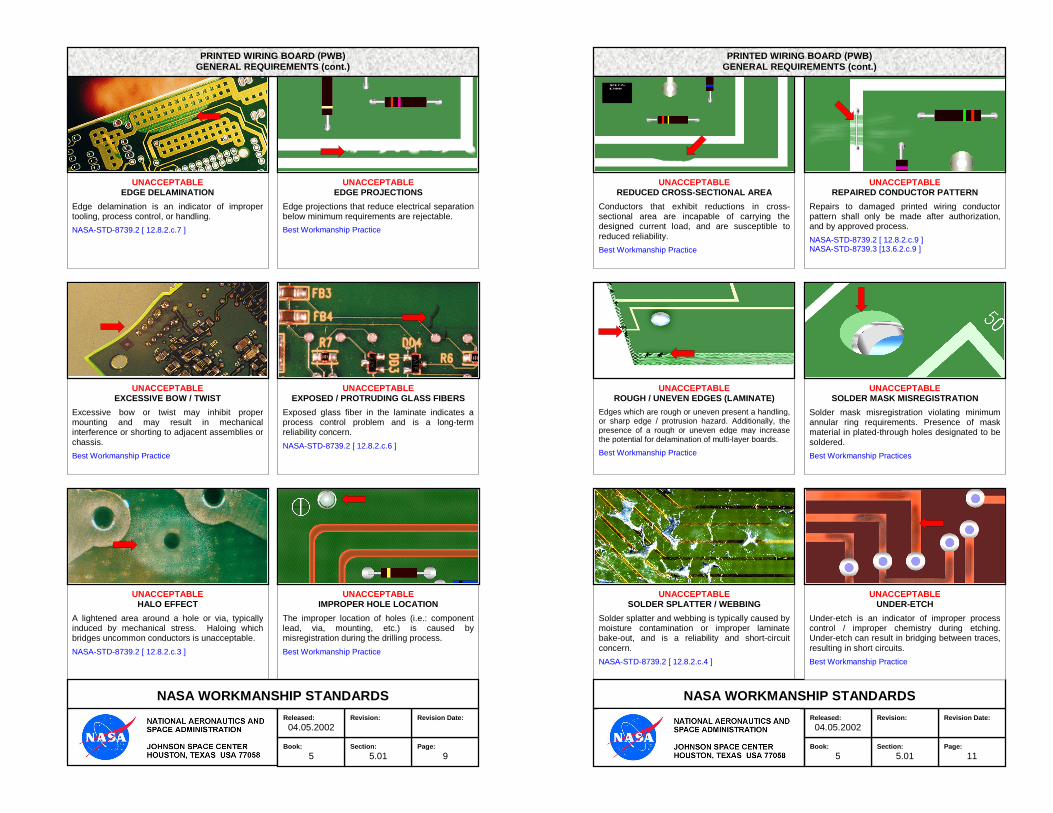
UNACCEPTABLE HALO EFFECT
A lightened area around a hole or via, typically induced by mechanical stress. Haloing which bridges uncommon conductors is unacceptable.
NASA-STD-8739.2 [ 12.8.2.c.3 ]
UNACCEPTABLE IMPROPER HOLE LOCATION
The improper location of holes (i.e.: component lead, via, mounting, etc.) is caused by misregistration during the drilling process.
Best Workmanship Practice
UNACCEPTABLE EDGE DELAMINATION
Edge delamination is an indicator of improper tooling, process control, or handling. NASA-STD-8739.2 [ 12.8.2.c.7 ]
Page:
9
Revision Date:
Section:
5.01
Revision:
Book:
5
Released:
04.05.2002
NASA WORKMANSHIP STANDARDS
Page:
11
Revision Date:
Section:
5.01
Revision:
Book:
5
Released:
04.05.2002
NASA WORKMANSHIP STANDARDS
PRINTED WIRING BOARD (PWB) GENERAL REQUIREMENTS (cont.)
PRINTED WIRING BOARD (PWB) GENERAL REQUIREMENTS (cont.)
UNACCEPTABLE REDUCED CROSS-SECTIONAL AREA
Conductors that exhibit reductions in cross-sectional area are incapable of carrying the designed current load, and are susceptible to reduced reliability.
Best Workmanship Practice
UNACCEPTABLE REPAIRED CONDUCTOR PATTERN
Repairs to damaged printed wiring conductor pattern shall only be made after authorization, and by approved process.
NASA-STD-8739.2 [ 12.8.2.c.9 ] NASA-STD-8739.3 [13.6.2.c.9 ]
UNACCEPTABLE
EDGE PROJECTIONS
Edge projections that reduce electrical separation below minimum requirements are rejectable.
Best Workmanship Practice
UNACCEPTABLE EXCESSIVE BOW / TWIST
Excessive bow or twist may inhibit proper mounting and may result in mechanical interference or shorting to adjacent assemblies or chassis.
Best Workmanship Practice
UNACCEPTABLE EXPOSED / PROTRUDING GLASS FIBERS
Exposed glass fiber in the laminate indicates a process control problem and is a long-term reliability concern.
NASA-STD-8739.2 [ 12.8.2.c.6 ]
UNACCEPTABLE ROUGH / UNEVEN EDGES (LAMINATE)
Edges which are rough or uneven present a handling, or sharp edge / protrusion hazard. Additionally, the presence of a rough or uneven edge may increase the potential for delamination of multi-layer boards.
Best Workmanship Practice
UNACCEPTABLE SOLDER MASK MISREGISTRATION
Solder mask misregistration violating minimum annular ring requirements. Presence of mask material in plated-through holes designated to be soldered.
Best Workmanship Practices
UNACCEPTABLE SOLDER SPLATTER / WEBBING
Solder splatter and webbing is typically caused by moisture contamination or improper laminate bake-out, and is a reliability and short-circuit concern.
NASA-STD-8739.2 [ 12.8.2.c.4 ]
UNACCEPTABLE UNDER-ETCH
Under-etch is an indicator of improper process control / improper chemistry during etching. Under-etch can result in bridging between traces, resulting in short circuits.
Best Workmanship Practice
Revision:
Page:
12
Revision Date:
Book:
5
Released:
04.05.2002
Section:
5.01
NASA WORKMANSHIP STANDARDS
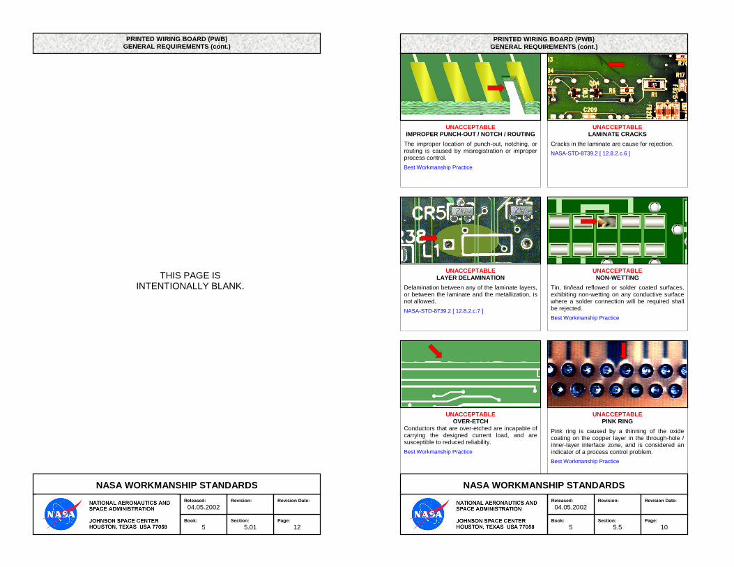
UNACCEPTABLE PINK RING
Pink ring is caused by a thinning of the oxide coating on the copper layer in the through-hole / inner-layer interface zone, and is considered an indicator of a process control problem.
Best Workmanship Practice
Section:
5.5
Revision:
Page:
10
Revision Date:
Book:
5
Released:
04.05.2002
PRINTED WIRING BOARD (PWB) GENERAL REQUIREMENTS (cont.)
PRINTED WIRING BOARD (PWB) GENERAL REQUIREMENTS (cont.)
UNACCEPTABLE IMPROPER PUNCH-OUT / NOTCH / ROUTING
The improper location of punch-out, notching, or routing is caused by misregistration or improper process control.
Best Workmanship Practice
UNACCEPTABLE
LAMINATE CRACKS
Cracks in the laminate are cause for rejection.
NASA-STD-8739.2 [ 12.8.2.c.6 ]
UNACCEPTABLE LAYER DELAMINATION
Delamination between any of the laminate layers, or between the laminate and the metallization, is not allowed.
NASA-STD-8739.2 [ 12.8.2.c.7 ]
UNACCEPTABLE NON-WETTING
Tin, tin/lead reflowed or solder coated surfaces, exhibiting non-wetting on any conductive surface where a solder connection will be required shall be rejected.
Best Workmanship Practice
UNACCEPTABLE OVER-ETCH
Conductors that are over-etched are incapable of carrying the designed current load, and are susceptible to reduced reliability.
Best Workmanship Practice
NASA WORKMANSHIP STANDARDS
THIS PAGE IS INTENTIONALLY BLANK.