Embed Size (px)
Citation preview
iCE65 Printed Circuit Board (PCB) Layout Guidelines SiliconBlue
R
February 8, 2011 (1.2) Application Note AN010
© 2009–2011 by SiliconBlue Technologies Corporation. All rights reserved. (1.2, 8-FEB-2011) www.SiliconBlueTech.com 1
Introduction
The SiliconBlue iCE65™ mobileFPGA™ family is specifically designed for small, low-power, hand-held applications. Consequently, iCE65 FPGAs come in a variety of space-saving packages. This application note describes the available iCE65 package options, helps you choose the best package for your application, and provides printed-circuit board (PCB) layout solutions.
Choosing a Package
Choosing the best package for your application involves answering a few questions.
What is the driving factor in the application? Smallest possible form factor
Lowest possible PCB cost
How many Programmable I/O (PIO) pins does the application require? What layout design rules does the printed-circuit board (PCB) vendor support? How many PCB layers does the budget allow?
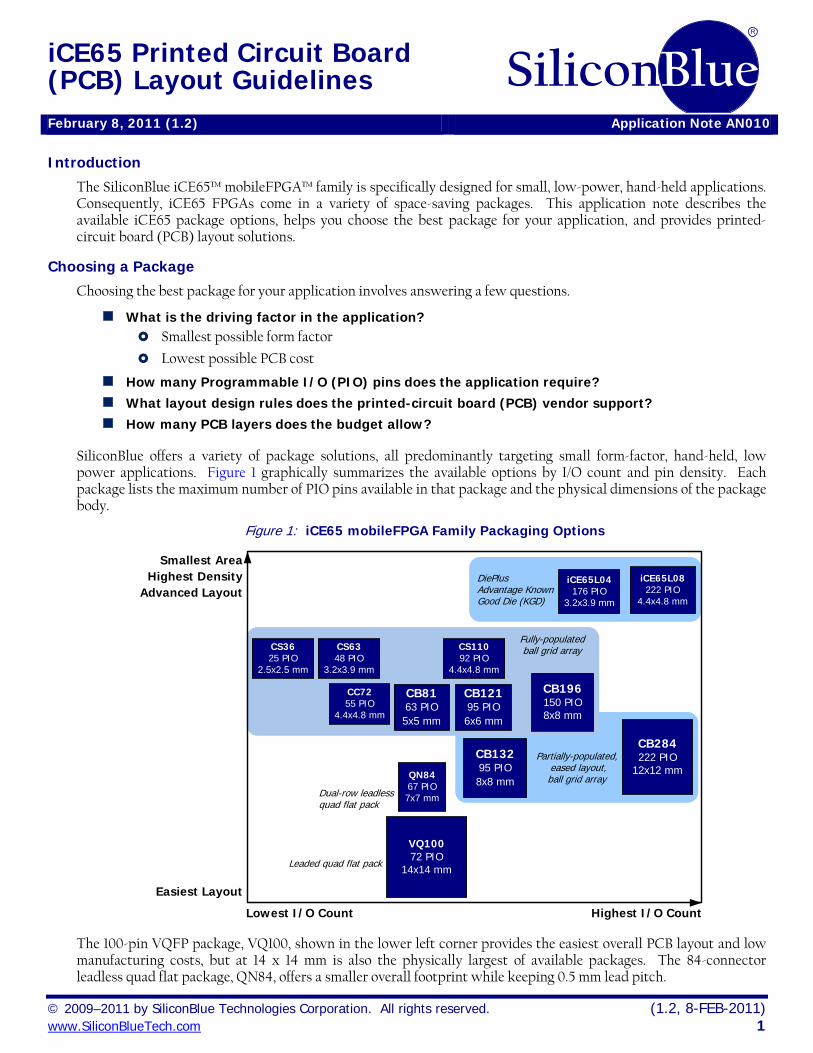
SiliconBlue offers a variety of package solutions, all predominantly targeting small form-factor, hand-held, low power applications. Figure 1 graphically summarizes the available options by I/O count and pin density. Each package lists the maximum number of PIO pins available in that package and the physical dimensions of the package body.
Figure 1: iCE65 mobileFPGA Family Packaging Options
VQ10072 PIO
14x14 mm
Highest I/O Count
Easiest Layout
Advanced LayoutHighest Density
Smallest Area
CS6348 PIO
3.2x3.9 mm
CB196150 PIO8x8 mm
CC7255 PIO
4.4x4.8 mm
CB13295 PIO8x8 mm
CB284222 PIO
12x12 mm
Fully-populatedball grid array
Partially-populated, eased layout,ball grid array
Leaded quad flat pack
iCE65L08222 PIO
4.4x4.8 mm
iCE65L04176 PIO
3.2x3.9 mm
DiePlus Advantage Known Good Die (KGD)
Dual-row leadlessquad flat pack
QN8467 PIO7x7 mm
CS3625 PIO
2.5x2.5 mm
CS11092 PIO
4.4x4.8 mm
CB8163 PIO5x5 mm
CB12195 PIO6x6 mm
Lowest I/O Count
The 100-pin VQFP package, VQ100, shown in the lower left corner provides the easiest overall PCB layout and low manufacturing costs, but at 14 x 14 mm is also the physically largest of available packages. The 84-connector leadless quad flat package, QN84, offers a smaller overall footprint while keeping 0.5 mm lead pitch.
AN010: iCE65 Printed Circuit Board (PCB) Layout Guidelines
(1.2, 8-FEB-2011) SiliconBlue Technologies Corporation 2 www.SiliconBlueTech.com
To provide high package density plus simplified PCB layout, the CB132 and CB284 packages use a partially-populated ball-grid array. Essentially, the balls are arranged in concentric rings with empty rings between ball rings. The empty rings provide space for breaking out signals and for vias between layers. These packages are physically small and provide a large number of PIO pins. The CB284 package, for example, provides up to 222 programmable I/O (PIO) pins.
The fully-populated ball-grid array packages, the CS36, CS63, CC72, CS110, CB121, and the CB196 package are the next step up in I/O pin density but also require tighter PCB layout rules. The CC72, CB121, and CB196 packages use 0.5 mm ball pitch while the CS36, CS63, and CS110 packages use the finer 0.4 mm pitch.
Finally, the ultimate in I/O density are SiliconBlue’s DiePlus™ Advantage Known Good Die (KGD) devices. Using wire-bonding or System-In-Package (SiP) design techniques, the DiePlus Advantage products deliver up to 176 PIO connections in just 12.25 mm2 or 222 PIO connections in 20.98 mm2!
Table 1 lists the maximum number of user-programmable I/O (PIO) pins by package for the iCE65 mobileFPGA family, with additional detail showing the maximum PIO pins by I/O bank. The four SPI I/O pins may be reclaimed as I/O when configuring from SPI Flash or from the internal Nonvolatile Configuration Memory (NVCM).
Table 1: User I/O by Package, by I/O Bank Style Wafer-Level Chip Scale Other Ball Grid Array Code CS36 CS63 CC72 CS110 QN84 VQ100 CB81 CB121 CB132 CB196 CB284
Package Leads 36 63 72 110 84 100 81 121 132 196 284
Package Area (mm)
2.5x 2.5
3.85x 3.18
4.374x 4.79
4.354x 4.770 7x7 14x14 5x5 6x6 8x8 8x8 12x12
Ball Array (balls) 6x6 9x7 9x8 10x11 N/A N/A 9x9 11x11 14x14 14x14 22x22
Ball/Lead Pitch (mm) 0.4 0.4 0.5 0.4 0.5 0.5 0.5 0.5 0.5 0.5 0.5
Maximum user I/O, all banks
25 48 55 92 67 72 63 95 95 150 222
in Bank 0 7 13 11 21 17 19 17 25 26 37 60 in Bank 1 5 11 16 24 17 19 16 21 21 38 55 in Bank 2 2 12 8 19 11 12 8 19 20 35 53 in Bank 3 7 8 16 24 18 18 18 26 24 36 50 SPI bank 4 4 4 4 4 4 4 4 4 4 4
Table 2 lists the maximum available PIO pins by device and by package type. Not all devices are available in all packages. Similarly, smaller iCE65 FPGAs may have unconnected balls when packaged in high pin-count packages. Devices sharing a common package typically have similar footprints although there are minor differences for the CB196 package, as described in the iCE65 data sheet.
Table 2: Maximum User I/O (PIO Pins) by Device and Package
Package Device
iCE65L01 iCE65L04 iCE65P04 iCE65L08 CS36 25 — — — CS63 — 48 — — CC72 — — — 55
CS110 — — — 92 QN84 67 — — — VQ100 72 72 — — CB81 63 — — —
CB121 — — 95 — CB132 93 95 — 95 CB196 — 150 148 150 CB284 — 176 174 222
SiliconBlue
SiliconBlue Technologies Corporation (1.2, 8-FEB-2011) www.SiliconBlueTech.com 3
Layout Examples
SiliconBlue provides pre-designed layout examples for the various package options as listed in Table 3. Some examples, such as the CB284 and CB196, offer different layout options depending on design and cost goals. For instance, one CB284 package layout example includes all the programmable I/O pins but requires finer trace width and pitch. An alternate CB284 layout uses relaxed design rules, with 4 mil spacing, but sacrifices some of the available programmable I/O pins on the iCE65 FPGA.
Table 3: Package Layout Examples
Package Pitch (mm)
SMD/ NSMD
Total Layers
Signal Layers
Pad Size
(mm)
Solder Mask (mm)
Via Drill (mil)
Via Size (mil)
Trace Width (mil)
Trace Space (mil)
CS36 0.4 NSMD 4 2 0.20 0.25 5 10 4 3.5 CS63 0.4 NSMD 6 4 0.20 0.25 5 10 4 3.5 CC72 0.5 NSMD 6 4 0.254 0.4064 6 12 4 4
CS110 0.4 NSMD 6 4 0.20 0.35 5 10 4 4
QN84 0.5 NSMD 1 1 0.4 x 0.22
0.502 x 0.322 N/A N/A 4 3.5
VQ100 0.5 NSMD 4 1 0.30 0.452 5 10 5 5 CB81 0.5 NSMD 4 2 0.20 0.30 6 12 4 3.5
CB121 0.5 NSMD 6 4 0.20 0.30 6 12 4 3.5 CB132 0.5 NSMD 4 2 0.254 0.4064 5 10 3 3 CB132 0.5 NSMD 6 4 0.254 0.4064 6 12 4 4 CB196 0.5 SMD 4 2 0.25 0.25 5 10 3 3 CB196 0.5 NSMD 6 4 0.25 0.4064 5 10 3 3 CB196 0.5 NSMD 8 5 0.254 0.4064 6 12 4 4 CB284 0.5 NSMD 4 2 0.25 0.406 5 10 3 3 CB284 0.5 NSMD 4 2 0.25 0.406 9 18 4 4 CB284 0.5 NSMD 8 5 0.254 0.4064 6 12 4 4
Support Files
The example layout files are available from your local SiliconBlue Technologies’ sales person.
SiliconBlue Sales Representatives www.siliconbluetech.com/sales.aspx
All the layout examples are included in a single ZIP archive file. Each package-specific example is provided in its own directory including Allegro .brd format files that are widely supported by other PCB design software packages. Simply import the .brd files into your favorite PCB design software.
The filename of the .brd file is listed in each of the following package layout sections.
Free Allegro Viewer
If you do not already have a PCB board design software package but would like to view the files, simply download and install the free Allegro viewer software available from Cadence.
Free Cadence Allegro Physical Viewer Downloads www.cadence.com/products/pcb/Pages/downloads.aspx
AN010: iCE65 Printed Circuit Board (PCB) Layout Guidelines
(1.2, 8-FEB-2011) SiliconBlue Technologies Corporation 4 www.SiliconBlueTech.com
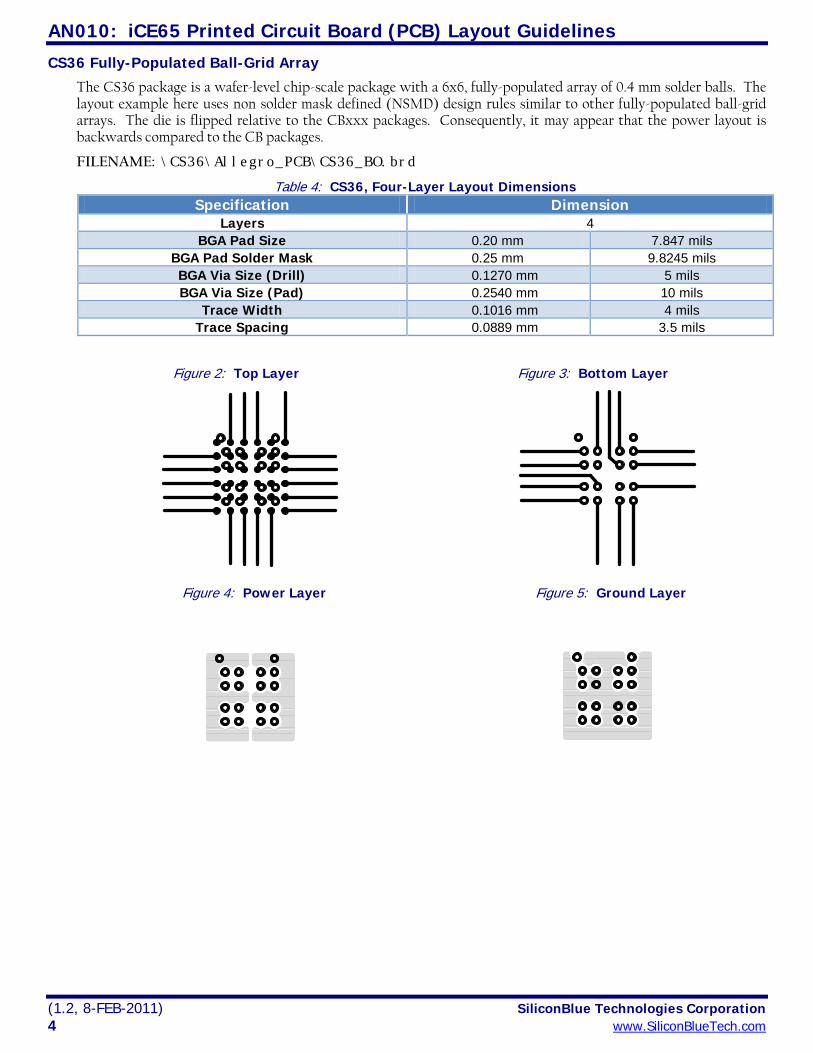
CS36 Fully-Populated Ball-Grid Array
The CS36 package is a wafer-level chip-scale package with a 6x6, fully-populated array of 0.4 mm solder balls. The layout example here uses non solder mask defined (NSMD) design rules similar to other fully-populated ball-grid arrays. The die is flipped relative to the CBxxx packages. Consequently, it may appear that the power layout is backwards compared to the CB packages.
FILENAME: \CS36\Allegro_PCB\CS36_BO.brd
Table 4: CS36, Four-Layer Layout Dimensions Specification Dimension
Layers 4 BGA Pad Size 0.20 mm 7.847 mils
BGA Pad Solder Mask 0.25 mm 9.8245 mils BGA Via Size (Drill) 0.1270 mm 5 mils BGA Via Size (Pad) 0.2540 mm 10 mils
Trace Width 0.1016 mm 4 mils Trace Spacing 0.0889 mm 3.5 mils
Figure 2: Top Layer
Figure 3: Bottom Layer
Figure 4: Power Layer
Figure 5: Ground Layer
SiliconBlue
SiliconBlue Technologies Corporation (1.2, 8-FEB-2011) www.SiliconBlueTech.com 5
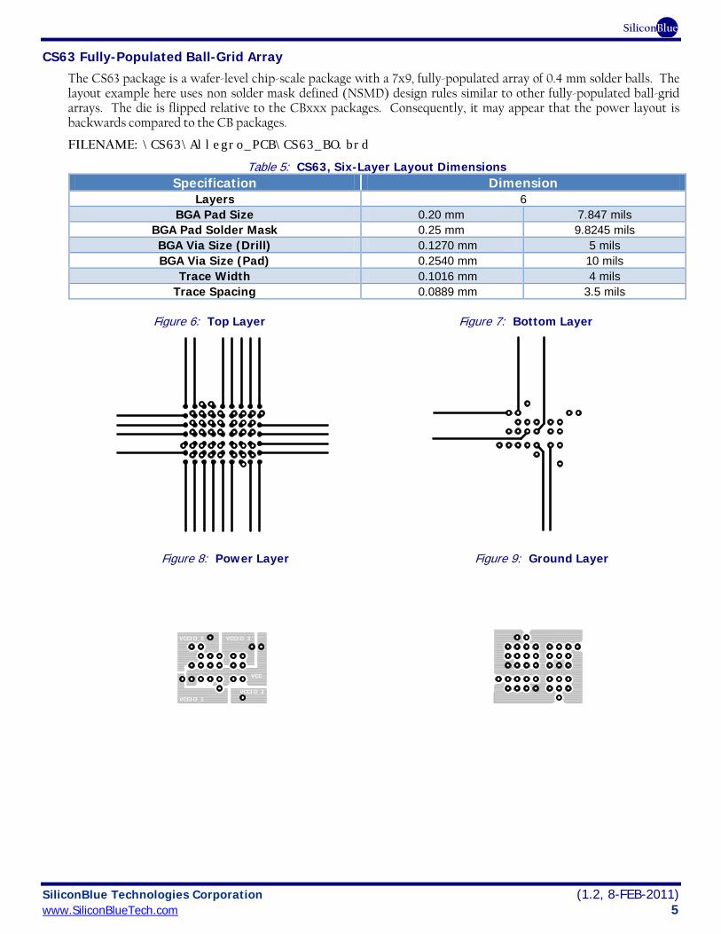
CS63 Fully-Populated Ball-Grid Array
The CS63 package is a wafer-level chip-scale package with a 7x9, fully-populated array of 0.4 mm solder balls. The layout example here uses non solder mask defined (NSMD) design rules similar to other fully-populated ball-grid arrays. The die is flipped relative to the CBxxx packages. Consequently, it may appear that the power layout is backwards compared to the CB packages.
FILENAME: \CS63\Allegro_PCB\CS63_BO.brd
Table 5: CS63, Six-Layer Layout Dimensions Specification Dimension
Layers 6 BGA Pad Size 0.20 mm 7.847 mils
BGA Pad Solder Mask 0.25 mm 9.8245 mils BGA Via Size (Drill) 0.1270 mm 5 mils BGA Via Size (Pad) 0.2540 mm 10 mils
Trace Width 0.1016 mm 4 mils Trace Spacing 0.0889 mm 3.5 mils
Figure 6: Top Layer
Figure 7: Bottom Layer
Figure 8: Power Layer
Figure 9: Ground Layer
VCC
VCCIO_3VCCIO_0
VCCIO_2VCCIO_1
AN010: iCE65 Printed Circuit Board (PCB) Layout Guidelines
(1.2, 8-FEB-2011) SiliconBlue Technologies Corporation 6 www.SiliconBlueTech.com
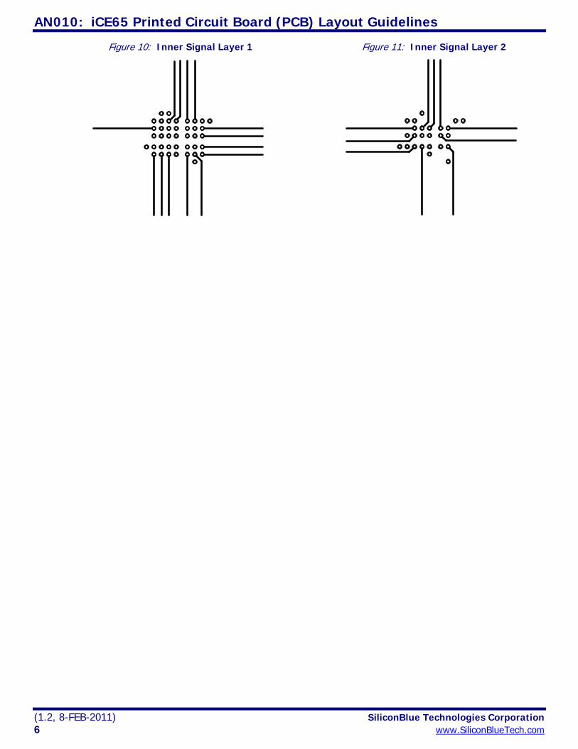
Figure 10: Inner Signal Layer 1
Figure 11: Inner Signal Layer 2
SiliconBlue
SiliconBlue Technologies Corporation (1.2, 8-FEB-2011) www.SiliconBlueTech.com 7
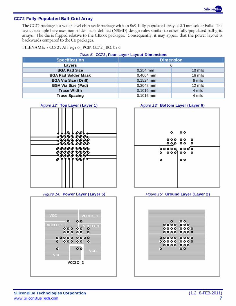
CC72 Fully-Populated Ball-Grid Array
The CC72 package is a wafer-level chip-scale package with an 8x9, fully-populated array of 0.5 mm solder balls. The layout example here uses non solder mask defined (NSMD) design rules similar to other fully-populated ball-grid arrays. The die is flipped relative to the CBxxx packages. Consequently, it may appear that the power layout is backwards compared to the CB packages.
FILENAME: \CC72\Allegro_PCB\CC72_BO.brd
Table 6: CC72, Four-Layer Layout Dimensions Specification Dimension
Layers 6 BGA Pad Size 0.254 mm 10 mils
BGA Pad Solder Mask 0.4064 mm 16 mils BGA Via Size (Drill) 0.1524 mm 6 mils BGA Via Size (Pad) 0.3048 mm 12 mils
Trace Width 0.1016 mm 4 mils Trace Spacing 0.1016 mm 4 mils
Figure 12: Top Layer (Layer 1)
Figure 13: Bottom Layer (Layer 6)
Figure 14: Power Layer (Layer 5)
Figure 15: Ground Layer (Layer 2)
VCC VCCIO_0
VCCIO_3
VCCIO_2
VCCIO_1
VCCVCC
AN010: iCE65 Printed Circuit Board (PCB) Layout Guidelines
(1.2, 8-FEB-2011) SiliconBlue Technologies Corporation 8 www.SiliconBlueTech.com
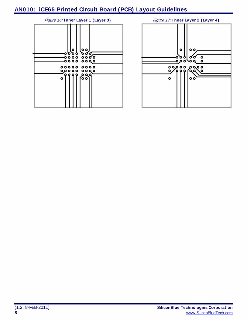
Figure 16: Inner Layer 1 (Layer 3)
Figure 17: Inner Layer 2 (Layer 4)
SiliconBlue
SiliconBlue Technologies Corporation (1.2, 8-FEB-2011) www.SiliconBlueTech.com 9
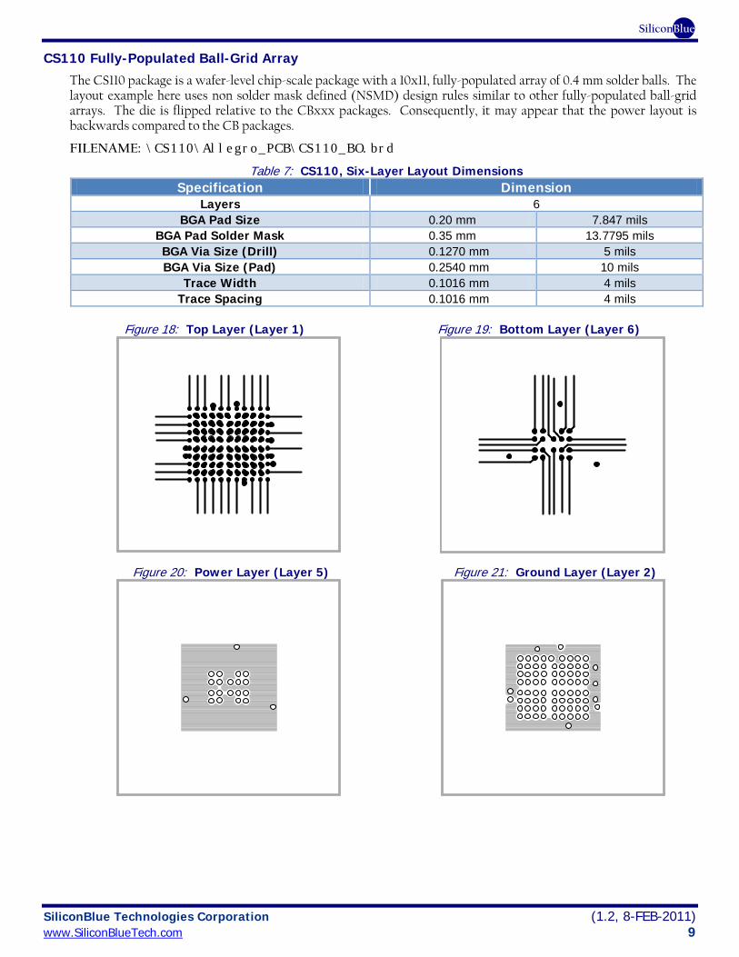
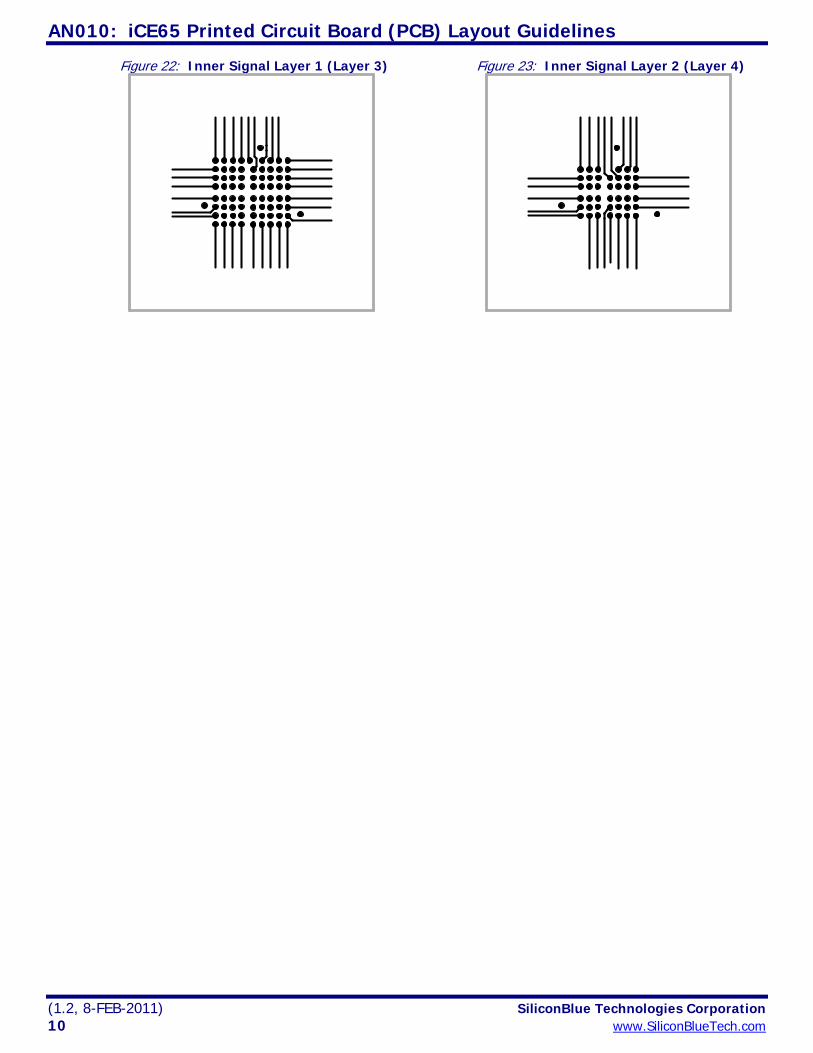
CS110 Fully-Populated Ball-Grid Array
The CS110 package is a wafer-level chip-scale package with a 10x11, fully-populated array of 0.4 mm solder balls. The layout example here uses non solder mask defined (NSMD) design rules similar to other fully-populated ball-grid arrays. The die is flipped relative to the CBxxx packages. Consequently, it may appear that the power layout is backwards compared to the CB packages.
FILENAME: \CS110\Allegro_PCB\CS110_BO.brd
Table 7: CS110, Six-Layer Layout Dimensions Specification Dimension
Layers 6 BGA Pad Size 0.20 mm 7.847 mils
BGA Pad Solder Mask 0.35 mm 13.7795 mils BGA Via Size (Drill) 0.1270 mm 5 mils BGA Via Size (Pad) 0.2540 mm 10 mils
Trace Width 0.1016 mm 4 mils Trace Spacing 0.1016 mm 4 mils
Figure 18: Top Layer (Layer 1)
Figure 19: Bottom Layer (Layer 6)
Figure 20: Power Layer (Layer 5)
Figure 21: Ground Layer (Layer 2)
AN010: iCE65 Printed Circuit Board (PCB) Layout Guidelines
(1.2, 8-FEB-2011) SiliconBlue Technologies Corporation 10 www.SiliconBlueTech.com
Figure 22: Inner Signal Layer 1 (Layer 3)
Figure 23: Inner Signal Layer 2 (Layer 4)
SiliconBlue
SiliconBlue Technologies Corporation (1.2, 8-FEB-2011) www.SiliconBlueTech.com 11
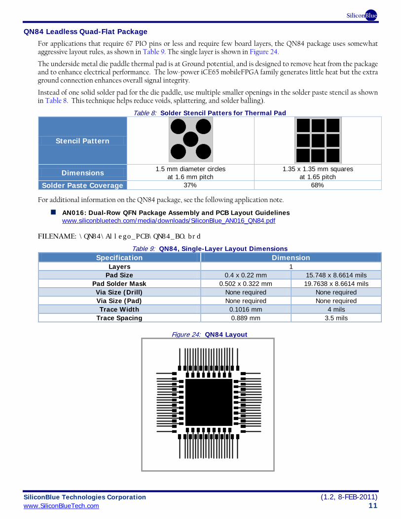
QN84 Leadless Quad-Flat Package
For applications that require 67 PIO pins or less and require few board layers, the QN84 package uses somewhat aggressive layout rules, as shown in Table 9. The single layer is shown in Figure 24.
The underside metal die paddle thermal pad is at Ground potential, and is designed to remove heat from the package and to enhance electrical performance. The low-power iCE65 mobileFPGA family generates little heat but the extra ground connection enhances overall signal integrity.
Instead of one solid solder pad for the die paddle, use multiple smaller openings in the solder paste stencil as shown in Table 8. This technique helps reduce voids, splattering, and solder balling).
Table 8: Solder Stencil Patters for Thermal Pad
Stencil Pattern
Dimensions 1.5 mm diameter circles at 1.6 mm pitch
1.35 x 1.35 mm squares at 1.65 pitch
Solder Paste Coverage 37% 68%
For additional information on the QN84 package, see the following application note.
AN016: Dual-Row QFN Package Assembly and PCB Layout Guidelines www.siliconbluetech.com/media/downloads/SiliconBlue_AN016_QN84.pdf
FILENAME: \QN84\Allego_PCB\QN84_BO.brd
Table 9: QN84, Single-Layer Layout Dimensions Specification Dimension
Layers 1 Pad Size 0.4 x 0.22 mm 15.748 x 8.6614 mils
Pad Solder Mask 0.502 x 0.322 mm 19.7638 x 8.6614 mils Via Size (Drill) None required None required Via Size (Pad) None required None required Trace Width 0.1016 mm 4 mils
Trace Spacing 0.889 mm 3.5 mils
Figure 24: QN84 Layout
AN010: iCE65 Printed Circuit Board (PCB) Layout Guidelines
(1.2, 8-FEB-2011) SiliconBlue Technologies Corporation 12 www.SiliconBlueTech.com
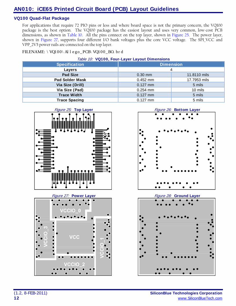
VQ100 Quad-Flat Package
For applications that require 72 PIO pins or less and where board space is not the primary concern, the VQ100 package is the best option. The VQ100 package has the easiest layout and uses very common, low-cost PCB dimensions, as shown in Table 10. All the pins connect on the top layer, shown in Figure 25. The power layer, shown in Figure 27, supports four different I/O bank voltages plus the core VCC voltage. The SPI_VCC and VPP_2V5 power rails are connected on the top layer.
FILENAME: \VQ100\Allego_PCB\VQ100_BO.brd
Table 10: VQ100, Four-Layer Layout Dimensions Specification Dimension
Layers 4 Pad Size 0.30 mm 11.8110 mils
Pad Solder Mask 0.452 mm 17.7953 mils Via Size (Drill) 0.127 mm 5 mils Via Size (Pad) 0.254 mm 10 mils Trace Width 0.127 mm 5 mils
Trace Spacing 0.127 mm 5 mils
Figure 25: Top Layer
Figure 26: Bottom Layer
Figure 27: Power Layer
Figure 28: Ground Layer
SiliconBlue
SiliconBlue Technologies Corporation (1.2, 8-FEB-2011) www.SiliconBlueTech.com 13
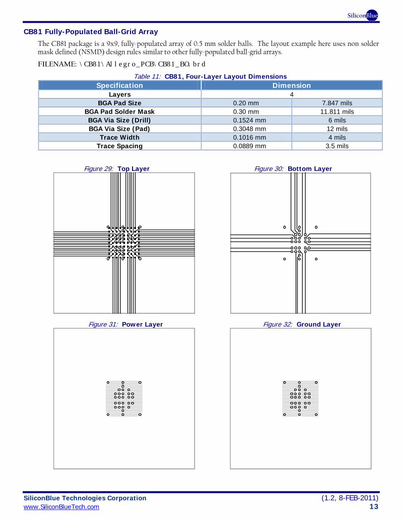
CB81 Fully-Populated Ball-Grid Array
The CB81 package is a 9x9, fully-populated array of 0.5 mm solder balls. The layout example here uses non solder mask defined (NSMD) design rules similar to other fully-populated ball-grid arrays.
FILENAME: \CB81\Allegro_PCB\CB81_BO.brd
Table 11: CB81, Four-Layer Layout Dimensions Specification Dimension
Layers 4 BGA Pad Size 0.20 mm 7.847 mils
BGA Pad Solder Mask 0.30 mm 11.811 mils BGA Via Size (Drill) 0.1524 mm 6 mils BGA Via Size (Pad) 0.3048 mm 12 mils
Trace Width 0.1016 mm 4 mils Trace Spacing 0.0889 mm 3.5 mils
Figure 29: Top Layer
Figure 30: Bottom Layer
Figure 31: Power Layer
Figure 32: Ground Layer
AN010: iCE65 Printed Circuit Board (PCB) Layout Guidelines
(1.2, 8-FEB-2011) SiliconBlue Technologies Corporation 14 www.SiliconBlueTech.com
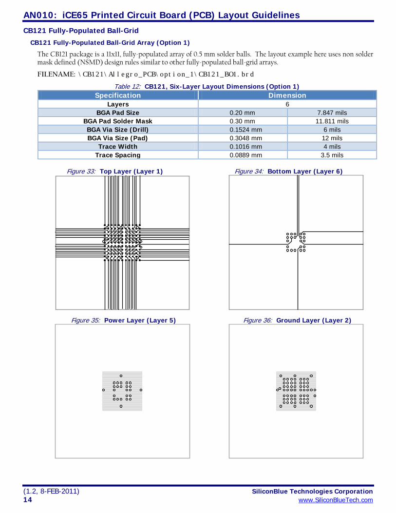
CB121 Fully-Populated Ball-Grid
CB121 Fully-Populated Ball-Grid Array (Option 1)
The CB121 package is a 11x11, fully-populated array of 0.5 mm solder balls. The layout example here uses non solder mask defined (NSMD) design rules similar to other fully-populated ball-grid arrays.
FILENAME: \CB121\Allegro_PCB\option_1\CB121_BO1.brd
Table 12: CB121, Six-Layer Layout Dimensions (Option 1) Specification Dimension
Layers 6 BGA Pad Size 0.20 mm 7.847 mils
BGA Pad Solder Mask 0.30 mm 11.811 mils BGA Via Size (Drill) 0.1524 mm 6 mils BGA Via Size (Pad) 0.3048 mm 12 mils
Trace Width 0.1016 mm 4 mils Trace Spacing 0.0889 mm 3.5 mils
Figure 33: Top Layer (Layer 1)
Figure 34: Bottom Layer (Layer 6)
Figure 35: Power Layer (Layer 5)
Figure 36: Ground Layer (Layer 2)
SiliconBlue
SiliconBlue Technologies Corporation (1.2, 8-FEB-2011) www.SiliconBlueTech.com 15
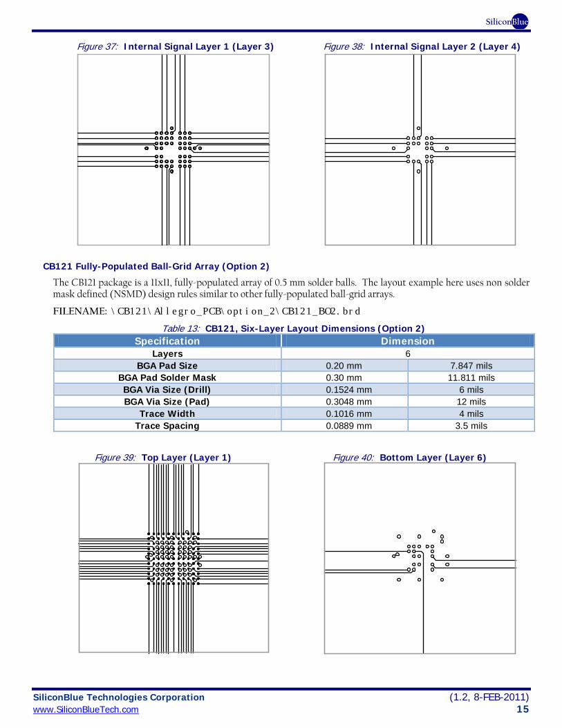
Figure 37: Internal Signal Layer 1 (Layer 3)
Figure 38: Internal Signal Layer 2 (Layer 4)
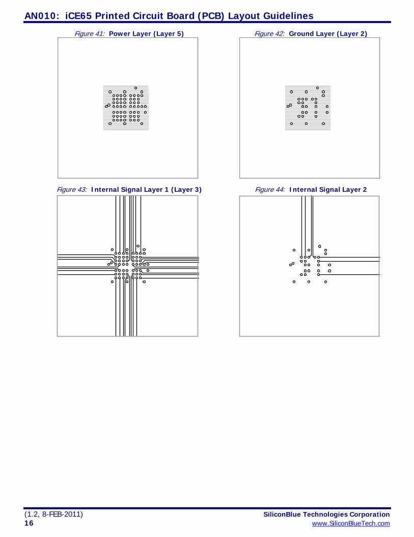
CB121 Fully-Populated Ball-Grid Array (Option 2)
The CB121 package is a 11x11, fully-populated array of 0.5 mm solder balls. The layout example here uses non solder mask defined (NSMD) design rules similar to other fully-populated ball-grid arrays.
FILENAME: \CB121\Allegro_PCB\option_2\CB121_BO2.brd
Table 13: CB121, Six-Layer Layout Dimensions (Option 2) Specification Dimension
Layers 6 BGA Pad Size 0.20 mm 7.847 mils
BGA Pad Solder Mask 0.30 mm 11.811 mils BGA Via Size (Drill) 0.1524 mm 6 mils BGA Via Size (Pad) 0.3048 mm 12 mils
Trace Width 0.1016 mm 4 mils Trace Spacing 0.0889 mm 3.5 mils
Figure 39: Top Layer (Layer 1)
Figure 40: Bottom Layer (Layer 6)
AN010: iCE65 Printed Circuit Board (PCB) Layout Guidelines
(1.2, 8-FEB-2011) SiliconBlue Technologies Corporation 16 www.SiliconBlueTech.com
Figure 41: Power Layer (Layer 5)
Figure 42: Ground Layer (Layer 2)
Figure 43: Internal Signal Layer 1 (Layer 3)
Figure 44: Internal Signal Layer 2
SiliconBlue
SiliconBlue Technologies Corporation (1.2, 8-FEB-2011) www.SiliconBlueTech.com 17
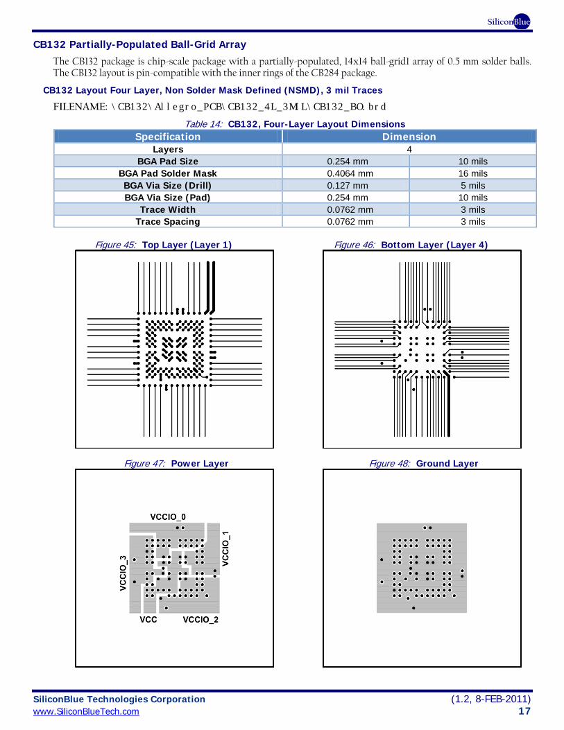
CB132 Partially-Populated Ball-Grid Array
The CB132 package is chip-scale package with a partially-populated, 14x14 ball-grid1 array of 0.5 mm solder balls. The CB132 layout is pin-compatible with the inner rings of the CB284 package.
CB132 Layout Four Layer, Non Solder Mask Defined (NSMD), 3 mil Traces
FILENAME: \CB132\Allegro_PCB\CB132_4L_3MIL\CB132_BO.brd
Table 14: CB132, Four-Layer Layout Dimensions Specification Dimension
Layers 4 BGA Pad Size 0.254 mm 10 mils
BGA Pad Solder Mask 0.4064 mm 16 mils BGA Via Size (Drill) 0.127 mm 5 mils BGA Via Size (Pad) 0.254 mm 10 mils
Trace Width 0.0762 mm 3 mils Trace Spacing 0.0762 mm 3 mils
Figure 45: Top Layer (Layer 1)
Figure 46: Bottom Layer (Layer 4)
Figure 47: Power Layer
Figure 48: Ground Layer
AN010: iCE65 Printed Circuit Board (PCB) Layout Guidelines
(1.2, 8-FEB-2011) SiliconBlue Technologies Corporation 18 www.SiliconBlueTech.com
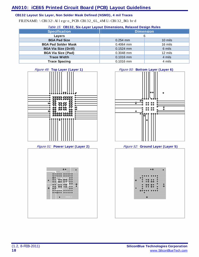
CB132 Layout Six Layer, Non Solder Mask Defined (NSMD), 4 mil Traces
FILENAME: \CB132\Allegro_PCB\CB132_6L_4MIL\CB132_BO.brd
Table 15: CB132, Six-Layer Layout Dimensions, Relaxed Design Rules Specification Dimension
Layers 6 BGA Pad Size 0.254 mm 10 mils
BGA Pad Solder Mask 0.4064 mm 16 mils BGA Via Size (Drill) 0.1524 mm 6 mils BGA Via Size (Pad) 0.3048 mm 12 mils
Trace Width 0.1016 mm 4 mils Trace Spacing 0.1016 mm 4 mils
Figure 49: Top Layer (Layer 1)
Figure 50: Bottom Layer (Layer 6)
Figure 51: Power Layer (Layer 2)
Figure 52: Ground Layer (Layer 5)
VCC
VCCIO_0 VCCIO_1
VCCIO_2
VCCIO_3
SiliconBlue
SiliconBlue Technologies Corporation (1.2, 8-FEB-2011) www.SiliconBlueTech.com 19
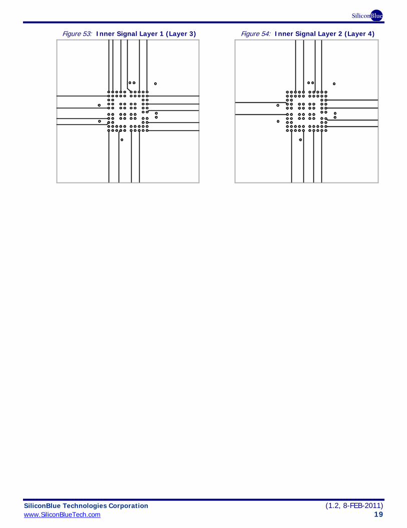
Figure 53: Inner Signal Layer 1 (Layer 3)
Figure 54: Inner Signal Layer 2 (Layer 4)
AN010: iCE65 Printed Circuit Board (PCB) Layout Guidelines
(1.2, 8-FEB-2011) SiliconBlue Technologies Corporation 20 www.SiliconBlueTech.com
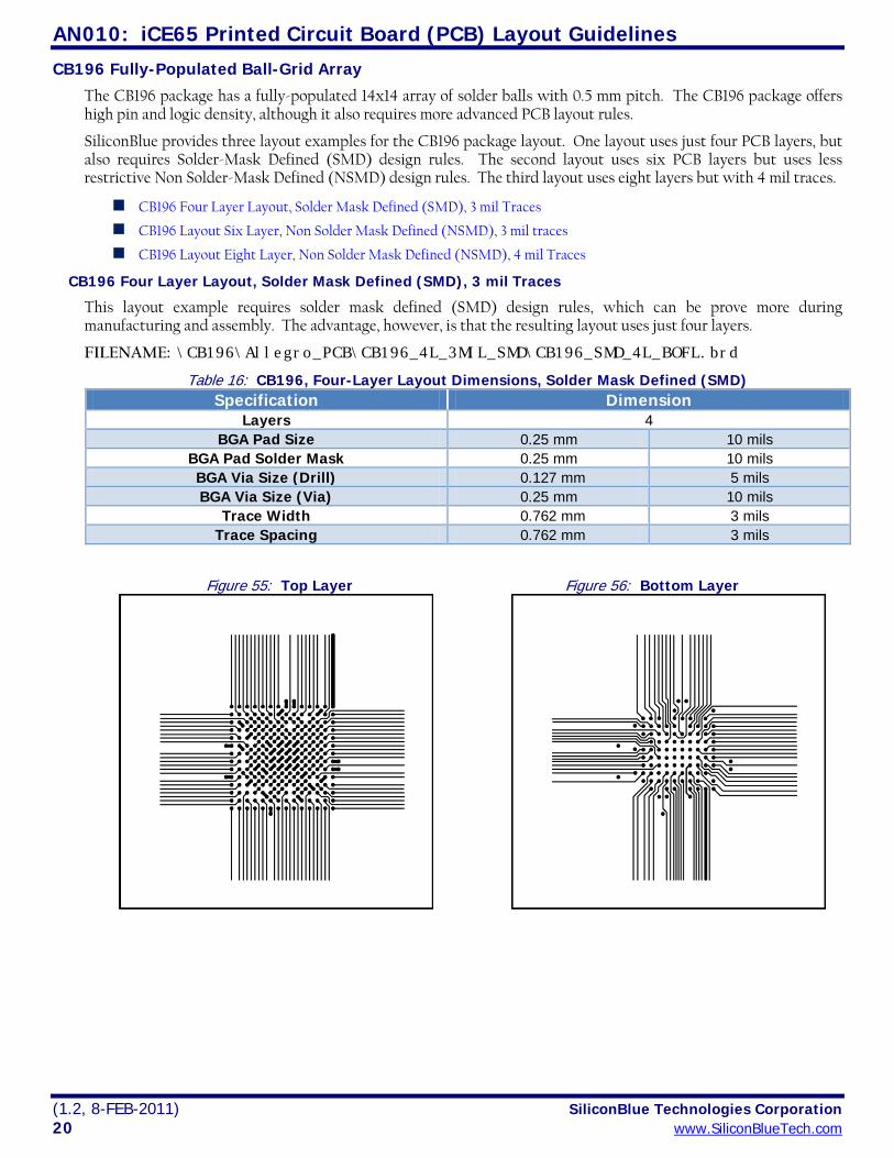
CB196 Fully-Populated Ball-Grid Array
The CB196 package has a fully-populated 14x14 array of solder balls with 0.5 mm pitch. The CB196 package offers high pin and logic density, although it also requires more advanced PCB layout rules.
SiliconBlue provides three layout examples for the CB196 package layout. One layout uses just four PCB layers, but also requires Solder-Mask Defined (SMD) design rules. The second layout uses six PCB layers but uses less restrictive Non Solder-Mask Defined (NSMD) design rules. The third layout uses eight layers but with 4 mil traces.
CB196 Four Layer Layout, Solder Mask Defined (SMD), 3 mil Traces
CB196 Layout Six Layer, Non Solder Mask Defined (NSMD), 3 mil traces
CB196 Layout Eight Layer, Non Solder Mask Defined (NSMD), 4 mil Traces
CB196 Four Layer Layout, Solder Mask Defined (SMD), 3 mil Traces
This layout example requires solder mask defined (SMD) design rules, which can be prove more during manufacturing and assembly. The advantage, however, is that the resulting layout uses just four layers.
FILENAME: \CB196\Allegro_PCB\CB196_4L_3MIL_SMD\CB196_SMD_4L_BOFL.brd
Table 16: CB196, Four-Layer Layout Dimensions, Solder Mask Defined (SMD) Specification Dimension
Layers 4 BGA Pad Size 0.25 mm 10 mils
BGA Pad Solder Mask 0.25 mm 10 mils BGA Via Size (Drill) 0.127 mm 5 mils BGA Via Size (Via) 0.25 mm 10 mils
Trace Width 0.762 mm 3 mils Trace Spacing 0.762 mm 3 mils
Figure 55: Top Layer
Figure 56: Bottom Layer
SiliconBlue
SiliconBlue Technologies Corporation (1.2, 8-FEB-2011) www.SiliconBlueTech.com 21
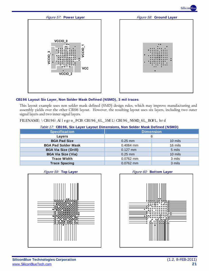
Figure 57: Power Layer
Figure 58: Ground Layer
CB196 Layout Six Layer, Non Solder Mask Defined (NSMD), 3 mil traces
This layout example uses non solder mask defined (SMD) design rules, which may improve manufacturing and assembly yields over the other CB196 layout. However, the resulting layout uses six layers, including two outer signal layers and two inner signal layers.
FILENAME: \CB196\Allegro_PCB\CB196_6L_3MIL\CB196_NSMD_6L_BOFL.brd
Table 17: CB196, Six-Layer Layout Dimensions, Non Solder Mask Defined (NSMD) Specification Dimension
Layers 6 BGA Pad Size 0.25 mm 10 mils
BGA Pad Solder Mask 0.4064 mm 16 mils BGA Via Size (Drill) 0.127 mm 5 mils BGA Via Size (Via) 0.25 mm 10 mils
Trace Width 0.0762 mm 3 mils Trace Spacing 0.0762 mm 3 mils
Figure 59: Top Layer
Figure 60: Bottom Layer
AN010: iCE65 Printed Circuit Board (PCB) Layout Guidelines
(1.2, 8-FEB-2011) SiliconBlue Technologies Corporation 22 www.SiliconBlueTech.com
Figure 61: Power Layer
Figure 62: Ground Layer
Figure 63: Inner Signal Layer 1
Figure 64: Inner Signal Layer 2
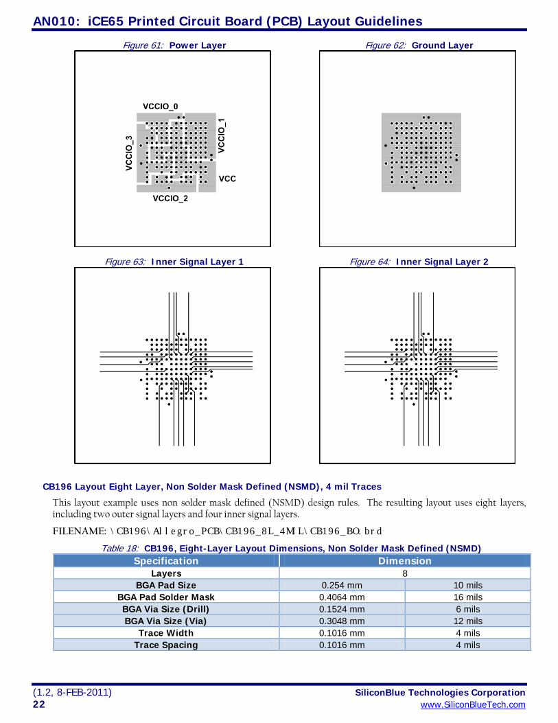
CB196 Layout Eight Layer, Non Solder Mask Defined (NSMD), 4 mil Traces
This layout example uses non solder mask defined (NSMD) design rules. The resulting layout uses eight layers, including two outer signal layers and four inner signal layers.
FILENAME: \CB196\Allegro_PCB\CB196_8L_4MIL\CB196_BO.brd
Table 18: CB196, Eight-Layer Layout Dimensions, Non Solder Mask Defined (NSMD) Specification Dimension
Layers 8 BGA Pad Size 0.254 mm 10 mils
BGA Pad Solder Mask 0.4064 mm 16 mils BGA Via Size (Drill) 0.1524 mm 6 mils BGA Via Size (Via) 0.3048 mm 12 mils
Trace Width 0.1016 mm 4 mils Trace Spacing 0.1016 mm 4 mils
SiliconBlue
SiliconBlue Technologies Corporation (1.2, 8-FEB-2011) www.SiliconBlueTech.com 23
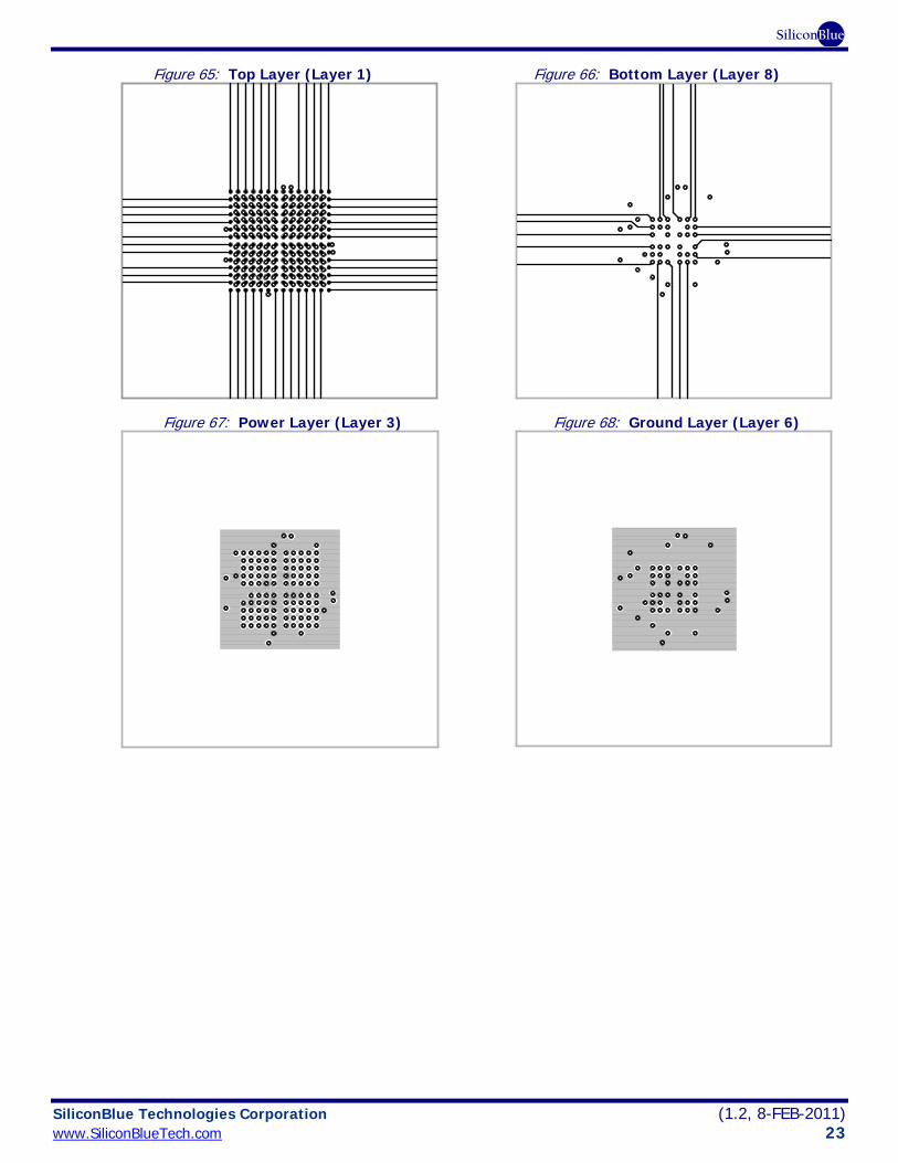
Figure 65: Top Layer (Layer 1)
Figure 66: Bottom Layer (Layer 8)
Figure 67: Power Layer (Layer 3)
Figure 68: Ground Layer (Layer 6)
AN010: iCE65 Printed Circuit Board (PCB) Layout Guidelines
(1.2, 8-FEB-2011) SiliconBlue Technologies Corporation 24 www.SiliconBlueTech.com
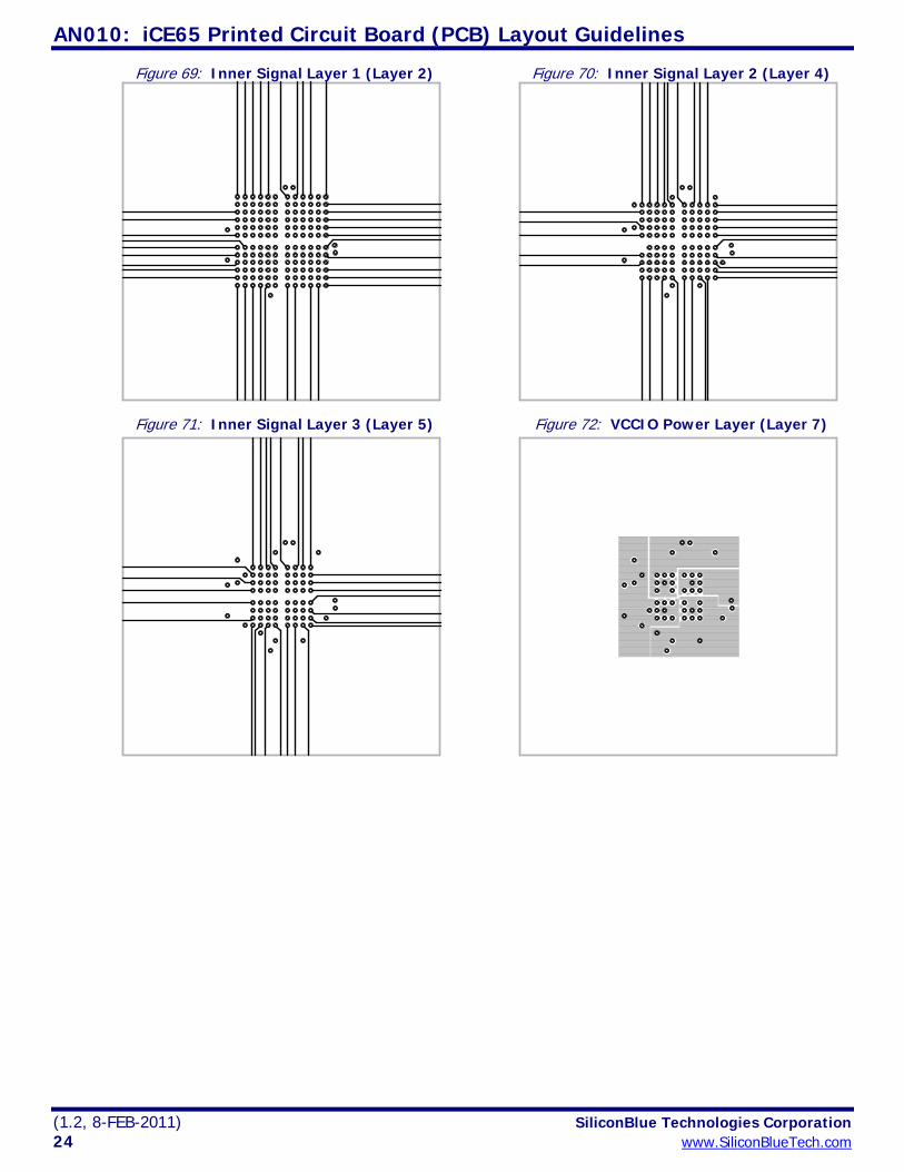
Figure 69: Inner Signal Layer 1 (Layer 2)
Figure 70: Inner Signal Layer 2 (Layer 4)
Figure 71: Inner Signal Layer 3 (Layer 5)
Figure 72: VCCIO Power Layer (Layer 7)
SiliconBlue
SiliconBlue Technologies Corporation (1.2, 8-FEB-2011) www.SiliconBlueTech.com 25
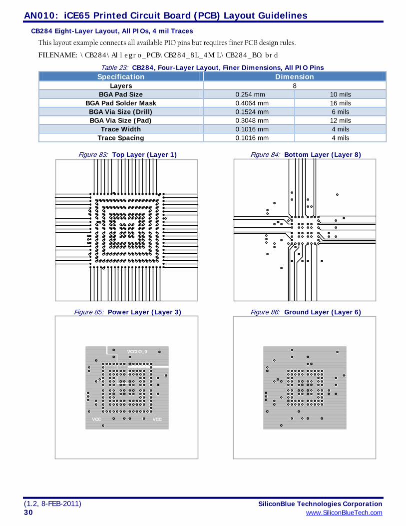
CB284 Partially-Populated Ball Grid Array
Although the CB284 package uses 0.5 mm ball spacing, its partially-populated ball grid simplifies board layout. This application note provides three different design solutions for the CB284 package.
SiliconBlue provides three layout examples for the CB284 package layout. One layout uses just four PCB layers, but requires 3 mil traces. The second layout also uses four layers with 4 mil traces, but does not provide all I/O pins. The third layout uses eight layers but with 4 mil traces.
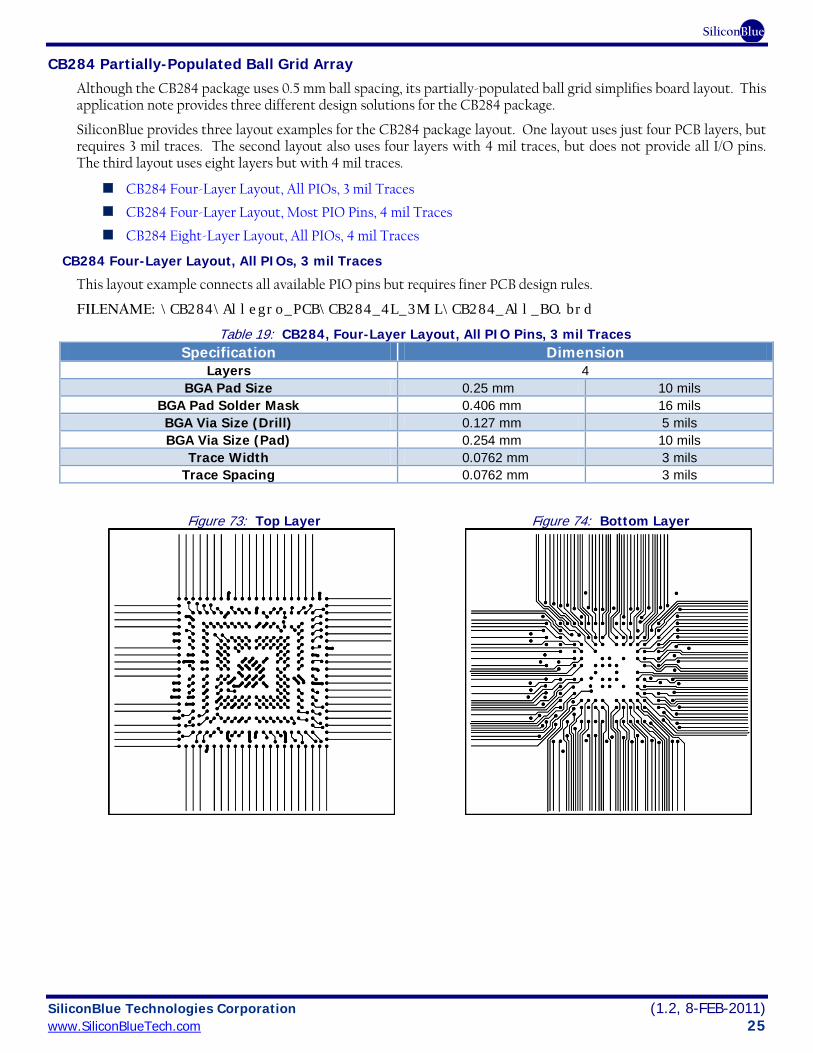
CB284 Four-Layer Layout, All PIOs, 3 mil Traces
CB284 Four-Layer Layout, Most PIO Pins, 4 mil Traces
CB284 Eight-Layer Layout, All PIOs, 4 mil Traces
CB284 Four-Layer Layout, All PIOs, 3 mil Traces
This layout example connects all available PIO pins but requires finer PCB design rules.
FILENAME: \CB284\Allegro_PCB\CB284_4L_3MIL\CB284_All_BO.brd
Table 19: CB284, Four-Layer Layout, All PIO Pins, 3 mil Traces Specification Dimension
Layers 4 BGA Pad Size 0.25 mm 10 mils
BGA Pad Solder Mask 0.406 mm 16 mils BGA Via Size (Drill) 0.127 mm 5 mils BGA Via Size (Pad) 0.254 mm 10 mils
Trace Width 0.0762 mm 3 mils Trace Spacing 0.0762 mm 3 mils
Figure 73: Top Layer
Figure 74: Bottom Layer
AN010: iCE65 Printed Circuit Board (PCB) Layout Guidelines
(1.2, 8-FEB-2011) SiliconBlue Technologies Corporation 26 www.SiliconBlueTech.com
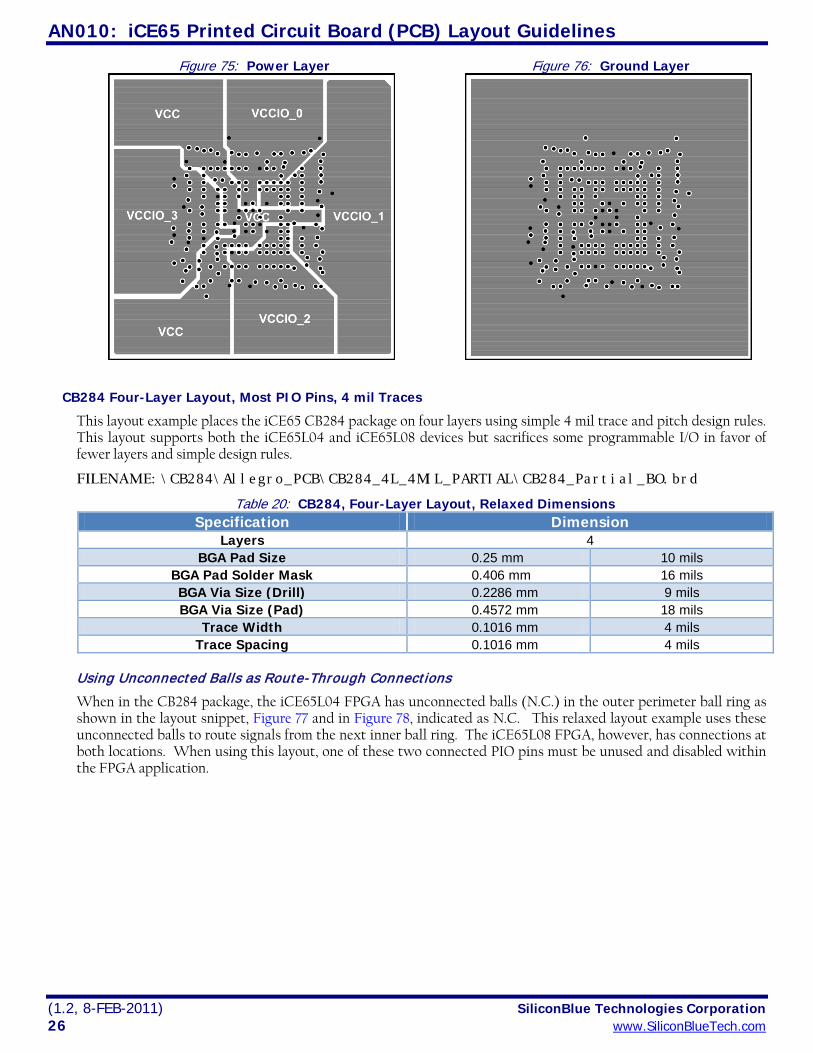
Figure 75: Power Layer
Figure 76: Ground Layer
CB284 Four-Layer Layout, Most PIO Pins, 4 mil Traces
This layout example places the iCE65 CB284 package on four layers using simple 4 mil trace and pitch design rules. This layout supports both the iCE65L04 and iCE65L08 devices but sacrifices some programmable I/O in favor of fewer layers and simple design rules.
FILENAME: \CB284\Allegro_PCB\CB284_4L_4MIL_PARTIAL\CB284_Partial_BO.brd
Table 20: CB284, Four-Layer Layout, Relaxed Dimensions Specification Dimension
Layers 4 BGA Pad Size 0.25 mm 10 mils
BGA Pad Solder Mask 0.406 mm 16 mils BGA Via Size (Drill) 0.2286 mm 9 mils BGA Via Size (Pad) 0.4572 mm 18 mils
Trace Width 0.1016 mm 4 mils Trace Spacing 0.1016 mm 4 mils
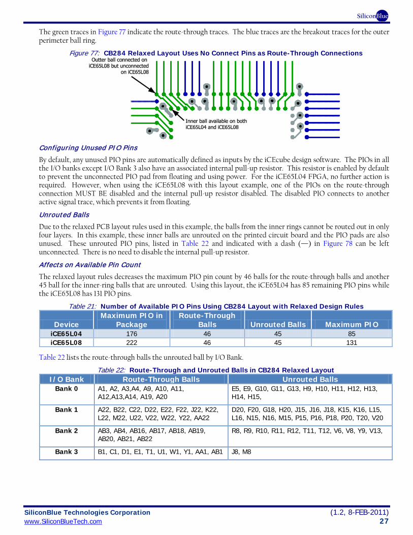
Using Unconnected Balls as Route-Through Connections
When in the CB284 package, the iCE65L04 FPGA has unconnected balls (N.C.) in the outer perimeter ball ring as shown in the layout snippet, Figure 77 and in Figure 78, indicated as N.C. This relaxed layout example uses these unconnected balls to route signals from the next inner ball ring. The iCE65L08 FPGA, however, has connections at both locations. When using this layout, one of these two connected PIO pins must be unused and disabled within the FPGA application.
SiliconBlue
SiliconBlue Technologies Corporation (1.2, 8-FEB-2011) www.SiliconBlueTech.com 27
The green traces in Figure 77 indicate the route-through traces. The blue traces are the breakout traces for the outer perimeter ball ring.
Figure 77: CB284 Relaxed Layout Uses No Connect Pins as Route-Through Connections
Configuring Unused PIO P ins
By default, any unused PIO pins are automatically defined as inputs by the iCEcube design software. The PIOs in all the I/O banks except I/O Bank 3 also have an associated internal pull-up resistor. This resistor is enabled by default to prevent the unconnected PIO pad from floating and using power. For the iCE65L04 FPGA, no further action is required. However, when using the iCE65L08 with this layout example, one of the PIOs on the route-through connection MUST BE disabled and the internal pull-up resistor disabled. The disabled PIO connects to another active signal trace, which prevents it from floating.
Unrouted Balls
Due to the relaxed PCB layout rules used in this example, the balls from the inner rings cannot be routed out in only four layers. In this example, these inner balls are unrouted on the printed circuit board and the PIO pads are also unused. These unrouted PIO pins, listed in Table 22 and indicated with a dash (—) in Figure 78 can be left unconnected. There is no need to disable the internal pull-up resistor.
Affects on Available P in Count
The relaxed layout rules decreases the maximum PIO pin count by 46 balls for the route-through balls and another 45 ball for the inner-ring balls that are unrouted. Using this layout, the iCE65L04 has 85 remaining PIO pins while the iCE65L08 has 131 PIO pins.
Table 21: Number of Available PIO Pins Using CB284 Layout with Relaxed Design Rules
Device Maximum PIO in
Package Route-Through
Balls Unrouted Balls Maximum PIO iCE65L04 176 46 45 85 iCE65L08 222 46 45 131
Table 22 lists the route-through balls the unrouted ball by I/O Bank.
Table 22: Route-Through and Unrouted Balls in CB284 Relaxed Layout I/O Bank Route-Through Balls Unrouted Balls
Bank 0 A1, A2, A3,A4, A9, A10, A11, A12,A13,A14, A19, A20
E5, E9, G10, G11, G13, H9, H10, H11, H12, H13, H14, H15,
Bank 1 A22, B22, C22, D22, E22, F22, J22, K22, L22, M22, U22, V22, W22, Y22, AA22
D20, F20, G18, H20, J15, J16, J18, K15, K16, L15, L16, N15, N16, M15, P15, P16, P18, P20, T20, V20
Bank 2 AB3, AB4, AB16, AB17, AB18, AB19, AB20, AB21, AB22
R8, R9, R10, R11, R12, T11, T12, V6, V8, Y9, V13,
Bank 3 B1, C1, D1, E1, T1, U1, W1, Y1, AA1, AB1 J8, M8
AN010: iCE65 Printed Circuit Board (PCB) Layout Guidelines
(1.2, 8-FEB-2011) SiliconBlue Technologies Corporation 28 www.SiliconBlueTech.com
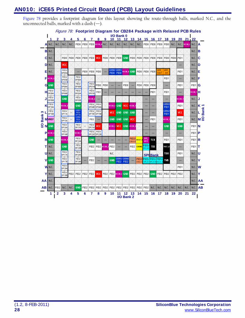
Figure 78 provides a footprint diagram for this layout showing the route-through balls, marked N.C., and the unconnected balls, marked with a dash (—).
Figure 78: Footprint Diagram for CB284 Package with Relaxed PCB Rules
1 2 3 4 5 6 7 8 9 10 11 12 13 14 15 16 17 18 19 20 21 22A
B
C
D
E
F
G
H
J
K
L
M
N
P
R
T
W
Y
AA
AB
1 2 3 4 5 6 7 8 9 10 11 12 13 14 15 16 17 18 19 20 21 22
A
B
C
D
E
F
G
H
J
K
L
M
N
P
R
T
W
Y
AA
AB
U
V
U
V
N.C. N.C. N.C. PIO0 PIO0 PIO0 VCCIO_0VCCIO_0N.C. N.C. N.C. N.C. N.C. N.C. PIO0N.C. PIO0 PIO0 PIO0 N.C. N.C. N.C.
VCCIO_0
VCC
VCC
GND
GND VPP_FAST
VPP_2V5
PIO0 PIO0 PIO0 PIO0 PIO0 PIO0 PIO0 PIO0 PIO0 PIO0 PIO0 PIO0 PIO0 PIO0 PIO0
— PIO0 PIO0 PIO0 — GBIN0/PIO0
GBIN1/PIO0 PIO0 PIO0 PIO0
PIO0 PIO0
—
—
—
—
—
PIO0
—
—
—
PIO0
—
PIO0
—
PIO0
VCCIO_0 GND VCC VCCIO_1
GND GND GND
GND GND GND
GND
VCC
VCC
VCC
VCCIO_3 VCCIO_2
VCCIO_3
GND
GND
VCCIO_3 GND
VCCIO_3
VCCGND
VCCIO_3
GND VCCIO_3
GND
VCCIO_3
GND
GND
VCC VCCIO_2 GND
GND
VCCIO_2
GND
GND
SPI_VCC
GND GND
VCCIO_1
VCC
VCCIO_1
VCCIO_1
TCK
TDI
TDO
TMS
TRST_B
CRESET_B
CDONE
N.C.
N.C.
N.C.
N.C. PIO3/DP05A
PIO3/DP05B
PIO3/DP06A
PIO3/DP06B
PIO3/DP00A
PIO3/DP00B
PIO3/DP03A
PIO3/DP03B
PIO3/DP01A
PIO3/DP01B PIO3
—
PIO3/DP09A
PIO3/DP09B
PIO3/DP10A
PIO3/DP10B
VREF
PIO3/DP04A
PIO3/DP04B
PIO3/DP19B
PIO3/DP19A
—PIO3
GBIN7/PIO3/
DP11B
PIO3/DP11A
GBIN6/PIO3/
DP15A
PIO3/DP15A
PIO3/DP21A
PIO3/DP21B
PIO3/DP22B
PIO3/DP22A
PIO3/DP16A
PIO3/DP16B
N.C.
N.C.
N.C.
N.C.
N.C.
N.C.
PIO3/DP17A
PIO3/DP17B
PIO3/DP18A
PIO3/DP18B
PIO3/DP23A
PIO3/DP23B
PIO3/DP24A
PIO3/DP24B
N.C.
N.C.
N.C.
N.C.
N.C.
PIO1
PIO1
—
PIO1
—
PIO1
—
PIO1
—
PIO1
—
PIO1
—
—
—
—
——
GBIN3/PIO1
GBIN2/PIO1
PIO1
N.C.
N.C.
N.C.
N.C.PIO1PIO1—
—— PIO1
— — — — PIO1
PIO1 PIO1 PIO1
PIOS/SPI_SO
— PIO1
PIO1
—
PIO1
N.C.
N.C.
N.C.
N.C.
N.C.
PIO2 PIO2 PIO2 PIO2PIO2 PIO2 PIO2
PIOS/SPI_SI
PIOS/SPI_SCK
PIOS/SPI_SS_B
PIO2 PIO2 PIO2 PIO2 PIO2 PIO2 N.C. N.C. N.C. N.C. N.C. N.C. N.C.
PIO2/CBSEL0
PIO2
—
—
—
—
—
PIO2
——
PIO2PIO2
— PIO2 — — GBIN5/PIO2
GBIN4/PIO2 — PIO2/
CBSEL1
PIO2 PIO2PIO2 PIO2 PIO2 PIO2
PIO2 N.C. N.C. PIO2 PIO2 PIO2 PIO2
I/O Bank 0
I/O Bank 2
I/O B
ank
1
I/O B
ank
3
SPI BankN.C.
SiliconBlue
SiliconBlue Technologies Corporation (1.2, 8-FEB-2011) www.SiliconBlueTech.com 29
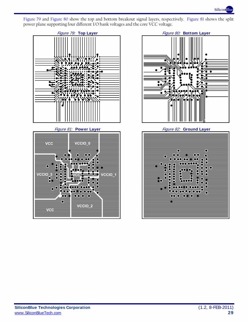
Figure 79 and Figure 80 show the top and bottom breakout signal layers, respectively. Figure 81 shows the split power plane supporting four different I/O bank voltages and the core VCC voltage.
Figure 79: Top Layer
Figure 80: Bottom Layer
Figure 81: Power Layer
Figure 82: Ground Layer
AN010: iCE65 Printed Circuit Board (PCB) Layout Guidelines
(1.2, 8-FEB-2011) SiliconBlue Technologies Corporation 30 www.SiliconBlueTech.com
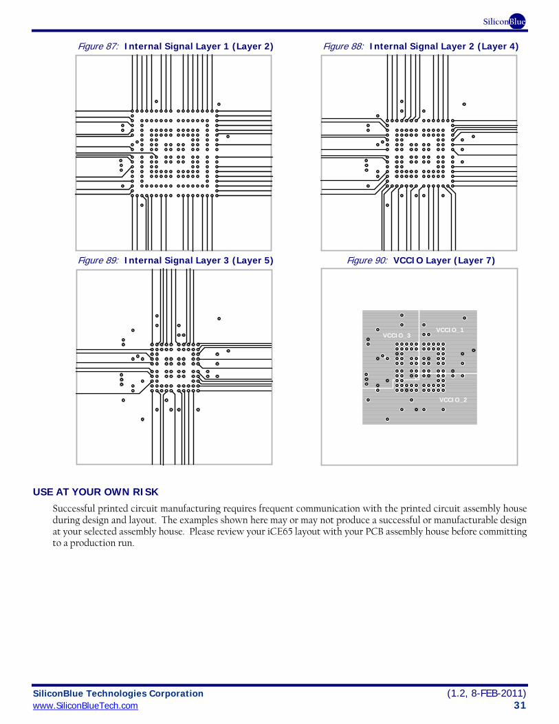
CB284 Eight-Layer Layout, All PIOs, 4 mil Traces
This layout example connects all available PIO pins but requires finer PCB design rules.
FILENAME: \CB284\Allegro_PCB\CB284_8L_4MIL\CB284_BO.brd
Table 23: CB284, Four-Layer Layout, Finer Dimensions, All PIO Pins Specification Dimension
Layers 8 BGA Pad Size 0.254 mm 10 mils
BGA Pad Solder Mask 0.4064 mm 16 mils BGA Via Size (Drill) 0.1524 mm 6 mils BGA Via Size (Pad) 0.3048 mm 12 mils
Trace Width 0.1016 mm 4 mils Trace Spacing 0.1016 mm 4 mils
Figure 83: Top Layer (Layer 1)
Figure 84: Bottom Layer (Layer 8)
Figure 85: Power Layer (Layer 3)
Figure 86: Ground Layer (Layer 6)
VCCIO_0
VCCVCC
SiliconBlue
SiliconBlue Technologies Corporation (1.2, 8-FEB-2011) www.SiliconBlueTech.com 31
Figure 87: Internal Signal Layer 1 (Layer 2)
Figure 88: Internal Signal Layer 2 (Layer 4)
Figure 89: Internal Signal Layer 3 (Layer 5)
Figure 90: VCCIO Layer (Layer 7)
USE AT YOUR OWN RISK
Successful printed circuit manufacturing requires frequent communication with the printed circuit assembly house during design and layout. The examples shown here may or may not produce a successful or manufacturable design at your selected assembly house. Please review your iCE65 layout with your PCB assembly house before committing to a production run.
VCCIO_3VCCIO_1
VCCIO_2
AN010: iCE65 Printed Circuit Board (PCB) Layout Guidelines
(1.2, 8-FEB-2011) SiliconBlue Technologies Corporation 32 www.SiliconBlueTech.com
Revision History
Version Date Description 1.2 8-FEB-2011 Added layout information for the CS36, CS110, CB81, and CB121 packages. Added
improved layout for the CS63 package. Added new 4 mil layout options for the CB132, CB196 and CB284 packages.
1.1 9-AUG-2010 Added QN84 package information for iCE65L01. 1.0.1 30-JUL-2009 Minor updates. 1.0 20-JUL-2009 Initial release.
Disclaimer SILICONBLUE TECHNOLOGIES PROVIDES THIS APPLICATION NOTE TO YOU “AS-IS”. ALL WARRANTIES, REPRESENTATIONS, OR GUARANTEES OF ANY KIND (WHETHER EXPRESS, IMPLIED, OR STATUTORY) INCLUDING, WITHOUT LIMITATION, WARRANTIES OF MERCHANTABILITY, NON-INFRINGEMENT, OR FITNESS FOR A PARTICULAR PURPOSE, ARE SPECIFICALLY DISCLAIMED.
LIMITATION OF LIABILITY: SUBJECT TO APPLICABLE LAWS: (1) IN NO EVENT WILL SILICONBLUE TECHNOLOGIES OR ITS LICENSORS BE LIABLE FOR ANY LOSS OF DATA, LOST PROFITS, COST OF PROCUREMENT OF SUBSTITUTE GOODS OR SERVICES, OR FOR ANY SPECIAL, INCIDENTAL, CONSEQUENTIAL OR INDIRECT DAMAGES ARISING FROM THE USE OR IMPLEMENTATION OF THE APPLICATION NOTE, IN WHOLE OR IN PART, HOWEVER CAUSED AND UNDER ANY THEORY OF LIABILITY; (2) THIS LIMITATION WILL APPLY EVEN IF SILICONBLUE TECHNOLOGIES HAS BEEN ADVISED OF THE POSSIBILITY OF SUCH DAMAGES; (3) THIS LIMITATION SHALL APPLY NOTWITHSTANDING THE FAILURE OF THE ESSENTIAL PURPOSE OF ANY LIMITED REMEDIES HEREIN.
Copyright © 2009 – 2011 by SiliconBlue Technologies LTD. All rights reserved. SiliconBlue is a registered trademark of SiliconBlue Technologies LTD in the United States. Specific device designations, and all other words and logos that are identified as trademarks are, unless noted otherwise, the trademarks of SiliconBlue Technologies LTD. All other product or service names are the property of their respective holders. SiliconBlue products are protected under numerous United States and foreign patents and pending applications, maskwork rights, and copyrights. SiliconBlue warrants performance of its semiconductor products to current specifications in accordance with SiliconBlue's standard warranty, but reserves the right to make changes to any products and services at any time without notice. SiliconBlue assumes no responsibility or liability arising out of the application or use of any information, product, or service described herein except as expressly agreed to in writing by SiliconBlue Technologies LTD. SiliconBlue customers are advised to obtain the latest version of device specifications before relying on any published information and before placing orders for products or services.
SiliconBlueR
SiliconBlue Technologies Corporation
3255 Scott Blvd. Building 7, Suite 101 Santa Clara, California 95054 United States of America
Tel: +1 408-727-6101 Fax: +1 408-727-6085
www.SiliconBlueTech.com Doc umentation services by Prevailing Technol ogy, Inc . (www.prevaili ng-tec hnol ogy .com)