Embed Size (px)
Citation preview

ON-CHIP CURRENT SENSING TECHNIQUE FOR CMOS MONOLITHIC SWITCH-MODE POWER CONVERTERS
Manmeet Singh

2
Presentation Outlines
The Need for Current Sensing Current Sensing Techniques – Overview The Chosen Technique – SENSEFET
Article Overview Measurements Results Circuit Efficiency and Performance Conclusions & Summary
3
The Need for Current-Sensing Techniques
In Switch-mode power converters (SMPC), current-mode pulsewidth-modulation (PWM) control and current-limited pulse-frequency-modulation (PFM) control schemes are widely used in industries due to their fast dynamic response and automatic over-current protection.
Both control make use of the Inductor current (of the Buck/Boost power stage) to modify the pulse width in PWM or oscillation frequency in PFM for voltage regulation.
The Inductor current is particularly important for PWM, as the signal sensed from the inductor current is mandatory to combine with the artificial ramp signal in order to avoid sub harmonic oscillation in current-mode control PWM converter.

4
PWM Converters with Switch Model Inserted
(a) Buck Converter
(b) Boost Converter
(c) Flyback Converter
5
Current-Sensing Techniques for DC-DC Converters
Current sensing is one of the most important functions on a smart power chip.
Regardless of the type of feedback control, almost all DC-DC
converters and linear regulators sense the inductor current for
over-current (over-load) protection. Additionally, the sensed current is used in current-mode control
DC-DC converters for loop control. Conventional current sensing methods insert a resistor in the path of
the current to be sensed; This method incurs significant power losses, especially when the current to be sensed is high.
Lossless current-sensing methods address this issue by sensing the current without dissipating the power that passive resistors do.
We’ll now review Six available lossless current sensing techniques.
6
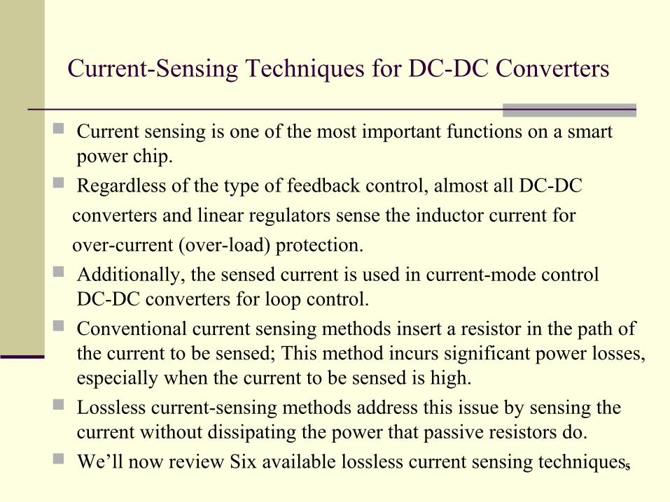
1. Series Sense Resistor
This technique is the conventional way of
sensing current. It simply inserts a Sense Resistor in series with
the inductor. If the value of the resistor is known, the current
flowing through the inductor is determined by sensing the voltage across it. This method obviously incurs a power loss in Rsense, and therefore reduces
the efficiency of the DC-DC converter. For accuracy, the voltage across the sense resistor should be roughly 100mV
at full load because of input-inferred offsets and other practical limitations. If full-load current is 1A, 0.1W is dissipated in the sense resistor. Main Disadvantage: For an output voltage of 3.3V, the output power
is 3.3W at full-load and hence the Sense Resistor reduces the system efficiency by 3.3%.
7
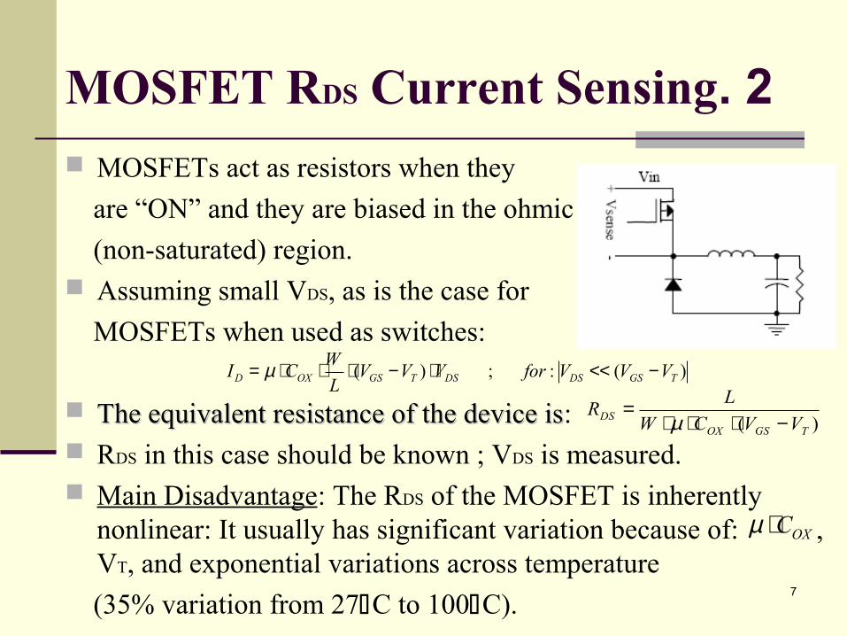
2. MOSFET RDS Current Sensing
MOSFETs act as resistors when they
are “ON” and they are biased in the ohmic
(non-saturated) region. Assuming small VDS, as is the case for
MOSFETs when used as switches:
The equivalent resistance of the device isThe equivalent resistance of the device is: RDS in this case should be known ; VDS is measured. Main Disadvantage: The RDS of the MOSFET is inherently
nonlinear: It usually has significant variation because of: , VT, and exponential variations across temperature
(35% variation from 27C to 100C).
)( TGSOXDS VVCW
LR
−⋅⋅⋅=
µ
)(:;)( TGSDSDSTGSOXD VVVforVVVL
WCI −<<⋅−⋅⋅⋅= µ
OXC⋅µ
8
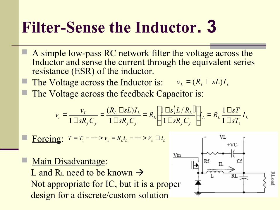
3. Filter-Sense the Inductor A simple low-pass RC network filter the voltage across the
Inductor and sense the current through the equivalent series resistance (ESR) of the inductor.
The Voltage across the Inductor is: The Voltage across the feedback Capacitor is:
Forcing:
Main Disadvantage: L and RL need to be known Not appropriate for IC, but it is a proper design for a discrete/custom solution
LLL IsLRv )( +=
( )LLL
ff
LL
ff
LL
ff
Lc I
sT
sTRI
CsR
RLsR
CsR
IsLR
CsR
vv
11
1
1
/1
1
)(
1 ++=
+
+=+
+=+
=
LcLLc iViRvTT ∝>−−−=>−−−= 1
9
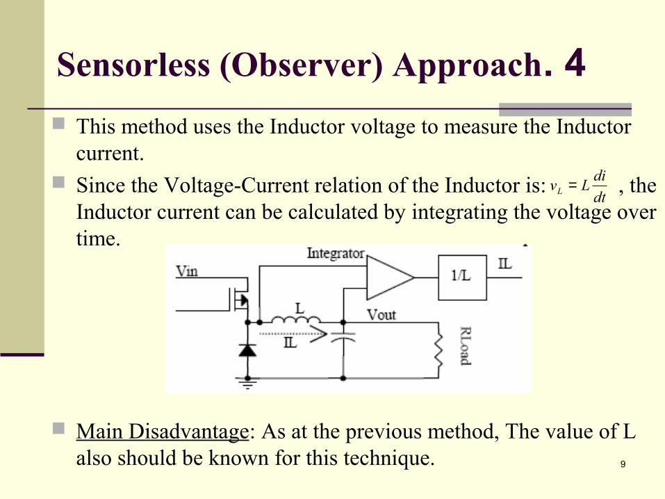
4. Sensorless (Observer) Approach
This method uses the Inductor voltage to measure the Inductor current.
Since the Voltage-Current relation of the Inductor is: , the Inductor current can be calculated by integrating the voltage over time.
Main Disadvantage: As at the previous method, The value of L also should be known for this technique.
dt
diLvL =
10
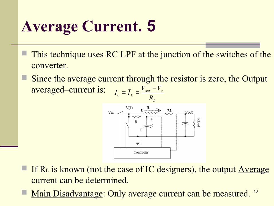
5. Average Current
This technique uses RC LPF at the junction of the switches of the converter.
Since the average current through the resistor is zero, the Output averaged–current is:
If RL is known (not the case of IC designers), the output Average current can be determined.
Main Disadvantage: Only average current can be measured.
L
coutLo R
VVII
−==

11
6. Current Transformers
The use of this technique is common in high power systems. The idea is to sense a fraction of the high Inductor current by
using the mutual inductor properties of a transformer. Main Disadvantages:
Increased cost and size and non-integrablity. The transformer also cannot transfer the DC portion of
current, which make this method inappropriate for
over current protection.

12
7. SENSEFETs This method is the practical technique for Current sensing in new
power MOSFET applications. The idea is to build a current sensing FET in parallel with the
power MOSFET (Current Mirror). The effective width (W) of the sense MOSFET (SENSEFET) is
significantly smaller than the power FET, and therefore linearly reduces ID per the MOSFET known equation:
The width (W) of the Power MOSFET is X100-1000 times the width of SENSEFET to guarantee it’s low power consumption.
DSTGSOXD VVVL
WCI ⋅−⋅⋅⋅= )(µ
The voltage of nodes M and Sshould be equal to eliminate the Current-Mirror non-idealityresulting from channel length modulation

13
Complete Current Sensing - SENSEFETs circuit
The Op amplifier is used to force VDS of M1 and M3 to be equal. As the width of the main MOSFET and SENSEFET increases, the accuracy of the circuit decreases. Main Disadvantage:
Relatively low Bandwidth Proper layout scheme should be designed to minimize coupling between
the transistor (which can induce significant error).
Advantages: Lossless Integrable Practical Relatively good accuracy
14
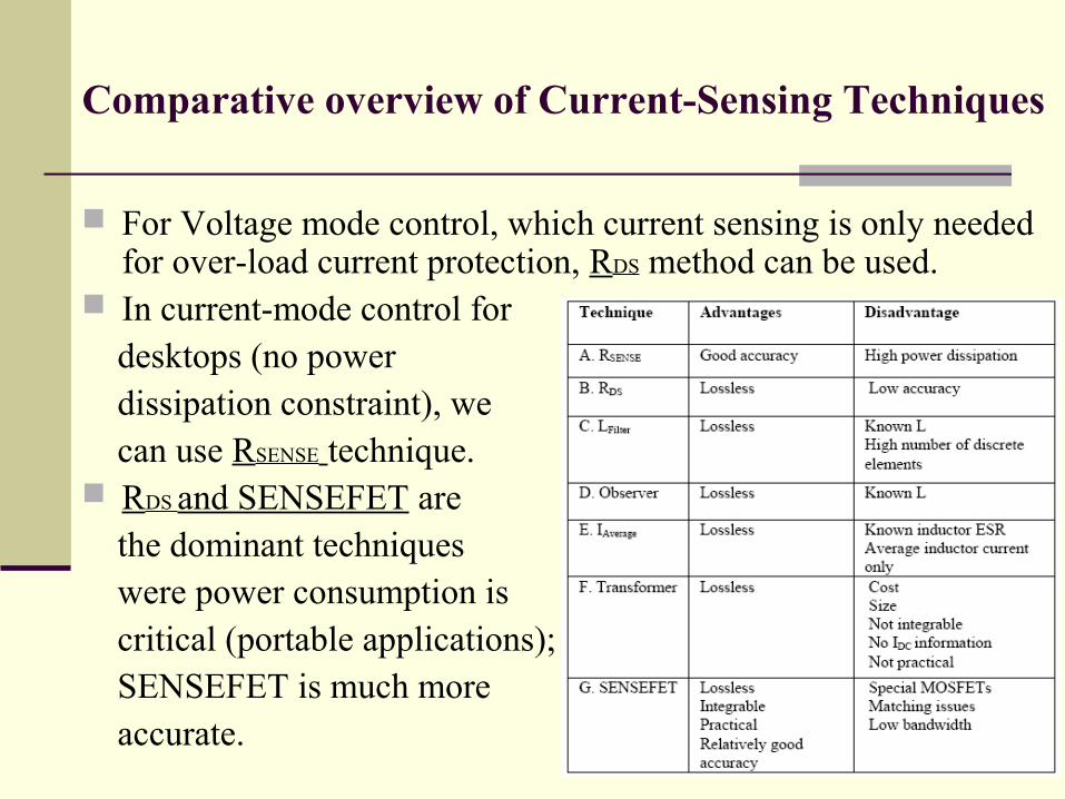
Comparative overview of Current-Sensing Techniques
For Voltage mode control, which current sensing is only needed for over-load current protection, RDS method can be used.
In current-mode control for desktops (no power dissipation constraint), we can use RSENSE technique. RDS and SENSEFET are the dominant techniques were power consumption is critical (portable applications); SENSEFET is much more accurate.
15
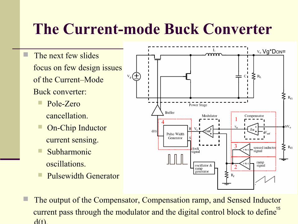
The Current-mode Buck Converter
The next few slides
focus on few design issues
of the Current–Mode
Buck converter: Pole-Zero
cancellation. On-Chip Inductor
current sensing. Subharmonic
oscillations. Pulsewidth Generator
The output of the Compensator, Compensation ramp, and Sensed Inductor
current pass through the modulator and the digital control block to define d(t).
= Vg*DON
1
3
2
4
16
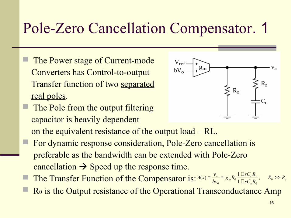
1. Pole-Zero Cancellation Compensator
The Power stage of Current-mode Converters has Control-to-output Transfer function of two separated real poles. The Pole from the output filtering capacitor is heavily dependent on the equivalent resistance of the output load – RL. For dynamic response consideration, Pole-Zero cancellation is preferable as the bandwidth can be extended with Pole-Zero cancellation Speed up the response time. The Transfer Function of the Compensator is: R0 is the Output resistance of the Operational Transconductance Amp
zc
zcm
a RRRsC
RsCRg
bv
vsA >>
++≈= 0
00
0
;1
1)(
17
Calculation of the two frequency compensation components – RZ , CC
The general purpose of introducing Zeros and Poles in the compensator is to cancel Poles and Zeros in the control-to-output function, respectively. This will yield an average -20 dB/decade closed-loop gain response with sufficient phase margin below the unity gain freq. When determining the unity gain frequency, it should not be too close to the converter’s switching frequency as the amplifier would amplify the output ripple voltage; A safe value of unity gain frequency is below 20% of the switching frequency. Since the dominant pole shifts inversely proportional to the load resistance, the lowest frequency occurs at the highest load resistance, two frequency compensation components - RZ and CC
can be calculated using the corresponding Transfer Function.
18
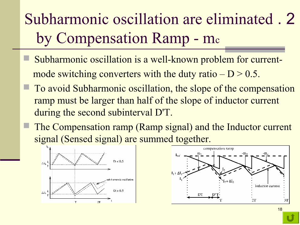
2. Subharmonic oscillation are eliminated by Compensation Ramp - mc
Subharmonic oscillation is a well-known problem for current-
mode switching converters with the duty ratio – D > 0.5. To avoid Subharmonic oscillation, the slope of the compensation
ramp must be larger than half of the slope of inductor current during the second subinterval D'T.
The Compensation ramp (Ramp signal) and the Inductor current signal (Sensed signal) are summed together.
19
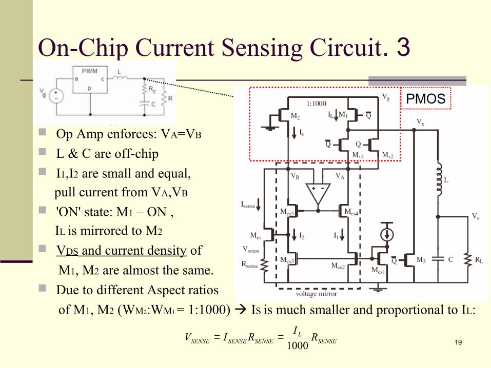
3. On-Chip Current Sensing Circuit
Op Amp enforces: VA=VB
L & C are off-chip I1,I2 are small and equal, pull current from VA,VB
'ON' state: M1 – ON , IL is mirrored to M2
VDS and current density of
M1, M2 are almost the same. Due to different Aspect ratios
of M1, M2 (WM2:WM1 = 1:1000) IS is much smaller and proportional to IL:
SENSEL
SENSESENSESENSE RI
RIV1000
==
PMOS
20
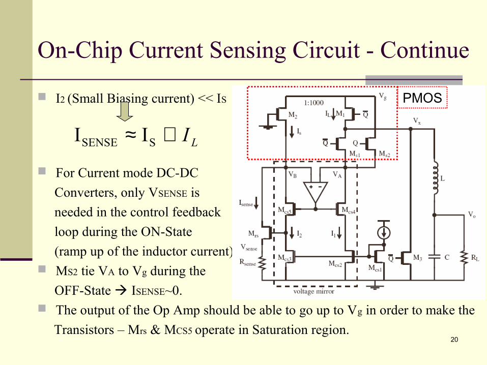
On-Chip Current Sensing Circuit - Continue
I2 (Small Biasing current) << IS
For Current mode DC-DC
Converters, only VSENSE is
needed in the control feedback
loop during the ON-State
(ramp up of the inductor current) MS2 tie VA to Vg during the
OFF-State ISENSE~0. The output of the Op Amp should be able to go up to Vg in order to make the
Transistors – Mrs & MCS5 operate in Saturation region.
LI∝≈ SSENSE II
PMOS

21
Current Sensing - Design Issues
The accuracy of the sensed Inductor current depends on the Current Mirror of transistors M1 and M2 and in the on-chip
Poly Resistor - RSENSE. The matching of transistors M1 and M2 depends on the process parameters such as Mobility, Oxide Capacitance (COX) and Threshold voltage (VT). Therefore, proper layout technique should be well considered, especially the location of the transistor M2, to minimize error. In the suggested design, M2 is surrounded by 500 fingers of M1. Of course, This on-chip current-sensing circuit can be extended to sense power NMOS transistor by simply building a complement circuit for other topologies (as Boost, Buck-Boost).

22
Pulsewidth Generator
This Implementation deals with the Startup situation in which both inputs are high In this situation, the Latch is SET.

23
Measurements Results - 1 The Converter is supplied with an Input voltage of 3.6V,
and Switching frequency of 500KHz. Attached Steady-state measurements with:
Maximum Loading current = 300mA ; RSENSE = 400 Ohm Output voltage = 2.1V and Duty Ratio > 0.5 (Subharmonic oscillation zone)
Inductor Current
Sensing Voltage
Inductor Current
Inductor Voltage (Vx)

24
Measurements Results - 1
DC Output Voltage = 2.12V Output Ripple Voltage = 6.4mV
25
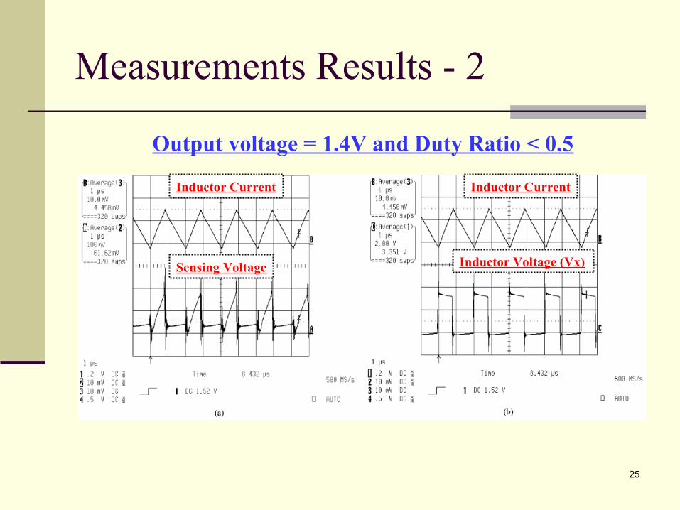
Measurements Results - 2
Output voltage = 1.4V and Duty Ratio < 0.5
Inductor Current
Sensing Voltage
Inductor Current
Inductor Voltage (Vx)
26
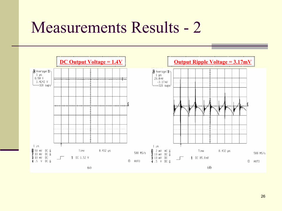
Measurements Results - 2
DC Output Voltage = 1.4V Output Ripple Voltage = 3.17mV
27
Circuit Efficiency and Performance
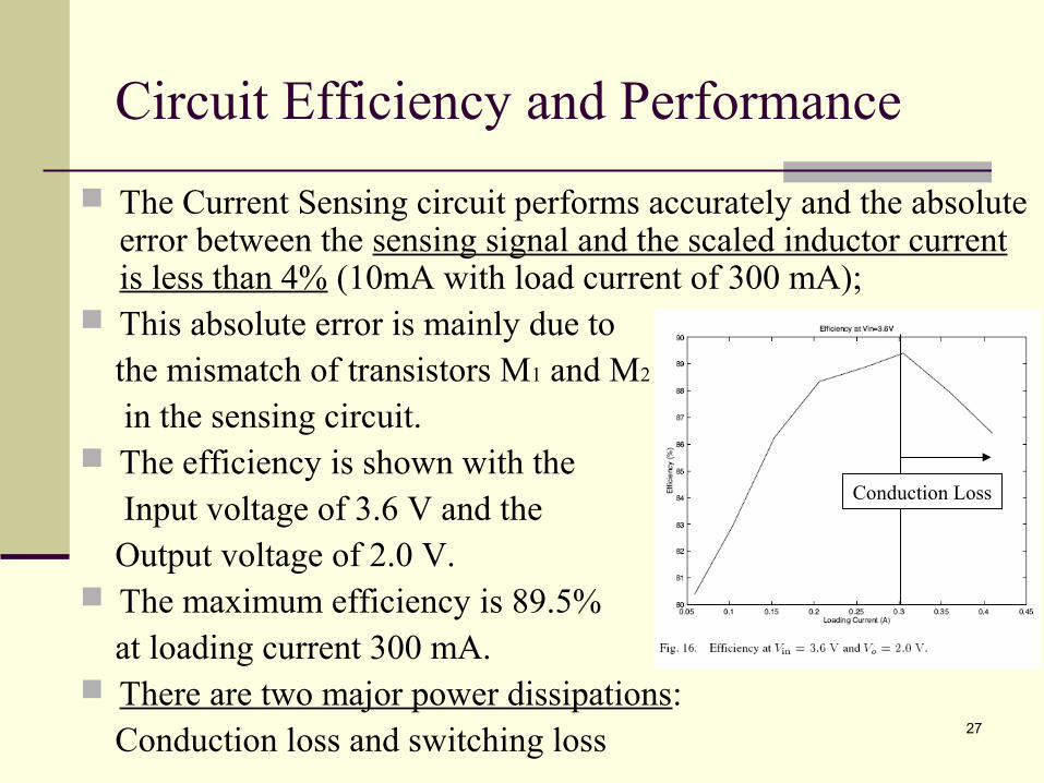
The Current Sensing circuit performs accurately and the absolute error between the sensing signal and the scaled inductor current is less than 4% (10mA with load current of 300 mA);
This absolute error is mainly due to the mismatch of transistors M1 and M2 in the sensing circuit. The efficiency is shown with the Input voltage of 3.6 V and the Output voltage of 2.0 V. The maximum efficiency is 89.5% at loading current 300 mA. There are two major power dissipations: Conduction loss and switching loss
Conduction Loss
28
Conclusions & Summary Experimental results show that the converter regulates properly with duty ratio – D larger and smaller than 0.5. Using the internal Current-Sensing technique, it not only reduces the external pins for the monolithic controller, but also reduces the complexity of the design. Due to the accurate Sensing performance, a compensation ramp can be added to the sensing signal without any consideration on the variation of the sensing performance. The accurately sensed Inductor current can also be used for over-current protection and Load-dependent mode-hopping schemes for optimizing power efficiency. In addition, this current-mode DC–DC buck converter with internal current sensor can operate from 300 kHz to 1MHz with the input voltage range from 3 to 5.2 V, which is suitable for lithium-ion battery supply applications.
29
References
A Monolithic Current-Mode CMOS DC–DC Converter With On-Chip Current-Sensing Technique.
Cheung Fai Lee and Philip K. T. Mok, Senior Member, IEEE, IEEE JOURNAL OF SOLID-STATE CIRCUITS, VOL. 39,
NO. 1, JANUARY 2004. On-Chip Current Sensing Technique for CMOS Monolithic
Switch-Mode Power Converters. Cheung Fai Lee and Philip K. T. Mok, In IEEE Int. Symp. Circuits and Systems, vol. 5, Scottsdale, AZ,
May 2002, pp. 265–268. Current-Sensing Techniques for DC-DC Converters. Hassan Pooya Forghani-zadeh, Student member, IEEE, and
Gabriel A. Rincón-Mora, Senior member, IEEE, Georgia Tech Analog Consortium.

30