Embed Size (px)
Citation preview
Simulation Strategies for Massively Parallel
Supercomputer Design
Authored by:Ansoft Corporation
Ansoft 2003 / Global Seminars: Delivering PerformancePresentation #2
Special Thanks to:Cray
Introduction
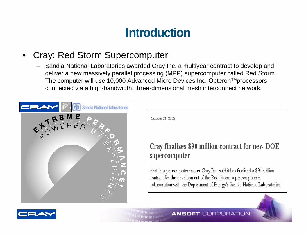
• Cray: Red Storm Supercomputer– Sandia National Laboratories awarded Cray Inc. a multiyear contract to develop and
deliver a new massively parallel processing (MPP) supercomputer called Red Storm. The computer will use 10,000 Advanced Micro Devices Inc. Opteron™ processors connected via a high-bandwidth, three-dimensional mesh interconnect network.
Introduction
• About Cray– Approximately 850 employees worldwide
– Corporate headquarters: Seattle, WA
– 3 major engineering centers: • Chippewa Falls, WI, • Mendota Heights, MN, • Seattle, WA
– NASDAQ: CRAY
Introduction
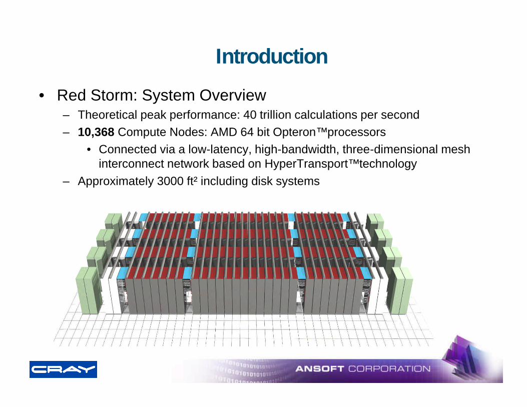
• Red Storm: System Overview– Theoretical peak performance: 40 trillion calculations per second– 10,368 Compute Nodes: AMD 64 bit Opteron™ processors
• Connected via a low-latency, high-bandwidth, three-dimensional mesh interconnect network based on HyperTransport™ technology
– Approximately 3000 ft² including disk systems
Introduction
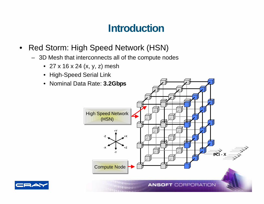
• Red Storm: High Speed Network (HSN)– 3D Mesh that interconnects all of the compute nodes
• 27 x 16 x 24 (x, y, z) mesh• High-Speed Serial Link• Nominal Data Rate: 3.2Gbps
PCI - X
+Y
-Y
+Z-X
+X-Z
+Y
-Y
+Z-X
+X-Z
Compute NodeCompute Node
High Speed Network(HSN)
High Speed Network(HSN)
Introduction
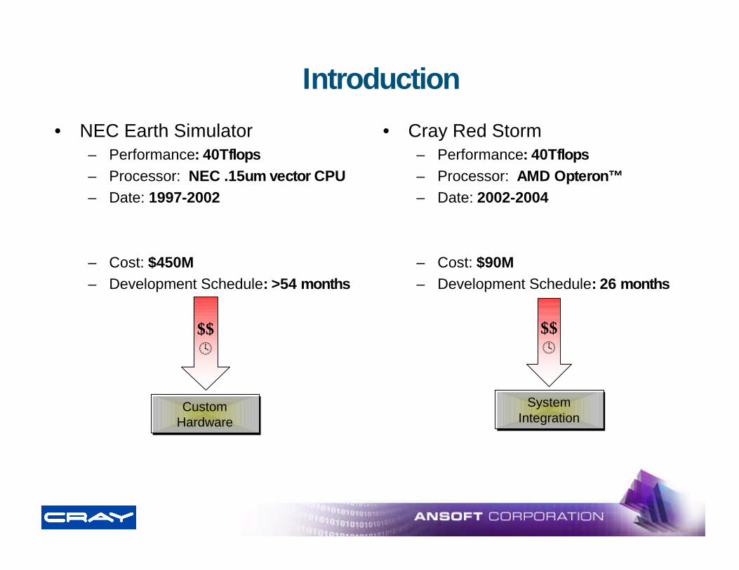
• NEC Earth Simulator– Performance: 40Tflops– Processor: NEC .15um vector CPU– Date: 1997-2002
– Cost: $450M– Development Schedule: >54 months
• Cray Red Storm– Performance: 40Tflops– Processor: AMD Opteron™– Date: 2002-2004
– Cost: $90M– Development Schedule: 26 months
$$º
$$º
Custom HardwareCustom
HardwareSystem
IntegrationSystem
Integration
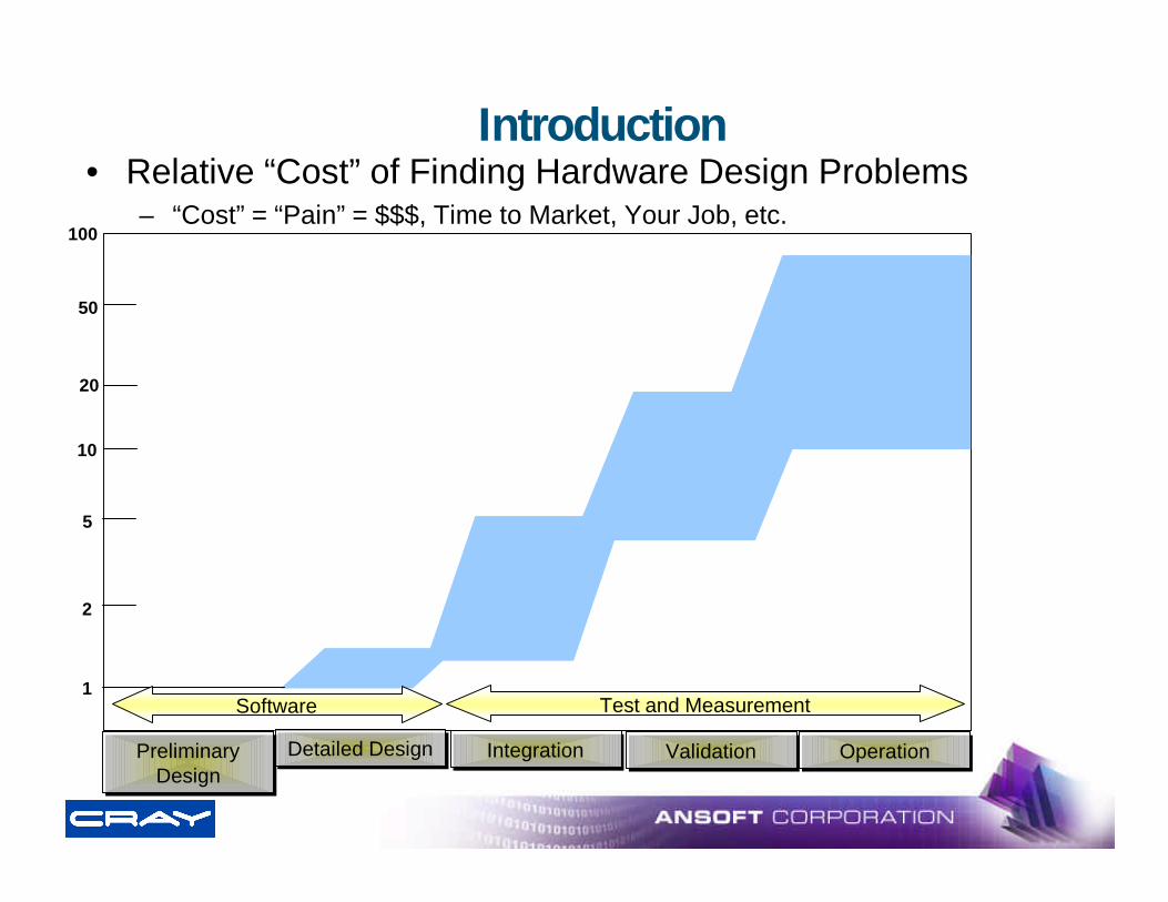
Introduction• Relative “Cost” of Finding Hardware Design Problems
– “Cost” = “Pain” = $$$, Time to Market, Your Job, etc.
Detailed DesignDetailed Design IntegrationIntegration ValidationValidation OperationOperationPreliminary Design
Preliminary Design
1
2
5
10
20
50
100
Software Test and Measurement
Introduction
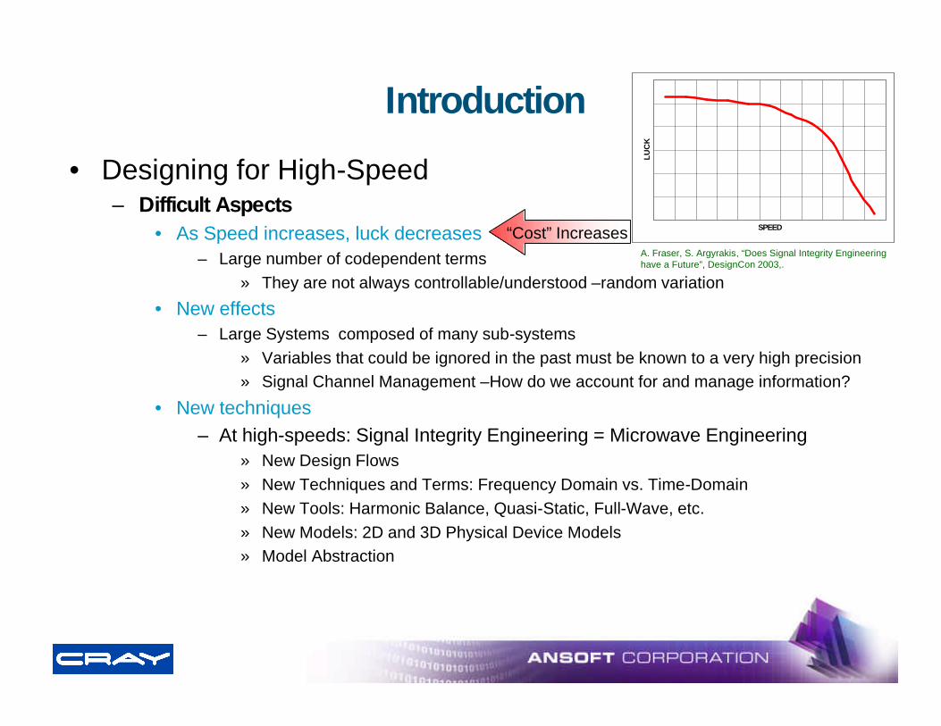
• Designing for High-Speed– Difficult Aspects
• As Speed increases, luck decreases– Large number of codependent terms
» They are not always controllable/understood – random variation
• New effects– Large Systems composed of many sub-systems
» Variables that could be ignored in the past must be known to a very high precision» Signal Channel Management – How do we account for and manage information?
• New techniques– At high-speeds: Signal Integrity Engineering = Microwave Engineering
» New Design Flows» New Techniques and Terms: Frequency Domain vs. Time-Domain» New Tools: Harmonic Balance, Quasi-Static, Full-Wave, etc.» New Models: 2D and 3D Physical Device Models» Model Abstraction
“Cost” Increases SPEED
LU
CK
A. Fraser, S. Argyrakis, “Does Signal Integrity Engineering have a Future”, DesignCon 2003,.
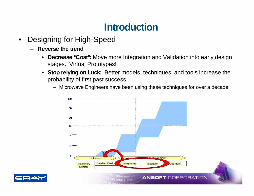
Introduction• Designing for High-Speed
– Reverse the trend• Decrease “Cost”: Move more Integration and Validation into early design
stages. Virtual Prototypes!• Stop relying on Luck: Better models, techniques, and tools increase the
probability of first past success.– Microwave Engineers have been using these techniques for over a decade
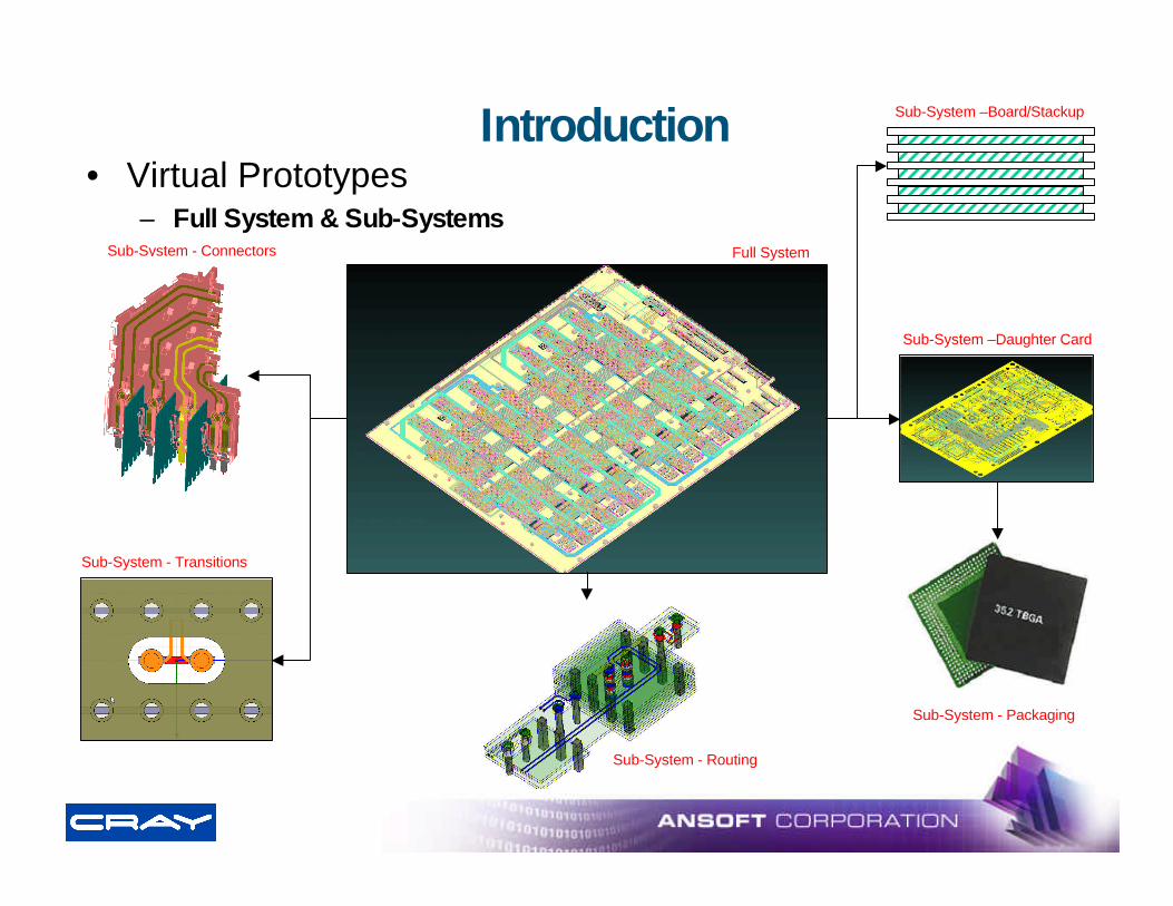
Introduction• Virtual Prototypes
– Full System & Sub-SystemsFull System
Sub-System - Routing
Sub-System - Transitions
Sub-System - Connectors
Sub-System - Packaging
Sub-System – Board/Stackup
Sub-System – Daughter Card
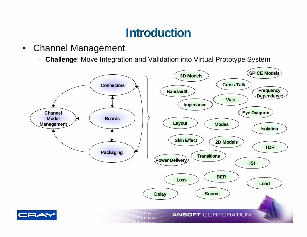
Introduction• Channel Management
– Challenge: Move Integration and Validation into Virtual Prototype System
ChannelModel
Management
Connectors
Boards
Packaging
Isolation
TransitionsPower Delivery
Vias
Modes
BandwidthCross-Talk
Layout
BERLoss
Skin Effect
Eye Diagram
ISI
Impedance
Load
Source
3D Models SPICE Models
2D Models
Frequency Dependence
TDR
Delay
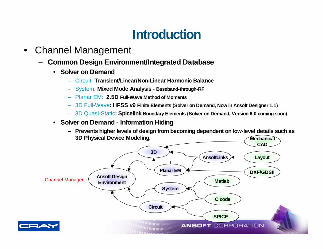
Introduction• Channel Management
– Common Design Environment/Integrated Database• Solver on Demand
– Circuit: Transient/Linear/Non-Linear Harmonic Balance– System: Mixed Mode Analysis - Baseband-through-RF
– Planar EM: 2.5D Full-Wave Method of Moments
– 3D Full-Wave: HFSS v9 Finite Elements (Solver on Demand, Now in Ansoft Designer 1.1)
– 3D Quasi-Static: Spicelink Boundary Elements (Solver on Demand, Version 6.0 coming soon)
• Solver on Demand - Information Hiding– Prevents higher levels of design from becoming dependent on low-level details such as
3D Physical Device Modeling.
Ansoft DesignEnvironmentChannel Manager
Circuit
System
Planar EM
3DLayoutAnsoftLinks
MechanicalCAD
DXF/GDSII
SPICE
Matlab
C code
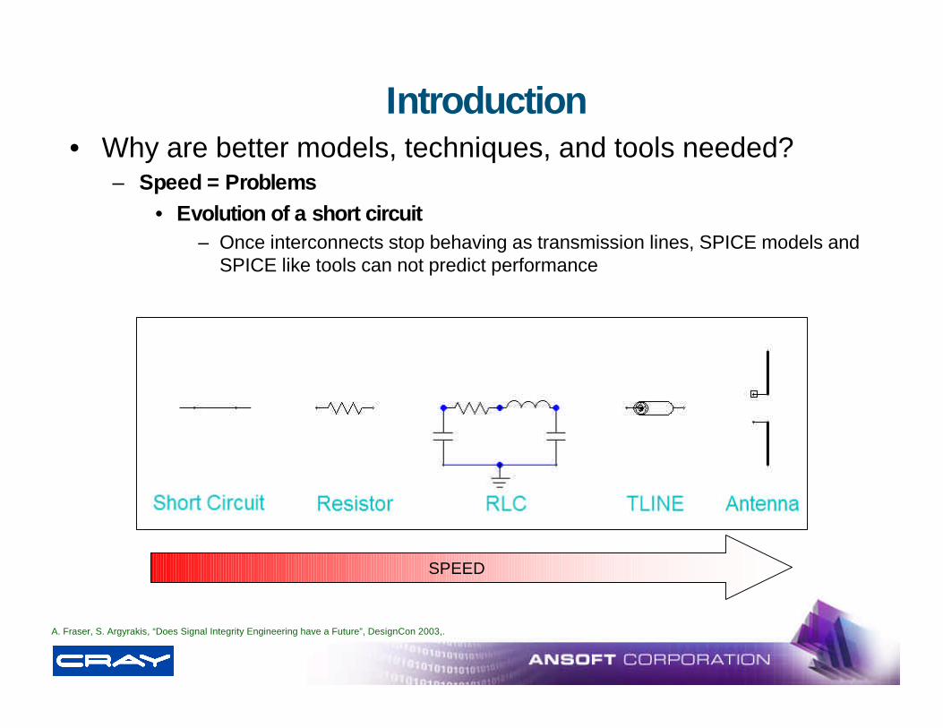
Introduction• Why are better models, techniques, and tools needed?
– Speed = Problems• Evolution of a short circuit
– Once interconnects stop behaving as transmission lines, SPICE models and SPICE like tools can not predict performance
SPEED
A. Fraser, S. Argyrakis, “Does Signal Integrity Engineering have a Future”, DesignCon 2003,.
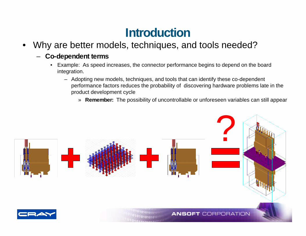
Introduction• Why are better models, techniques, and tools needed?
– Co-dependent terms• Example: As speed increases, the connector performance begins to depend on the board
integration.– Adopting new models, techniques, and tools that can identify these co-dependent
performance factors reduces the probability of discovering hardware problems late in the product development cycle
» Remember: The possibility of uncontrollable or unforeseen variables can still appear
?
Introduction
• What are these uncontrollable or unforeseen variables?– Virtual Prototypes are abstractions
• They only contain the essential details of a complex system– Essential Details = Those that are critical to the electrical performance– Model Abstraction efficiently uses limited computer resources and product
development time– Example: Cavity filter designers routinely use screws to tune the filter and
account for manufacturing variations. When they simulate their filter designs they would not include the threads on the screw. The threads are essential mechanical details, not electrical details
– Manufacturing Process Variations • Example: If the virtual prototype does not account for the substrate
thickness shrinking because of thermal effects in the manufacturing process, you will not predict the performance correctly.
Introduction
• Ansoft and Cray– Ansoft: Provide End-to-End Simulations of HSN Channel
• Five different classes of simulations / analysis1. PCB/Interconnects
– Mezzanine, Module, Backplane, and Red/Black Switch
2. Connectors– NexLev, GbX, and VHDM
3. Cabling– Self-Equalizing Twin-Ax (1.1m - 8m)
4. Packaging– HyperBGA – High Performance Organic Flip-Chip BGA
5. System– Frequency and Time Based Performance Extraction
– Cray: Provide• Electrical Specifications• Electrical Models• Mechanical Models• Board Layouts
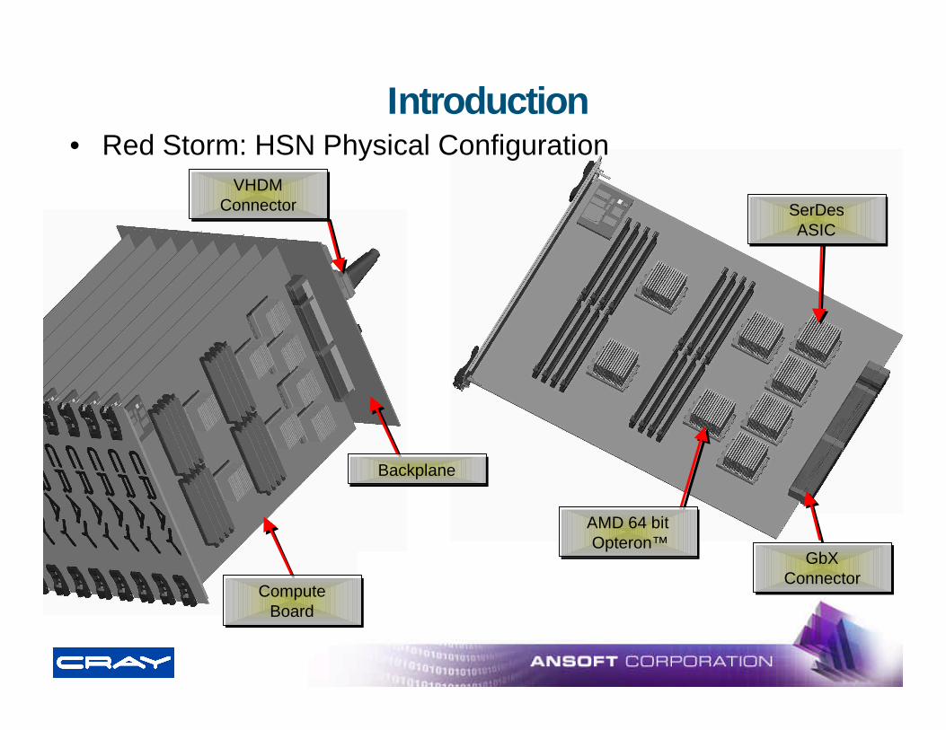
• Red Storm: HSN Physical ConfigurationIntroduction
BackplaneBackplane
ComputeBoard
ComputeBoard
VHDM Connector
VHDM Connector
GbXConnector
GbXConnector
SerDesASIC
SerDesASIC
AMD 64 bit Opteron™
AMD 64 bit Opteron™

Introduction• Red Storm: HSN Electrical Configuration
HyperBGA+
Mezzanine Board
ModuleBoard Backplane Red/Black
Switch
Connector Connector ConnectorCable
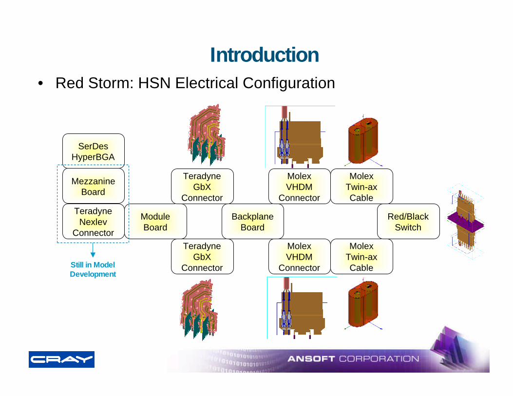
Introduction• Red Storm: HSN Electrical Configuration
ModuleBoard
TeradyneGbX
Connector
BackplaneBoard
MolexVHDM
Connector
MolexTwin-axCable
Red/BlackSwitch
TeradyneGbX
Connector
MolexVHDM
Connector
MolexTwin-axCable
SerDesHyperBGA
TeradyneNexlev
Connector
MezzanineBoard
Still in Model Development
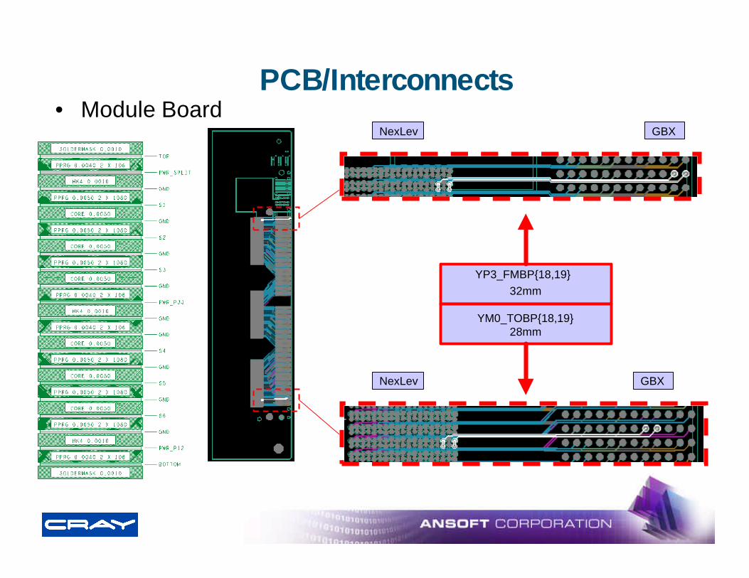
PCB/Interconnects• Module Board
YP3_FMBP{18,19}32mm
YM0_TOBP{18,19}28mm
GBXNexLev
NexLev GBX
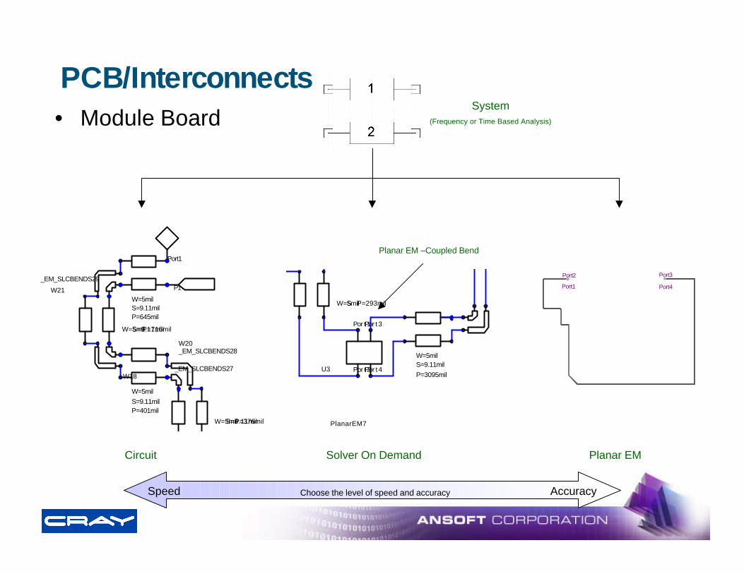
PCB/Interconnects• Module Board
System(Frequency or Time Based Analysis)
Circuit Solver On Demand Planar EM
Speed AccuracyChoose the level of speed and accuracy
Planar EM – Coupled Bend
Port1
Port2 Port3
Port4
Port1
P1
S=9.11milW=5milP=376mil
S=9.11milW=5milP=716mil
W18_EM_SLCBENDS27
S=9.11milW=5mil
P=401mil
W20_EM_SLCBENDS28
W21
_EM_SLCBENDS29
S=9.11milW=5mil
P=645mil
S=9.11milW=5mil
P=3095mil
S=9.11milW=5milP=293mil
Por t 1
Por t 2
Por t 3
Por t 4U3
PlanarEM7
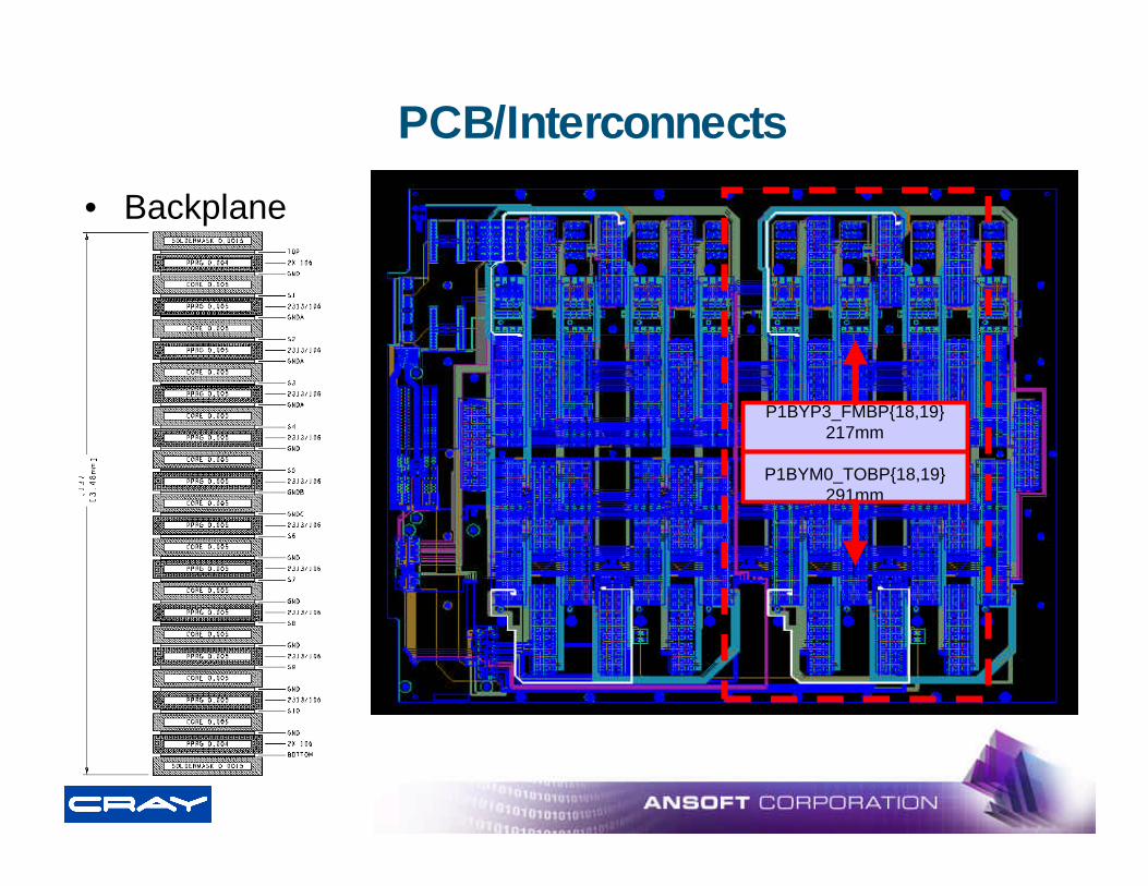
PCB/Interconnects
• Backplane
P1BYP3_FMBP{18,19}217mm
P1BYM0_TOBP{18,19}291mm
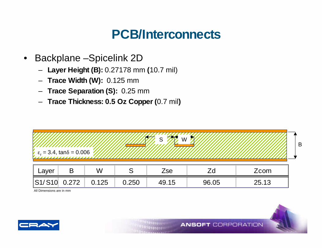
PCB/Interconnects
• Backplane – Spicelink 2D– Layer Height (B): 0.27178 mm (10.7 mil)– Trace Width (W): 0.125 mm– Trace Separation (S): 0.25 mm– Trace Thickness: 0.5 Oz Copper (0.7 mil)
BS W
εr = 3.4, tanδ = 0.006
Layer B W S Zse Zd Zcom
S1/ S10 0.272 0.125 0.250 49.15 96.05 25.13All Dimensions are in mm
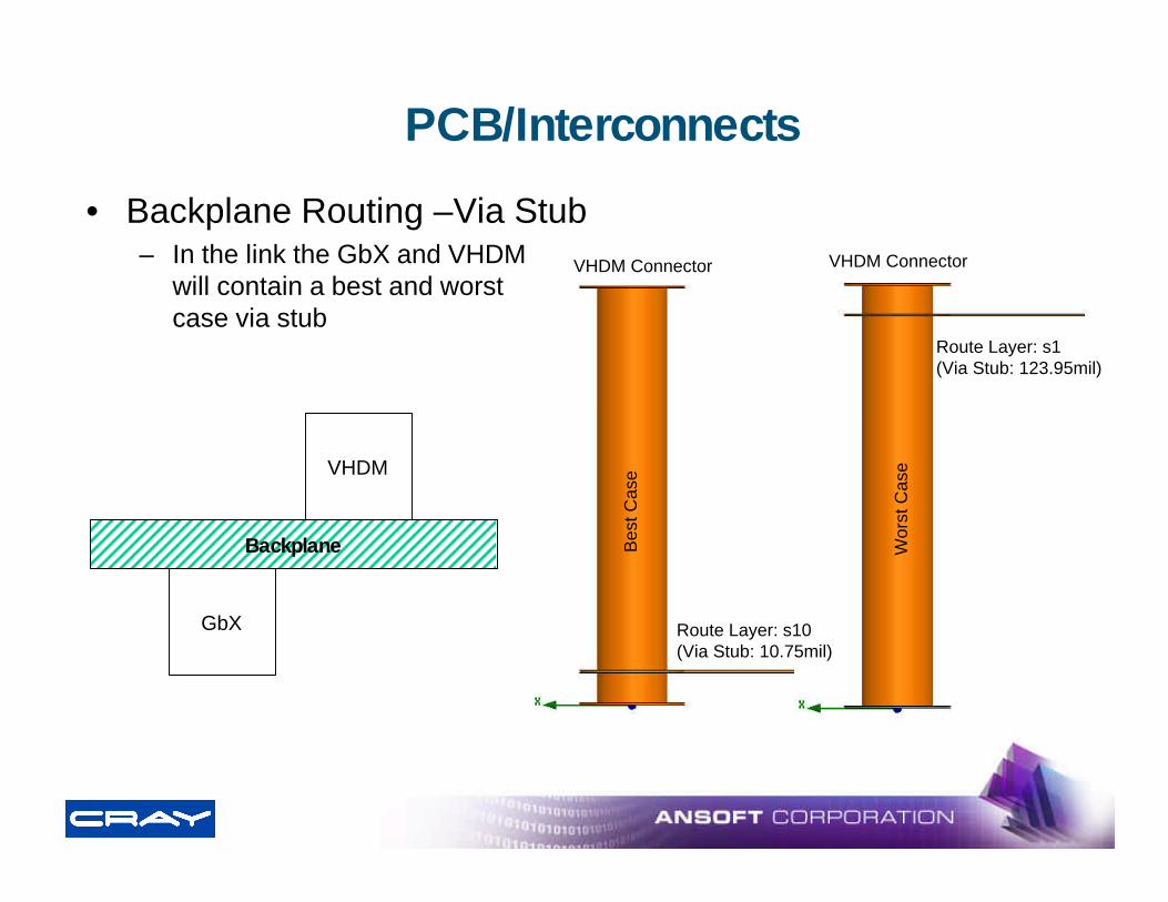
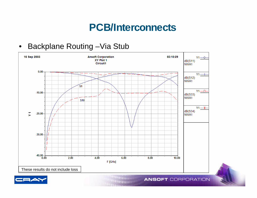
PCB/Interconnects
• Backplane Routing – Via Stub– In the link the GbX and VHDM
will contain a best and worst case via stub
Route Layer: s10(Via Stub: 10.75mil)
Route Layer: s1(Via Stub: 123.95mil)
VHDM Connector VHDM Connector
Bes
t Cas
e
Wor
st C
ase
Backplane
VHDM
GbX
PCB/Interconnects
• Backplane Routing – Via Stub
These results do not include loss
PCB/Interconnects
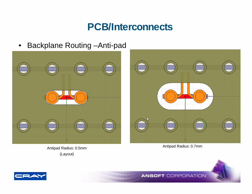
• Backplane Routing – Anti-pad
Antipad Radius: 0.5mm
(Layout)
Antipad Radius: 0.7mm
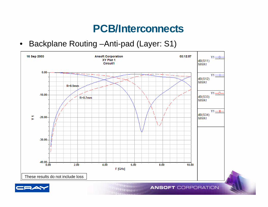
PCB/Interconnects• Backplane Routing – Anti-pad (Layer: S1)
These results do not include loss
PCB/Interconnects
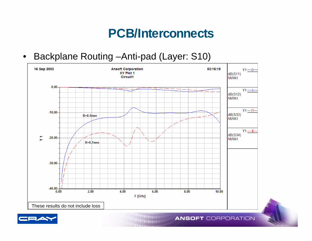
• Backplane Routing – Anti-pad (Layer: S10)
These results do not include loss
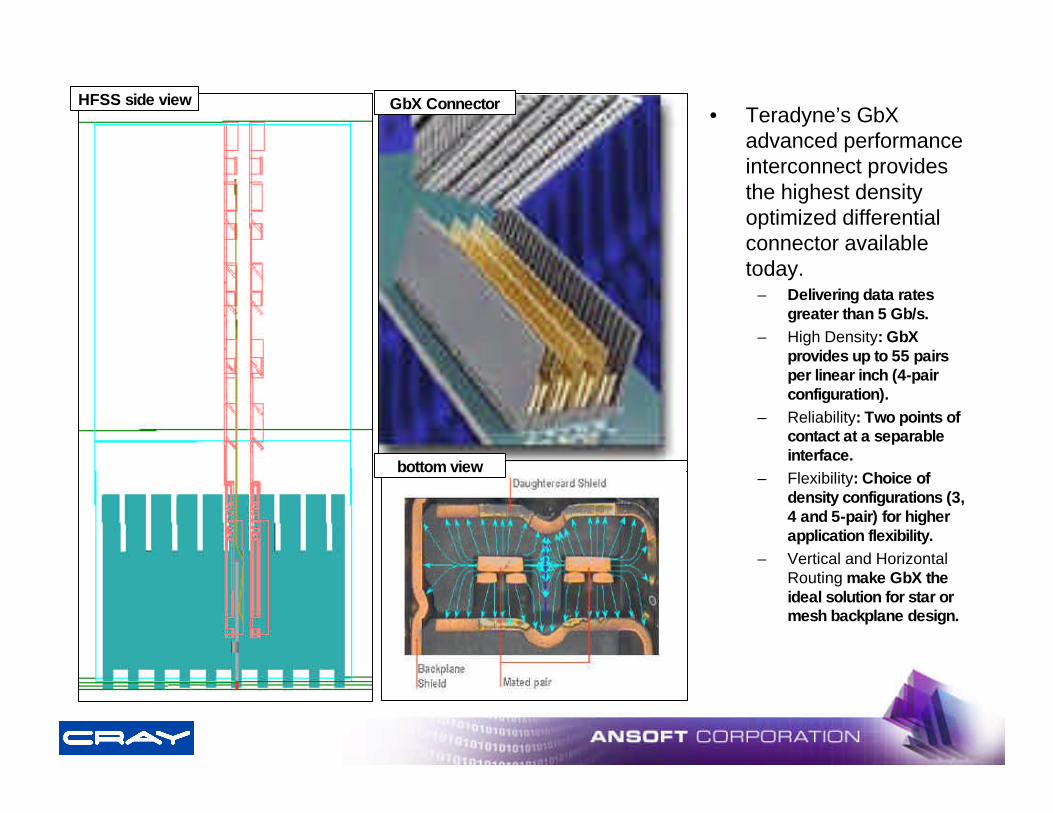
• Teradyne’s GbXadvanced performance interconnect provides the highest density optimized differential connector available today.
– Delivering data rates greater than 5 Gb/s.
– High Density: GbXprovides up to 55 pairs per linear inch (4-pair configuration).
– Reliability: Two points of contact at a separable interface.
– Flexibility: Choice of density configurations (3, 4 and 5-pair) for higher application flexibility.
– Vertical and Horizontal Routing make GbX the ideal solution for star or mesh backplane design.
HFSS side view
bottom view
GbX Connector
Connectors
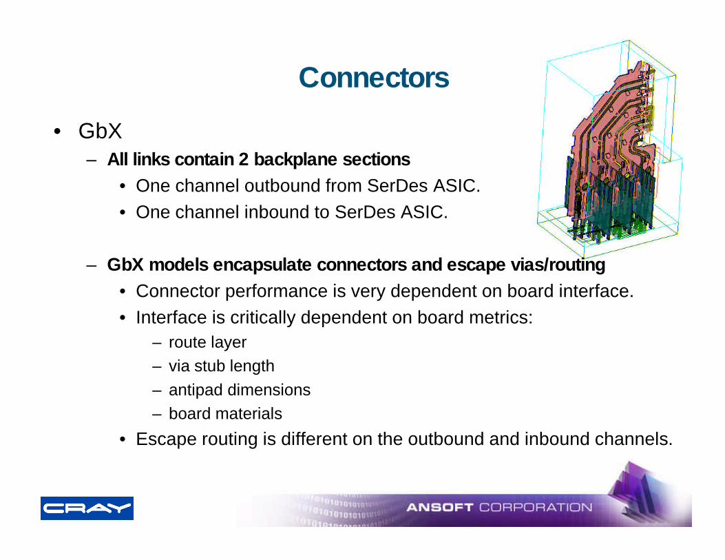
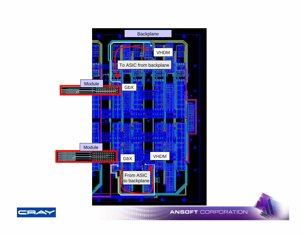
• GbX– All links contain 2 backplane sections
• One channel outbound from SerDes ASIC.• One channel inbound to SerDes ASIC.
– GbX models encapsulate connectors and escape vias/routing• Connector performance is very dependent on board interface.• Interface is critically dependent on board metrics:
– route layer– via stub length– antipad dimensions– board materials
• Escape routing is different on the outbound and inbound channels.
GbX
VHDM
VHDM
To ASIC from backplane
From ASIC to backplane
GbX
Backplane
Module
Module
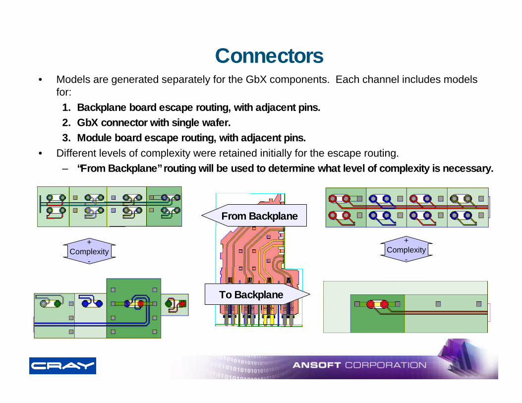
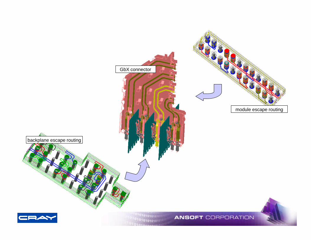
Connectors• Models are generated separately for the GbX components. Each channel includes models
for:1. Backplane board escape routing, with adjacent pins.2. GbX connector with single wafer.3. Module board escape routing, with adjacent pins.
• Different levels of complexity were retained initially for the escape routing.– “From Backplane” routing will be used to determine what level of complexity is necessary.
To Backplane
From Backplane
+Complexity
-
+Complexity
-
backplane escape routing
GbX connector
module escape routing
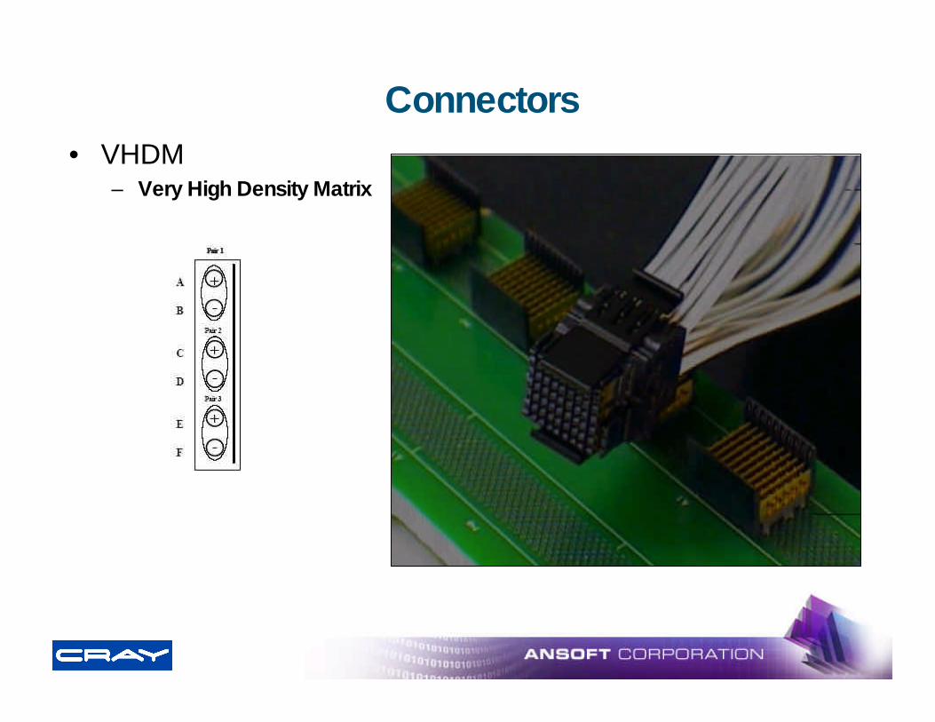
Connectors• VHDM
– Very High Density Matrix
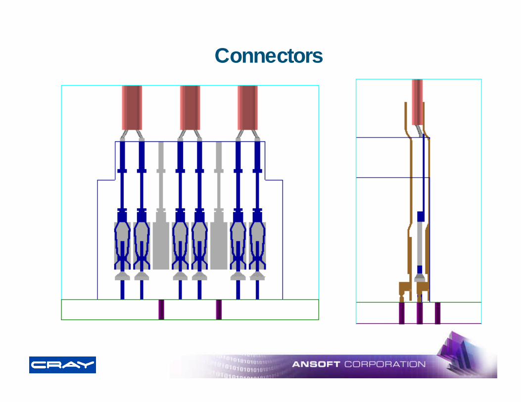
Connectors
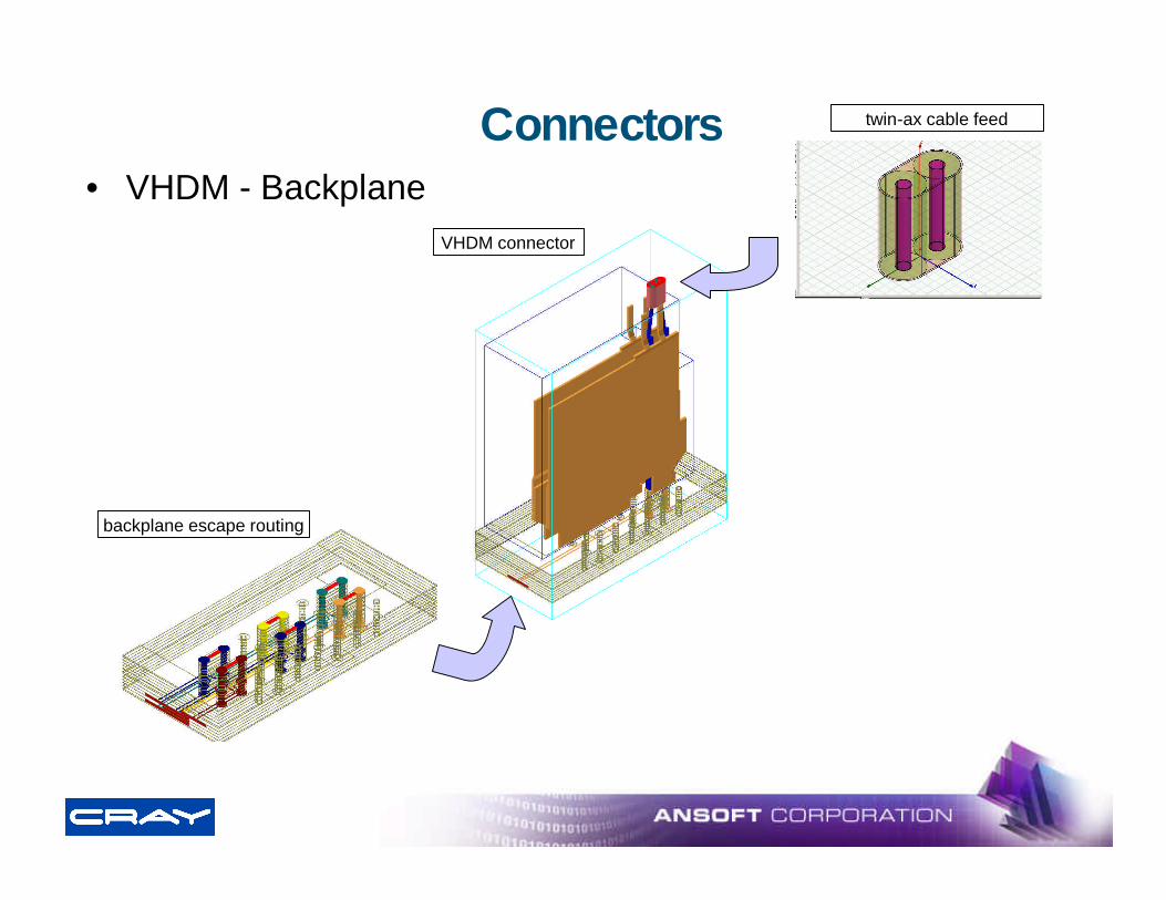
Connectors• VHDM - Backplane
backplane escape routing
VHDM connector
twin-ax cable feed
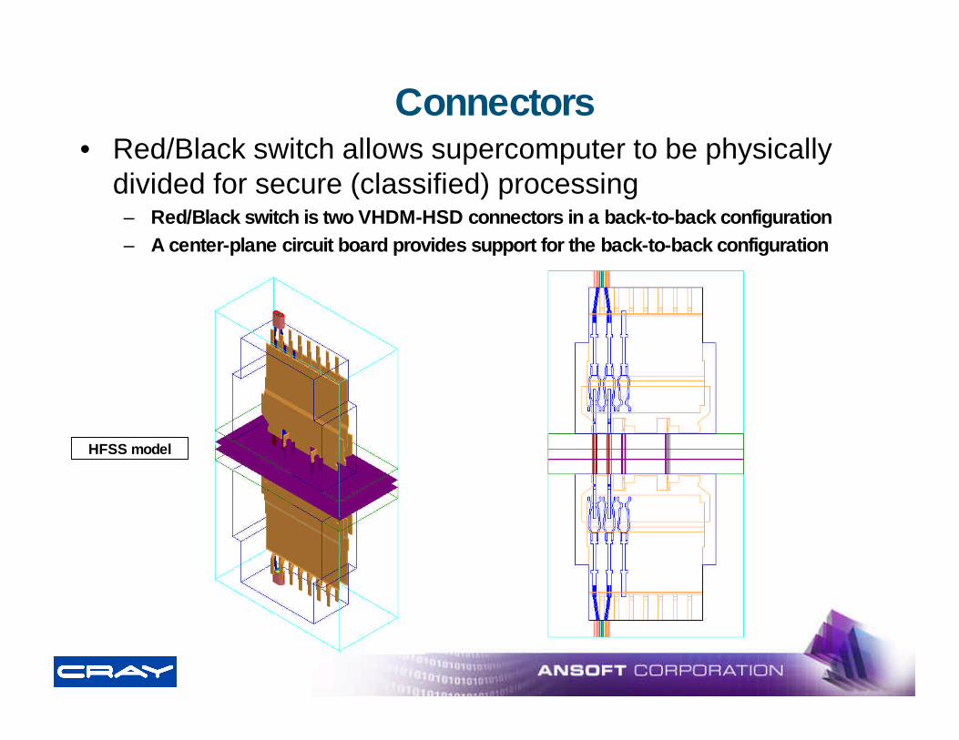
Connectors• Red/Black switch allows supercomputer to be physically
divided for secure (classified) processing– Red/Black switch is two VHDM-HSD connectors in a back-to-back configuration– A center-plane circuit board provides support for the back-to-back configuration
HFSS model
Cable
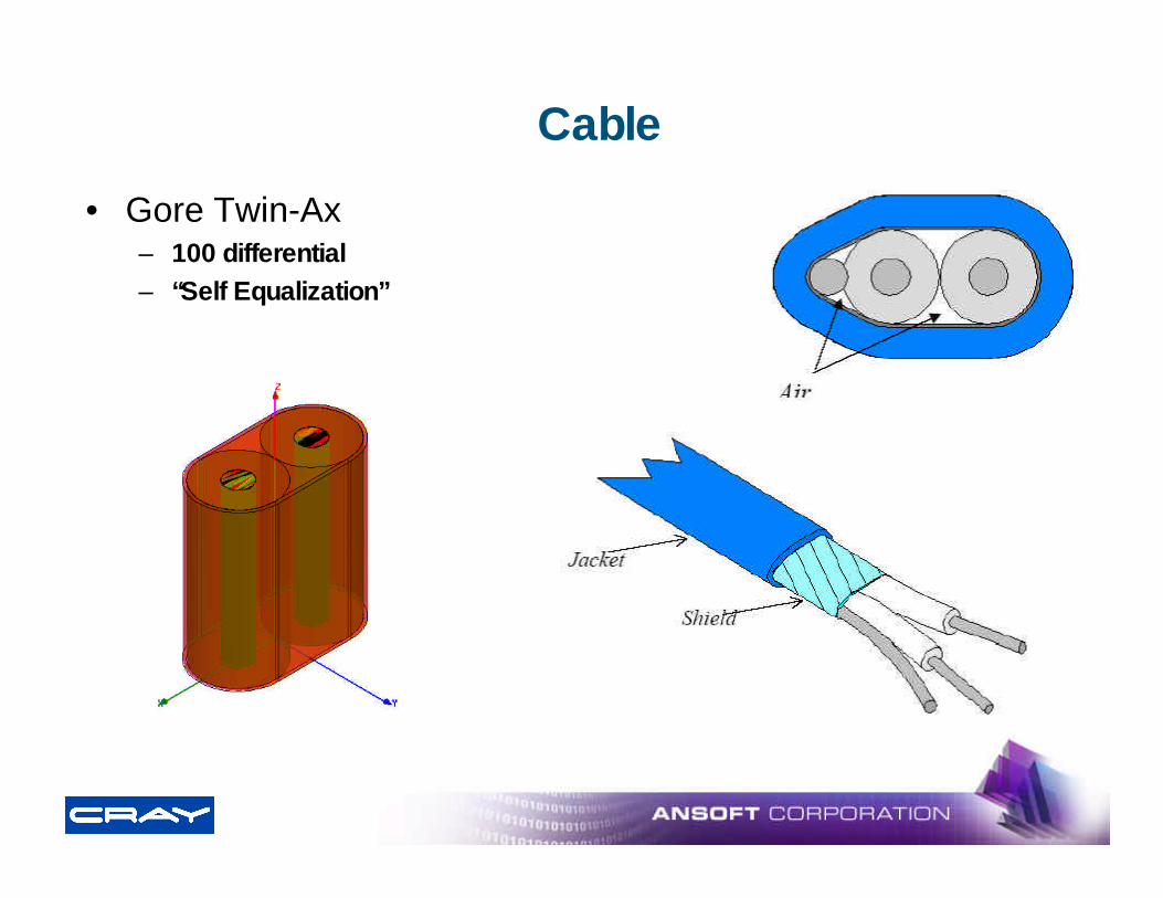
• Gore Twin-Ax– 100 differential– “Self Equalization”
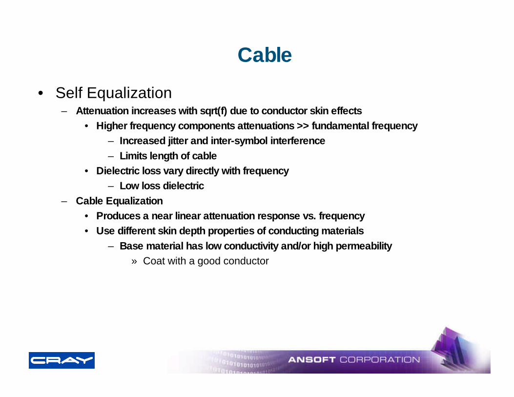
Cable
• Self Equalization– Attenuation increases with sqrt(f) due to conductor skin effects
• Higher frequency components attenuations >> fundamental frequency– Increased jitter and inter-symbol interference– Limits length of cable
• Dielectric loss vary directly with frequency– Low loss dielectric
– Cable Equalization• Produces a near linear attenuation response vs. frequency• Use different skin depth properties of conducting materials
– Base material has low conductivity and/or high permeability» Coat with a good conductor
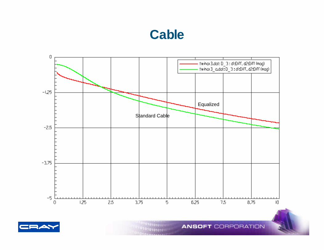
Cable
Standard Cable
Equalized
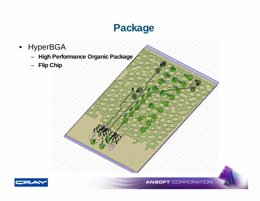
Package
• HyperBGA– High Performance Organic Package– Flip Chip
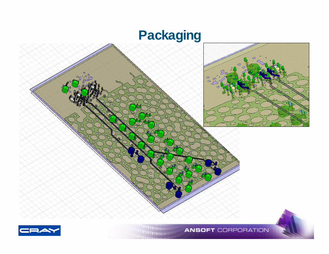
Packaging
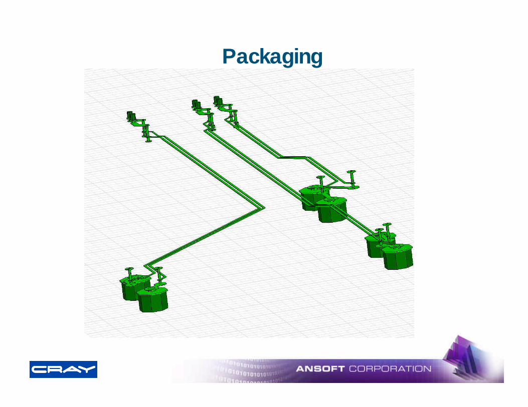
Packaging
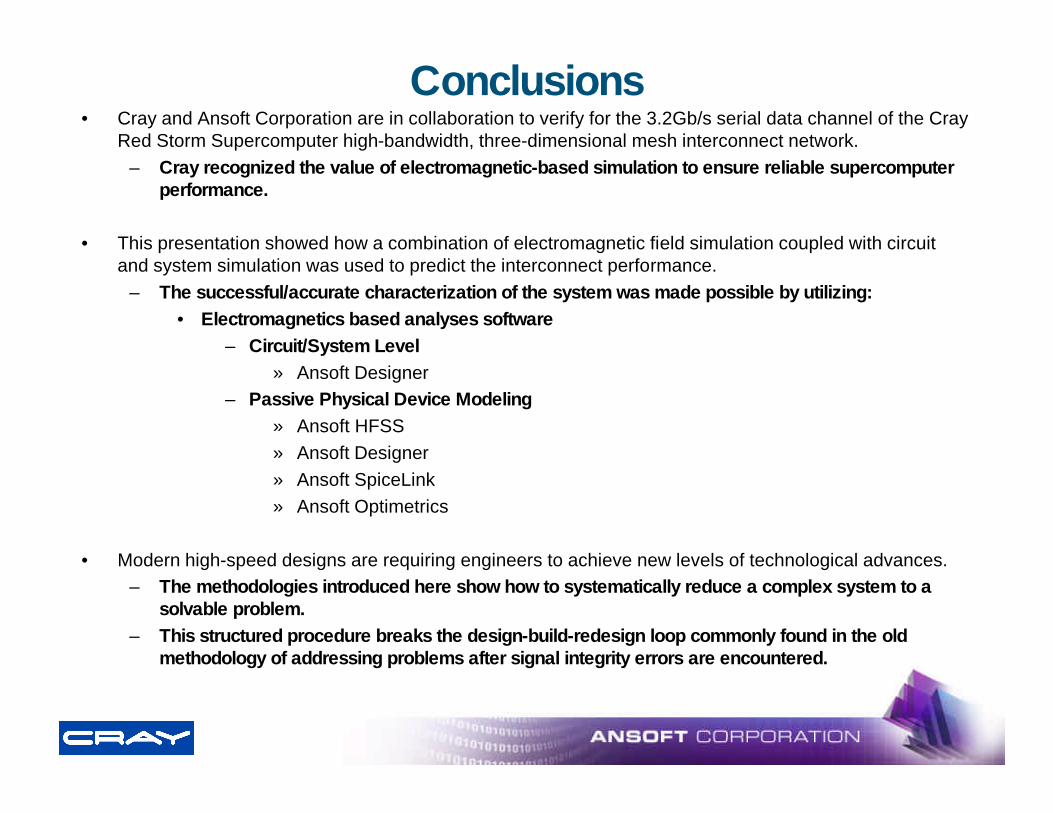
Conclusions• Cray and Ansoft Corporation are in collaboration to verify for the 3.2Gb/s serial data channel of the Cray
Red Storm Supercomputer high-bandwidth, three-dimensional mesh interconnect network.– Cray recognized the value of electromagnetic-based simulation to ensure reliable supercomputer
performance.
• This presentation showed how a combination of electromagnetic field simulation coupled with circuit and system simulation was used to predict the interconnect performance.
– The successful/accurate characterization of the system was made possible by utilizing:• Electromagnetics based analyses software
– Circuit/System Level» Ansoft Designer
– Passive Physical Device Modeling» Ansoft HFSS » Ansoft Designer» Ansoft SpiceLink» Ansoft Optimetrics
• Modern high-speed designs are requiring engineers to achieve new levels of technological advances. – The methodologies introduced here show how to systematically reduce a complex system to a
solvable problem.– This structured procedure breaks the design-build-redesign loop commonly found in the old
methodology of addressing problems after signal integrity errors are encountered.


![Molecular dynamics simulation of water permeation through ...nht.xjtu.edu.cn/paper/en/20162014.pdf · The large-scale atomic/molecular massively parallel simulation (LAMMPS) [34]](https://img.pdfslide.us/doc/110x75/60420f90865780693b58e984/molecular-dynamics-simulation-of-water-permeation-through-nhtxjtueducnpaperen.jpg)


![[1cm] A Massively-Parallel Framework for Finite-Volume ......Slide2/2 PDEs2014 — Deconincketal. A Massively-Parallel Framework for Finite-Volume Simulation of Global Atmospheric](https://img.pdfslide.us/doc/110x75/600b3b724b5f0c55d024d310/1cm-a-massively-parallel-framework-for-finite-volume-slide22-pdes2014.jpg)