Embed Size (px)
Citation preview

FINAL BACHELOR THESIS PRESENTATION
TOPIC DESIGN AND OPTIMISE AN AIR-BRIDGE CROSSING FOR A BUTLER
MATRIX IN MICROSTRIP TECHNOLOGY IN DIELECTRIC LAMINATE
BY ANOM EBENEZER
SUPERVISOR PROF. DR.-ING. K. SOLBACH
FACULTY OF ENGINEERING SCIENCE – HIGH FREQUENCY TECHNIQUE
DATE 2ND FEBRUARY 2009
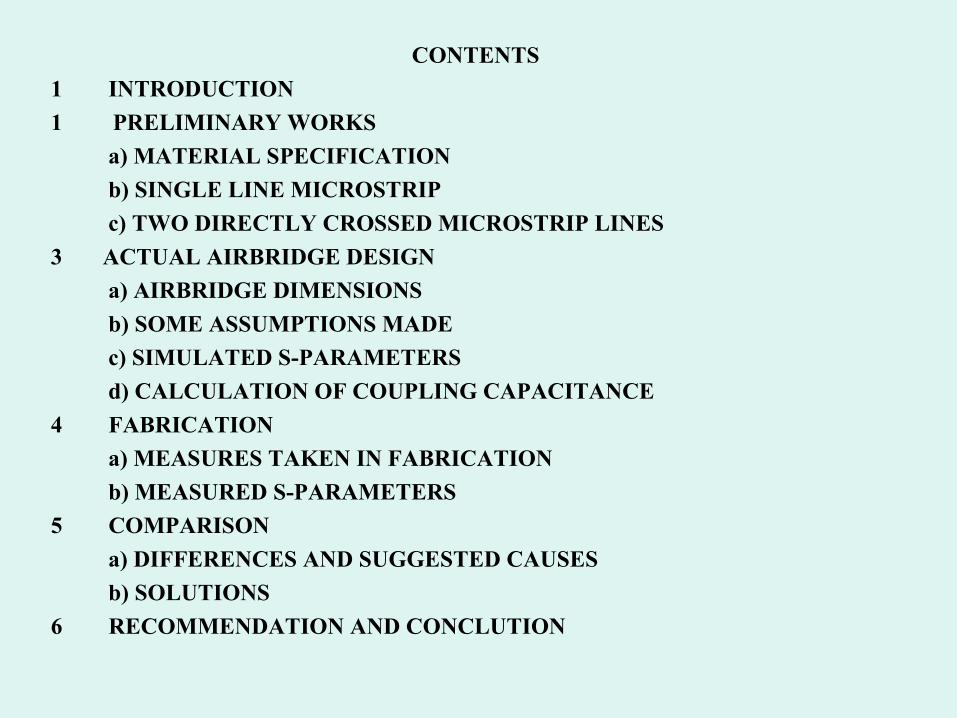
CONTENTS
1 INTRODUCTION
1 PRELIMINARY WORKS
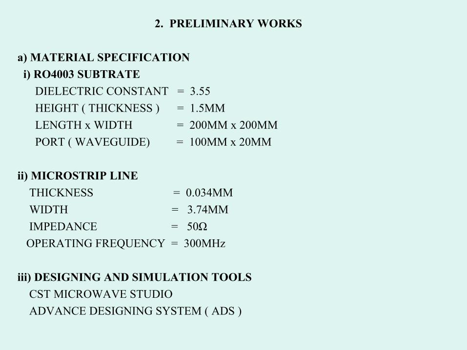
a) MATERIAL SPECIFICATION
b) SINGLE LINE MICROSTRIP
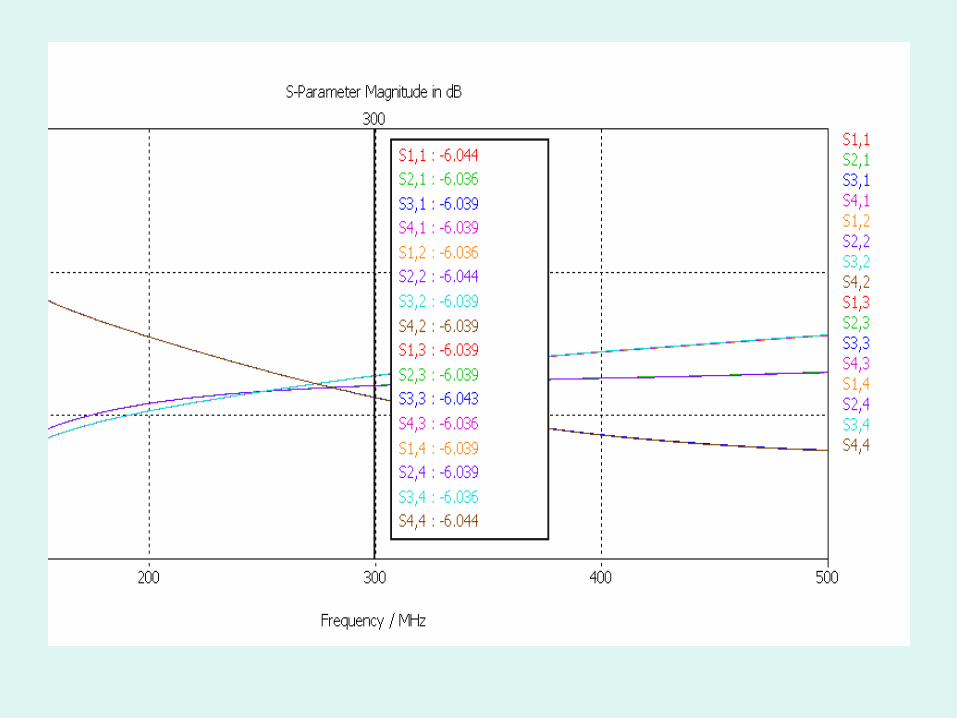
c) TWO DIRECTLY CROSSED MICROSTRIP LINES
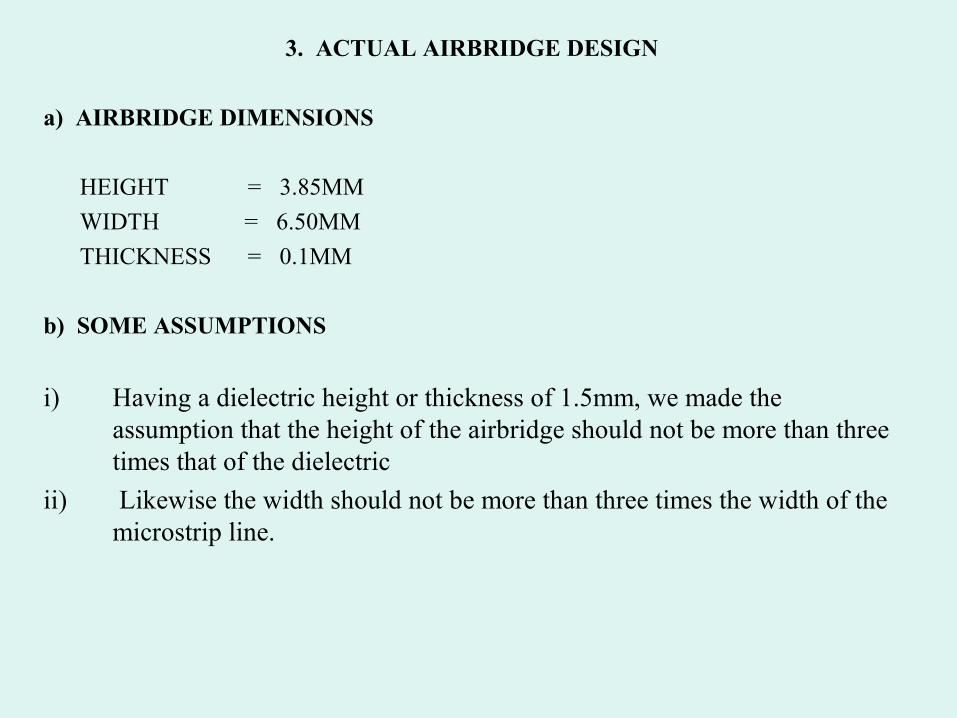
3 ACTUAL AIRBRIDGE DESIGN
a) AIRBRIDGE DIMENSIONS
b) SOME ASSUMPTIONS MADE
c) SIMULATED S-PARAMETERS
d) CALCULATION OF COUPLING CAPACITANCE
4 FABRICATION
a) MEASURES TAKEN IN FABRICATION
b) MEASURED S-PARAMETERS
5 COMPARISON
a) DIFFERENCES AND SUGGESTED CAUSES
b) SOLUTIONS
6 RECOMMENDATION AND CONCLUTION
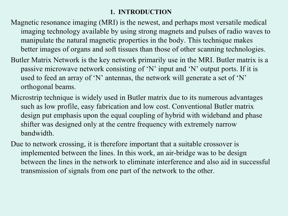
1. INTRODUCTION
Magnetic resonance imaging (MRI) is the newest, and perhaps most versatile medical imaging technology available by using strong magnets and pulses of radio waves to manipulate the natural magnetic properties in the body. This technique makes better images of organs and soft tissues than those of other scanning technologies.
Butler Matrix Network is the key network primarily use in the MRI. Butler matrix is a passive microwave network consisting of ‘N’ input and ‘N’ output ports. If it is used to feed an array of ‘N’ antennas, the network will generate a set of ‘N’ orthogonal beams.
Microstrip technique is widely used in Butler matrix due to its numerous advantages such as low profile, easy fabrication and low cost. Conventional Butler matrix design put emphasis upon the equal coupling of hybrid with wideband and phase shifter was designed only at the centre frequency with extremely narrow bandwidth.
Due to network crossing, it is therefore important that a suitable crossover is implemented between the lines. In this work, an air-bridge was to be design between the lines in the network to eliminate interference and also aid in successful transmission of signals from one part of the network to the other.
2. PRELIMINARY WORKS
a) MATERIAL SPECIFICATION
i) RO4003 SUBTRATE
DIELECTRIC CONSTANT = 3.55
HEIGHT ( THICKNESS ) = 1.5MM
LENGTH x WIDTH = 200MM x 200MM
PORT ( WAVEGUIDE) = 100MM x 20MM
ii) MICROSTRIP LINE
THICKNESS = 0.034MM
WIDTH = 3.74MM
IMPEDANCE = 50Ω
OPERATING FREQUENCY = 300MHz
iii) DESIGNING AND SIMULATION TOOLS
CST MICROWAVE STUDIO
ADVANCE DESIGNING SYSTEM ( ADS )
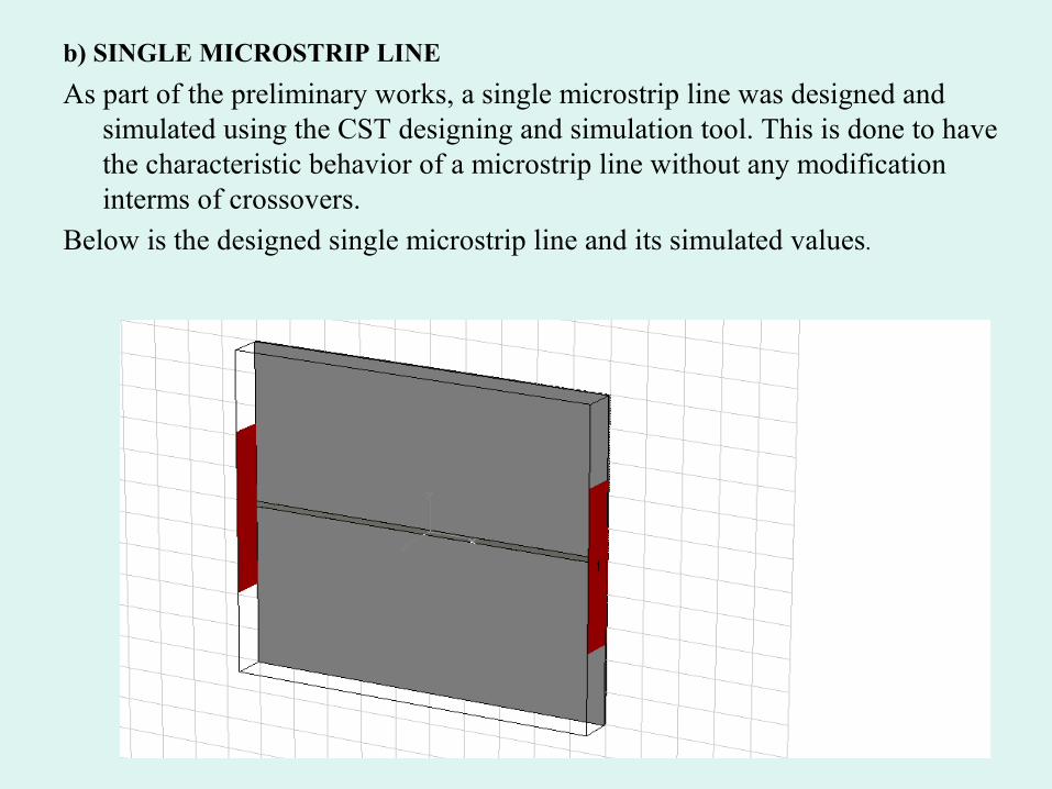
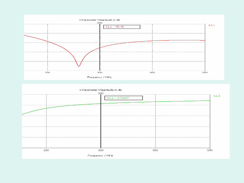
b) SINGLE MICROSTRIP LINE
As part of the preliminary works, a single microstrip line was designed and simulated using the CST designing and simulation tool. This is done to have the characteristic behavior of a microstrip line without any modification interms of crossovers.
Below is the designed single microstrip line and its simulated values.
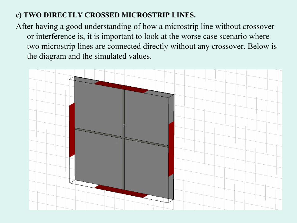
c) TWO DIRECTLY CROSSED MICROSTRIP LINES.
After having a good understanding of how a microstrip line without crossover or interference is, it is important to look at the worse case scenario where two microstrip lines are connected directly without any crossover. Below is the diagram and the simulated values.
3. ACTUAL AIRBRIDGE DESIGN
a) AIRBRIDGE DIMENSIONS
HEIGHT = 3.85MM
WIDTH = 6.50MM
THICKNESS = 0.1MM
b) SOME ASSUMPTIONS
i) Having a dielectric height or thickness of 1.5mm, we made the assumption that the height of the airbridge should not be more than three times that of the dielectric
ii) Likewise the width should not be more than three times the width of the microstrip line.
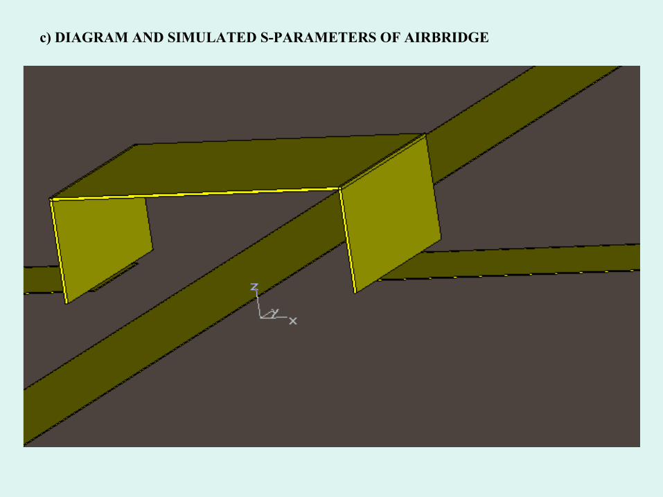
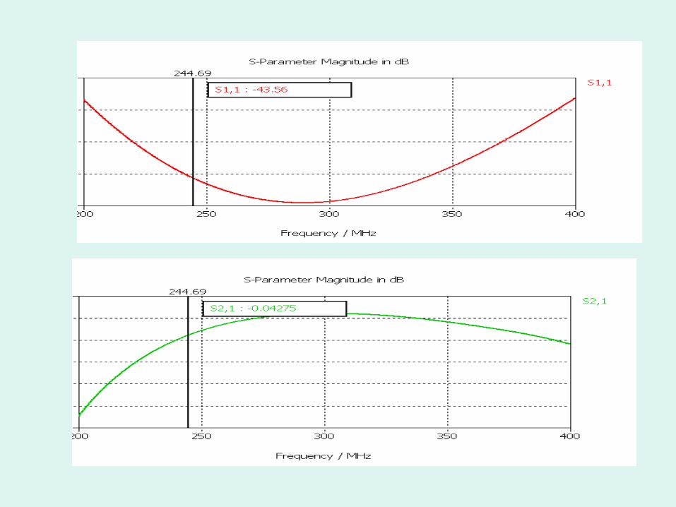
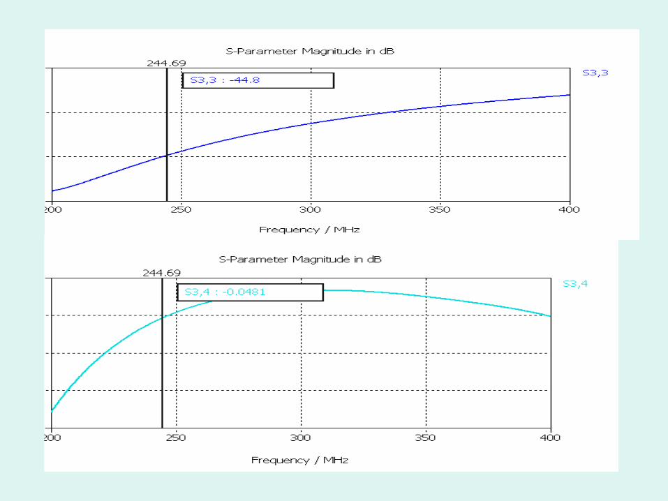
c) DIAGRAM AND SIMULATED S-PARAMETERS OF AIRBRIDGE
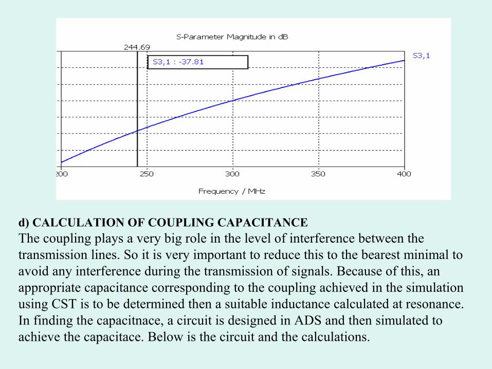
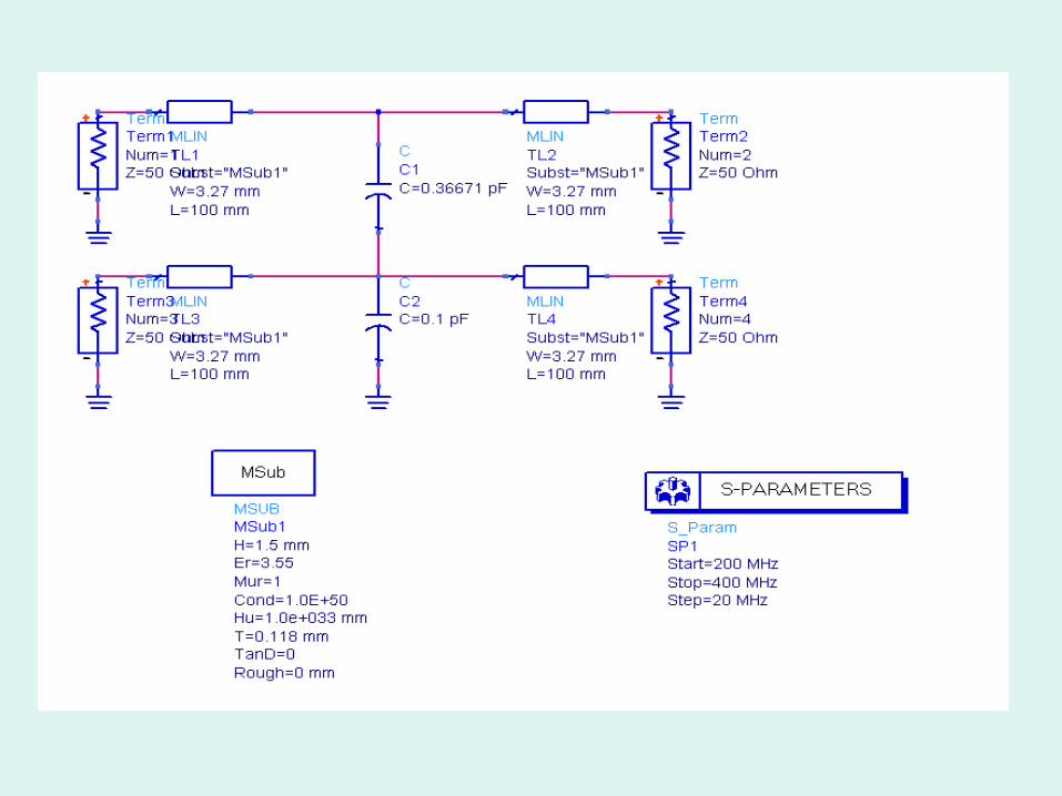
d) CALCULATION OF COUPLING CAPACITANCEThe coupling plays a very big role in the level of interference between the transmission lines. So it is very important to reduce this to the bearest minimal to avoid any interference during the transmission of signals. Because of this, an appropriate capacitance corresponding to the coupling achieved in the simulation using CST is to be determined then a suitable inductance calculated at resonance. In finding the capacitnace, a circuit is designed in ADS and then simulated to achieve the capacitace. Below is the circuit and the calculations.
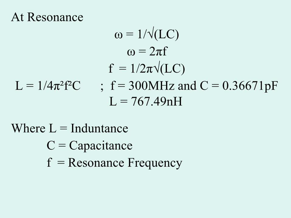
At Resonanceω = 1/√(LC)
ω = 2πff = 1/2π√(LC)
L = 1/4π²f²C ; f = 300MHz and C = 0.36671pFL = 767.49nH
Where L = Induntance C = Capacitance f = Resonance Frequency
4. FABRICATION
Fabrication of the designed airbridge is essential because it gives as how practical and accurate our designed was. In simple terms, fabrication gives us an insight to how best we can modify ( if the need be) of our designed work and the necessary improvements that should be done.
a) MEASURES TAKEN IN THE FABRICATION
i) Making sure the airbridge is moulded according the the designed dimensions and also approximating to two decimal places
ii) Also making sure the bubble in the copper material surface is reduce to a minimum.
iii) The soldering be done with care to avoid so much soldering material at points of soldering.
iv) Proper calibration of the Analyser before using for measurement
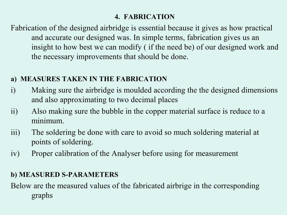
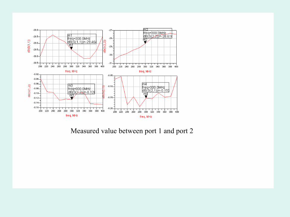
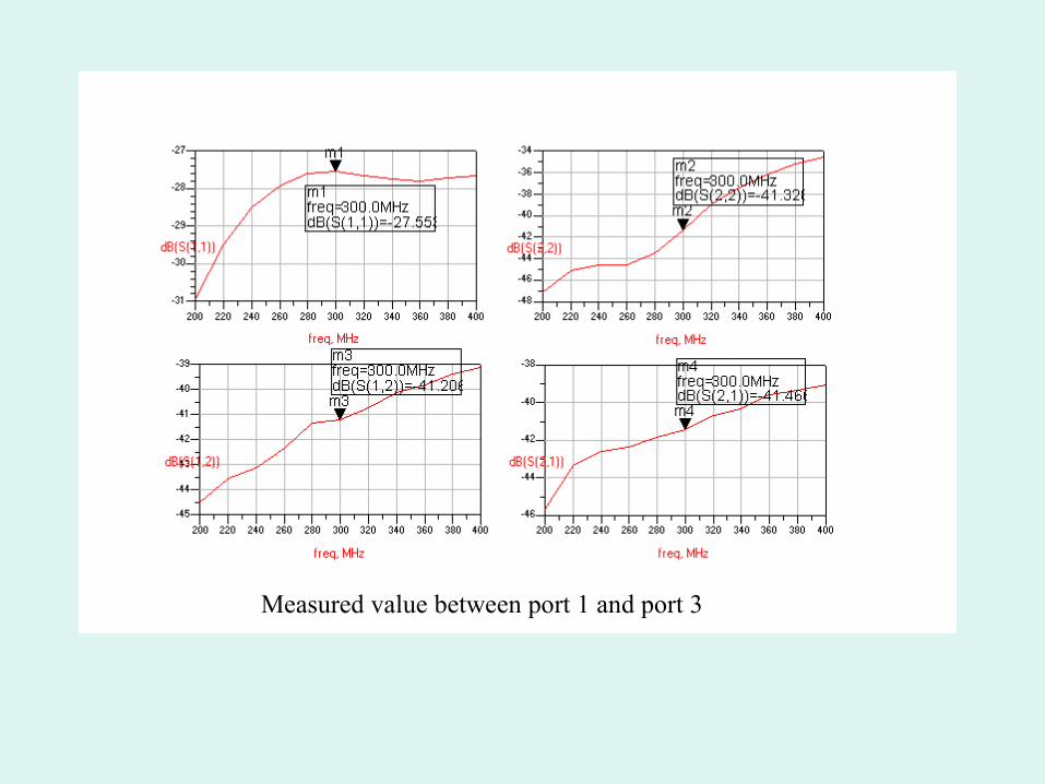
b) MEASURED S-PARAMETERS
Below are the measured values of the fabricated airbrige in the corresponding graphs
Measured value between port 1 and port 2
Measured value between port 1 and port 3
Measured value between port 1 and port 4
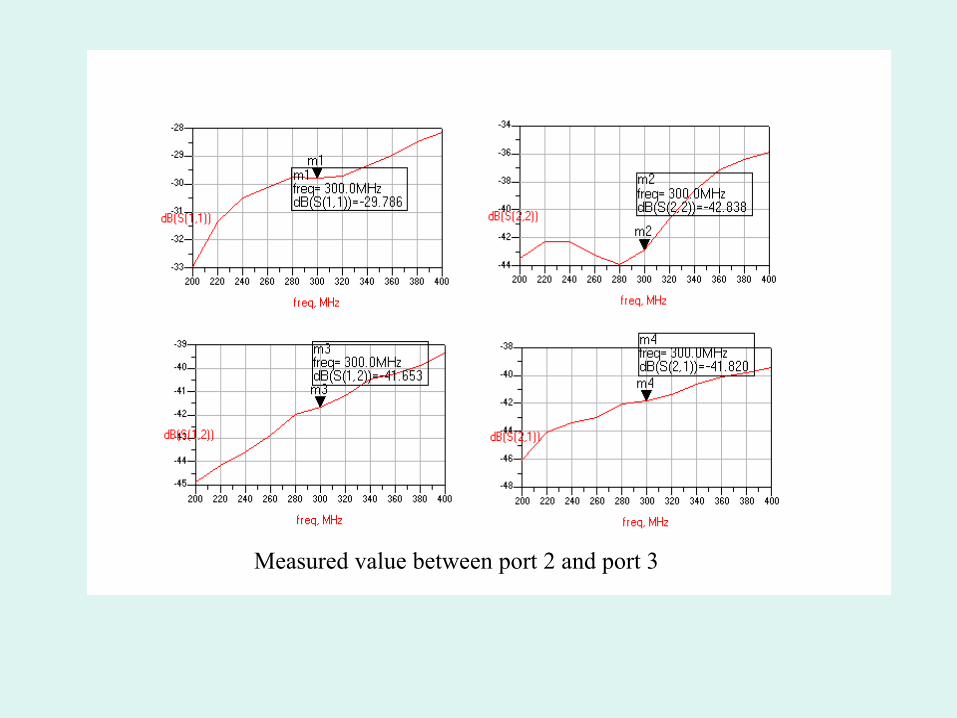
Measured value between port 2 and port 3
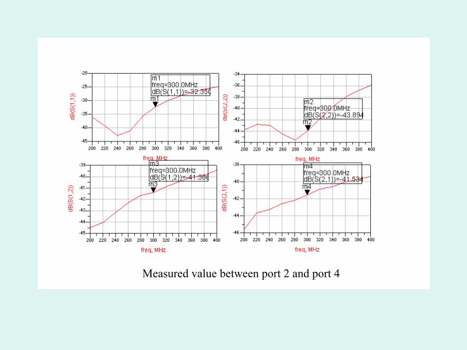
Measured value between port 2 and port 4
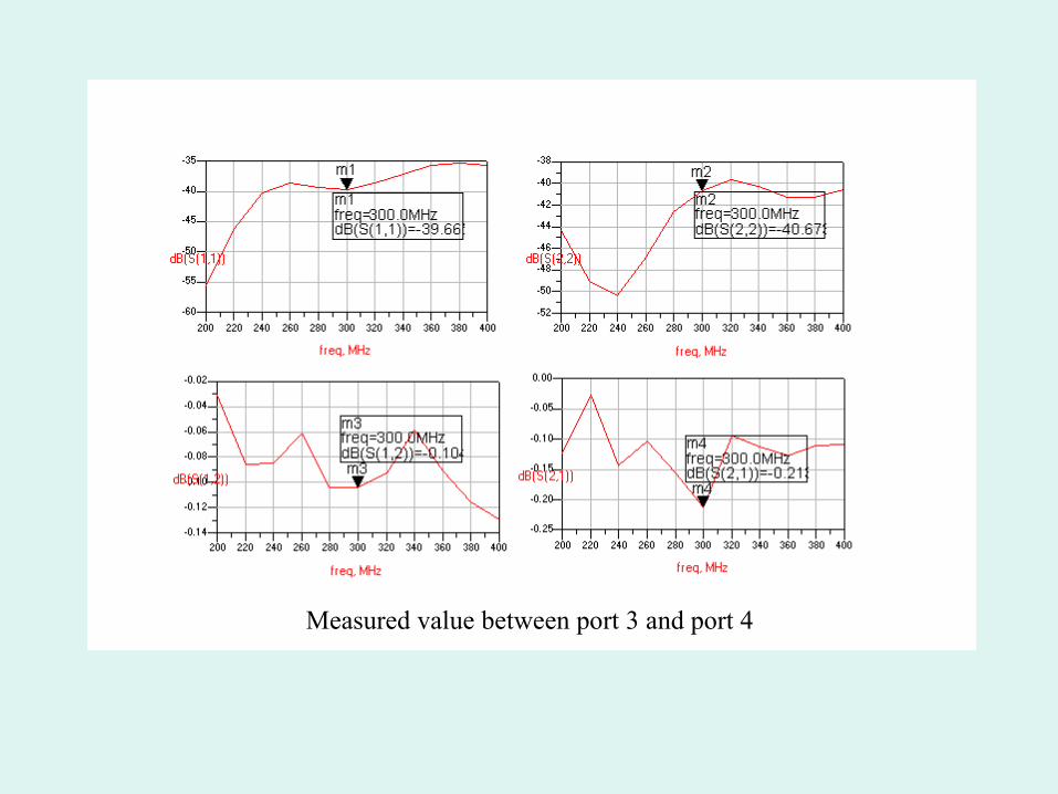
Measured value between port 3 and port 4
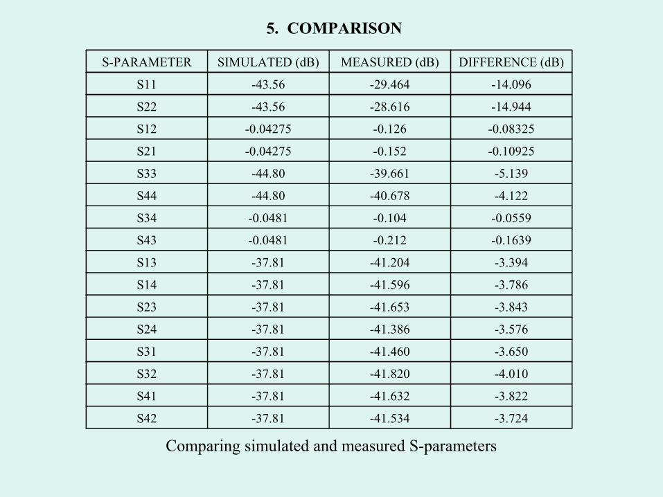
5. COMPARISON
S-PARAMETER SIMULATED (dB) MEASURED (dB) DIFFERENCE (dB)
S11 -43.56 -29.464 -14.096
S22 -43.56 -28.616 -14.944
S12 -0.04275 -0.126 -0.08325
S21 -0.04275 -0.152 -0.10925
S33 -44.80 -39.661 -5.139
S44 -44.80 -40.678 -4.122
S34 -0.0481 -0.104 -0.0559
S43 -0.0481 -0.212 -0.1639
S13 -37.81 -41.204 -3.394
S14 -37.81 -41.596 -3.786
S23 -37.81 -41.653 -3.843
S24 -37.81 -41.386 -3.576
S31 -37.81 -41.460 -3.650
S32 -37.81 -41.820 -4.010
S41 -37.81 -41.632 -3.822
S42 -37.81 -41.534 -3.724
Comparing simulated and measured S-parameters
a) DIFFERENCES AND SUGGESTED CAUSES
Comparing the simulated and measured S-parameters give us a good understanding of the task and the possible suggestions and recommendations that will be vital in further work on this topic.
DIFFERENCES
From the above Table, the most obvious difference in values occurred in the reflection coefficient between port 1 and port 2 where the air-bridge is located. As a matter of fact some difference is expected but -14dB between the simulated and measured value where the measured value for the air-bridge is just around -30dB raise some concern.
Another occurrence is the value of the measured value of the coupling which on an average is -41dB which is greater than the simulated value at -37.81dB is wealth looking at.
With this value of coupling which is so small, it follows that it will not be necessary improving or enhancing it at resonance with a suitable inductor.
Now our main task is to find the reason for such difference in the reflection coefficient and the best way to improve upon
SUGGESTED CAUSES
• One crucial area that was identified after looking again at the designing procedure is the size of the port. I realized that a slight change in the length or height of the port size causes a great change in value of the simulated values. According to CST tutorials, the port length should be at least 6-10 times the width of the transmission line but suggested a longer port length is better
• The other possible identified cause was the size of the PCB board which in my work was 200mm x 200mm which was just too big. The difficulty came to light when taking the measurements with the Network Analyzer. It was so difficult connecting the ports of the Analyzer and also maintaining the board on a level and stable status and I believe it did affected the measurement.
b) SOLUTION TO THE DIFFERENCE IN MY TASK
Instead of using a suitable inductor to enhance the coupling, looking at the measured values and as stated earlier wouldn’t be that necessary because the coupling is so small to avoid the interference between the transmission lines. What we need to look at now is improving the reflection coefficient between port 1 and port 2. In microwave transmission, one technique that is employ is the use of a STUB.
Stubs are shorted or open circuit lengths of transmission line which produce a pure reactance at the attachment point. Any value of reactance can be made, as the stub length is varied from zero to half a wavelength. A stub consists of a side section of line attached in series with (or in shunt with) the main transmission line, at a point to be determined. The length of the line, and the point of attachment, both need to be calculated from the load impedance. The stub needs to be nearly lossless; it may be open circuit, or short circuit, or indeed terminated in a pure reactance.
6. RECOMMENDATION AND CONCLUSION
RECOMMENDATION
• From my work on this task, I realised that careful planning is crucial in a good design especially when it comes to dimensions. I will recommend that a good size PCB board be use in further work on this task of 3cm (square) – 5cm (square) for ease and good stability in measurement. I also recommend a critical look at the ports size be done to select a good size. In this task, a waveguide type of port was used; I suggest a discrete port be also use in further works.
• One other form of design that I came across during my work on this task is the use of PADS at the foot of the air-bridge. This Pads act as some form of capacitors to reduce the high impedance cause by the air-bridge. It is a very interesting technique in air-bridge design and I suggest it should be look at in further works.
CONCLUSION
• Concluding, I will say the simulated and measured values confirmed that this design of air-bridge is very practical and applicable in High Frequency Networks. This work has set a good background upon which other works relating to this task can be carried out so as to achieve a very comprehensive air-bridge design either by the use of suitable inductor to enhance the coupling, a stub to reduce the reflection coefficient or the use of pads

THANK YOU VERY MUCH FOR LISTENING