Embed Size (px)
Citation preview
Preparation/Characterization of Atomically Flat and Clean Mo(100) Surfaces and Thermal Emittance/Response Time
Measurements of Cs3Sb Photocathodes
Matthew A. NicholsDepartments of Physics and Mathematics,
University of California, Berkeley, Berkeley, CA 94720
(Dated: August 12, 2011)
CsK2Sb photocathodes have recently proven to be a useful alternative to GaAs
photocathodes for the electron DC gun of the newly designed Energy Recovery Linear
accelerator at Cornell University due to their high quantum efficiency with visible
radiation and their expected longer lifetimes. The multi-alkali photocathodes grown
for the ERL injector have shown QEs that are a factor of 2 lower than values reported
by other sources. The major aims of this project is to build a vacuum chamber
designed for the purpose of LEED/AES analysis and preparation of Mo substrates
and to explore the effect of the Mo (100) surfaces prepared in this system on the
quantum efficiency/spectral response of CsK2Sb photocathodes. A second purpose is
to grow Cs3Sb photocathodes on Si (100) substrates, obtain quantum efficiency maps
of the cathodes, and measure, for the first time, the thermal emittances and response
times of the cathodes in the ERL injector itself. At the completion of this project,
it was found that the Mo substrates may have improved the spectral performance
of the multi-alkali photocathodes (by a factor of 2 in the green) and that the Cs3Sb
photocathodes had thermal emittance values and response times nearly identical to
those of the CsK2Sb photocathodes recently measured in the ERL injector.
2
I. INTRODUCTION
The Energy Recovery Linac (ERL) is a newly proposed linear accelerator at Cornell Uni-versity that is designed to produce some of the brightest X-rays ever generated by an X-raylight source facility. These X-rays require an electron beam with a very high brightness,where the beam’s brightness is defined as the ratio of the beam’s current to the beam’semittance[2]. The hope is that the ERL will be able to operate at a high average cur-rent of about 100 mA while maintaining a small six-dimensional phase space during beamacceleration[1]. In order to achieve this goal, the ERL will make use of a DC electron injec-tor which operates on laser based photoemission of electrons. This injector should produceelectron bunches that are around 2 ps in pulse duration.
Ultimately the brightness of the electron beam in the ERL will depend on the brightnessof the beam produced directly by the photocathode used in the injector. The brightnessproduced by the photocathode depends of course on the various intrinsic properties of thecathode itself. Achieving such a high brightness requires cathodes which have a short re-sponse time, low thermal emittance, and a long lifetime (practically speaking). Additionally,these photocathodes must have a high quantum efficiency within the visible portion of theelectromagnetic spectrum because achieving such a high average current requires an ex-tremely powerful laser and powerful lasers are most easily made in the visible wavelengths.
GaAs photocathodes have been the primary cathode used in the prototype injector upuntil this point. These cathodes have demonstrated both high QE in the visible as well as lowthermal emittance. One of the major issues with the GaAs photocathodes is that they have ashort operational lifetime: on the order of a few hours. These cathodes require vacuum levelson the order of 10−11 Torr in order to remain active, and for this reason an inter-vacuumsystem transport of these photocathodes has yet to be attempted at Cornell. Recentlyhowever, a new type of photocathode has been tested in the ERL injector: a bi-alkaliantimonide photocathode, CsK2Sb. These photocathodes are known to have sufficientlyhigh QE’s in the visible and are expected to have a much longer lifetime than GaAs: on theorder of days. The bi-alkali cathodes grown at Cornell however have shown QE’s which area factor of 2 lower than those reported by other sources.
The main purpose behind this project is to explore a possible explanation for this unex-pected phenomenon: it may be possible that the Si (100) substrates on which the photocath-odes were grown have a mal-effect on the performance of the cathode due to the mismatchof the crystalline lattice parameters between Si and CsK2Sb. The Si substrates were goodto work with because they were cheap, easy to prepare, and had a relatively low RMS sur-face roughness. This project attempts to explore the benefits of using a different type ofsubstrate, molybdenum (100), whose lattice parameters are a better match with those ofCsK2Sb.
Most of the effort of this project was geared towards preparing the vacuum system thatwill be used in the future to prepare these Mo substrates for photocathode deposition andto carry out a proof-of-principle experiment. The preparation of these substrates involvesmechanical polishing, ion sputtering of the surface, and thermal annealing, and requiressurface analytic techniques such as Low-Energy Electron Diffraction (LEED) and AugerElectron Spectroscopy (AES) to monitor the surface conditions. Due to several experimentalsetbacks, a significant portion of the time spent on this project was geared towards fixingthe substrate preparation chamber and, more specifically, attempting to fix the LEED opticssystem (rather than moving on to the analysis of the substrate preparation and its effects).

3
There was enough time however, once the vacuum system had been built, to prepare twoMo substrates and test the effect these substrates had on the photoemissive properties ofthe CsK2Sb photocathode.
A small portion of this project was also spent measuring the quantum efficiency, thermalemittance, and response time of a Cs3Sb photocathode as a function of the incident photonwavelength. These three properties of this cathode have not previously been accuratelymeasured, and so the knowledge of the performance of this cathode compared to the bi-alkaliCsK2Sb cathode was desired. This cathode was grown in the same deposition chamber as thebi-alkali cathode and was used in the ERL injector prototype to measure these properties.
II. EFFECT OF MO SUBSTRATES ON THE QUANTUM EFFICIENCY OF
CSK2SB PHOTOCATHODES
A. Background
1. Photocathode Properties and Materials
The intrinsic properties of the photocathode are relevant for the purposes of the ERLbecause the brightness of the electron beam in the accelerator is ultimately limited bythe brightness of the electron beam emitted directly by the cathode, which depends onthe cathode’s properties. The properties which are most relevant for our purposes are thequantum efficiency (QE) and spectral response, the response time, the thermal emittanceand mean transverse energy, and the lifetime of the photocathode.
Quantum Efficiency: Defined as the number of electrons per incident photon, the quan-
tum efficiency (QE) is given by the formula QE = hνeIP
where I is the current emitted by thecathode and P is the laser power incident on the cathode. The spectral response is simplya measure of the quantum efficiency as a function of the incident photon wavelength (at aconstant power).
[2]Response Time: Defined as the time required for electrons excited by the incomingphotons to escape from the surface of the cathode. The response time for a given cathode ismeasured in the ERL injector using a deflector cavity to deflect an incident electron bunchin such a way that the bunch’s longitudinal profile (along the direction of propagation) isflipped vertically so it can be viewed with a detector.
[1]Thermal Emittance: Defined as the intrinsic emittance of the photocathode (i.e. theemittance of the beam emitted directly by the cathode). The normalized rms thermalemittance of an electron beam in a direction transverse to the direction of propagation is
given by εn,x= σx√
kBT⊥mec2
where σx is the rms laser spot size on the cathode, and kBT⊥ is the
transverse thermal energy of the cathode. The mean transverse energy is just as it sounds:it is the average energy of the electrons in the transverse directions and is related to themean transverse velocity spread of the beam. The normalized thermal emittance, given in
terms of the cathodes work function, is εn,x= σx√
hω−φeff3mec2
where φeff is the effective workfunction of the cathode.
Lifetime: Defined as the amount of time it takes for the QE of the cathode to drop to 1e
times its initial value. The lifetime is influenced both by the material of the cathode (e.g.semiconductor vs. metal) and the conditions of the vacuum/chamber the cathode sits induring gun operation. For example, GaAs (a semiconductor cathode) requires extremely

4
low vacuum levels (10−11 Torr) for a lifetime of only a few hours whereas a metal cathodelike copper can operate for months with a vacuum level of only 10−9 Torr.
There are two main classes of photocathodes: metals and semiconductors. Prime exam-ples of metal photocathodes include Cu, Mg, and Pb. Metal photocathodes are generallycharacterized by low quantum efficiencies (less than 0.1%) and the requirement of highenergy UV radiation to operate due to their large work function values. The metal photo-cathodes do have the advantage however of being very robust (i.e. insensitive to damage),having a long operational lifetime (depending on both the vacuum level and the procedureused to clean the surface), and a less stringent requirement on the vacuum level.
Examples of semiconductor cathodes include GaAs, CsK2Sb, and Cs3Sb. These cathodescan be broken up into two subcategories: positive electron affinity (PEA) cathodes andnegative electron affinity (NEA) cathodes, depending on whether the potential energy of thevacuum lies above or below the conduction band minimum of the cathode[2]. Semiconductingcathodes are generally characterized by higher quantum efficiencies (greater than 5%) andcan operate in the visible region of the electromagnetic spectrum. These types of cathodesgenerally require ultra high vacuum (10−10 Torr or better) because of their strong chemicalreactivity. This chemical reactivity is also responsible for their shorter operational lifetimes(compared to metal cathodes) which are typically on the order of days or even hours.
Due to the fact that the most powerful lasers are usually found in the visible region ofthe spectrum, and that the ERL requires a large average current (which demands a highQE from the photocathodes), the ERL injector makes use of semiconducting photocathodes.The two main cathodes used in the injector are CsK2Sb and GaAs, which are PEA and NEAcathodes respectively. GaAs has proven to be quite a successful cathode, having QE’s of upto 15% in the green, response times on the order of 2 ps, and low thermal emittance values.However, GaAs cathodes require vacuum levels of 10−11 Torr in order to survive the amountof time sufficient for operation. This increased sensitivity to the vacuum level is due to theactivating Cs monolayer used on most GaAs photocathodes: this Cs is highly reactive withoxygen and is easily swept away, limiting the lifetime of these cathodes to days or even hours.CsK2Sb photocathodes on the other hand, while maintaining high QEs in the green (around10-12%) and short response times, have a much longer operational lifetime (on the orderof days). The difference in lifetime is the main reason we would like to switch to CsK2Sbfrom GaAs cathodes: having to swap out photocathodes every few hours (which means thewhole facility will be non-operational during the time needed to replace the puck) is not arealistic idea for an X-ray user facility like the ERL. Thus, we are very interested in learningas much as possible about these bi-alkali photocathodes and their various properties.
2. Substrate-Photocathode Film Interface
The quantum efficiency of a photocathode depends heavily on the mean free path of theexcited electrons in the bulk of the cathode material. If the mean free path of the excitedelectrons is too short, the electrons will not be able to travel very far before suffering ascattering event. These collisions cause the electrons to lose part of their energy, and ifenough energy is lost, they will not have enough left to make it above the potential barrierat the surface of the cathode. A longer mean free path means the electrons can maintaintheir energy for longer distances, and thus have more of a chance of escaping from thecathode surface and contributing to the cathode’s quantum efficiency.
Defects within the semiconductor material itself can act as recombination centers. This
5
means that a higher defect density leads to a shorter mean free path (MFP) for the excitedelectrons. Thus, in order to improve the electron MFP, and thus the QE of the cathode, ithelps to reduce the density of these crystalline defects. One possible cause of these defectsis the interface between the substrate and the photocathode film. Mismatch between thecrystalline structures (e.g. lattice parameters and unit cell shape) of the substrate andcathode film can cause strain within the cathode crystal, which may lead to crystallinedefects (line defects, plane defects, etc). By using a substrate which minimizes the mismatchbetween the two crystal structures, it may be possible to limit the number of defects withinthe cathode crystal, thus improving the cathode’s quantum efficiency.
The reason molybdenum was chosen as a possible substitute for the Si (100) substratesused in the past is that Mo (100) could possibly reduce the lattice mismatch with the cathodecrystal to as low as 3%. This is because the lattice parameters of the CsK2Sb cathode andMo (100) crystals are 8.61A and 3.14A respectively , and a 45 degree rotation of the Mo (100)crystal with respect to the cathode unit cell places the lattice constant of the cathode within3% of an integer multiple (namely 2) of the lattice constant of Mo (100). This improvedmismatch should lower the defect density and improve the cathode QE compared to thevalues measured using the Si (100) substrates.
In order to prepare the Mo (100) substrates for cathode deposition, the roughness ofthe surface must be greatly improved: hours of mechanical polishing and the use of a 100nm particle size diamond suspension helps reduce the RMS roughness of the surface to thedesired value of 10’s of nanometers (with improvements in the process needed in order toreduce the number of large scale defects). In order to improve the grain size of the Mo(100) crystals, a thermal annealing process is employed which may also improve the surfaceroughness. An increased grain size helps to decrease the strain on the CsK2Sb crystal since itwill reduce the number of crystalline interfaces between the different Mo crystalline domainsand the CsK2Sb crystal, which reduces the strain on the CsK2Sb crystal. In order to improvethe annealing process, an ion sputtering of the surface is employed which removes severalsurface layers and creates a sort of clean slate for the annealing to perform its duty.
3. LEED
Low-Energy Electron Diffraction is an experimental method used to analyze the twodimensional structural properties of crystalline surfaces. A typical LEED optics systemconsists of an electron gun, 4 energy selecting grids, a phosphorescent screen to display theelectron diffraction pattern, and a grounded crystalline sample. The energy of the electronsleaving the gun can be varied and typically ranges from 0-1500 eV. The current of theincident electrons can also be varied using the LEED electronics controller, but for thepurposes of this project, currents no higher than about 2 mA were used.
After leaving the gun and striking the sample, the electrons bounce back and pass throughthe series of 4 grids. The first grid is usually grounded to isolate the sample and the electronsin the vicinity of the sample from the voltages of the other grids. The second and thirdgrids are set to a negative potential in order to act as a sort of high pass filter for thereturning electrons. That is, when the electrons strike the sample surface, they can eitherundergo elastic scattering from the surface, or inelastic scattering within the crystal. Theelastically scattered electrons are the only ones which undergo diffraction, and so these arethe only electrons worth keeping around. Since these electrons have higher energy than onesthat undergo inelastic scattering (since the latter lose part of their energy to the inelastic
6
collision), it is possible to eliminate the other electrons by using a sort of high pass energyfilter.
By placing a conducting grid set to a negative potential in the electron beam path, onlythose electrons with enough energy to overcome the potential barrier can pass through thegrid, leaving only the elastically scattered electrons. The second and third grids, calledthe selector grids, are maintained at the same potential (by connecting them with a wire)because the two grids together form a more stable high pass filter than a single grid alone.The fourth grid is grounded to isolate the selector grid voltages from the voltages of thescreen. The screen is set to a high positive potential (∼4 kV) to give the filtered electronbeam enough energy to make a significant trace on the phosphorescent screen.
Information about the actual structure of the surface (i.e. crystalline structure, latticeparameters, etc...) is obtained using the diffraction pattern that LEED produces. Becausethe electrons are of such low energy, this diffraction pattern is extremely sensitive to theconditions of the surface (especially the first ∼4 monolayers). For example, surface con-taminants or extra rough surfaces can completely wash out the diffraction pattern. For thisreason, the crystal surface needs to be kept as clean and flat as possible (obtained throughpolishing of the surface or by using a freshly cleaved crystal). One way to do this is bykeeping the sample under ultra high vacuum: once the surface is cleaned and ready, vacuumlevels on the order of 10−10 Torr provide at least 2-3 hours of time to analyze the surfacewith LEED before enough residual gases in the chamber have adsorbed to the surface towash out the diffraction pattern. For a vacuum level of about 10−9 Torr, this time is reducedto about 20 or 30 minutes.
For the purposes of this particular project, the only aspect of the diffraction patternthat will be used will be the spatial configuration of the diffracted beams on the screen (asopposed to the spot intensities). This is because, for our purposes, LEED will mostly beused as a sort of binary test of the cleanliness and well-ordered structure of the crystal.Because LEED is so sensitive to the condition of the surface, a lack of a LEED pattern froma crystalline surface acts as an indication that the surface is either not clean enough, notflat enough, or not well-ordered. This is an extremely useful indication for the purposes ofthis project because we would like to know whether or not the Mo substrates (prepared viamechanical polishing, ion sputtering, and annealing) are sufficiently clean, flat, and well-ordered for the purposes of the photocathode deposition. We want to test the effect of theMo (100) crystalline planes on the photocathode’s photoemissive properties, and so we needto know whether these planes have been prepared well enough to suit this purpose.
The spatial configuration of the diffracted beams (i.e. the locations of the spots onthe screen) can be used to determine information about the 2-D unit cell which forms thesurface of the crystal. The basic diffraction condition is determined by the conservation
of momentum parallel to the crystalline surface, and is given by ~kr‖ = ~ki‖ + ~g where ~g =
h1~a∗ + h2
~b∗, ~a∗ and ~b∗ are the reciprocal lattice vectors of the crystalline surface unit cell
formed by the vectors ~a and ~b, and ~kr‖,~ki‖ denote the components of the reflected and incident
electron wave vectors parallel to the surface. The reciprocal lattice vectors are related to the
vectors forming the surface 2-D unit cell by the equations ~a∗= 2π(
~b×~n~a·(~b×~n)
), ~b∗= 2π
(~n×~a
~b·(~n×~a)
)where ~n is a vector normal to the crystal surface. Using these equations, it is possible to takea given diffraction pattern, examine the locations of the diffracted electron beams on thescreen, and determine the unit cell shape and lattice parameters of the surface. This willbe useful for mapping out the various crystalline domains of the Mo samples (something
7
beyond the scope of this project, but which is necessary in the future), which is used todetermine the makeup of the Mo substrates that have been prepared.
B. Experimental Methods
1. Experimental Setup
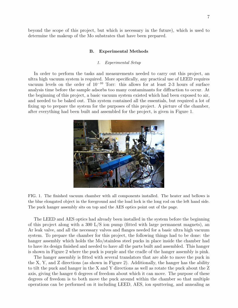
In order to perform the tasks and measurements needed to carry out this project, anultra high vacuum system is required. More specifically, any practical use of LEED requiresvacuum levels on the order of 10−10 Torr: this allows for at least 2-3 hours of surfaceanalysis time before the sample adsorbs too many contaminants for diffraction to occur. Atthe beginning of this project, a basic vacuum system existed which had been exposed to air,and needed to be baked out. This system contained all the essentials, but required a lot offixing up to prepare the system for the purposes of this project. A picture of the chamber,after everything had been built and assembled for the project, is given in Figure 1.
FIG. 1. The finished vacuum chamber with all components installed. The heater and bellows is
the blue elongated object in the foreground and the load lock is the long rod on the left hand side.
The puck hanger assembly sits on top and the AES optics point out of the page.
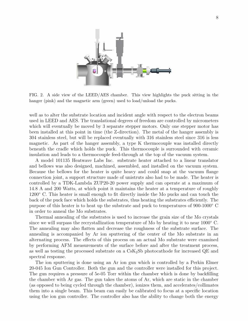
The LEED and AES optics had already been installed in the system before the beginningof this project along with a 300 L/S ion pump (fitted with large permanent magnets), anAr leak valve, and all the necessary valves and flanges needed for a basic ultra high vacuumsystem. To prepare the chamber for this project, the following things had to be done: thehanger assembly which holds the Mo/stainless steel pucks in place inside the chamber hadto have its design finished and needed to have all the parts built and assembled. This hangeris shown in Figure 2 where the puck is purple and the cradle of the hanger assembly is pink.
The hanger assembly is fitted with several translators that are able to move the puck inthe X, Y, and Z directions (as shown in Figure 2). Additionally, the hanger has the abilityto tilt the puck and hanger in the X and Y directions as well as rotate the puck about the Zaxis, giving the hanger 6 degrees of freedom about which it can move. The purpose of thesedegrees of freedom is to both move the puck around within the chamber so that multipleoperations can be performed on it including LEED, AES, ion sputtering, and annealing as
8
FIG. 2. A side view of the LEED/AES chamber. This view highlights the puck sitting in the
hanger (pink) and the magnetic arm (green) used to load/unload the pucks.
well as to alter the substrate location and incident angle with respect to the electron beamsused in LEED and AES. The translational degrees of freedom are controlled by micrometerswhich will eventually be moved by 3 separate stepper motors. Only one stepper motor hasbeen installed at this point in time (the Z-direction). The metal of the hanger assembly is304 stainless steel, but will be replaced eventually with 316 stainless steel since 316 is lessmagnetic. As part of the hanger assembly, a type K thermocouple was installed directlybeneath the cradle which holds the puck. This thermocouple is surrounded with ceramicinsulation and leads to a thermocouple feed-through at the top of the vacuum system.
A model 101135 Heatwave Labs Inc. substrate heater attached to a linear translatorand bellows was also designed, machined, assembled, and installed on the vacuum system.Because the bellows for the heater is quite heavy and could snap at the vacuum flangeconnection joint, a support structure made of unistruts also had to be made. The heater iscontrolled by a TDK-Lambda ZUP20-20 power supply and can operate at a maximum of14.8 A and 200 Watts, at which point it maintains the heater at a temperature of roughly1200◦ C. This heater is small enough to fit directly inside the Mo pucks and can touch theback of the puck face which holds the substrates, thus heating the substrates efficiently. Thepurpose of this heater is to heat up the substrate and puck to temperatures of 900-1000◦ Cin order to anneal the Mo substrates.
Thermal annealing of the substrates is used to increase the grain size of the Mo crystalssince we will surpass the recrystallization temperature of Mo by heating it to near 1000◦ C.The annealing may also flatten and decrease the roughness of the substrate surface. Theannealing is accompanied by Ar ion sputtering of the center of the Mo substrate in analternating process. The effects of this process on an actual Mo substrate were examinedby performing AFM measurements of the surface before and after the treatment process,as well as testing the processed substrate on a CsK2Sb photocathode for increased QE andspectral response.
The ion sputtering is done using an Ar ion gun which is controlled by a Perkin Elmer20-045 Ion Gun Controller. Both the gun and the controller were installed for this project.The gun requires a pressure of 5e-05 Torr within the chamber which is done by backfillingthe chamber with Ar gas. The gun takes the atoms of Ar, which are static in the chamber(as opposed to being cycled through the chamber), ionizes them, and accelerates/collimatesthem into a single beam. This beam can easily be calibrated to focus at a specific locationusing the ion gun controller. The controller also has the ability to change both the energy
9
of the incident ions as well as the emission current. For this project, the ion sputtering wasused along with the thermal annealing in a 3 stage cycle: one cycle consists of 20 minutes ofsputtering followed by 30 minutes of annealing at temperatures greater than or equal to 850◦
C. The sputtering is used to remove layers of surface material including both contaminantsand Mo. This helps provide a sort of clean slate for the thermal annealing to restructurethe surface and make it clean and flat with large grain size.
Because the system is designed to have pucks transferred in and out (in order to preparemultiple substrates and to use LEED/AES to analyze surface structures), the system willbe opened up to air fairly often . That means that water, carbon monoxide, carbon dioxide,and oxygen can accumulate in the chamber after each puck transfer. Rather than havingto bake part of the chamber after each transfer (a process which would take an entire day),we found it much more convenient to install a titanium sublimation pump (TSP) at thebottom of the chamber near the 300 L/S ion pump. The TSP essentially consists of threeTi filaments through which 40-50 A of current is run. The current causes the filament toheat up, releasing Ti into the chamber. This elemental titanium sticks to the walls of thechamber and, because it is highly reactive, residual gases like water and carbon monoxidehit the walls of the chamber, react with the titanium there, and stick. This pump of coursedoes not work well for the noble gases which will not react with Ti.
Once a puck transfer occurs, and the load lock (see Figure 2) is pumped down with aturbo and ion pump to about 1e-08 Torr, the gate valve connecting the load lock with themain chamber is opened, bringing the main chamber pressure up from 1e-10 Torr to between1e-09 and 1e-08 Torr. In order to pump back down to 1e-10 Torr, the TSP is flashed forabout 5 minutes at ∼46 A to remove any water and other residual gases. If this does notwork, the TSP is flashed two or three more times to achieve the desired pressure. Thisallows the system to achieve the necessary pressures for LEED without having to do a bakeout, and this makes things much simpler/faster.
Before this project began, there was no way to perform the actual puck transfer withoutbreaking the vacuum of the entire chamber, placing the puck in the hanger, and pumpingdown/baking the whole chamber again. In order to reduce the amount of time needed toperform such a transfer, a load lock mechanism was designed and installed. This is picturedclearly in Figure 2. The load lock essentially consists of a loading gate which opens up to airvia the twist of a small knob and closes tightly with an o-ring, a magnetic arm and lineartranslator whose tip sits just inside the loading gate, a 40 L/S ion pump, a gate valve whichconnects the load lock to the main chamber, and a valve which connects to the turbo pumpto pump out the load lock.
To change the pucks in the system, we first open the gate valve separating the load lockfrom the main chamber. The magnetic arm, a long rod with a locking mechanism at the tipthat fits inside the pucks and holds them in place, is then inserted into the main chamberusing the magnetic translator. It is subsequently inserted into the back of the puck which isto be removed and which sits inside the cradle of the hanger assembly. The magnetic armlocks into the back of the puck, and the cradle is lowered using the Z-axis stepper motorso that the puck can be removed without hitting the cradle itself. The puck/arm are thenfree to move out of the chamber and back into the load lock through the gate valve. Thegate valve is then shut and the load lock is vented with nitrogen gas to limit the amount ofair which can enter. Once the load lock reaches atmospheric pressure, the loading gate isopened, the old puck is removed from the translator arm tip, and the new puck is placedon the end of the arm. The chamber is then pumped down via turbo and ion pumps to a

10
vacuum level between 1e-08 Torr and 1e-07 Torr at which point the gate valve is openedagain and the puck is placed carefully inside the cradle.
The magnetic arm has also found some use acting as a rigid object on which crystalscan be cleaved by pushing the crystal tip against the arm until it shatters. As a matterof convenience, a cold cathode gauge was placed on the top of the load lock chamber tomonitor pressures during pumping periods and during the Ar backfills when the ion pumppressure gauge could not be used due to the higher pressures. The cold cathode gauge, atthis location, is too far from the LEED optics to distort the electron beam motion with themagnetic field it produces.
Several other pieces of equipment which were installed on the vacuum system throughoutthis project include a firewire camera which sits centered on the diffraction screen justoutside the LEED optics port, an SRS RGA which sits around the middle section of themain chamber for monitoring partial pressures, and an ensemble of view ports around thetop of the main chamber used to view the puck from multiple angles while aligning the puckin front of the various tools (the LEED electron gun, the AES electron gun, the ion gun,and the heater). A mount had to be designed and installed on the viewport of the LEEDdiffraction screen to hold the camera tightly in place while providing it with a perfect viewof the entire screen. In order to reduce the amount of background light and reflection inthe pictures taken by the camera, a large black cloth was wrapped about the camera andmount.
Once the system had been fixed up with all the new parts and tools, it needed to bebaked out to remove water and other gases which may have adsorbed to the chamber wallssince it had been exposed to air for a long period of time. Before the bake out, the turboand ion pumps were able to bring the main chamber down to a pressure of about 1e-08Torr. The chamber was then wrapped with heat tape and coated in a double/triple layer ofaluminum foil. The bake out procedure and the parameters used are depicted in Figure 3.
FIG. 3. The parameters of the bake out are: soak temperature= 150◦C, ramp time 1 = 8 hours,
soak time= 32 hours, ramp time 2 = 8 hours, and the starting and finishing temperatures were
both 20◦ C.
Note that a higher soak temperature was not used during the bake out because of thepermanent magnets from the ion pump at the bottom of the chamber. Higher temperaturescould possibly demagnetize the magnets and render them and the ion pump useless. After 48hours of baking and several days of pumping with the ion pumps, the vacuum level reached1.5e-10 Torr in the main chamber (as measured by the ion pump gauge on the 300 L/Spump). It should also be noted that throughout the remainder of this project, whenever themain chamber was opened to replace parts such as the hanger cradle or the LEED optics,

11
the chamber was heavily vented with nitrogen gas. This, along with the use of the titaniumsublimation pumps, prevented the need for a second bake out of the chamber. That is,similar pressures were achieved without having to bake the chamber a second time.
2. Experimental Issues
Several problems were encountered throughout the process of setting up the LEED/Augerchamber that may have led to the improper functioning of the LEED optics system. Thatis, upon testing the LEED system on several well-ordered, clean, and freshly cleaved crystals(including Si and GaAs crystals), diffraction patterns were obtained that did not resemblethe expected patterns. For example, from a typical clean crystal, one would expect a diffrac-tion pattern which consists of several intense, small spots which conform to the diffractioncondition of the reciprocal lattice of the crystal being analyzed (as discussed in the sectionon LEED). However, the diffraction patterns obtained with this system did not resembleseveral small intense spots. The diffraction patterns obtained resembled more of a tie-dyepattern which did not seem to conform to any clear diffraction condition. Additionally, thesepatterns changed significantly (in shape, size, and location on the screen) according to theenergy of the incident electrons. Sometimes, the diffraction pattern would even drift withtime. An example of such a diffraction pattern is given in Figure 4.
FIG. 4. Distorted diffraction pattern: the black shape in the center is the electron gun with the
gun filament glowing red in the center
The first of these effects (the dependence of the pattern on the incident electron energy)may be explained by residual magnetic fields existing within the vicinity of the sample, theelectron gun, and the selector grids. It is of course possible that there is something elsecausing the distorted diffraction pattern: continuity of the electrical connections betweengrids was double checked and the shorting of the grids was also tested for. However, thesetests produced nothing of interest and so magnetic fields are still the prime suspect. Indeed,upon testing LEED on a YAG screen placed over the Mo puck, it was found that theelectron beam incident upon the YAG screen deviated significantly from its expected positionwhenever the puck hanger was rotated slightly (bringing the poles of the hanger closerto/further from the electron beam).
12
This effect only happened however when one particular pole on the hanger was broughtclose to the beam: rotating the sample while the other pole was closer did not result insignificant deviations. When the first pole was brought close to the beam, and the samplewas rotated through a small angle, the location of the beam on the screen would movevertically a much greater distance than it should under normal operating conditions. Thisindicated that one of the poles was producing a magnetic field which was altering the pathof the beam when the pole was close by. The fact that the pattern is also energy dependentseems to back up this assumption since particles traveling with different energies are actedupon with a different force (depending on the energy) in the presence of a magnetic fieldwhich could cause a distortion of the beam.
In order to test for the presence of such fields within the chamber and on the LEEDoptics (using a Hall probe), and because nothing else seemed to be wrong with the systemitself, the LEED system was removed from the vacuum chamber. It was found that fieldson the order of 2-5 gauss were actually present on the LEED optics at the welding jointswhich connected the wires to the various grids of the optics. These fields tended to drop tozero however in the vicinity of the electron gun and where the electron beam would reside.Regardless, we attempted to remove these fields by degaussing the entire optics system. Thedegaussing did not seem to affect the field strength however since the fields were still presentafter each degaussing.
The Hall probe was also used to test the field inside the chamber itself: it was found that,as expected, the puck hanger produced significant magnetic fields on the order of severalgauss, and even ∼14 gauss at a certain point. The reason for such fields resides in the factthat 304 stainless steel was used to construct the hanger/cradle device, and 304 stainlesssteel is somewhat magnetic. Thus, the hanger will need to be rebuilt from 316 stainless steelwhich is less magnetic. Due to time limitations, there was not enough time within the spanof this project to replace the hanger/cradle with the new stainless steel. For this reason,an attempt was made to degauss the puck hanger/cradle by removing the hanger, takingit apart, and degaussing each piece independently. The screws on the assembly were alsoreplaced with non-magnetic screws. The effect of the degaussing did not seem to be toosignificant, as in the case of the LEED optics, since the fields still resided within the hanger.The best move to make next is to simply replace any parts in the chamber which may bemagnetic in order to eliminate any possible residual fields in the chamber. The ion pumpused on this chamber employs the use of several powerful permanent magnets, however upontesting the fields of these magnets at the location of the puck with a Hall probe, no fieldsabove the ambient field seemed to be present.
The residual magnetic fields are the prime suspect for the failure of the LEED optics,however the drifting of the diffraction pattern with time may be caused by the presence ofstray electric fields produced by the charging up of some items within the vicinity of theelectron beam. The most likely candidates are the ceramic tiles which electrically insulatethe grids from one another and the multiple view ports which were added to the vacuumchamber. These viewports, if not coated with a conducting material, can build up a signif-icant amount of charge which causes distortions of the beam/diffraction pattern. Both ofthese theories still need to be tested since the presence of a conductive coating on the viewports is unknown, and time limitations prevented the testing of the ceramic tiles.
It is interesting to note however that these oddly shaped diffraction patterns occur onlywhen a clean, well-ordered crystal is used as the sample. For example, if the beam were tohit an unpolished Mo surface (like the puck itself without a substrate), no pattern would

13
appear. This was confirmed when testing LEED on a cleaved Si crystal: while the LEEDpatterns still resembled the figure above, the titanium sublimation pumps were accidentallyturned on, coating the sample and contaminating it with chemical species which react to thetitanium. As soon as this occurred, the diffraction pattern disappeared and was not able tobe recovered. For this reason, it is still possible to use LEED for the desired purpose of abinary test for the preparation of the Mo substrate surfaces: if the surface is clean and well-ordered after the annealing and sputtering, a diffraction pattern should appear. Otherwise,the pattern will simply be washed out. This use of LEED is of course sub-optimal. It wouldbe preferable to fix LEED in order to obtain actual (non-binary) information regarding thestatus of the Mo surface, and to even create a sort of domain map of the Mo surface, butthe status of the LEED optics at this moment seems to be satisfactory enough to allow forthe Mo sample preparation.
3. Software to Control Devices and Save Data
During the operation of the LEED/Auger chamber, there are several key parameters thatwe want to monitor and several devices we would like to operate remotely with a computer.We would also like to do all of these things using one single LabVIEW program. The deviceswe would like to operate remotely include the power supply for the heater, the residual gasanalyzer (RGA, SRS model RGA200), and a fire-wire camera used to photograph/monitorthe LEED screen where the diffraction patterns occur. Most of the code needed to communi-cate with and operate the RGA and heater power supply was written in LabVIEW previouslyby Luca Cultrera for use on the deposition chamber (where the multi-alkali photocathodesare deposited). The code used to operate the heater power supply was essentially completeand simply needed to be integrated into the overall code which monitored the LEED/Augerchamber. This power supply code controls the amount of current the power supply outputsto the heater and monitors/displays the voltage across the heater, the current output bythe supply, and the total power output of the power supply. The RGA operating code onthe other hand needed some significant edits to comply with the needs of the LEED/Augerchamber.
Specifically, the SRS RGA code was previously used only to read out the mass spectrumof the residual gases in the deposition chamber, and to display and plot the partial pressuresof up to seven gases (specified by their masses) as a function of time. This code did not havethe ability to read out the total pressure in the chamber while displaying the partial pressuresand the mass spectrum at the same time. For the purposes of the LEED/Auger chamber,we would like to monitor the total pressure using the RGA because the only other methodof measuring the pressure at the current stage of development is a gauge built into the ionpump controller. The ion gauge must be calibrated according to the pumping rate of the ionpump, and this value is not known accurately so that the pressure reading is not necessarilyaccurate. A cold cathode gauge is not used inside the main part of the LEED/Auger chamberdue to the fact that the cold cathode gauge produces a strong magnetic field which couldhave a very negative effect on the LEED system. Measuring the total pressure with theRGA will provide a more objective picture of what the real pressure inside the chamber is.
In order to achieve this goal, a slightly round about method had to be implementeddue to the fact that the RGA is both unable to make a total pressure measurement withthe electron multiplier on, and unable to make two types of measurements (e.g. partialpressure/mass spectrum and total pressure) at the same time. The most practical way to

14
get a total pressure reading was to use the RGA to obtain partial pressure/mass spectrumdata, and to use this data to estimate the total pressure in the chamber. Because the massspectrum is essentially a plot of pressure versus mass1, all one essentially needs to do isintegrate over the entire mass spectrum (i.e. sum up the contributions to the pressure dueto each mass) to obtain the total pressure due to all of the gases in the chamber. However,due to the fact that the peaks in the mass spectrum are of a finite width, this integral wouldyield a value for the total pressure which would be much higher than the actual value. Thesolution to this problem was to approximate the integral by a finite sum: using the entiremass spectrum (a series of data points over a finite range), the maximum value of every7 sequential data points was taken (in order to obtain just the max value of a pressurepeak rather than values over the entire finite peak), and each of these maxima was summedtogether. This method was tested in the deposition chamber and checked against the readingof the cold cathode gauge (which is calibrated for use on nitrogen gas). The resulting totalpressure was found to be within a factor of 2 higher than the cold cathode gauge value. Thisaccuracy is satisfactory for use in the LEED/Auger chamber since an order of magnitudemeasurement is all that is necessary.
In addition to the ability to measure total pressure, another key feature of the RGA codethat was added was the capability of turning the electron multiplier (CEM) of the RGA onand off at will. This feature is necessary because the Ar ion sputtering procedure used toclean the Mo surfaces requires that the chamber be backfilled with Ar gas up to a vacuumlevel of 5e-05 Torr. The electron multiplier of the RGA is not capable of operating at such ahigh pressure and so must be turned off in order to remain in a functioning state. Rather thanturning off the RGA entirely, we would like to simply press a button to shut off the electronmultiplier during the sputtering process. This would allow the RGA to continue runningduring the procedure in order to produce total pressure and partial pressure measurements(though the accuracy of these measurements will decline significantly once the electronmultiplier is off). Then, when the sputtering process is over, the electron multiplier may beturned back on with another simple press of a button. This button has been implementedinto the code exactly as desired, so that the CEM can be turned off/on, and yet the RGAwill continue to acquire data.
The section of the LEED/Auger chamber LabVIEW code dedicated to operating the fire-wire camera had to be written from scratch, but is straight forward and has no outstandingor unexpected features except for two things that are worth discussing. First of all, itis possible in LabVIEW, when the code is running, to display the camera output on thescreen, and to edit the color scheme of this output. More specifically, while analyzing theLEED diffraction patterns, it was beneficial to use this feature to change the normal camerafeed (which is in black and white) to a “gradient” color scheme which makes less brightfeatures a deep red, brighter features orange, and the brightest features white. This madethe diffraction patterns more visible and clear to the user. However, the code which waswritten, which has the ability to save images from the camera to a specified folder, saves theoriginal images from the camera, which are still in black and white. This, while somewhatuseful, is not optimal since the colored pictures provide a clearer view of the diffractionpatterns. As of now, the only method which can save these colored images is to manuallyuse “print screen” and save the printed screen image.
1 Technically, the RGA plots pressure versus mass per unit charge. However, if we assume a single ionization
for each mass, then we can assume the pressure is a function of mass alone. For the purposes of this
application, this assumption has no mal-effects since we are going to sum up over every mass to charge
value anyway, thus obtaining the total pressure due to each species of gas, regardless of whether a gas’
contribution to the pressure comes from the fact that it can be ionized twice, once, or even both.

15
The second thing worth mentioning is the fact that LabVIEW does not allow for acontinuous video feed from the camera. Rather, a slight delay had to be implementedbetween frames so that the program could keep up with the camera output. Thus, theimage displayed on the screen updates according to this delay time. If the delay time is tooshort, the camera display in the program will go blank and will not output any images. Ifthe delay is too long, the display will update very slowly, and the lag between what happensat the actual diffraction screen and what one sees on the computer screen will be too great,meaning that some details of the diffraction pattern could be lost if time is a factor. Theoptimal delay time found to operate the camera code alone was about 255 ms. This delaytime was found to be too short however when the camera code was integrated into theoverall LEED/Auger code (since the overall code is larger and has several loops runningsimultaneously). Thus, the delay time in the LEED/Auger code had to be increased toroughly 800-900 ms to display the camera feed without going blank. This lag is suboptimalof course, but is satisfactory enough for the moment. In the future, if this code is everoptimized, the delay time should be decreased.
In addition to operating several devices, the LEED/Auger chamber LabVIEW programis used to monitor several key parameters within the chamber including the temperatureof the cradle which holds the Mo pucks (from which we can obtain the temperature of thepuck and Mo substrate based on our calibration of the thermocouples), the pressure withinthe chamber as measured by a cold cathode gauge, and the current which flows throughthe puck itself. These values are monitored using an analog signal from the outputs of thevarious devices, reading this analog signal using an analog to digital converter (ADC), anddisplaying the output of the ADC in LabVIEW.
In order to measure the temperature, the thermocouple attached to the puck cradle isconnected to an OMEGA model 650 thermocouple box which converts the thermocouplevoltage to an actual temperature, and outputs an analog signal based on this value. Theoutput voltage is converted back to a temperature value in LabVIEW using the equationT = V ∗ 103, where V is the analog voltage across the output terminals and T is thedesired temperature value. The pressure is measured with a cold cathode gauge in the mainchamber which has yet to be installed due to the fact that the magnetic field produced bythe gauge may affect the operation of LEED. The cold cathode gauge controller has a DB15 connector on the back which produces the desired analog output signal. The pressureis obtained by measuring the voltage across pins 11 and 12 of the DB 15 connector andconverting this voltage to a pressure with the equation P = 10V−11, where P is the pressureand V is the voltage across the pins. The current is to be measured using a Keithley Model485 piccoammeter which has an analog voltage output on the back and which has also notbeen installed due to time limitations and other experimental issues. This voltage across theoutput is converted to the current measured by the piccoammeter according to the formulaI = S∗V
−2where V is the voltage and S is the setting on the piccoammeter box converted into
amps (i.e. 200 µA, 20 µA, etc). For example, for a voltage output of -0.065 V measured on
the 200 µA scale, the current would be I = 200∗10−06∗(−0.065)−2
= 6.5µA.
Each of these voltages is read using the ADC, and converted in the LabVIEW program,using the above formulas, to the desired parameter readings. Several things must be men-tioned regarding these readings however: due to a strange situation regarding the groundingof the thermocouple with respect to the vacuum chamber and the grounding of the ADC, thevoltage across the terminals of the OMEGA box must be measured in the following manner:first, the voltage of the positive terminal of the output is measured with respect to the ADC

16
ground and the voltage of the negative terminal of the OMEGA output is measured withrespect to the ADC ground. Then, these two values are subtracted to obtain the voltageacross the terminals. Finally, these values are averaged to eliminate noise and obtain a morestable measurement. The averaging technique employed is a running average that accepts100 points at a time from the ADC, takes the average of these 100 points, and outputs avalue. If the voltage measurement was not made in this way (i.e. if instead the positiveterminal of the OMEGA output was connected to an ADC analog input and the negativeoutput of the OMEGA was connected to the ADC ground), then the reading of the OMEGAoutput would be changed (e.g. rather than reading a temperature of 70◦ C, the output wouldchange to either “error hi” or some seemingly arbitrary value). Additionally, the code waswritten so that the OMEGA outputs should be connected to Analog Inputs 2 and 3 (Input2 being the positive terminal output), the cold cathode gauge output connected to AnalogInput 4, and the piccoammeter output connected to Analog Input 5.
It must also be noted that debugging of the LabVIEW code used to monitor the coldcathode gauge pressure and the piccoammeter current has yet to be done due to the factthat these devices have not yet been installed. Thus, the confirmation that the readingsfrom the code correspond to the actual values on the devices must be made. Additionally, atest of any grounding issues resembling those of the OMEGA device must be conducted. Asit stands now, the voltages of the cold cathode gauge and the piccoammeter are measuredwith the negative terminal of the outputs connected to the ADC ground so that one voltagereading is obtained for each device individually. This voltage is then averaged in the sameway the OMEGA values are, and these averages are plugged into the respective formulas toobtain the actual parameter values.
Finally, it was desirable to save all of the parameter measurements (except for the massspectrum) as a function of time so that we could review the raw data at a later period. Thecode was written so that the user is prompted, as soon as the code begins, to provide a titlefor the file that will hold all of the data and a number of the puck being tested. Then, whenthe code is stopped properly, each parameter is saved in its own text file to the specifiedfolder. The final overall LabVIEW program has not been placed into this report due tospace limitations (LabVIEW programs being completely pictorially based). However, theprogram itself can be found in the nicholsm user account on the SAMBA server at LEPPat Cornell University, as well as the ERL-Cathode folder on this same server.
4. System Preparation: Backing and Preliminary Tests
Once the system had been prepared (minus the installation of two of the stepper motorsused to translate the puck in the X and Y directions), baked, and pumped down to avacuum level of about 1.5e-10 Torr, several tests were performed to make sure all of thenewly installed tools worked as expected, and to check to see if the chamber was ready foractual substrate preparation. The first test was to calibrate the thermocouple attached tothe puck hanger. That is, the thermocouple used in the chamber provides the temperatureof the hanger, and what we want is the temperature of the substrate/puck because wewant to anneal the substrate at ≥900◦ C. Thus, a calibration of the thermocouple wasperformed in which a second thermocouple was attached to a Mo puck, the heater wasinserted into the puck envelope making slight contact with the back of the substrate-puckface, and the temperature of the puck was slowly increased by running an increasing amountof current through the heater. The temperatures of the two different thermocouples were
17
taken at various amounts of heater power in order to obtain a conversion between the twotemperatures.
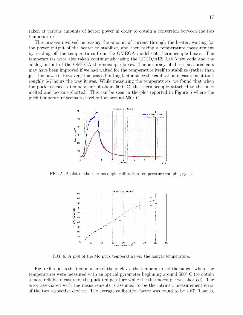
This process involved increasing the amount of current through the heater, waiting forthe power output of the heater to stabilize, and then taking a temperature measurementby reading off the temperatures from the OMEGA model 650 thermocouple boxes. Thetemperatures were also taken continuously using the LEED/AES Lab View code and theanalog output of the OMEGA thermocouple boxes. The accuracy of these measurementsmay have been improved if we had waited for the temperature itself to stabilize (rather thanjust the power). However, time was a limiting factor since the calibration measurement tookroughly 6-7 hours the way it was. While measuring the temperatures, we found that whenthe puck reached a temperature of about 500◦ C, the thermocouple attached to the puckmelted and became shorted. This can be seen in the plot reported in Figure 5 where thepuck temperature seems to level out at around 500◦ C.
FIG. 5. A plot of the thermocouple calibration temperature ramping cycle.
FIG. 6. A plot of the Mo puck temperature vs. the hanger temperature.
Figure 6 reports the temperature of the puck vs. the temperature of the hanger where thetemperatures were measured with an optical pyrometer beginning around 500◦ C (to obtaina more reliable measure of the puck temperature while the thermocouple was shorted). Theerror associated with the measurements is assumed to be the intrinsic measurement errorof the two respective devices. The average calibration factor was found to be 2.67. That is,
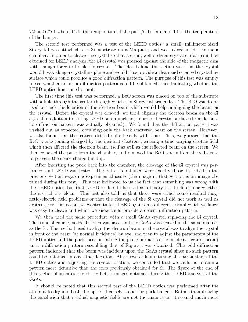
18
T2 ≈ 2.67T1 where T2 is the temperature of the puck/substrate and T1 is the temperatureof the hanger.
The second test performed was a test of the LEED optics: a small, millimeter sizedSi crystal was attached to a Si substrate on a Mo puck, and was placed inside the mainchamber. In order to cleave the crystal so that a clean, well-ordered crystal surface could beobtained for LEED analysis, the Si crystal was pressed against the side of the magnetic armwith enough force to break the crystal. The idea behind this action was that the crystalwould break along a crystalline plane and would thus provide a clean and oriented crystallinesurface which could produce a good diffraction pattern. The purpose of this test was simplyto see whether or not a diffraction pattern could be obtained, thus indicating whether theLEED optics functioned or not.
The first time this test was performed, a BeO screen was placed on top of the substratewith a hole through the center through which the Si crystal protruded. The BeO was to beused to track the location of the electron beam which would help in aligning the beam onthe crystal. Before the crystal was cleaved, we tried aligning the electron beam on the Sicrystal in addition to testing LEED on an unclean, unordered crystal surface (to make sureno diffraction pattern was actually obtained). We found that the diffraction pattern waswashed out as expected, obtaining only the back scattered beam on the screen. However,we also found that the pattern drifted quite heavily with time. Thus, we guessed that theBeO was becoming charged by the incident electrons, causing a time varying electric fieldwhich then affected the electron beam itself as well as the reflected beam on the screen. Wethen removed the puck from the chamber, and removed the BeO screen from the substrateto prevent the space charge buildup.
After inserting the puck back into the chamber, the cleavage of the Si crystal was per-formed and LEED was tested. The patterns obtained were exactly those described in theprevious section regarding experimental issues (the image in that section is an image ob-tained during this test). This test indicated to us the fact that something was wrong withthe LEED optics, but that LEED could still be used as a binary test to determine whetherthe crystal was clean. This test also told us that there were either some residual mag-netic/electric field problems or that the cleavage of the Si crystal did not work as well asdesired. For this reason, we wanted to test LEED again on a different crystal which we knewwas easy to cleave and which we knew could provide a decent diffraction pattern.
We then used the same procedure with a small GaAs crystal replacing the Si crystal.This time of course, no BeO screen was used and the GaAs was cleaved in the same manneras the Si. The method used to align the electron beam on the crystal was to align the crystalin front of the beam (at normal incidence) by eye, and then to adjust the parameters of theLEED optics and the puck location (along the plane normal to the incident electron beam)until a diffraction pattern resembling that of Figure 4 was obtained. This odd diffractionpattern indicated that the beam was incident upon the GaAs crystal since no such patterncould be obtained in any other location. After several hours tuning the parameters of theLEED optics and adjusting the crystal location, we concluded that we could not obtain apattern more definitive than the ones previously obtained for Si. The figure at the end ofthis section illustrates one of the better images obtained during the LEED analysis of theGaAs.
It should be noted that this second test of the LEED optics was performed after theattempt to degauss both the optics themselves and the puck hanger. Rather than drawingthe conclusion that residual magnetic fields are not the main issue, it seemed much more
19
likely in this case that the process of degaussing had no real effect on the fields produced bythe welding joints of the optics and the hanger itself. The best option is simply to replaceall of the 304 stainless steel in the hanger with 316 stainless steel. Good support for thisargument comes from the YAG screen test which indicates that the 304 stainless steel hangerpoles alter the direction of the beam.
The effect of an external magnetic field on the diffraction pattern was also tested usingthe GaAs crystal. This external field was provided by a 4 turn, 4.5 inch radius solenoidwhich created a field of strength 50-75 gauss at the center. The field was used as a trimmingfield to cancel out any residual fields in the vicinity of the electron beam. The solenoid wasplaced directly outside the section of the vacuum chamber containing the LEED optics. Itwas found that the effect of the trimming field on the diffraction pattern was only to movethe reflected beam (the brightest spot on the screen) in the vertical direction, regardless ofthe orientation of the solenoid. Thus, constructing Helmholtz coils to trim the field in thevicinity of the beam may slightly help the diffraction pattern, but it does not seem like itcould fix the biggest problem. The inefficacy of the trimming field may be due to the factthat the coils must reside outside the vacuum chamber. Additionally, it is difficult to orientthe coils in such a way that the electron beam resides in the homogeneous region of thesolenoid’s field due to the finite size of the coils and the various ports and valves around thechamber.
Finally, a test of the Ar ion gun and its ability to sputter a surface was performed. AGaAs wafer with a large oxidation layer was attached to a Mo puck (using indium solder)and placed inside the chamber. The puck was aligned by eye in front of the gun and, afterbackfilling the chamber to a pressure of 5e-05 Torr with Ar gas from a supply bottle, thefilament of the gun was degassed and prepped for use. The ion gun was then run with anemission current of 20 mA and a 2 kV filament voltage at normal incidence to the wafersurface. The focus of the beam was adjusted slightly from the factory setting so that thebeam appeared to come to a sharp point on the surface of the GaAs wafer. Figure 7illustrates the process of the Ar ion beam striking the GaAs surface.
The sputtering process would increase the vacuum level from 5e-05 Torr to about 3e-04Torr. When this occurred, the gun would be shut off, the chamber would be pumped downagain, and Ar gas would be let in to reestablish the required vacuum level. The total time theion gun was left to sputter was roughly 20 minutes. The location of the wafer with respectto the beam was then adjusted so that a second spot on the wafer was sputtered by thebeam at near-normal incidence. After sputtering this location for another 20 minutes, theion gun was shut off and the puck was removed from the chamber. Upon visual inspectionof the oxidized wafer, it was evident that the ion gun had essentially cleaned the spots whereit hit the oxidation layer. A picture of the wafer after removal from the chamber is givenin Figure 7. The orange part on the surface is the oxidation layer, and the blue in thecenter is where the ion gun broke through. This test successfully proved that the ion gunworked, that sputtering was a sufficient means of removing surface contaminants (or at leastoxidation layers), and that the gun was ready for use on the Mo substrates.
5. Mo Sample Preparation
The effect of the surface roughness of the Mo substrate on the various properties of thephotocathode (e.g. quantum efficiency) is something we would like to better understand.For this reason, we sought to prepare atomically flat Mo surfaces for the deposition of the
20
(a)LEED diffraction
pattern obtained
during the GaAs test.
(b)The Ar ion
sputtering process: the
ion beam is a faint
blue color.
(c)The oxidized GaAs
wafer used in the Ar
ion gun test.
FIG. 7. Pictures documenting the various tests of the new Mo sample preparation chamber.
multi-alkali photocathodes. In order to obtain an atomically flat substrate surface, severalsteps were taken: 99.9% pure Mo foil (∼1 mm thick) was first cut into disk shapes which fiton top of the Mo pucks. These disks had a roughness (in the form of grain-like scratches)which was quite noticeable, even to the naked eye. For this reason, heavy polishing of theMo disks was necessary. For this proof-of-principle experiment, two Mo substrates wereprepared via hand polishing: we began the process by using a 30 µm diamond suspensionrubbed into the disk using a clean cloth. A 15 µm fine sand paper was then used to reducethe roughness even further. This brought the disk to a near mirror polish, except for 4 or 5major scratches in the surface which could not be removed using this method.
In order to remove these deep scratches, a 400 grade sand paper was used: the sand paperwas wetted with water and then rubbed in a vertical motion, perpendicular to the grain ofthe scratches, into the disk. This was done continuously until the surface had a homogenousset of scratches in the direction of the motion of the sand paper (at this point, the majorscratches had disappeared). The sand paper was then rubbed in a direction perpendicularto this homogenous set of scratches. This procedure was then applied using 600 grade sandpaper. Next, a series of diamond suspension pastes were used to polish the disks along withcoconut-oil soap and isopropanol to wash the disks between polishes. Pastes of diamondparticle size 9 µm, 6 µm, 3 µm, 1 µm, 0.25 µm, and 0.1 µm were used in decreasing particlesize for this purpose.
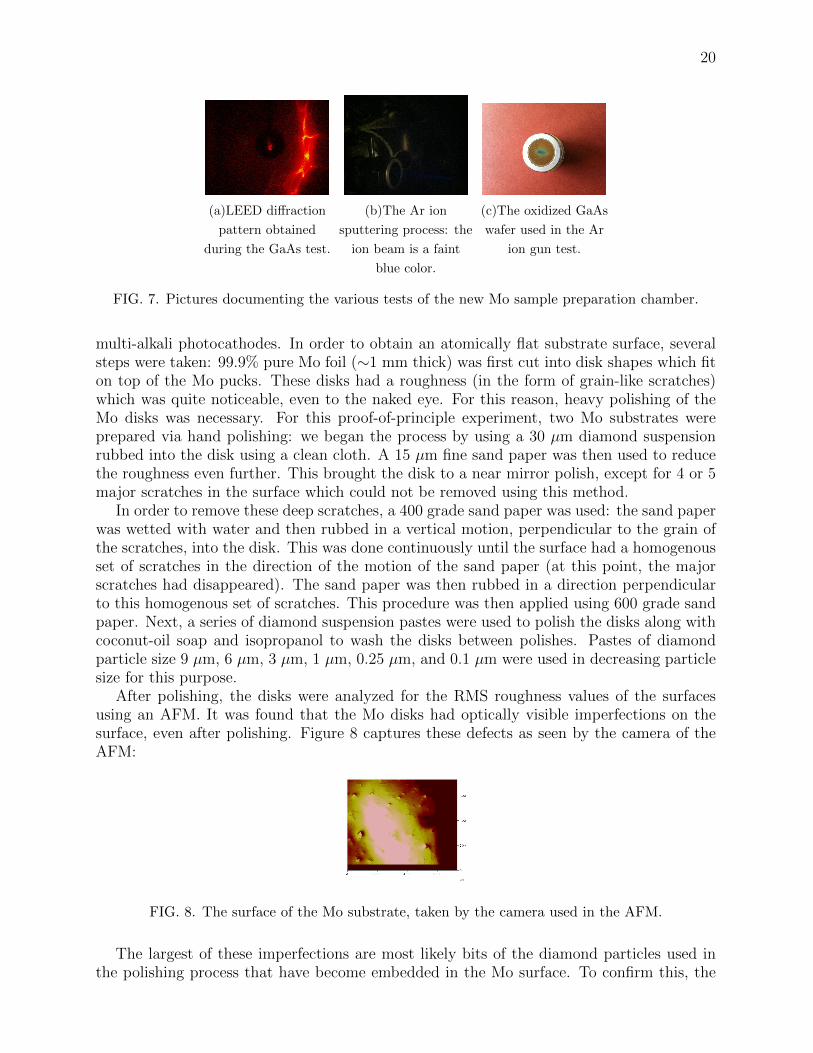
After polishing, the disks were analyzed for the RMS roughness values of the surfacesusing an AFM. It was found that the Mo disks had optically visible imperfections on thesurface, even after polishing. Figure 8 captures these defects as seen by the camera of theAFM:
FIG. 8. The surface of the Mo substrate, taken by the camera used in the AFM.
The largest of these imperfections are most likely bits of the diamond particles used inthe polishing process that have become embedded in the Mo surface. To confirm this, the

21
surface was analyzed using a scanning electron microscope (SEM) and energy dispersiveX-ray spectroscopy (EDX). The results of this analysis are presented in the Results andDiscussion section of this paper.
From the AFM scans of the two substrates, the surface appears to be relatively flat ona 1 micron scale. There are occasional imperfections (bumps) that tend to align in thesame direction, indicating that they are either a result of the polishing (from rubbing thesand paper and diamond suspensions in the same direction) or are characteristic of the Momaterial itself (like the grain of a piece of wood). On a 10 micron scale, the large cracks anddivots which are the large, optical imperfections come in to view. 3-D surface plots of boththe 10 micron and 1 micron scales for the two substrates, along with their associated RMSroughness values, are given in Figures 9 and 10.
(a)1 micron scale, RMS
roughness= 2.27nm
(b)1 micron scale, RMS
roughness= 2.64nm
(c)10 micron scale, RMS
roughness= 5.32nm
FIG. 9. Surface of hand polished Mo substrate (polished by Luca Cultrera)
(a)1 micron scale, RMS
roughness= 3.52nm
(b)10 micron scale, RMS
roughness= 18.95nm
FIG. 10. Surface of hand polished Mo substrate (polished by Matt Nichols)
The thermal annealing and sputtering process was used in an attempt to remove theselarge scale imperfections, and smooth out the surface. In the future, mechanical polishingwill be used for a more homogenous polish. It will also be worth testing electro polishingof the samples (in addition to mechanically polishing them) in order to improve the surfacequality.
After analyzing the samples with the AFM, the samples were separated according to theirroughness values: both samples underwent the sputtering/annealing process, but only onesubstrate (the flatter one) was used for the proof-of-principle experiment with the bi-alkaliphotocathode. The other substrate was analyzed with the AFM again after the sputter-ing/annealing process to determine the process’ effect on the surface. The substrate usedfor the photocathode deposition underwent a 3-stage sputtering/annealing process: the de-tails of this process are described in the Experimental Setup portion of this report. This wasthe first test of the sputtering/annealing process on an actual Mo substrate, and everythingworked correctly except for one detail which is worth noting: during the first annealing cycleof the 3-stage process, a small droplet of indium formed near the edge of the tantalum cap

22
which holds the substrate in place on the puck. A picture of this droplet and the annealingprocess is given in Figure 11.
This droplet consists of the indium solder used to glue the substrate to the face of thepuck. In this particular instance, apparently too much solder was used, and it pooled downnear the bottom of the substrate. This droplet was large enough to prevent the puck,once the photocathode was deposited, from being placed inside the ERL DC electron gun.However, once the photocathode was deposited on the substrate surface, it was still possibleto accurately measure the spectral response of the photocathode and determine the effectof the substrate on these measurements: the Results and Discussion section details theseresults. A description of the deposition process is also given in the Results and Discussionsection of this report.
FIG. 11. The annealing of the Mo substrate and the melted indium droplet.
The second Mo substrate (the slightly rougher one) underwent a 2-stage sputter-ing/annealing process. While preparing the puck and substrate for this process, a lesseramount of indium solder was used in order to prevent the pooling of the solder at the bottomof the substrate. This was done in case the success of the sputtering/annealing process onthis substrate warranted its future use as a bi-alkali photocathode test substrate. As itturned out however, it was found that even with the use of less solder, a droplet still formed.This occurred when the puck temperature exceeded 850◦ C. After the sputtering/annealingprocess, the disk was analyzed with the SEM/EDX, and was then brought back to the AFMto determine if the annealing had sufficiently smoothed out the surface (e.g. removed thelarge scale defects). The results of this test are given in the Results and Discussion sectionof this report.
C. Results and Discussion
1. SEM and EDX Analysis of Polished Mo Substrate
After completing the 2 stage sputtering/annealing process for the rougher substrate, thedisk was taken to the SEM/EDX to analyze the surface for its constituents: we wantedto know whether the large scale lumps we had seen on the surface with the AFM wereactually bits of Mo, or whether they were bits of diamond that had lodged themselves intothe Mo surface during the polishing process. Figures 12 and 13 show SEM micrographs andEDX spectra of two of the particles we found on the Mo surface. The EDX spectra revealthat both particles have a major carbon peak. This indicates to us that some of the large

23
imperfections are in fact bits of diamond that have stuck to the surface. This may warrantthe use of electrochemical polishing of the surface in future endeavors to avoid this problem.
Figure 14 reveals lots of large scale holes and pits that do not appear to be made ofdiamond. These pits act as an indication that the annealing may not have been as successfulas we had hoped: the pits are on the order of several microns in diameter, which means thesurface is still fairly rough. This may simply mean however that the annealing processes usedfor this particular puck did not reach high enough temperatures or that these temperatureswere not maintained for a long enough time. To analyze these structures even further, thesubstrate was taken to the AFM for analysis.
(a)SEM image of
1st particle
(∼1000µm wide)
(b)EDX scan of first particle indicates presence of
carbon
FIG. 12. Foreign particle on the polished and annealed Mo surface
(a)SEM image of
2nd particle
(∼1000-2000µm
wide)
(b)EDX scan of second particle indicates again
the presence of carbon
FIG. 13. Another foreign particle on the polished and annealed Mo surface
2. AFM Analysis of Annealed Mo Substrate
Initially viewing the prepared Mo surface from the AFM camera’s view point (withoutactually performing a scan) revealed large scale bumps similar to those on the surface beforethe sputtering/annealing process. This again indicates that either the annealing processdoes not help to make the surface smoother, or that the specific procedure was not con-ducted thoroughly enough. 10 micron and 50 micron scale maps of the Mo surface afterthe sputtering/annealing process are given in Figure 15 along with their associated RMSroughness values. The 10 micron scale maps do not reveal anything new since the RMS

24
(a)SEM image
indicating
irregularities
(b)Closer SEM image
emphasizing the
surface defects
FIG. 14. SEM micrographs of the polished and annealed Mo surface which indicate large scale
irregularities
roughness values are still on the order of a few nanometers, and in general the roughness ofa surface changes significantly from location to location (especially on a 10 micron scale).
The 50 micron scale however reveals some of the pits that had been seen on the SEMscan: these pits are around 5-10 microns in diameter. One of the deepest pits reaches about30 microns in depth. This means that there is still some significant roughness to the surfacethat could be eliminated. This may of course be due to the fact that this surface was notpolished as thoroughly as the first substrate, but given the fact that a significant amount ofeffort went in to polishing even this surface, a mechanical or electro polishing option seemsalmost necessary. This is especially true if the Mo turns out to be a successful pursuit (interms of improving the QE of the photocathodes) in which case dozens of substrates will beneeded.
(a)10 micron scale, RMS
roughness= 7.43nm
(b)10 micron scale, RMS
roughness= 7.46nm
(c)50 micron scale, RMS
roughness= 4.05µm
FIG. 15. Surface of Mo substrate (polished by Luca Cultrera) after a 2-stage sputtering and
annealing process
3. Spectral Response of CsK2Sb Photocathode Grown on Mo (100) Substrate
Once the bi-alkali photocathode had been deposited on the flatter of the two Mo sub-strates, a spectral response measurement was taken in order to determine whether or notthe Mo substrate had any beneficial effects. The spectral response was measured usinga monochromator: light of varying wavelengths was shown on the photocathode, and theQE was measured at each value of the wavelength. The plot of the spectral response ofthis cathode is given in Figure 16 and is graphed along with the spectral responses of the

25
CsK2Sb photocathode grown on the Si (100) substrate and the Cs3Sb photocathode. Fromthe data obtained, it is evident that for wavelengths less than about 600 nm, the CsK2Sbcathode grown on the Mo substrate has a significantly higher QE than that grown on the Sisubstrate. In fact, at 520 nm (green), it appears that the Mo substrate cathode has a QEthat is approximately a factor of 2 higher than the Si substrate cathode. This is exactly thefactor of two we were looking for from this project.
The success of this experiment does not, however, necessarily indicate the ability of the Mosubstrate to improve the QE of the CsK2Sb photocathode. In fact, the significant contrastin QE between the two cathodes may be due to several other factors. First and foremost,it is possible that the original cathode was not grown properly: it may be that the cathodewe thought was made of CsK2Sb might actually have a different stoichiometry. Secondly,the deposition process used to form the Mo substrate photocathode differed slightly fromthat of the Si substrate cathode. The difference between the two formation processes was inthe temperature used to make the deposition. For the Mo substrate cathode, the followingrecipe was used: Sb was evaporated on the surface until a 15 nm layer had been formed. Thisoccurred while the substrate cooled from 180◦C to 140◦C. Then, K was evaporated onto theSb layer, while the temperature cooled from 130◦C to 100◦C, until the photocurrent emittedby the cathode hit a peak value. Finally, Cs was added while the substrate cooled from100◦C to 80◦C until another photocurrent peak was obtained . The process used for the Sisubstrate cathode was very similar except that it began at about 160◦C rather than 180◦C.
The fact remains however that a significantly higher QE was obtained for this cathodein the portion of the spectrum that is most significant to the purposes of the ERL injector.While the other two possibilities may have played a role in the difference between the QE’sof the two cathodes, the Mo substrate may also have made a significant contribution. Thus,a more detailed investigation into the use of Mo substrates on CsK2Sb photocathodes, thatgoes beyond the scope and time of this project, must be conducted.
FIG. 16. Spectral response of CsK2Sb and Cs3Sb photocathodes on different substrates.
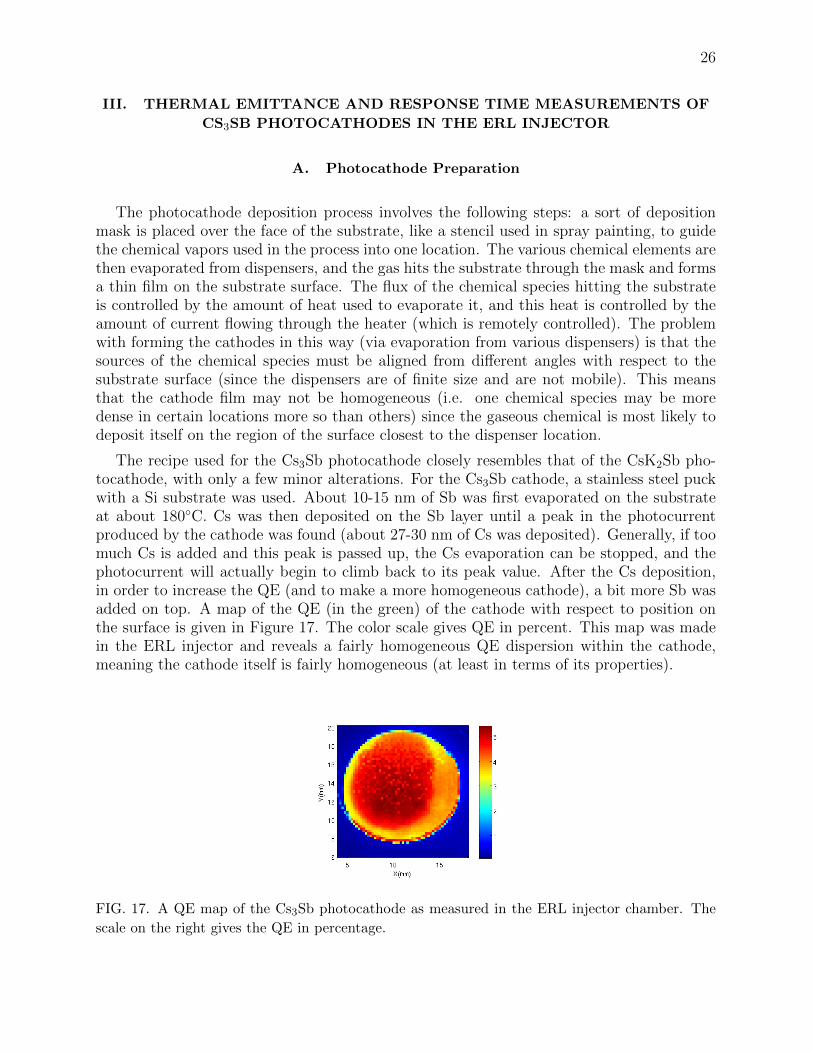
26
III. THERMAL EMITTANCE AND RESPONSE TIME MEASUREMENTS OF
CS3SB PHOTOCATHODES IN THE ERL INJECTOR
A. Photocathode Preparation
The photocathode deposition process involves the following steps: a sort of depositionmask is placed over the face of the substrate, like a stencil used in spray painting, to guidethe chemical vapors used in the process into one location. The various chemical elements arethen evaporated from dispensers, and the gas hits the substrate through the mask and formsa thin film on the substrate surface. The flux of the chemical species hitting the substrateis controlled by the amount of heat used to evaporate it, and this heat is controlled by theamount of current flowing through the heater (which is remotely controlled). The problemwith forming the cathodes in this way (via evaporation from various dispensers) is that thesources of the chemical species must be aligned from different angles with respect to thesubstrate surface (since the dispensers are of finite size and are not mobile). This meansthat the cathode film may not be homogeneous (i.e. one chemical species may be moredense in certain locations more so than others) since the gaseous chemical is most likely todeposit itself on the region of the surface closest to the dispenser location.
The recipe used for the Cs3Sb photocathode closely resembles that of the CsK2Sb pho-tocathode, with only a few minor alterations. For the Cs3Sb cathode, a stainless steel puckwith a Si substrate was used. About 10-15 nm of Sb was first evaporated on the substrateat about 180◦C. Cs was then deposited on the Sb layer until a peak in the photocurrentproduced by the cathode was found (about 27-30 nm of Cs was deposited). Generally, if toomuch Cs is added and this peak is passed up, the Cs evaporation can be stopped, and thephotocurrent will actually begin to climb back to its peak value. After the Cs deposition,in order to increase the QE (and to make a more homogeneous cathode), a bit more Sb wasadded on top. A map of the QE (in the green) of the cathode with respect to position onthe surface is given in Figure 17. The color scale gives QE in percent. This map was madein the ERL injector and reveals a fairly homogeneous QE dispersion within the cathode,meaning the cathode itself is fairly homogeneous (at least in terms of its properties).
FIG. 17. A QE map of the Cs3Sb photocathode as measured in the ERL injector chamber. The
scale on the right gives the QE in percentage.
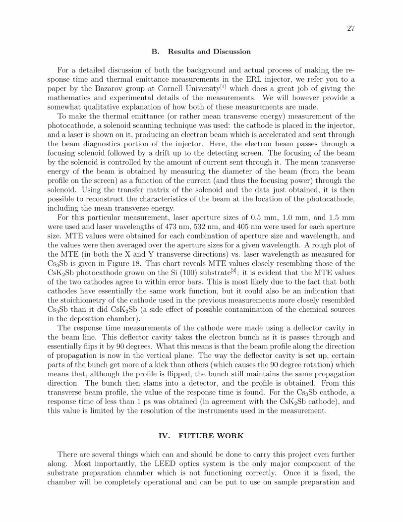
27
B. Results and Discussion
For a detailed discussion of both the background and actual process of making the re-sponse time and thermal emittance measurements in the ERL injector, we refer you to apaper by the Bazarov group at Cornell University[1] which does a great job of giving themathematics and experimental details of the measurements. We will however provide asomewhat qualitative explanation of how both of these measurements are made.
To make the thermal emittance (or rather mean transverse energy) measurement of thephotocathode, a solenoid scanning technique was used: the cathode is placed in the injector,and a laser is shown on it, producing an electron beam which is accelerated and sent throughthe beam diagnostics portion of the injector. Here, the electron beam passes through afocusing solenoid followed by a drift up to the detecting screen. The focusing of the beamby the solenoid is controlled by the amount of current sent through it. The mean transverseenergy of the beam is obtained by measuring the diameter of the beam (from the beamprofile on the screen) as a function of the current (and thus the focusing power) through thesolenoid. Using the transfer matrix of the solenoid and the data just obtained, it is thenpossible to reconstruct the characteristics of the beam at the location of the photocathode,including the mean transverse energy.
For this particular measurement, laser aperture sizes of 0.5 mm, 1.0 mm, and 1.5 mmwere used and laser wavelengths of 473 nm, 532 nm, and 405 nm were used for each aperturesize. MTE values were obtained for each combination of aperture size and wavelength, andthe values were then averaged over the aperture sizes for a given wavelength. A rough plot ofthe MTE (in both the X and Y transverse directions) vs. laser wavelength as measured forCs3Sb is given in Figure 18. This chart reveals MTE values closely resembling those of theCsK2Sb photocathode grown on the Si (100) substrate[3]: it is evident that the MTE valuesof the two cathodes agree to within error bars. This is most likely due to the fact that bothcathodes have essentially the same work function, but it could also be an indication thatthe stoichiometry of the cathode used in the previous measurements more closely resembledCs3Sb than it did CsK2Sb (a side effect of possible contamination of the chemical sourcesin the deposition chamber).
The response time measurements of the cathode were made using a deflector cavity inthe beam line. This deflector cavity takes the electron bunch as it is passes through andessentially flips it by 90 degrees. What this means is that the beam profile along the directionof propagation is now in the vertical plane. The way the deflector cavity is set up, certainparts of the bunch get more of a kick than others (which causes the 90 degree rotation) whichmeans that, although the profile is flipped, the bunch still maintains the same propagationdirection. The bunch then slams into a detector, and the profile is obtained. From thistransverse beam profile, the value of the response time is found. For the Cs3Sb cathode, aresponse time of less than 1 ps was obtained (in agreement with the CsK2Sb cathode), andthis value is limited by the resolution of the instruments used in the measurement.
IV. FUTURE WORK
There are several things which can and should be done to carry this project even furtheralong. Most importantly, the LEED optics system is the only major component of thesubstrate preparation chamber which is not functioning correctly. Once it is fixed, thechamber will be completely operational and can be put to use on sample preparation and
28
FIG. 18. A graph of the X and Y mean transverse energy values of the Cs3Sb photocathode vs.
incident laser wavelength.
surface diagnostics. Therefore, one of the first things that can be done is to bring the LEEDsystem to an operational state. This will involve replacing the 304 stainless steel in thehanger assembly with 316 stainless steel in order to reduce the magnetic field produced bythe hanger poles surrounding the puck. It is possible that the heater, which is essentially justa big resistor, is producing a magnetic field which magnetizes the hanger poles. The polescould then retain this magnetization and distort the LEED electron beam. 316 stainlesssteel is less magnetic, so this problem will be avoided by changing the metal of the assembly.Additionally, it should be checked as to whether or not the insulators within the LEEDoptics grids are building up electric charge and distorting the beam. Trimming magneticfields may also be added using Helmholtz coils to negate any residual fields in the vicinityof the optics.
A second thing that should be done is to test the newly deposited CsK2Sb photocathodein the ERL injector to obtain both a QE map of the cathode and to test its thermal emittanceand response time. If this is not possible due to the droplet of indium solder on the surface,another photocathode should be grown using a similar process and should have these valuesmeasured. However, in order to conduct this last step, the problem with the indium soldermelting during annealing must be solved. It was eventually found that increasing the heatercurrent beyond 12 A will cause the solder to melt and pool at the bottom. Two solutionsto this problem which will still allow for heating up to extreme temperatures are the use ofa tantalum cap alone (no solder whatsoever) to hold the substrate on and the use of a Mopuck which has a flat top which would be polished (and thus a separate substrate attachedto the puck would not be needed).
A final thing that should be done to see this project all the way through would be toinvestigate further the effect of the Mo substrates on the CsK2Sb photocathode’s photoemis-sive properties. Although the QE does seem to have improved with respect to the cathodegrown on the Si substrate, this does not mean the Mo substrate had anything to do with it.In the next steps, more Mo substrates should be prepared and tested with the photocath-ode. These substrates should be prepared even more rigorously than the ones made for thisproject’s purpose. This may involve even more time spent hand polishing the samples, more
29
time annealing and sputtering, and higher temperatures used during the annealing process.Additionally, this may involve the use of mechanical and electropolishing of the Mo samplesto test their particular effects on the surface roughness. As a control, a second Si substratephotocathode should be grown to test whether the lower QE was simply a fluke or whetherit was actually a real characteristic property of the cathode.
V. CONCLUSIONS
Preparing the Mo substrates using hand polishing, Ar ion sputtering, and thermal anneal-ing for the deposition of a bi-alkali antimonide photocathode seemed to have a positive effecton that cathode’s QE (increased by a factor of 2). It is not known however if this preparationprocess truly benefitted the cathode or even if the substrate itself helped increase the QE.The hand polishing was able to bring the substrate to a mirror polish, and was able to bringthe surface to nm flatness in most locations, with large scale (5-10 micron) bumps/pits inseveral locations. Some of the irregularities on the Mo surface after the preparation were infact due to the diamond particles used during the polishing process. For the measurementsof the Cs3Sb photocathode thermal emittance and response time, it was found that both themean transverse energy and the response time were within error bars of the CsK2Sb photo-cathode grown on the Si substrate which was measured earlier. This may be an indicationthat the stoichiometry of the CsK2Sb photocathode used in previous measurements is notquite that of CsK2Sb (it may in fact have been something resembling that of CS3Sb). Thiscould explain the difference between the Mo substrate cathode’s QE and the Si substratecathode’s QE (if the Mo substrate cathode had a more accurate stoichiometry).
VI. ACKNOWLEDGEMENTS
I would like to thank Luca Cultrera for being such a knowledgeable and helpful advisoron this project. I would also like to thank Ivan Bazarov for providing intellectual insightand guidance. Joe Conway, Toby Moore, Richard Merluzzi, John Dobbins, Karl Smolenski,Siddharth Karkare, and Adam Bartnik also made countless significant contributions whichhelped get this project up and running. This work was supported by NSF PHY 0849885,NSF DMR-0807731, and DOE DE-SC0003965.
[1] I. Bazarov, B.M. Dunham, Y. Li, X. Liu, D.G. Ouzounov, C.K. Sinclair, F. Hannon, and T.
Miyajima., J. Appl. Phys.., 103, 054901 (2008).
[2] L. Cultrera., Proceedings of 2011 Partical Accelerator Conference, New York, NY, THOCN1,
2011.
[3] I. Bazarov, L. Cultrera, A. Bartnik, B. Dunham, S. Karkare, Y. Li, X. Liu, J. Maxson, and W.
Roussel., Appl. Phys. Lett. 98, 224101 (2011).


![Schottky Barrier Heights Extraction of an Atomically Flat Ni ...Schottky-Barrier MOSFET Technology”, IEEE Transactions on Electron Devices, 53, p.1048-p.1058 (2006) [1.4] W. Mizubayashi,](https://img.pdfslide.us/doc/110x75/60e94ab2f3e0e511165d0cec/schottky-barrier-heights-extraction-of-an-atomically-flat-ni-schottky-barrier.jpg)