Embed Size (px)
Citation preview

This content has been downloaded from IOPscience. Please scroll down to see the full text.
Download details:
IP Address: 147.46.122.160
This content was downloaded on 01/12/2013 at 23:59
Please note that terms and conditions apply.
Preparation via an electrochemical method of graphene films coated on both sides with NiO
nanoparticles for use as high-performance lithium ion anodes
View the table of contents for this issue, or go to the journal homepage for more
2013 Nanotechnology 24 475402
(http://iopscience.iop.org/0957-4484/24/47/475402)
Home Search Collections Journals About Contact us My IOPscience

IOP PUBLISHING NANOTECHNOLOGY
Nanotechnology 24 (2013) 475402 (8pp) doi:10.1088/0957-4484/24/47/475402
Preparation via an electrochemicalmethod of graphene films coated on bothsides with NiO nanoparticles for use ashigh-performance lithium ion anodes
Gil-Pyo Kim, Inho Nam, Soomin Park, Junsu Park and Jongheop Yi
World Class University Program of Chemical Convergence for Energy and Environment, School ofChemical and Biological Engineering, College of Engineering, Seoul National University, Shillim-dong,Kwanak-gu, Seoul 151-742, Korea
E-mail: [email protected]
Received 1 September 2013, in final form 4 October 2013Published 5 November 2013Online at stacks.iop.org/Nano/24/475402
AbstractWe report on a simple strategy for the direct synthesis of a thin film comprising interconnected NiOnanoparticles deposited on both sides of a graphene sheet via cathodic deposition. For theco-electrodeposition, graphene oxide (GO) is treated with water-soluble cationic poly(ethyleneimine)(PEI) which acts as a stabilizer and trapping agent to form complexes of GO and Ni2+. The positivelycharged complexes migrate toward the stainless steel substrate, resulting in the electrochemicaldeposition of PEI-modified GO/Ni(OH)2 at the electrode surface under an applied electric field. Theas-synthesized film is then converted to graphene/NiO after annealing at 350 ◦C. The interconnected NiOnanoparticles are uniformly deposited on both sides of the graphene surface, as evidenced by fieldemission scanning electron microscopy, transmission electron microscopy and energy dispersivespectrometry. This graphene/NiO structure shows enhanced electrochemical performance with a largereversible capacity, good cyclic performance and improved electronic conductivity as an anode materialfor lithium ion batteries. A reversible capacity is retained above 586 mA h g−1 after 50 cycles. Thefindings reported herein suggest that this strategy can be effectively used to overcome a bottleneckproblem associated with the electrochemical production of graphene/metal oxide films for lithium ionbattery anodes.
(Some figures may appear in colour only in the online journal)
1. Introduction
Due to its superior electronic conductivity, structuralflexibility and chemical stability, graphene, a new type oftwo-dimensional carbon material, represents an advancedmaterial that promises to find use in lithium ion batteries(LIBs) [1–3]. However, the irreversible aggregation andrestacking of graphene sheets, which lead to changes in itsintrinsic chemical and physical properties during the reductionprocess, are problems that limit its practical applications[4, 5]. To circumvent this, graphene-based compositematerials, including transition metal oxides such as SnO2 [3],
Co3O4 [6], NiO [7] and Fe2O3 [8] have been exploitedfor use as anode materials for LIBs. The incorporationof metal oxides into graphene layers could reduce thedegree of stacking of graphene sheets as well as generateelectron-conducting and ion-transporting pathways [9–11].In addition, the excellent flexibility of graphene canefficiently buffer the volume expansion associated withthe Li charge/discharge process [9–11]. Graphene/metaloxide composites are typically prepared by the thermal orchemical reduction of graphene oxide (GO) and metallicprecursors [6–8]. However, the above-mentioned methodsobviously involve highly toxic chemicals or high temperatures
10957-4484/13/475402+08$33.00 c© 2013 IOP Publishing Ltd Printed in the UK & the USA

Nanotechnology 24 (2013) 475402 G-P Kim et al
and, moreover, multiple steps are required. Consequently, amore efficient process that includes a shorter processing timeand a simplified setup for production is needed.
Electrodeposition is an effective technique that is used forthe synthesis of metal oxide thin films, in which the thickness,density and morphology can be easily controlled by adjustingthe applied current, bath chemistry and temperature [12–14].Such an electrochemical method has recently been usedfor the synthesis of graphene and graphene-based metaloxide films, and has been found to be a simple andeasily used tool [15–21]. However, most of the currentlyproposed methods typically involve two steps. A GO textileelectrode is first prepared by a coating process such asdip-coating, drop-casting or spray-coating. This is followedby an electrochemical synthesis with a metallic precursor thatis achieved by simply dipping the graphene textile electrodeinto a precursor solution and subsequently performingelectrodeposition. As a result, metal oxide nanoparticlesare mostly located on the surface of the graphene textileelectrode, resulting in an increase in the degree of stackingof graphene sheets [15–19]. More importantly, in the caseof the co-electrodeposition of graphene/metal composite, itis necessary to use negatively charged metallic precursors[20, 21]. The cationic metallic precursors could presumablyact as cross-linkers due to their tendency to bind readily to theoxygen functional groups of GO, leading to the precipitationand agglomeration of GO in the solution [20, 22]. To addresssuch critical problems, our previous work demonstrated thatthe modification of GO by treatment with poly(ethyleneimine)(PEI) is a reliable method for coexisting and chelating withpositively charged metallic precursors, and also makes itpossible to simultaneously synthesize graphene/metal oxidethin films [23].
Graphene/NiO is one of the promising anode materialsfor use in LIBs due to its extra high capacity compared topristine graphene and NiO electrodes [7, 24, 25]. However,like other conversion-based anode materials, its practicalapplication to LIBs is greatly restrained by detrimentaleffects related to its structural and electrochemical propertiesupon cycling because of the non-intimate contact betweengraphene layers and NiO nanoparticles, which would lead toa loss of electrical contact and subsequent capacity fading.In addition, the process of fabricating electrodes continuesto be both time-consuming and labor-intensive. Herein,we report on attempts to expand our previously reportedco-electrodeposition methodology by using PEI-modifiedGO (PEI-GO). The developed method is very simplecompared with previously reported methods for the synthesisof NiO/graphene films. Due to the ease of formationof PEI/Ni2+ complexes with a high stability [26], thecomplexation of PEI-GO and Ni2+ ions would effectivelypermit migration to the substrate, which could subsequentlypermit the interconnected NiO nanoparticles to coat bothsides of the graphene surface during the electrodepositionprocedure. The as-synthesized material efficiently utilizes thecombined merits of NiO and graphene, resulting in a productwith superior performance with a large reversible capacity,excellent cycling stability and enhanced conductivity.
2. Experimental details
2.1. Preparation of PEI-GO
The GO was initially synthesized by the chemical exfoliationof commercially available graphite powder by a previouslyreported method [27]. First, a 0.3 g sample of GO wasdispersed in 200 ml of de-ionized (DI) water by sonication for1 h, and then transferred to a three-necked round-bottomedflask. A 0.1 g sample of PEI was added to the abovesolution and the resulting suspension was stirred at 60 ◦Cfor 12 h to ensure complete reaction. After cooling toroom temperature, the obtained dispersion was isolated bycentrifugation (15 000 rpm for 30 min) and the solid materialwashed with DI water three times to remove excess PEI.
2.2. Electrodeposition of graphene/NiO thin film
The electrodeposition was performed at room temperatureusing the WPG100 electrochemical workstation (WonAtech)with a three-electrode system. A clean piece of stainless steelfoil (SS) was used as the working electrode. A Pt plate andAg/AgCl were used as the counter electrode and referenceelectrode, respectively. The PEI-GO was redispersed in DIwater and 0.05 M of Ni(NO3)2 and 0.075 M of NaNO3were added to the solution. The co-electrodeposition wasperformed potentiostatically at −1.0 V (versus Ag/AgCl) for300 s. The resulting films were then rinsed with DI water toeliminate residual solvent, and then dried at room temperaturefor 6 h. Finally, the samples were annealed at 350 ◦C for 2 hunder a nitrogen atmosphere. For the sake of comparison, wesynthesized a pure NiO film by the same procedure withoutPEI-GO for 300 s.
2.3. Material characterization
The graphene/NiO films were characterized by a scanningelectron microscope (SEM; Carl Zeiss., SUPRA 55VP),transmission electron microscope (TEM; JEOL, JEM-2100),energy dispersive spectrometer (EDS; Bruker, Xflash5030detector), zeta-potential analyzer (Otsuka, ELS-Z), x-ray photoelectron spectroscope (XPS; Thermo, K-Alpha),thermogravimetric analyzer (TGA; Perkin Elmer, TG/DTA6300) and x-ray diffractometer (XRD; Rigaku, D/max-2200).Electrochemical characterization was performed on a batterytester (WonA tech, WBCS3000) and an electrochemicalworkstation (WonA tech, ZIVE SP2) using a conventionalcoin cell (CR2032) assembled in an argon-filled glove box.A lithium foil and microporous polypropylene were used asthe negative electrode and separator, respectively. A 1 Msolution of LiPF6 in a mixture of ethyl carbonate and diethylcarbonate (1:1 vol. ratio) was used as the electrolyte. Theelectrode capacity was measured by the galvanostatic chargeand discharge method with a constant current density of359 mA g−1 (0.5 C) in the voltage range of 0.01–3.0 V. Thefrequency of electrochemical impedance spectroscopy (EIS)ranged from 0.01 Hz to 200 kHz at the open circuit potential.
2

Nanotechnology 24 (2013) 475402 G-P Kim et al
3. Results and discussion
Scheme 1 illustrates the synthetic procedure used to preparea PEI-GO/Ni(OH)2 film by co-electrodeposition. Typically,individual GO sheets can be easily crosslinked in the presenceof cationic metal precursors such as Ni2+ and Co2+, leadingto agglomeration and precipitation of the GO [20, 22]. In orderto address this problem, the GO is chemically modified inthe presence of PEI as a stabilizer. Because the water-solublePEI is covalently linked to the GO sheet by the formation ofamide bonds, it can be immobilized on the surface of the GO,resulting in well dispersed positively charged (∼48.3 mV)GO-based materials. In addition, molecules of PEI containingamino and imino groups enabled stable chelates to be formedwith transition metal ions [23, 28]. Consequently, PEI-GOcould not only coexist with cationic metallic precursors butcould also play a key role in sequential complexation betweenGO and Ni2+. When the PEI-GOs/Ni2+ complex arrives atthe SS substrate, electrochemical reduction of the GO canoccur under cathodic conditions, which allows electrons to beconducted to the outer layer of the graphene sheet [17–20].As a result, the nickel ions chelated at the surface of PEI-GOare easily converted into Ni(OH)2 on the surface of the GO assuggested by the following reaction [28, 29]:
NO−3 + H2O+ 2e− → NO−2 + 2OH− (1)
Ni2+ + 2OH− → Ni(OH)2. (2)
The hydroxide ion (OH−) is produced by the reduction ofNO−3 under cathodic conditions. The generation of OH−
close to the cathode increases the local pH, resulting inthe precipitation of Ni(OH)2. The Ni(OH)2 continues todeposit through the transport of freely moving Ni2+ ionsin the solution. Afterwards, the PEI-GO/Ni(OH)2 film issubsequently converted into graphene/NiO by calcination at350 ◦C under a nitrogen atmosphere. Thus, the synthesis ofgraphene/NiO can be achieved by co-electrodeposition.
The morphology of the as-synthesized films was studiedby TEM as shown in figure 1. Figures 1(a) and (b)show the as-prepared PEI-GO/Ni(OH)2 thin film beforethe heat treatment, from which it can be clearly seen thatthe Ni(OH)2 films are directly deposited on the thin GOlayer. After annealing at 350 ◦C for 2 h, the interconnectedNiO nanoparticles are uniformly coated on graphene sheets(figures 1(c) and (d)). The existence of GO and graphenecan be determined by the graphene structure with thin layersobserved on the edge of the samples (arrow area in figures 1(b)and (d)).
The SEM images of electrodeposited thin films beforeand after the heat treatment are shown in figure 2.The electrodeposited Ni(OH)2 film without GO has ahomogeneous dense structure which is comprised of largegrains representing aggregates of small nanoscale-sizedparticles (figures 2(a) and (b)). In the case of thePEI-GO/Ni(OH)2, the as-prepared thin film appear to bewell deposited on the substrate surface, resulting in auniform coating of a loosely packed Ni(OH)2 nanoparticlenetwork on the GO (figure 2(c)). The formation of a
Scheme 1. Schematic representation of the fabrication process usedfor preparing PEI-GO/Ni(OH)2 films by co-electrodeposition.
hierarchical morphology of Ni(OH)2 nanoparticles is clearlyobserved. Figure 2(d), which shows the graphene/NiO filmafter calcination, confirms that the interconnected NiOnanoparticles are strongly anchored to the graphene sheets.Due to high-density deposition of NiO, the graphene isnot seen directly in the images. The above results stronglyindicate that the PEI treatment plays a significant rolein the co-electrodeposition process when cationic metallicprecursors are used. In addition, the NiO nanoparticle coatinglayer acts as spacers on both sides of graphene surface,effectively preventing the aggregation and restacking ofgraphene sheets upon cycling. Consequently, this favorablestructure could permit a large electrode/electrolyte contactarea to be maintained.
To further confirm the distribution of graphenenanosheets, EDS mapping was employed (figure 3). TheSEM image in figure 3(a) indicates that a thin layer ofgraphene/NiO is homogeneously deposited on the substrate.The corresponding elemental mapping of Ni (figure 3(b)) andcarbon (figure 3(c)) shows that both the nickel oxide andgraphene are distributed uniformly on the electrode surface.From the above result, a highly uniform graphene/NiO thinfilm is successfully synthesized by co-electrodeposition. Inaddition, it can be concluded that the PEI-GO/Ni2+ complexwould efficiently migrate to the SS substrate under the appliedelectric field. Moreover, well-distributed graphene sheetswould play an important role as a conductive network withinthe deposited layers, leading to enhanced electrochemicalperformance.
The as-deposited films (after drying at room temperature)were confirmed to be amorphous (data not shown). Figure 4displays XRD diffraction patterns for the electrodepositedNiO and graphene/NiO thin films on a stainless steel substrateafter calcination at 350 ◦C under a nitrogen atmosphere.For both films, the main diffraction lines at 37.2, 43.3 and62.8◦ correspond to the (111), (200) and (220) crystalline
3

Nanotechnology 24 (2013) 475402 G-P Kim et al
Figure 1. TEM images of electrodeposited thin films: (a) and (b) PEI-GO/Ni(OH)2, (c) and (d) graphene/NiO.
Figure 2. SEM images of electrodeposited thin films: (a) and (b) Ni(OH)2, (c) PEI-GO/ Ni(OH)2, (d) graphene/NiO.
phases of cubic NiO (JCPDS 47-1049), respectively [30].This result clearly indicates that the deposited Ni(OH)2 isconverted into nickel oxide as the result of the heat treatment.
For the graphene/NiO thin film, the diffraction peak ofgraphene was not observed because a relatively small amountof graphene component compared with that of NiO could be
4

Nanotechnology 24 (2013) 475402 G-P Kim et al
Figure 3. EDS atomic analysis results of graphene/NiO film:(a) SEM image of thin film, (b) nickel, and (c) carbon.
electrodeposited. The existence of graphene was confirmedby EDS (see figure 3(c)). Furthermore, the graphene contentwas determined to be approximately 12.7 wt%, from TGAmeasurement (data not shown).
XPS spectra of co-electrodeposited graphene/NiO filmsbefore and after calcination are shown in figure 5. Asshown in figure 5(a), the appearance of a N 1s peakbefore the heat treatment clearly indicates that the PEIchains were absorbed onto the GO. In addition, the N1s spectrum of electrodeposited PEI-GO/Ni(OH)2 beforecalcination shows pronounced peaks at 400.6 and 399.4 eV,corresponding to –NH2 and –NH–C=O functionalities,respectively (figure 5(b)) [28, 31]. Because the PEI chainscontain large numbers of –NH2 groups, it is reasonable toassume that the PEI would be grafted onto the surface ofthe GO by the formation of amide bonds. Furthermore, theXPS spectrum of a co-electrodeposited film after calcinationconfirms that the PEI chains are completely eliminated fromthe resulting graphene/NiO film (figures 5(a) and (b)) [23].
Figure 4. XRD spectra of NiO and graphene/NiO thin films aftercalcination at 350 ◦C.
Figure 5. XPS spectra of graphene/NiO thin films before and aftercalcination. (a) Wide scan survey spectra and (b) XPS N 1sspectrum of as-synthesized films.
The electrochemical performances of the electrode-posited pure NiO and graphene/NiO thin films were evaluatedusing a standard coin cell. Figures 6(a) and (b) show theinitial two charge–discharge curves for the pure NiO andgraphene/NiO electrodes, measured between 0.01 and 3.0 V at
5

Nanotechnology 24 (2013) 475402 G-P Kim et al
Figure 6. Electrochemical performance test of electrodeposited films: charge/discharge curves of (a) NiO film and (b) graphene/NiO film,(c) cyclability of NiO and graphene/NiO films with a current density of 359 mA h g−1 (0.5 C), and (d) rate capability test of NiO andgraphene/NiO films.
a rate of 0.5 C (1 C = 718 mA h g−1). The specific capacitieswere calculated based on the total mass of the depositedactive materials. The first discharge and charge capacities are992 and 543 mA h g−1 for the pure NiO, correspondingto an initial Coulombic efficiency of 54.7% (figure 6(a)).By contrast, a large discharge capacity of 12 72 mA h g−1
and a reversible capacity of 754 mA h g−1 are achieved forgraphene/NiO thin film, corresponding to an improved initialCoulombic efficiency of 59.3% (figure 6(b)). Although a longvoltage plateau is found around 0.5 V for the both samples,which contributes to the reduction of NiO to Ni and theformation of solid electrolyte interface (SEI) film, a potentialregion lower than 0.5 V corresponding to the intercalationof lithium into the graphene sheet is not visible for NiOfilm [32]. It is apparent that uniformly distributed graphenebetween NiO nanoparticles has a synergetic effect. The initialdrop in capacity could be largely due to the formation ofSEI film on the surface of the active materials, the electrolytedecomposition and the electrochemical reduction of residualoxygen-containing functional groups on the graphene surfacewith lithium ions [7, 32, 33]. Figure 6(c) shows thecyclic performances of the pure NiO and graphene/NiOfilms at a current density of 0.5 C between 0.01 and3.0 V. The reversible capacity of the graphene/NiO electrodeis maintained at relatively high level up to 50 cycles(586 mA h g−1), which is a 78% retention of the initial chargecapacity. The pure NiO film shows a reversible capacity of198 mA h g−1 after 50 cycles, just 36% of the initial charge
capacity. In addition, the graphene/NiO electrode exhibitsan extra discharge capacity until 45 cycles (figure 6(c)).This result can be attributed to gradual activation within thestructure of NiO deposited on both sides of the graphene sheet.After that, the structure appeared to reach a stabilized state.The rate capabilities of both electrodes were also investigatedat various rates from 0.5 to 2 C (figure 6(d)). It is obviousthat the current density has little impact on reversible capacity.However, the capacity of the NiO dropped more rapidly thanthat of the graphene/NiO. More importantly, when the ratereturns to the initial 0.5 C after 40 cycles, the graphene/NiOelectrode delivers a discharge capacity of 502 mA h g−1,whereas in the case of bare NiO, only 234 mA h g−1
reversible capacity is observed. From the above results, theimproved electrochemical performance of the graphene/NiOthin film for lithium storage could be reasonably attributedto the synergetic effects of graphene and interconnected NiOnanoparticles. The NiO nanoparticles play a key role inthe effective separation and stabilization of graphene sheets,which prevent a loss of the unique intrinsic properties ofgraphene. Hence, the graphene not only contributed to theoverall capacity but also prevent the aggregation of activematerials.
Cyclic voltammetry (CV) was employed to understandthe electrochemical process in graphene/NiO films in detail(figure 7). In the first cathodic scan, the observed reductionpeaks at 0.21 and 0.70 V can be assigned to the formationof the SEI and the electrochemical reduction reaction of
6

Nanotechnology 24 (2013) 475402 G-P Kim et al
Figure 7. Cyclic voltammograms of graphene/NiO film at ascanning rate of 1 mV s−1.
NiO [14, 34]. During the following anodic process, two peaksare located at 1.65 and 2.26 V, which can be attributed tothe oxidation reaction of NiO [14, 34]. In the subsequent twocycles, the main cathodic peak potentials shift to 0.87 V. TheCV curves are stable and almost overlapped, indicating thegood reaction reversibility for graphene/NiO thin film.
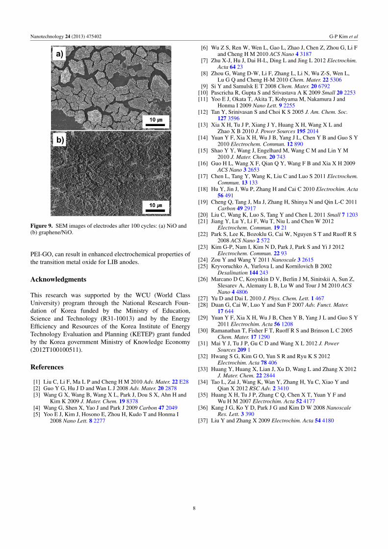
In order to further elucidate the effect of graphene asa provider of an electrical conductive network, impedancespectra were investigated for the pure NiO and graphene/NiOelectrodes during charge–discharge (second and 50th cycles),and the results are shown in figure 8. Apparently, the diameterof the semicircle for the graphene/NiO electrode is somewhatsmaller than that of the pure NiO film at the second cycle,indicating the smaller surface resistance and charge transferresistance [23, 32]. Thereafter, the impedance test at the endof 50 cycles indicated that NiO without graphene showsan increased charge transfer resistance (figure 8(a)). It ispossible that lithium-ion conduction inside the SEI layersand charge transfer at the electrode/electrolyte interface ishindered by the increase in internal defects and isolatedactive regions due to the volume change and subsequentmicrostructural failure during continued cycling [32, 35–37].In contrast, the semicircle, corresponding to the graphene/NiOfilm, shows extremely low charge transfer resistance after50 cycles (figure 8(b)). This behavior indicates that theNiO nanoparticles deposited on the graphene surface arefavorable for the formation of thicker SEI film [37]. Thegraphene/NiO structure appears to reach a stabilized state,which is consistent with the observed extra capacity of thegraphene/NiO electrode for up to 45 cycles (figure 6(c)).In addition, to confirm the structural integrity of theas-synthesized films, the evolution of the morphology andstructure of NiO and graphene/NiO were investigated after50 cycles, as shown in figure 9. The SEM image of theNiO film clearly shows that the deposited NiO suffers fromsevere cracking and subsequently deteriorates, with the filmbeing peeled off from the substrate (figure 9(a)). In contrast,the graphene/NiO retains its structural integrity with onlya slight deformation (figure 9(b)). The above results are
Figure 8. Impedance comparison curves: (a) NiO films and(b) graphene/NiO film.
consistent with the development of a synergistic effect asthe result of the NiO deposited on graphene, which leadsto an improved electrochemical performance. The highlyconductive graphene and interconnected NiO nanoparticlesfacilitate continuous conductive pathways for electrons andprovide a sufficient electrolyte contact area, resulting inthe formation of a stable SEI layer. Moreover, the uniquestructure of the electrodeposited graphene/NiO film caneffectively maintain its structural integrity by accommodatingthe pulverization of active materials during the cyclingprocess.
4. Conclusions
In summary, based on the finding that chemically PEI-GOcan be co-electrodeposited with positively charged metalprecursors under cathodic conditions, the one-step synthesisof interconnected NiO nanoparticles that are uniformlyelectrodeposited onto a graphene surface is successfullydemonstrated. The resultant thin film can be directly usedfor a LIB anode material. The reversible capacity andelectronic conductivity of the graphene/NiO are significantlyimproved. These enhancements result from the synergisticeffect of the graphene, which can assist electron transportand participate in the lithium storage process. We concludethat co-electrodeposition, when used in conjunction with
7
Nanotechnology 24 (2013) 475402 G-P Kim et al
Figure 9. SEM images of electrodes after 100 cycles: (a) NiO and(b) graphene/NiO.
PEI-GO, can result in enhanced electrochemical properties ofthe transition metal oxide for LIB anodes.
Acknowledgments
This research was supported by the WCU (World ClassUniversity) program through the National Research Foun-dation of Korea funded by the Ministry of Education,Science and Technology (R31-10013) and by the EnergyEfficiency and Resources of the Korea Institute of EnergyTechnology Evaluation and Planning (KETEP) grant fundedby the Korea government Ministry of Knowledge Economy(2012T100100511).
References
[1] Liu C, Li F, Ma L P and Cheng H M 2010 Adv. Mater. 22 E28[2] Guo Y G, Hu J D and Wan L J 2008 Adv. Mater. 20 2878[3] Wang G X, Wang B, Wang X L, Park J, Dou S X, Ahn H and
Kim K 2009 J. Mater. Chem. 19 8378[4] Wang G, Shen X, Yao J and Park J 2009 Carbon 47 2049[5] Yoo E J, Kim J, Hosono E, Zhou H, Kudo T and Honma I
2008 Nano Lett. 8 2277
[6] Wu Z S, Ren W, Wen L, Gao L, Zhao J, Chen Z, Zhou G, Li Fand Cheng H M 2010 ACS Nano 4 3187
[7] Zhu X-J, Hu J, Dai H-L, Ding L and Jing L 2012 Electrochim.Acta 64 23
[8] Zhou G, Wang D-W, Li F, Zhang L, Li N, Wu Z-S, Wen L,Lu G Q and Cheng H-M 2010 Chem. Mater. 22 5306
[9] Si Y and Samulsk E T 2008 Chem. Mater. 20 6792[10] Pascricha R, Gupta S and Srivastava A K 2009 Small 20 2253[11] Yoo E J, Okata T, Akita T, Kohyama M, Nakamura J and
Honma I 2009 Nano Lett. 9 2255[12] Tan Y, Srinivasan S and Choi K S 2005 J. Am. Chem. Soc.
127 3596[13] Xia X H, Tu J P, Xiang J Y, Huang X H, Wang X L and
Zhao X B 2010 J. Power Sources 195 2014[14] Yuan Y F, Xia X H, Wu J B, Yang J L, Chen Y B and Guo S Y
2010 Electrochem. Commun. 12 890[15] Shao Y Y, Wang J, Engelhard M, Wang C M and Lin Y M
2010 J. Mater. Chem. 20 743[16] Guo H L, Wang X F, Qian Q Y, Wang F B and Xia X H 2009
ACS Nano 3 2653[17] Chen L, Tang Y, Wang K, Liu C and Luo S 2011 Electrochem.
Commun. 13 133[18] Hu Y, Jin J, Wu P, Zhang H and Cai C 2010 Electrochim. Acta
56 491[19] Cheng Q, Tang J, Ma J, Zhang H, Shinya N and Qin L-C 2011
Carbon 49 2917[20] Liu C, Wang K, Luo S, Tang Y and Chen L 2011 Small 7 1203[21] Jiang Y, Lu Y, Li F, Wu T, Niu L and Chen W 2012
Electrochem. Commun. 19 21[22] Park S, Lee K, Bozoklu G, Cai W, Nguyen S T and Ruoff R S
2008 ACS Nano 2 572[23] Kim G-P, Nam I, Kim N D, Park J, Park S and Yi J 2012
Electrochem. Commun. 22 93[24] Zou Y and Wang Y 2011 Nanoscale 3 2615[25] Kryvoruchko A, Yurlova L and Kornilovich B 2002
Desalination 144 243[26] Marcano D C, Kosynkin D V, Berlin J M, Sinitskii A, Sun Z,
Slesarev A, Alemany L B, Lu W and Tour J M 2010 ACSNano 4 4806
[27] Yu D and Dai L 2010 J. Phys. Chem. Lett. 1 467[28] Duan G, Cai W, Luo Y and Sun F 2007 Adv. Funct. Mater.
17 644[29] Yuan Y F, Xia X H, Wu J B, Chen Y B, Yang J L and Guo S Y
2011 Electrochim. Acta 56 1208[30] Ramanathan T, Fisher F T, Ruoff R S and Brinson L C 2005
Chem. Mater. 17 1290[31] Mai Y J, Tu J P, Gu C D and Wang X L 2012 J. Power
Sources 209 1[32] Hwang S G, Kim G O, Yun S R and Ryu K S 2012
Electrochim. Acta 78 406[33] Huang Y, Huang X, Lian J, Xu D, Wang L and Zhang X 2012
J. Mater. Chem. 22 2844[34] Tao L, Zai J, Wang K, Wan Y, Zhang H, Yu C, Xiao Y and
Qian X 2012 RSC Adv. 2 3410[35] Huang X H, Tu J P, Zhang C Q, Chen X T, Yuan Y F and
Wu H M 2007 Electrochim. Acta 52 4177[36] Kang J G, Ko Y D, Park J G and Kim D W 2008 Nanoscale
Res. Lett. 3 390[37] Liu Y and Zhang X 2009 Electrochim. Acta 54 4180
8